EP3298627B1 - Packaging label and method for labelling a package - Google Patents
Packaging label and method for labelling a package Download PDFInfo
- Publication number
- EP3298627B1 EP3298627B1 EP16726047.0A EP16726047A EP3298627B1 EP 3298627 B1 EP3298627 B1 EP 3298627B1 EP 16726047 A EP16726047 A EP 16726047A EP 3298627 B1 EP3298627 B1 EP 3298627B1
- Authority
- EP
- European Patent Office
- Prior art keywords
- display
- control module
- substrate
- layer
- packaging label
- Prior art date
- Legal status (The legal status is an assumption and is not a legal conclusion. Google has not performed a legal analysis and makes no representation as to the accuracy of the status listed.)
- Active
Links
Images
Classifications
-
- G—PHYSICS
- G09—EDUCATION; CRYPTOGRAPHY; DISPLAY; ADVERTISING; SEALS
- G09F—DISPLAYING; ADVERTISING; SIGNS; LABELS OR NAME-PLATES; SEALS
- G09F3/00—Labels, tag tickets, or similar identification or indication means; Seals; Postage or like stamps
- G09F3/08—Fastening or securing by means not forming part of the material of the label itself
- G09F3/18—Casings, frames or enclosures for labels
- G09F3/20—Casings, frames or enclosures for labels for adjustable, removable, or interchangeable labels
- G09F3/208—Electronic labels, Labels integrating electronic displays
-
- H—ELECTRICITY
- H10—SEMICONDUCTOR DEVICES; ELECTRIC SOLID-STATE DEVICES NOT OTHERWISE PROVIDED FOR
- H10F—INORGANIC SEMICONDUCTOR DEVICES SENSITIVE TO INFRARED RADIATION, LIGHT, ELECTROMAGNETIC RADIATION OF SHORTER WAVELENGTH OR CORPUSCULAR RADIATION
- H10F77/00—Constructional details of devices covered by this subclass
- H10F77/10—Semiconductor bodies
- H10F77/14—Shape of semiconductor bodies; Shapes, relative sizes or dispositions of semiconductor regions within semiconductor bodies
- H10F77/143—Shape of semiconductor bodies; Shapes, relative sizes or dispositions of semiconductor regions within semiconductor bodies comprising quantum structures
- H10F77/1433—Quantum dots
-
- H—ELECTRICITY
- H10—SEMICONDUCTOR DEVICES; ELECTRIC SOLID-STATE DEVICES NOT OTHERWISE PROVIDED FOR
- H10K—ORGANIC ELECTRIC SOLID-STATE DEVICES
- H10K30/00—Organic devices sensitive to infrared radiation, light, electromagnetic radiation of shorter wavelength or corpuscular radiation
- H10K30/30—Organic devices sensitive to infrared radiation, light, electromagnetic radiation of shorter wavelength or corpuscular radiation comprising bulk heterojunctions, e.g. interpenetrating networks of donor and acceptor material domains
-
- H—ELECTRICITY
- H10—SEMICONDUCTOR DEVICES; ELECTRIC SOLID-STATE DEVICES NOT OTHERWISE PROVIDED FOR
- H10K—ORGANIC ELECTRIC SOLID-STATE DEVICES
- H10K59/00—Integrated devices, or assemblies of multiple devices, comprising at least one organic light-emitting element covered by group H10K50/00
- H10K59/10—OLED displays
- H10K59/221—Static displays, e.g. displaying permanent logos
-
- H—ELECTRICITY
- H10—SEMICONDUCTOR DEVICES; ELECTRIC SOLID-STATE DEVICES NOT OTHERWISE PROVIDED FOR
- H10K—ORGANIC ELECTRIC SOLID-STATE DEVICES
- H10K59/00—Integrated devices, or assemblies of multiple devices, comprising at least one organic light-emitting element covered by group H10K50/00
- H10K59/60—OLEDs integrated with inorganic light-sensitive elements, e.g. with inorganic solar cells or inorganic photodiodes
-
- G—PHYSICS
- G09—EDUCATION; CRYPTOGRAPHY; DISPLAY; ADVERTISING; SEALS
- G09F—DISPLAYING; ADVERTISING; SIGNS; LABELS OR NAME-PLATES; SEALS
- G09F3/00—Labels, tag tickets, or similar identification or indication means; Seals; Postage or like stamps
- G09F3/02—Forms or constructions
- G09F2003/0272—Labels for containers
-
- G—PHYSICS
- G09—EDUCATION; CRYPTOGRAPHY; DISPLAY; ADVERTISING; SEALS
- G09F—DISPLAYING; ADVERTISING; SIGNS; LABELS OR NAME-PLATES; SEALS
- G09F9/00—Indicating arrangements for variable information in which the information is built-up on a support by selection or combination of individual elements
- G09F9/30—Indicating arrangements for variable information in which the information is built-up on a support by selection or combination of individual elements in which the desired character or characters are formed by combining individual elements
-
- H—ELECTRICITY
- H10—SEMICONDUCTOR DEVICES; ELECTRIC SOLID-STATE DEVICES NOT OTHERWISE PROVIDED FOR
- H10F—INORGANIC SEMICONDUCTOR DEVICES SENSITIVE TO INFRARED RADIATION, LIGHT, ELECTROMAGNETIC RADIATION OF SHORTER WAVELENGTH OR CORPUSCULAR RADIATION
- H10F77/00—Constructional details of devices covered by this subclass
- H10F77/40—Optical elements or arrangements
- H10F77/42—Optical elements or arrangements directly associated or integrated with photovoltaic cells, e.g. light-reflecting means or light-concentrating means
-
- H—ELECTRICITY
- H10—SEMICONDUCTOR DEVICES; ELECTRIC SOLID-STATE DEVICES NOT OTHERWISE PROVIDED FOR
- H10K—ORGANIC ELECTRIC SOLID-STATE DEVICES
- H10K39/00—Integrated devices, or assemblies of multiple devices, comprising at least one organic radiation-sensitive element covered by group H10K30/00
- H10K39/10—Organic photovoltaic [PV] modules; Arrays of single organic PV cells
Definitions
- the present invention relates to a packaging label and to a method for labelling a package.
- labels with fixed graphics are known, i.e. bearing a predetermined message, which may be adhesive or printed directly onto the packaging, for example a plastic or glass bottle.
- the object of the invention is therefore to propose a dynamic label able to progressively change the contents displayed, which may be directly printed and/or integrated onto the packaging and which is compatible with current packaging production processes, by adding to the packaging itself a negligible cost in order to be economically sustainable.
- a further object of the invention is that of proposing an easily recyclable label.
- a label according to the present invention is fully recyclable, can be printed with high performance printing processes either on plastic or on paper or directly on plastic packaging, for example PET, and can be used with the current packaging industry standards.
- the label according to the present invention also integrates a source of independent energy.
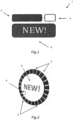
- Figure 1 shows a schematic front view of a label 1 not included in the scope of the present invention.
- label 1 comprises at least a photovoltaic source 2 adapted to supply a control module 4 and a display 6 bearing a message.
- the photovoltaic source 2 is a photovoltaic module known in itself, which preferably uses a bulk heterojunction organic technology. Alternatively, the photovoltaic source is not organic, being, for example, a photovoltaic source based on quantum dots or hybrid perovskite.
- the photovoltaic module 2 can be printed, in a known way, on a plastic substrate, for example, polyethylene terephthalate (PET) having a thickness preferably comprised in the interval 1 ⁇ m - 100 ⁇ m.
- PET polyethylene terephthalate
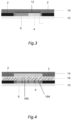
- Figure 2 shows a front view of an embodiment of the label 1, i.e. not included in the scope of present invention, in which there are a plurality of photovoltaic modules 2 arranged along a circumference, the display 6 corresponding to the area containing the message and the control module 4 being next to the display 6 (according to an embodiment of the present invention, the control module 4 is positioned below the display 6 as described in detail below).
- Such a procedure starts with a first step 100 of providing a substrate 10, preferably of the type described above.
- a substrate 10 may be transparent or opaque.
- the label is printed directly on the packaging (e.g. a plastic bottle or paper box), in which case the substrate is the surface of the packaging itself.
- the substrate could be made of (or including) other materials, e.g. metal foils, rubber, self-adhesive substrate, tattoo paper.
- Figure 3 shows a sectional view of the label 1, i.e. not included in the scope of present invention, in which the substrate 10 is present preferably a plastic sheet or bottle, onto which, in step 102 the photovoltaic module is printed.
- the control module 4 preferably comprising at least a low power supply thin film transistor, and the display 6 are printed, respectively, the latter preferably provided in the form of a layer of electrically addressable material, e.g. and electrochromic material.
- the layer could be made of any other electrically addressable material, e.g. electroluminescent material.
- a fundamental limit connected with organic electronic printing (steps 102 - 106 described above) on thin (10-200 ⁇ m) and ultrathin (less than 10 ⁇ m) plastic supports is connected with the maximum temperature of the printing process.
- thermal heating processes are required, which are not compatible with the thin layer of plastic substrate used in the packaging, since such a layer would be heat sensitive.
- the optimisation of the organic electronic printing process is closely connected with the annealing processes, which typically require temperatures of over 100°C, necessary for optimising the performance of the printed devices, for example, improving the mobility of charge carriers, de-absorbing contaminants and obtaining the desired morphology of the support layer.
- ink is used which is in itself known, to which, before performing the printing itself, dopants are added, preferably precursors of benzimidazole and benzimidazoline or caesium or lithium salts.
- optimised electronics are obtained, printed directly at room temperature or however at low temperatures compatible with the substrate 10 (preferably lower than 70°C), in which only the evaporation of the ink solvent is required.
- the control module 4 is provided to send control signals to the display 6 so that predetermined messages are shown on the display 6.
- control module 4 and the display 6 are in electrical contact with the photovoltaic module 2 for allowing its supply by the latter.
- an electrical interconnecting layer 12 is provided, through the holes (see Figure 4 ) preferably of ion-gel or solid electrolyte type, which allows the control module 4 to perform a low voltage control of the display 6, i.e. allowing the control module 4 to send control signals to the display 6.
- control module 4 is provided through at least one thin film transistor comprising semiconductor metal oxides such as, for example, ZnO, IZO, IGZO.
- a barrier layer 14 is deposited, preferably oxide/polymer multilayer, for example silica and alumina for the inorganic layer and EVA, ETFE, PET or PEN for the organic layer, so as to protect the underlying layers from oxygen and water vapour.
- oxide/polymer multilayer for example silica and alumina for the inorganic layer and EVA, ETFE, PET or PEN for the organic layer, so as to protect the underlying layers from oxygen and water vapour.
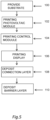
- FIG. 4 shows a preferred embodiment of the invention wherein similar layers are indicated with the same reference numbers.
- the display 6 is placed between two photovoltaic modules 2 above the substrate 10.
- an insulating layer 16 is first deposited, having a predetermined pattern, i.e. a plurality of holes 16a placed in correspondence of the display 6 and subsequently the control module 4 is deposited which, through the holes 16a, comes into contact with the display 6 below.
- the barrier layer 14 is deposited above the control module 4 deposited.
- the label 1 according to the present invention is recyclable because all the electronic components are made with plastic electronic materials or easily separable from plastic (metallisations of silver or other metals).
- the active label 1 is also recyclable because the materials of which each of its components are comprised, i.e. the photovoltaic module 2, the control module 4 and the display 6 are characterised by a low melting temperature (comprised between 200 and 400 °C). In this way, any traces of non-plastic materials (metals, metal oxides, etc.) present in the label 1 can be removed by filtering, in a known way, through techniques for the purification of recycled plastic.
Landscapes
- Physics & Mathematics (AREA)
- General Physics & Mathematics (AREA)
- Engineering & Computer Science (AREA)
- Theoretical Computer Science (AREA)
- Life Sciences & Earth Sciences (AREA)
- Chemical & Material Sciences (AREA)
- Inorganic Chemistry (AREA)
- Sustainable Development (AREA)
- Electromagnetism (AREA)
- Details Of Rigid Or Semi-Rigid Containers (AREA)
- Packages (AREA)
Description
- The present invention relates to a packaging label and to a method for labelling a package.
- In the packaging industry labels with fixed graphics are known, i.e. bearing a predetermined message, which may be adhesive or printed directly onto the packaging, for example a plastic or glass bottle.
- However, such labels have the disadvantage of being able to produce only one message (e.g. product name, list of ingredients, promotional message), therefore for many commercial products, it is necessary to use a plurality of different labels, each dedicated to specific contents.
- In the field of electronics on plastic, dynamic labels are also known, provided with a display for displaying a plurality of different messages, such as, for example, a promotional message, the expiry date and/or the ingredients of the packaged product. However, such labels are not fully comprised of materials compatible with recycling (including the display) and the production process is not compatible with high performance printing or with direct printing on the packaging container. Furthermore, such labels must be self-supplied and not even the supply unit satisfies the above indicated requirements. Documents
US 2015/108508 A1 ,US 2012/326131 A1 ,US 2011/317121 A1 andUS 2011/096388 A1 disclose examples of packaging labels according to prior art. - Therefore, there is a need to find innovative solutions to the problem of "dynamically" labelling packaged products, mainly for marketing and advertising purposes.
- The object of the invention is therefore to propose a dynamic label able to progressively change the contents displayed, which may be directly printed and/or integrated onto the packaging and which is compatible with current packaging production processes, by adding to the packaging itself a negligible cost in order to be economically sustainable.
- A further object of the invention is that of proposing an easily recyclable label.
- These and other objects are reached with a label whose characteristics are defined in
claim 1. - Particular embodiments form the subject matter of the dependent claims, whose contents are to be considered an integral part of the present description.
- Further characteristics and advantages of the invention will appear from the following detailed description, given by way of non-limitative example, with reference to the appended drawings, in which:
-
Figure 1 is a schematic front view of a label according to an embodiment not included in the scope of the present invention; -
Figure 2 illustrates a front view of an embodiment of the label ofFigure 1 ; -
Figure 3 shows a sectional view of the label ofFigure 1 ; -
Figure 4 shows the label according to a preferred embodiment of the present invention; and -
Figure 5 shows a block diagram of the operations of the method for obtaining a label according to the present invention. - In summary, a label according to the present invention is fully recyclable, can be printed with high performance printing processes either on plastic or on paper or directly on plastic packaging, for example PET, and can be used with the current packaging industry standards. The label according to the present invention also integrates a source of independent energy.
-
Figure 1 shows a schematic front view of alabel 1 not included in the scope of the present invention.Such label 1 comprises at least aphotovoltaic source 2 adapted to supply acontrol module 4 and adisplay 6 bearing a message. - The
photovoltaic source 2 is a photovoltaic module known in itself, which preferably uses a bulk heterojunction organic technology. Alternatively, the photovoltaic source is not organic, being, for example, a photovoltaic source based on quantum dots or hybrid perovskite. Thephotovoltaic module 2 can be printed, in a known way, on a plastic substrate, for example, polyethylene terephthalate (PET) having a thickness preferably comprised in the interval 1µm - 100 µm. -
Figure 2 shows a front view of an embodiment of thelabel 1, i.e. not included in the scope of present invention, in which there are a plurality ofphotovoltaic modules 2 arranged along a circumference, thedisplay 6 corresponding to the area containing the message and thecontrol module 4 being next to the display 6 (according to an embodiment of the present invention, thecontrol module 4 is positioned below thedisplay 6 as described in detail below). - Below, with reference to
figure 4 , the process will be described for obtaining a label according to the present invention, the block diagram of which is shown infigure 5 . Such a procedure starts with afirst step 100 of providing asubstrate 10, preferably of the type described above.Such substrate 10 may be transparent or opaque. In an embodiment of the present invention, the label is printed directly on the packaging (e.g. a plastic bottle or paper box), in which case the substrate is the surface of the packaging itself. Alternatively the substrate could be made of (or including) other materials, e.g. metal foils, rubber, self-adhesive substrate, tattoo paper. -
Figure 3 shows a sectional view of thelabel 1, i.e. not included in the scope of present invention, in which thesubstrate 10 is present preferably a plastic sheet or bottle, onto which, instep 102 the photovoltaic module is printed. Between thephotovoltaic modules 2 insteps control module 4, preferably comprising at least a low power supply thin film transistor, and thedisplay 6 are printed, respectively, the latter preferably provided in the form of a layer of electrically addressable material, e.g. and electrochromic material. Alternatively the layer could be made of any other electrically addressable material, e.g. electroluminescent material. - A fundamental limit connected with organic electronic printing (steps 102 - 106 described above) on thin (10-200 µm) and ultrathin (less than 10 µm) plastic supports is connected with the maximum temperature of the printing process. Typically, to perform such printing, thermal heating processes are required, which are not compatible with the thin layer of plastic substrate used in the packaging, since such a layer would be heat sensitive. The optimisation of the organic electronic printing process is closely connected with the annealing processes, which typically require temperatures of over 100°C, necessary for optimising the performance of the printed devices, for example, improving the mobility of charge carriers, de-absorbing contaminants and obtaining the desired morphology of the support layer.
- In the printing operations 102-106 described above, ink is used which is in itself known, to which, before performing the printing itself, dopants are added, preferably precursors of benzimidazole and benzimidazoline or caesium or lithium salts.
- Thanks to the use of these particular chemical dopants, optimised electronics are obtained, printed directly at room temperature or however at low temperatures compatible with the substrate 10 (preferably lower than 70°C), in which only the evaporation of the ink solvent is required.
- The
control module 4 is provided to send control signals to thedisplay 6 so that predetermined messages are shown on thedisplay 6. - The
control module 4 and thedisplay 6 are in electrical contact with thephotovoltaic module 2 for allowing its supply by the latter. - Above the
control module 4 and thedisplay 6, instep 108, anelectrical interconnecting layer 12 is provided, through the holes (seeFigure 4 ) preferably of ion-gel or solid electrolyte type, which allows thecontrol module 4 to perform a low voltage control of thedisplay 6, i.e. allowing thecontrol module 4 to send control signals to thedisplay 6. - Alternatively, the
control module 4 is provided through at least one thin film transistor comprising semiconductor metal oxides such as, for example, ZnO, IZO, IGZO. - Finally, in
step 110, on top of all the underlying layers, abarrier layer 14 is deposited, preferably oxide/polymer multilayer, for example silica and alumina for the inorganic layer and EVA, ETFE, PET or PEN for the organic layer, so as to protect the underlying layers from oxygen and water vapour. -
Figure 4 shows a preferred embodiment of the invention wherein similar layers are indicated with the same reference numbers. As represented on this Figure, only thedisplay 6 is placed between twophotovoltaic modules 2 above thesubstrate 10. Above thephotovoltaic modules 2 and thedisplay 6 aninsulating layer 16 is first deposited, having a predetermined pattern, i.e. a plurality of holes 16a placed in correspondence of thedisplay 6 and subsequently thecontrol module 4 is deposited which, through the holes 16a, comes into contact with thedisplay 6 below. Finally, above thecontrol module 4 thebarrier layer 14 is deposited. - Therefore, in this embodiment, during use, there will be the
front display 6 and thecontrol module 4 behind it. - The
label 1 according to the present invention is recyclable because all the electronic components are made with plastic electronic materials or easily separable from plastic (metallisations of silver or other metals). - The
active label 1 is also recyclable because the materials of which each of its components are comprised, i.e. thephotovoltaic module 2, thecontrol module 4 and thedisplay 6 are characterised by a low melting temperature (comprised between 200 and 400 °C). In this way, any traces of non-plastic materials (metals, metal oxides, etc.) present in thelabel 1 can be removed by filtering, in a known way, through techniques for the purification of recycled plastic. - The scope of the present invention is defined by the appended claims.
Claims (13)
- Packaging label (1) comprising:- a flexible substrate (10);- a printed display (6) above the substrate (10), the display comprising an electrically addressable layer of ink;- a printed control module (4) above the substrate, in electrical contact with the display (6) and arranged to control the operating of such display (6), the control module including a layer comprising ink mixed with dopants;- at least a printed photovoltaic module (2) above the substrate (10) and next to the display (6) and arranged to supply the display (6) and the control module (4), the photovoltaic module including a layer comprising ink mixed with dopants, characterised by further comprising an insulating layer (16) placed above the display (6) and on which the control module (4) is placed, said insulating layer (16) having a plurality of holes (16a) placed in correspondence of the display (6) and arranged to allow the electric contact between said display (6) and the control module (4).
- Packaging label according to claim 1 wherein the substrate is made of one or more material selected in the following: plastic, paper, metal foils, rubber, self-adhesive substrate, tattoo paper.
- Packaging label according to any preceding claim wherein the display includes a layer of electrochromic ink.
- Packaging label according to any preceding claim wherein the substrate has a thickness between 1 and 100 µm.
- Packaging label according to any preceding claim, wherein the dopants include a precursor of benzimidazole or benzimidazoline or caesium or lithium salts.
- Packaging label according to any preceding claim, wherein the electric contact between the control module (4) and the display (6) comprises an inter-connecting layer (12) of ion-gel or solid electrolyte, the inter-connecting layer having also the function of Ion reservoir for the electrochromic display and/or gate medium for the transistors in the control unit.
- Packaging label according to any preceding claim, wherein the control module (4) comprises a low-voltage organic thin layer transistor.
- Packaging label Label according to any of the claims 1 to 6, wherein the control module (4) comprises at least a thin film transistor comprising semiconductor metal oxides.
- Packaging label according to any preceding claim, further comprising a barrier layer (14) placed above the control module (4).
- Method of obtaining a packaging label (1) for packaging comprising the steps of:- printing (102) on a substrate (10) at least one photovoltaic module (2);- printing (104, 106), next to the photovoltaic module (2), a display (6);- depositing an insulating layer (16) above the display (6), the insulating layer (16) having a plurality of holes (16a) placed in correspondence of the display (6);- printing a control module (4) above the insulating layer (16), arranging an electrical interconnection through the holes adapted to allow the display (6) to electrically contact the control module (4) and to allow the control module (4) to control the display (6); wherein the printing steps (102, 104, 106) of the photovoltaic module (2), the control module (4) and the display (6) comprise the step of mixing a printing ink with dopants.
- Method according to claim 10 further comprising the step of depositing (110) a barrier layer (14), arranged to protect the underlying layers.
- Method of labelling a package including the steps of claim 10, wherein the substrate is the surface of the package.
- A packaging including a packaging label according to any of claims 1-9.
Applications Claiming Priority (2)
| Application Number | Priority Date | Filing Date | Title |
|---|---|---|---|
| ITUB20150644 | 2015-05-20 | ||
| PCT/EP2016/061324 WO2016184982A1 (en) | 2015-05-20 | 2016-05-19 | Packaging label and method for labelling a package |
Publications (3)
| Publication Number | Publication Date |
|---|---|
| EP3298627A1 EP3298627A1 (en) | 2018-03-28 |
| EP3298627B1 true EP3298627B1 (en) | 2024-11-06 |
| EP3298627C0 EP3298627C0 (en) | 2024-11-06 |
Family
ID=53900975
Family Applications (1)
| Application Number | Title | Priority Date | Filing Date |
|---|---|---|---|
| EP16726047.0A Active EP3298627B1 (en) | 2015-05-20 | 2016-05-19 | Packaging label and method for labelling a package |
Country Status (6)
| Country | Link |
|---|---|
| US (1) | US20180240376A1 (en) |
| EP (1) | EP3298627B1 (en) |
| KR (1) | KR20180034328A (en) |
| CN (1) | CN107924935B (en) |
| CA (1) | CA2985701A1 (en) |
| WO (1) | WO2016184982A1 (en) |
Families Citing this family (5)
| Publication number | Priority date | Publication date | Assignee | Title |
|---|---|---|---|---|
| US10672960B2 (en) | 2017-10-19 | 2020-06-02 | Lumileds Llc | Light emitting device package with a coating layer |
| WO2020076876A1 (en) | 2018-10-09 | 2020-04-16 | Reelables, Inc. | Low-power electronic tape for tracking items |
| US12322270B2 (en) | 2018-10-09 | 2025-06-03 | Reelables, Inc. | Method of fabrication of low-power electronic tape for tracking items |
| IT202100025613A1 (en) * | 2021-10-07 | 2023-04-07 | Omet Srl | TAMPER-RESISTANT LABEL FOR A PRODUCT PACKAGING AND RELATED METHOD FOR CREATING THE TAMPER-RESISTANT LABEL AND PRODUCT PACKAGING |
| CN115202125A (en) * | 2022-07-08 | 2022-10-18 | 惠科股份有限公司 | Display panel and display module |
Citations (2)
| Publication number | Priority date | Publication date | Assignee | Title |
|---|---|---|---|---|
| US20110096388A1 (en) * | 2008-07-03 | 2011-04-28 | Ajjer Llc | Flexible and printable electrooptic devices |
| US20120168910A1 (en) * | 2011-01-05 | 2012-07-05 | Jackrel David B | Multi-nary group ib and via based semiconductor |
Family Cites Families (15)
| Publication number | Priority date | Publication date | Assignee | Title |
|---|---|---|---|---|
| EP0428383A1 (en) * | 1989-11-13 | 1991-05-22 | Shikoku Chemicals Corporation | Process for surface treatment of copper and copper alloy |
| TW495812B (en) * | 2000-03-06 | 2002-07-21 | Semiconductor Energy Lab | Thin film forming device, method of forming a thin film, and self-light-emitting device |
| WO2003057500A1 (en) * | 2002-01-10 | 2003-07-17 | Bundesdruckerei Gmbh | Valuable document or security document comprising a switch |
| US6886864B2 (en) * | 2002-10-09 | 2005-05-03 | Hewlett-Packard Development Company, L.P. | Flexible sheet having at least one region of electroluminescence |
| KR20070086572A (en) * | 2004-11-23 | 2007-08-27 | 오렐 퓌슬리 지혀하이츠드럭 에이지 | Security document with light source and light processing device |
| US20070114366A1 (en) * | 2005-11-21 | 2007-05-24 | General Electric Company | Optical article having a multi-component structure as an anti-theft feature and a system and method for inhibiting theft of same |
| EP1936603A1 (en) * | 2006-12-19 | 2008-06-25 | European Central Bank | Security document comprising an electrochromic element |
| US9892663B2 (en) * | 2008-07-03 | 2018-02-13 | Chromera, Inc. | Intelligent label device and method |
| TW201034269A (en) * | 2009-03-13 | 2010-09-16 | Nat Univ Tsing Hua | Organic thin film transistor which contains azole complex to dielectric insulating layer |
| CN101840996A (en) * | 2009-03-20 | 2010-09-22 | 德晶电子(江苏)有限公司 | Printed semiconductor transistor and forming method thereof |
| US8253536B2 (en) * | 2009-04-22 | 2012-08-28 | Simon Fraser University | Security document with electroactive polymer power source and nano-optical display |
| KR20110070167A (en) * | 2009-12-18 | 2011-06-24 | 엘지디스플레이 주식회사 | Organic light emitting device |
| TWI406036B (en) * | 2010-06-28 | 2013-08-21 | Au Optronics Corp | Solar cell integrated liquid crystal display device and solar cell integrated flat display device |
| KR20130006936A (en) * | 2011-06-27 | 2013-01-18 | 삼성디스플레이 주식회사 | Organic light emitting display |
| US9356179B2 (en) * | 2012-06-22 | 2016-05-31 | Industrial Technology Research Institute | Display panel integrated with photoelectric device |
-
2016
- 2016-05-19 CA CA2985701A patent/CA2985701A1/en not_active Abandoned
- 2016-05-19 EP EP16726047.0A patent/EP3298627B1/en active Active
- 2016-05-19 CN CN201680028372.2A patent/CN107924935B/en active Active
- 2016-05-19 KR KR1020177036563A patent/KR20180034328A/en not_active Ceased
- 2016-05-19 WO PCT/EP2016/061324 patent/WO2016184982A1/en not_active Ceased
- 2016-05-19 US US15/574,033 patent/US20180240376A1/en not_active Abandoned
Patent Citations (2)
| Publication number | Priority date | Publication date | Assignee | Title |
|---|---|---|---|---|
| US20110096388A1 (en) * | 2008-07-03 | 2011-04-28 | Ajjer Llc | Flexible and printable electrooptic devices |
| US20120168910A1 (en) * | 2011-01-05 | 2012-07-05 | Jackrel David B | Multi-nary group ib and via based semiconductor |
Non-Patent Citations (2)
| Title |
|---|
| ANONYMOUS: "Transistor - Wikipedia", 18 December 2003 (2003-12-18), XP093022970, Retrieved from the Internet <URL:https://en.wikipedia.org/wiki/Transistor> [retrieved on 20230210] * |
| BERND TIEKE ED - MILLER REINHARD ET AL: "Coordinative supramolecular assembly of electrochromic thin films", CURRENT OPINION IN COLLOID & INTERFACE SCIENCE, LONDON, GB, vol. 16, no. 6, 20 June 2011 (2011-06-20), pages 499 - 507, XP028114218, ISSN: 1359-0294, [retrieved on 20110729], DOI: 10.1016/J.COCIS.2011.07.002 * |
Also Published As
| Publication number | Publication date |
|---|---|
| CA2985701A1 (en) | 2016-11-24 |
| WO2016184982A1 (en) | 2016-11-24 |
| CN107924935B (en) | 2021-10-29 |
| EP3298627A1 (en) | 2018-03-28 |
| CN107924935A (en) | 2018-04-17 |
| EP3298627C0 (en) | 2024-11-06 |
| US20180240376A1 (en) | 2018-08-23 |
| KR20180034328A (en) | 2018-04-04 |
Similar Documents
| Publication | Publication Date | Title |
|---|---|---|
| US20180240376A1 (en) | Packaging label and method for labelling a package | |
| JP6970160B2 (en) | Semiconductor device | |
| US11951726B2 (en) | Method of manufacturing a flexible display substrate and process film for manufacturing a flexible display substrate | |
| Lee et al. | Skin‐like oxide thin‐film transistors for transparent displays | |
| KR101254277B1 (en) | Laminating system, IC sheet, scroll of IC sheet, and method for manufacturing IC chip | |
| CN100550328C (en) | Lamination system, IC wafer and roll, and method for manufacturing IC chips | |
| Lupo et al. | OE-A roadmap for organic and printed electronics | |
| US20090261062A1 (en) | Carrier substrate and method of manufacturing flexible display apparatus using the same | |
| Hast et al. | 18.1: Invited paper: Roll‐to‐roll manufacturing of printed OLEDs | |
| KR101726916B1 (en) | Cover window formed with printing layer for touch screen panel and method for forming printing layer on cover window for touch screen panel | |
| US20170069870A1 (en) | Display panel, method for packaging the same, and display device | |
| US20190386215A1 (en) | Stripping method of flexible oled display device | |
| US20050156244A1 (en) | Thin film apparatus, a manufacturing method of the thin film apparatus, an active matrix substrate, a manufacturing method of the active matrix substrate, and an electro-optical apparatus having the active matrix substrate | |
| JP5898949B2 (en) | Method for manufacturing flexible device | |
| US10355228B2 (en) | Method of manufacturing flexible substrate and flexible substrate | |
| US20180277573A1 (en) | Display device and method for producing display device | |
| JP2019207705A (en) | Information processor | |
| CN106585069A (en) | Flexible substrate, panel and method of manufacturing flexible substrate and panel by screen printer | |
| US20200410905A1 (en) | Packaging label and method for labelling a package | |
| Sircar et al. | An introduction to flexible electronics: Manufacturing techniques, types and future | |
| KR101191519B1 (en) | Paper-based electronic device and method for manufacturing the same | |
| Ning et al. | Inkjet printing satellite-free silver electrodes array in a-IGZO TFTs by regulating piezoelectric waveforms | |
| Zipperer | Printed Electronics for Flexible Applications | |
| JP2005535050A (en) | Chip card with integrated energy converter | |
| Okandan et al. | Flexible Glass for Microelectronics Integration |
Legal Events
| Date | Code | Title | Description |
|---|---|---|---|
| STAA | Information on the status of an ep patent application or granted ep patent |
Free format text: STATUS: THE INTERNATIONAL PUBLICATION HAS BEEN MADE |
|
| PUAI | Public reference made under article 153(3) epc to a published international application that has entered the european phase |
Free format text: ORIGINAL CODE: 0009012 |
|
| STAA | Information on the status of an ep patent application or granted ep patent |
Free format text: STATUS: REQUEST FOR EXAMINATION WAS MADE |
|
| 17P | Request for examination filed |
Effective date: 20171107 |
|
| AK | Designated contracting states |
Kind code of ref document: A1 Designated state(s): AL AT BE BG CH CY CZ DE DK EE ES FI FR GB GR HR HU IE IS IT LI LT LU LV MC MK MT NL NO PL PT RO RS SE SI SK SM TR |
|
| AX | Request for extension of the european patent |
Extension state: BA ME |
|
| DAV | Request for validation of the european patent (deleted) | ||
| DAX | Request for extension of the european patent (deleted) | ||
| STAA | Information on the status of an ep patent application or granted ep patent |
Free format text: STATUS: EXAMINATION IS IN PROGRESS |
|
| 17Q | First examination report despatched |
Effective date: 20210616 |
|
| REG | Reference to a national code |
Ref country code: DE Ref legal event code: R079 Free format text: PREVIOUS MAIN CLASS: H01L0027320000 Ipc: G09F0003200000 Ref document number: 602016090123 Country of ref document: DE |
|
| GRAP | Despatch of communication of intention to grant a patent |
Free format text: ORIGINAL CODE: EPIDOSNIGR1 |
|
| STAA | Information on the status of an ep patent application or granted ep patent |
Free format text: STATUS: GRANT OF PATENT IS INTENDED |
|
| RIC1 | Information provided on ipc code assigned before grant |
Ipc: G09F 3/02 20060101ALN20240507BHEP Ipc: H10K 59/60 20230101ALI20240507BHEP Ipc: H10K 59/10 20230101ALI20240507BHEP Ipc: G09F 9/30 20060101ALI20240507BHEP Ipc: G09F 3/20 20060101AFI20240507BHEP |
|
| RIC1 | Information provided on ipc code assigned before grant |
Ipc: G09F 3/02 20060101ALN20240515BHEP Ipc: H10K 59/60 20230101ALI20240515BHEP Ipc: H10K 59/10 20230101ALI20240515BHEP Ipc: G09F 9/30 20060101ALI20240515BHEP Ipc: G09F 3/20 20060101AFI20240515BHEP |
|
| RIC1 | Information provided on ipc code assigned before grant |
Ipc: G09F 3/02 20060101ALN20240521BHEP Ipc: H10K 59/60 20230101ALI20240521BHEP Ipc: H10K 59/10 20230101ALI20240521BHEP Ipc: G09F 9/30 20060101ALI20240521BHEP Ipc: G09F 3/20 20060101AFI20240521BHEP |
|
| INTG | Intention to grant announced |
Effective date: 20240607 |
|
| GRAS | Grant fee paid |
Free format text: ORIGINAL CODE: EPIDOSNIGR3 |
|
| GRAA | (expected) grant |
Free format text: ORIGINAL CODE: 0009210 |
|
| STAA | Information on the status of an ep patent application or granted ep patent |
Free format text: STATUS: THE PATENT HAS BEEN GRANTED |
|
| AK | Designated contracting states |
Kind code of ref document: B1 Designated state(s): AL AT BE BG CH CY CZ DE DK EE ES FI FR GB GR HR HU IE IS IT LI LT LU LV MC MK MT NL NO PL PT RO RS SE SI SK SM TR |
|
| REG | Reference to a national code |
Ref country code: GB Ref legal event code: FG4D |
|
| REG | Reference to a national code |
Ref country code: CH Ref legal event code: EP |
|
| REG | Reference to a national code |
Ref country code: DE Ref legal event code: R096 Ref document number: 602016090123 Country of ref document: DE |
|
| REG | Reference to a national code |
Ref country code: IE Ref legal event code: FG4D |
|
| U01 | Request for unitary effect filed |
Effective date: 20241114 |
|
| U07 | Unitary effect registered |
Designated state(s): AT BE BG DE DK EE FI FR IT LT LU LV MT NL PT RO SE SI Effective date: 20241120 |
|
| PG25 | Lapsed in a contracting state [announced via postgrant information from national office to epo] |
Ref country code: HR Free format text: LAPSE BECAUSE OF FAILURE TO SUBMIT A TRANSLATION OF THE DESCRIPTION OR TO PAY THE FEE WITHIN THE PRESCRIBED TIME-LIMIT Effective date: 20241106 Ref country code: IS Free format text: LAPSE BECAUSE OF FAILURE TO SUBMIT A TRANSLATION OF THE DESCRIPTION OR TO PAY THE FEE WITHIN THE PRESCRIBED TIME-LIMIT Effective date: 20250306 |
|
| PG25 | Lapsed in a contracting state [announced via postgrant information from national office to epo] |
Ref country code: ES Free format text: LAPSE BECAUSE OF FAILURE TO SUBMIT A TRANSLATION OF THE DESCRIPTION OR TO PAY THE FEE WITHIN THE PRESCRIBED TIME-LIMIT Effective date: 20241106 |
|
| PG25 | Lapsed in a contracting state [announced via postgrant information from national office to epo] |
Ref country code: NO Free format text: LAPSE BECAUSE OF FAILURE TO SUBMIT A TRANSLATION OF THE DESCRIPTION OR TO PAY THE FEE WITHIN THE PRESCRIBED TIME-LIMIT Effective date: 20250206 |
|
| PG25 | Lapsed in a contracting state [announced via postgrant information from national office to epo] |
Ref country code: GR Free format text: LAPSE BECAUSE OF FAILURE TO SUBMIT A TRANSLATION OF THE DESCRIPTION OR TO PAY THE FEE WITHIN THE PRESCRIBED TIME-LIMIT Effective date: 20250207 |
|
| PG25 | Lapsed in a contracting state [announced via postgrant information from national office to epo] |
Ref country code: PL Free format text: LAPSE BECAUSE OF FAILURE TO SUBMIT A TRANSLATION OF THE DESCRIPTION OR TO PAY THE FEE WITHIN THE PRESCRIBED TIME-LIMIT Effective date: 20241106 |
|
| PG25 | Lapsed in a contracting state [announced via postgrant information from national office to epo] |
Ref country code: RS Free format text: LAPSE BECAUSE OF FAILURE TO SUBMIT A TRANSLATION OF THE DESCRIPTION OR TO PAY THE FEE WITHIN THE PRESCRIBED TIME-LIMIT Effective date: 20250206 |
|
| U20 | Renewal fee for the european patent with unitary effect paid |
Year of fee payment: 10 Effective date: 20250527 |
|
| PG25 | Lapsed in a contracting state [announced via postgrant information from national office to epo] |
Ref country code: SM Free format text: LAPSE BECAUSE OF FAILURE TO SUBMIT A TRANSLATION OF THE DESCRIPTION OR TO PAY THE FEE WITHIN THE PRESCRIBED TIME-LIMIT Effective date: 20241106 |
|
| PGFP | Annual fee paid to national office [announced via postgrant information from national office to epo] |
Ref country code: GB Payment date: 20250523 Year of fee payment: 10 |
|
| PG25 | Lapsed in a contracting state [announced via postgrant information from national office to epo] |
Ref country code: SK Free format text: LAPSE BECAUSE OF FAILURE TO SUBMIT A TRANSLATION OF THE DESCRIPTION OR TO PAY THE FEE WITHIN THE PRESCRIBED TIME-LIMIT Effective date: 20241106 |
|
| PG25 | Lapsed in a contracting state [announced via postgrant information from national office to epo] |
Ref country code: CZ Free format text: LAPSE BECAUSE OF FAILURE TO SUBMIT A TRANSLATION OF THE DESCRIPTION OR TO PAY THE FEE WITHIN THE PRESCRIBED TIME-LIMIT Effective date: 20241106 |
|
| PLBE | No opposition filed within time limit |
Free format text: ORIGINAL CODE: 0009261 |
|
| STAA | Information on the status of an ep patent application or granted ep patent |
Free format text: STATUS: NO OPPOSITION FILED WITHIN TIME LIMIT |
|
| 26N | No opposition filed |
Effective date: 20250807 |
|
| REG | Reference to a national code |
Ref country code: CH Ref legal event code: H13 Free format text: ST27 STATUS EVENT CODE: U-0-0-H10-H13 (AS PROVIDED BY THE NATIONAL OFFICE) Effective date: 20251223 |
|
| PG25 | Lapsed in a contracting state [announced via postgrant information from national office to epo] |
Ref country code: CH Free format text: LAPSE BECAUSE OF NON-PAYMENT OF DUE FEES Effective date: 20250531 |
|
| PG25 | Lapsed in a contracting state [announced via postgrant information from national office to epo] |
Ref country code: MC Free format text: LAPSE BECAUSE OF FAILURE TO SUBMIT A TRANSLATION OF THE DESCRIPTION OR TO PAY THE FEE WITHIN THE PRESCRIBED TIME-LIMIT Effective date: 20241106 |
|
| PG25 | Lapsed in a contracting state [announced via postgrant information from national office to epo] |
Ref country code: IE Free format text: LAPSE BECAUSE OF NON-PAYMENT OF DUE FEES Effective date: 20250519 |