EP3297028A1 - Light emitting diode display device - Google Patents
Light emitting diode display device Download PDFInfo
- Publication number
- EP3297028A1 EP3297028A1 EP17191903.8A EP17191903A EP3297028A1 EP 3297028 A1 EP3297028 A1 EP 3297028A1 EP 17191903 A EP17191903 A EP 17191903A EP 3297028 A1 EP3297028 A1 EP 3297028A1
- Authority
- EP
- European Patent Office
- Prior art keywords
- slit
- semiconductor
- emitting diode
- light emitting
- electrode
- Prior art date
- Legal status (The legal status is an assumption and is not a legal conclusion. Google has not performed a legal analysis and makes no representation as to the accuracy of the status listed.)
- Granted
Links
Images







Classifications
-
- H—ELECTRICITY
- H10—SEMICONDUCTOR DEVICES; ELECTRIC SOLID-STATE DEVICES NOT OTHERWISE PROVIDED FOR
- H10K—ORGANIC ELECTRIC SOLID-STATE DEVICES
- H10K59/00—Integrated devices, or assemblies of multiple devices, comprising at least one organic light-emitting element covered by group H10K50/00
- H10K59/10—OLED displays
- H10K59/12—Active-matrix OLED [AMOLED] displays
- H10K59/126—Shielding, e.g. light-blocking means over the TFTs
-
- H—ELECTRICITY
- H10—SEMICONDUCTOR DEVICES; ELECTRIC SOLID-STATE DEVICES NOT OTHERWISE PROVIDED FOR
- H10K—ORGANIC ELECTRIC SOLID-STATE DEVICES
- H10K59/00—Integrated devices, or assemblies of multiple devices, comprising at least one organic light-emitting element covered by group H10K50/00
- H10K59/10—OLED displays
- H10K59/12—Active-matrix OLED [AMOLED] displays
- H10K59/131—Interconnections, e.g. wiring lines or terminals
-
- H—ELECTRICITY
- H10—SEMICONDUCTOR DEVICES; ELECTRIC SOLID-STATE DEVICES NOT OTHERWISE PROVIDED FOR
- H10D—INORGANIC ELECTRIC SEMICONDUCTOR DEVICES
- H10D30/00—Field-effect transistors [FET]
- H10D30/60—Insulated-gate field-effect transistors [IGFET]
- H10D30/67—Thin-film transistors [TFT]
- H10D30/6704—Thin-film transistors [TFT] having supplementary regions or layers in the thin films or in the insulated bulk substrates for controlling properties of the device
- H10D30/6723—Thin-film transistors [TFT] having supplementary regions or layers in the thin films or in the insulated bulk substrates for controlling properties of the device having light shields
-
- H—ELECTRICITY
- H10—SEMICONDUCTOR DEVICES; ELECTRIC SOLID-STATE DEVICES NOT OTHERWISE PROVIDED FOR
- H10K—ORGANIC ELECTRIC SOLID-STATE DEVICES
- H10K59/00—Integrated devices, or assemblies of multiple devices, comprising at least one organic light-emitting element covered by group H10K50/00
-
- H—ELECTRICITY
- H10—SEMICONDUCTOR DEVICES; ELECTRIC SOLID-STATE DEVICES NOT OTHERWISE PROVIDED FOR
- H10K—ORGANIC ELECTRIC SOLID-STATE DEVICES
- H10K59/00—Integrated devices, or assemblies of multiple devices, comprising at least one organic light-emitting element covered by group H10K50/00
- H10K59/10—OLED displays
- H10K59/12—Active-matrix OLED [AMOLED] displays
-
- H—ELECTRICITY
- H10—SEMICONDUCTOR DEVICES; ELECTRIC SOLID-STATE DEVICES NOT OTHERWISE PROVIDED FOR
- H10K—ORGANIC ELECTRIC SOLID-STATE DEVICES
- H10K59/00—Integrated devices, or assemblies of multiple devices, comprising at least one organic light-emitting element covered by group H10K50/00
- H10K59/10—OLED displays
- H10K59/12—Active-matrix OLED [AMOLED] displays
- H10K59/121—Active-matrix OLED [AMOLED] displays characterised by the geometry or disposition of pixel elements
- H10K59/1213—Active-matrix OLED [AMOLED] displays characterised by the geometry or disposition of pixel elements the pixel elements being TFTs
-
- H—ELECTRICITY
- H10—SEMICONDUCTOR DEVICES; ELECTRIC SOLID-STATE DEVICES NOT OTHERWISE PROVIDED FOR
- H10K—ORGANIC ELECTRIC SOLID-STATE DEVICES
- H10K59/00—Integrated devices, or assemblies of multiple devices, comprising at least one organic light-emitting element covered by group H10K50/00
- H10K59/10—OLED displays
- H10K59/12—Active-matrix OLED [AMOLED] displays
- H10K59/122—Pixel-defining structures or layers, e.g. banks
-
- H—ELECTRICITY
- H10—SEMICONDUCTOR DEVICES; ELECTRIC SOLID-STATE DEVICES NOT OTHERWISE PROVIDED FOR
- H10K—ORGANIC ELECTRIC SOLID-STATE DEVICES
- H10K59/00—Integrated devices, or assemblies of multiple devices, comprising at least one organic light-emitting element covered by group H10K50/00
- H10K59/10—OLED displays
- H10K59/12—Active-matrix OLED [AMOLED] displays
- H10K59/123—Connection of the pixel electrodes to the thin film transistors [TFT]
-
- H—ELECTRICITY
- H10—SEMICONDUCTOR DEVICES; ELECTRIC SOLID-STATE DEVICES NOT OTHERWISE PROVIDED FOR
- H10K—ORGANIC ELECTRIC SOLID-STATE DEVICES
- H10K59/00—Integrated devices, or assemblies of multiple devices, comprising at least one organic light-emitting element covered by group H10K50/00
- H10K59/10—OLED displays
- H10K59/12—Active-matrix OLED [AMOLED] displays
- H10K59/124—Insulating layers formed between TFT elements and OLED elements
-
- H—ELECTRICITY
- H10—SEMICONDUCTOR DEVICES; ELECTRIC SOLID-STATE DEVICES NOT OTHERWISE PROVIDED FOR
- H10K—ORGANIC ELECTRIC SOLID-STATE DEVICES
- H10K59/00—Integrated devices, or assemblies of multiple devices, comprising at least one organic light-emitting element covered by group H10K50/00
- H10K59/10—OLED displays
- H10K59/17—Passive-matrix OLED displays
- H10K59/179—Interconnections, e.g. wiring lines or terminals
-
- H—ELECTRICITY
- H10—SEMICONDUCTOR DEVICES; ELECTRIC SOLID-STATE DEVICES NOT OTHERWISE PROVIDED FOR
- H10K—ORGANIC ELECTRIC SOLID-STATE DEVICES
- H10K59/00—Integrated devices, or assemblies of multiple devices, comprising at least one organic light-emitting element covered by group H10K50/00
- H10K59/80—Constructional details
- H10K59/87—Passivation; Containers; Encapsulations
Definitions
- a light emitting diode display device including: a substrate; a semiconductor disposed on the substrate; source and drain electrodes connected to the semiconductor; a gate electrode disposed on the semiconductor; a gate insulating layer disposed between the substrate and the gate electrode; and a first slit provided in the gate insulating layer, and configured to overlap the gate electrode.
- a gate insulating layer 140 is positioned on the semiconductor 135 and the buffer layer 120.
- the gate insulating layer 140 may include an inorganic insulating material or an organic insulating material such as a silicon oxide (SiOx), a silicon nitride (SiNx), silicon oxynitride (SiON), silicon oxyfluoride (SiOF), an aluminum oxide (AlOx), etc., and it may be formed as a single layer or a multilayer including at least one of the materials.
- the slit 1167 is positioned at an upper side of the semiconductor 135, some of a remaining part thereof is positioned at a right side of the semiconductor 135, and the slit 1167 may be positioned to be adjacent to upper and right edges of the semiconductor 135.
- the drain electrode 175 is positioned in the slits 1166 and 1167, and the drain electrode 175 may be made of an opaque metal material. Accordingly, light otherwise would be incident on upper and lower surfaces of the semiconductor 135 may be blocked by the drain electrode 175 positioned in the slits 1166 and 1167.
- the light incident on a lateral surface of the semiconductor 135 may be blocked by the common voltage line 741 and the drain electrode 175 positioned in the slits 1165, 1166, and 1167 and made of an opaque metal material.
- an upper surface of the semiconductor 135 is mostly covered by the source electrode 173 and the drain electrode 175, and thus light otherwise would be incident on the upper surface of the semiconductor 135 may also be blocked.
- light incident on the upper and lateral surfaces of the semiconductor 135 may be blocked by using the common voltage line 741, the drain electrode 175, etc., and a separate light blocking material layer is not required.
- the first electrode 191 may include first and second transparent electrodes including a transparent conductive material, and a semi-transmissive layer positioned between the first and second transparent electrodes to form a microcavity together with a second electrode 270. That is, the first electrode 191 may be formed as a multilayer including a layer made of the transparent conductive material and a layer made of a reflective metal material.
- the passivation layer and the pixel defining layer may be made of a transparent material.
- the present invention is not limited thereto, and in a light emitting diode display device according to another exemplary embodiment, the passivation layer or the pixel defining layer may be made of a light blocking material.
- a passivation layer and/or a pixel defining layer made of a light blocking material will be described with reference to FIG. 4 .
- a slit 6168 is provided in the gate insulating layer 140, and the slit 6168 does not overlap the semiconductor 135.
- the buffer layer 120 is further positioned between the substrate 110 and the semiconductor 135, and the slit 6168 exposes the buffer layer 120.
- the slit is provided in the buffer layer in the previous exemplary embodiment, the slit is not provided in the buffer layer in the present exemplary embodiment.
- the slit 7168 overlaps the gate electrode 154.
- the gate electrode 154 contacts the substrate 110 through the slit 7168.
- FIG. 16 illustrates a layout view of a light emitting diode display device according to an exemplary embodiment.
- the lower gate electrode 2124 is positioned on the substrate 110.
- the lower gate electrode 2124 may overlap some of the semiconductor 2135.
- the lower gate electrode 2124 may block light that passes through the substrate 110 from being incident on the semiconductor 2135.
Landscapes
- Engineering & Computer Science (AREA)
- Microelectronics & Electronic Packaging (AREA)
- Physics & Mathematics (AREA)
- Geometry (AREA)
- Devices For Indicating Variable Information By Combining Individual Elements (AREA)
- Electroluminescent Light Sources (AREA)
Abstract
Description
- The present disclosure relates to a light emitting diode display device.
- A light emitting diode display device includes two electrodes and an emission layer interposed therebetween. Electrons injected from one electrode and holes injected from the other electrode are combined in the emission layer to generate excitons. When the generated excitons transition to a ground state from an excited state, they release energy in the form of emitted light.
- The light emitting diode display device includes a plurality of pixels including a light emitting diode (LED) as a self-emissive element, and a plurality of transistors for driving the light emitting diode (LED) and at least one capacitor are formed in each pixel. The plurality of thin film transistors generally include a switching transistor and a driving transistor.
- The thin film transistor includes a gate electrode, a semiconductor, a source electrode, and a drain electrode. The semiconductor may absorb some of the light incident thereon, such that characteristics of the thin film transistor may be changed. For example, when the semiconductor is made of an oxide semiconductor material, visible light in a region of a short wavelength, e.g., shorter than about 387 nm, may be absorbed in the semiconductor, and thus a threshold voltage thereof may decrease.
- Although most of the light emitted from the light emitting diode (LED) is directed to an upper surface thereof, some of the emitted light is directed to a lateral surface thereof and, as such, may reach the thin film transistor positioned below the light emitting diode (LED). When this happens, the light incident on the semiconductor of the thin film transistor may cause the reliability of the thin film transistor to deteriorate.
- The above information disclosed in this Background section is only for enhancement of understanding of the background of the described technology, and therefore it may contain information that does not form the prior art that is already known to a person of ordinary skill in the art.
- The described technology has been made in an effort to provide a light emitting diode display device that may improve reliability thereof by blocking light incident on a semiconductor of a thin film transistor.
- An exemplary embodiment provides a light emitting diode display device, including: a substrate; a semiconductor disposed on the substrate; a gate electrode disposed on the semiconductor; an interlayer insulating layer disposed on the substrate and the gate electrode; source and drain electrodes disposed on the interlayer insulating layer and connected to the semiconductor; a first slit provided in the interlayer insulating layer; and a first wire positioned on the interlayer insulating layer and configured to overlap the first slit.
- The first wire may contact the substrate through the first slit.
- The first wire may be disposed at the same layer as the source electrode and the drain electrode, and may be made of the same material as that of the source electrode and the drain electrode.
- The first wire may be a common voltage line.
- The first wire may be a driving voltage line connected to the source electrode.
- The first wire may be disposed at the same layer as the source electrode and the drain electrode, and may be made of the same material as that of the source electrode and the drain electrode.
- The first wire may be a common voltage line.
- The first wire may be connected to the source electrode.
- The first slit may be adjacent to an edge of one side of the semiconductor, and may not overlap the semiconductor.
- The first slit may have a bar shape extending in a first direction.
- The first slit may extend in a direction parallel to the first wire.
- The first slit may have a bar shape extending in a direction parallel to the first wire.
- The drain electrode may have an island shape.
- The semiconductor may include a channel region and a contact doping region positioned at opposite sides of the channel region, and the channel region may be covered by the drain electrode.
- The light emitting diode display device may further include a second slit provided in the interlayer insulating layer, wherein the drain electrode overlaps the second slit.
- The drain electrode may contact the substrate through the second slit.
- The second slit may be adjacent to an edge of one side of the semiconductor, and may not overlap the semiconductor.
- The second slit may extend in a direction crossing a direction in which the first wire extends.
- The light emitting diode display device may further include a first electrode connected to the drain electrode, and a passivation layer disposed between the drain electrode and the first electrode, wherein the passivation layer may be made of a light blocking material.
- The light emitting diode display device may further include a pixel defining layer configured to overlap an edge of the first electrode, wherein the pixel defining layer may be made of a light blocking material.
- The light emitting diode display device may further include a first electrode connected to the drain electrode, and a pixel defining layer configured to overlap an edge of the first electrode, wherein the pixel defining layer may be made of a light blocking material.
- The light emitting diode display device may further include a buffer layer disposed between the substrate and the interlayer insulating layer, wherein the first slit may be provided in the buffer layer and the interlayer insulating layer.
- The light emitting diode display device may further include a buffer layer disposed between the substrate and the interlayer insulating layer, wherein the first wire may contact the buffer layer through the first slit.
- The light emitting diode display device may further include a third slit provided in the interlayer insulating layer, and a second wire positioned on the interlayer insulating layer and configured to overlap the third slit.
- The second wire may be connected to the substrate through the third slit.
- The light emitting diode display device may further include a buffer layer disposed between the substrate and the interlayer insulating layer, wherein the second wire may contact the buffer layer through the third slit.
- The light emitting diode display device may further include a gate insulating layer disposed between the substrate and the gate electrode, and a fourth slit provided in the gate insulating layer, wherein the gate electrode may overlap the fourth slit.
- The gate electrode may be connected to the substrate through the fourth slit.
- The light emitting diode display device may further include a buffer layer disposed between the substrate and the gate insulating layer, wherein the gate electrode may contact the buffer layer through the fourth slit.
- The light emitting diode display device may further include a first electrode connected to the drain electrode, wherein the first electrode may cover most of the semiconductor.
- The first electrode may cover all of the semiconductor, the source electrode, the drain electrode, the gate electrode, and the first wire.
- Another embodiment provides a light emitting diode display device, including: a substrate; a semiconductor disposed on the substrate; source and drain electrodes connected to the semiconductor; a gate electrode disposed on the semiconductor; a gate insulating layer disposed between the substrate and the gate electrode; and a first slit provided in the gate insulating layer, and configured to overlap the gate electrode.
- The gate electrode may contact the substrate through the first slit.
- The first slit may be adjacent to an edge of one side of the semiconductor, and may not overlap the semiconductor.
- The first slit may have a bar shape extending in a first direction.
- The light emitting diode display device may further include an interlayer insulating layer disposed between the substrate and the drain electrode, and a second slit provided in the interlayer insulating layer, wherein the drain electrode may overlap the second slit.
- The drain electrode may contact the substrate through the second slit.
- The second slit may be adjacent to an edge of one side of the semiconductor, and may not overlap the semiconductor.
- The second slit may have a bar shape extending in a direction crossing the direction in which the first slit extends.
- The light emitting diode display device may further include a buffer layer disposed between the substrate and the gate insulating layer, wherein the gate electrode contacts the buffer layer through the first slit.
- According to the embodiment, it is possible to improve reliability of a light emitting diode display device by blocking light incident on a semiconductor of a thin film transistor.
-
-
FIG. 1 illustrates a layout view of a light emitting diode display device according to an exemplary embodiment. -
FIG. 2 illustrates a cross-sectional view taken along line II-II ofFIG. 1 . -
FIG. 3 illustrates a cross-sectional view taken along line III-III ofFIG. 1 . -
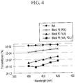
FIG. 4 illustrates a transmittance graph according to materials of a passivation layer and a pixel defining layer. -
FIG. 5 andFIG. 6 illustrate cross-sectional views of a light emitting diode display device according to an exemplary embodiment. -
FIG. 7 illustrates a layout view of a light emitting diode display device according to an exemplary embodiment. -
FIG. 8 illustrates a cross-sectional view taken along line VIII-VIII ofFIG. 7 . -
FIG. 9 illustrates a cross-sectional view of a light emitting diode display device according to an exemplary embodiment. -
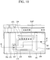
FIG. 10 illustrates a layout view of a light emitting diode display device according to an exemplary embodiment. -
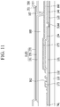
FIG. 11 illustrates a cross-sectional view taken along line XI-XI ofFIG. 10 . -
FIG. 12 illustrates a cross-sectional view of a light emitting diode display device according to an exemplary embodiment. -
FIG. 13 illustrates a layout view of a light emitting diode display device according to an exemplary embodiment. -
FIG. 14 illustrates a cross-sectional view taken along line XIV-XIV ofFIG. 13 . -
FIG. 15 illustrates a cross-sectional view of a light emitting diode display device according to an exemplary embodiment. -
FIG. 16 illustrates a layout view of a light emitting diode display device according to an exemplary embodiment. -
FIG. 17 illustrates a layout view of a light emitting diode display device according to an exemplary embodiment. -
FIG. 18 illustrates a schematic view of a light emitting diode display device according to an exemplary embodiment. -
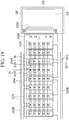
FIG. 19 illustrates a layout view of a thin film transistor included in a gate driver of a light emitting diode display device according to an exemplary embodiment. -
FIG. 20 illustrates a cross-sectional view taken along line XX-XX ofFIG. 19 . -
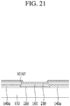
FIG. 21 illustrates a cross-sectional view taken along line XXI-XXI ofFIG. 19 . - The present invention will be described more fully hereinafter with reference to the accompanying drawings, in which exemplary embodiments of the invention are shown. As those skilled in the art would realize, the described embodiments may be modified in various different ways, all without departing from the scope of the present invention.
- To clearly describe the present invention, portions which do not relate to the description are omitted, and like reference numerals designate like elements throughout the specification.
- Further, the size and thickness of each component shown in the drawings are arbitrarily shown for better understanding and ease of description, but the present invention is not limited thereto. In the drawings, the thickness of layers, films, panels, regions, etc., are exaggerated for clarity. For better understanding and ease of description, the thickness of some layers and areas is exaggerated.
- It will be understood that when an element such as a layer, film, region, or substrate is referred to as being "on" another element, it may be directly on the other element, or intervening elements may also be present. In contrast, when an element is referred to as being "directly on" another element, there are no intervening elements present. Further, in the specification, the word "on" or "above" means positioned on or below the object portion, and does not necessarily mean positioned on the upper side of the object portion based on a gravitational direction.
- In addition, unless explicitly described to the contrary, the word "comprise" and variations such as "comprises" or "comprising" will be understood to imply the inclusion of stated elements but not the exclusion of any other elements.
- Throughout the specification, the phrase "on a plane" means viewing the object portion from the top, and the phrase "on a cross-section" means viewing a cross-section of which the object portion is vertically cut from the side.
- A light emitting diode display device according to an exemplary embodiment will be described with reference to
FIG. 1 to FIG. 3 . -
FIG. 1 illustrates a layout view of a light emitting diode display device according to an exemplary embodiment,FIG. 2 illustrates a cross-sectional view taken along line II-II ofFIG. 1 , andFIG. 3 illustrates a cross-sectional view taken along line III-III ofFIG. 1 . - As shown in
FIG. 1 to FIG. 3 , in the light emitting diode display device according to the exemplary embodiment, abuffer layer 120 is positioned on asubstrate 110. - The
substrate 110 may be an insulating substrate made of glass, quartz, ceramic, plastic, etc., or a metal substrate made of stainless steel and the like. - The
buffer layer 120 may include an inorganic or organic insulating material such as a silicon oxide (SiOx), a silicon nitride (SiNx), silicon oxynitride (SiON), silicon oxyfluoride (SiOF), an aluminum oxide (AlOx), etc., and it may be formed as a single layer or a multilayer including at least one of the materials. Thebuffer layer 120 serves to flatten a surface while preventing undesirable materials, such as impurities or moisture, from permeating. Thebuffer layer 120 may be positioned on most of a region of thesubstrate 110. Thebuffer layer 120 may be omitted in some cases. - A
semiconductor 135 is positioned on thebuffer layer 120. Thesemiconductor 135 may be made of a polycrystalline semiconductor material or an oxide semiconductor material. In addition, thesemiconductor 135 includes achannel region 131, and contactdoping regions channel region 131 and include impurities such as P-type impurities or N-type impurities. Thecontact doping regions - A
gate insulating layer 140 is positioned on thesemiconductor 135 and thebuffer layer 120. Thegate insulating layer 140 may include an inorganic insulating material or an organic insulating material such as a silicon oxide (SiOx), a silicon nitride (SiNx), silicon oxynitride (SiON), silicon oxyfluoride (SiOF), an aluminum oxide (AlOx), etc., and it may be formed as a single layer or a multilayer including at least one of the materials. - A
gate electrode 154 is positioned on thegate insulating layer 140. Thegate electrode 154 overlaps at least some of thesemiconductor 135, and particularly, thechannel region 131. - An interlayer insulating
layer 160 is positioned on thegate electrode 154, thesemiconductor 135, and thebuffer layer 120. The interlayer insulatinglayer 160 may include an inorganic insulating material or organic insulating material such as a silicon oxide (SiOx), a silicon nitride (SiNx), silicon oxynitride (SiON), silicon oxyfluoride (SiOF), an aluminum oxide (AlOx), etc., and it may be formed as a single layer or a multilayer including at least one of the materials. - Contact holes 162 and 164 overlapping at least some of the
semiconductor 135 are provided in theinterlayer insulating layer 160. The contact holes 162 and 164 expose thecontact doping regions semiconductor 135. - A
source electrode 173 and adrain electrode 175 are positioned on theinterlayer insulating layer 160. Thesource electrode 173 is connected to thesource region 132 of thesemiconductor 135 through thecontact hole 162. Thedrain electrode 175 is connected to thedrain region 133 of thesemiconductor 135 through thecontact hole 164. Thedrain electrode 175 may be formed to have an island shape. - The
semiconductor 135 overlaps thesource electrode 173 and thedrain electrode 175. In this case, most of thechannel region 131 of thesemiconductor 135 may overlap thedrain electrode 175. InFIG. 1 , thechannel region 131 of thesemiconductor 135 is entirely covered by thedrain electrode 175. - A driving
voltage line 172 and acommon voltage line 741 are further positioned on theinterlayer insulating layer 160. The drivingvoltage line 172 and thecommon voltage line 741 may extend in a direction parallel to each other, and they are adjacent to each other. A driving voltage (ELVDD) is applied to the drivingvoltage line 172. The drivingvoltage line 172 is connected to thesource electrode 173 to transmit the driving voltage (ELVDD) to thesource electrode 173. A common voltage (ELVSS) is applied to thecommon voltage line 741. -
Slits buffer layer 120 and the interlayer insulatinglayer 160, and theslits semiconductor 135 and thegate electrode 154. Theslits substrate 110. - The
slit 1165 overlaps thecommon voltage line 741. Thecommon voltage line 741 contacts thesubstrate 110 through theslit 1165. Theslit 1165 may have a bar shape in a plan view, and may extend in a direction substantially parallel to thecommon voltage line 741. For example, theslit 1165 may substantially extend in a vertical direction. Theslit 1165 is positioned at a left side of thesemiconductor 135 in a plan view, and it may be positioned to be adjacent to a left edge of thesemiconductor 135. Thecommon voltage line 741 is positioned in theslit 1165, and thecommon voltage line 741 may be made of an opaque metal material. Accordingly, light otherwise would be incident on left and right sides of thesemiconductor 135 may be blocked by thecommon voltage line 741 positioned in theslit 1165. - The
slits drain electrode 175. Thedrain electrode 175 contacts thesubstrate 110 through theslits slits common voltage line 741. For example, theslits slit 1166 may be positioned below thesemiconductor 135 in a plan view, and it may be positioned to be adjacent to a lower edge of thesemiconductor 135. Theslit 1167 may be positioned above thesemiconductor 135 in a plan view, and it may be formed to have a bar shape that is bent once (e.g., an L shape). In this case, most of theslit 1167 is positioned at an upper side of thesemiconductor 135, some of a remaining part thereof is positioned at a right side of thesemiconductor 135, and theslit 1167 may be positioned to be adjacent to upper and right edges of thesemiconductor 135. Thedrain electrode 175 is positioned in theslits drain electrode 175 may be made of an opaque metal material. Accordingly, light otherwise would be incident on upper and lower surfaces of thesemiconductor 135 may be blocked by thedrain electrode 175 positioned in theslits - As such, the light incident on a lateral surface of the
semiconductor 135 may be blocked by thecommon voltage line 741 and thedrain electrode 175 positioned in theslits semiconductor 135 is mostly covered by thesource electrode 173 and thedrain electrode 175, and thus light otherwise would be incident on the upper surface of thesemiconductor 135 may also be blocked. In the present exemplary embodiment, light incident on the upper and lateral surfaces of thesemiconductor 135 may be blocked by using thecommon voltage line 741, thedrain electrode 175, etc., and a separate light blocking material layer is not required. - Since a predetermined voltage is applied to the
common voltage line 741 and thedrain electrode 175, when different metal layers are exposed through theslits common voltage line 741 or thedrain electrode 175. Accordingly, in some embodiments, the different metal layers may not be positioned below theslits slits common voltage line 741 and thedrain electrode 175 may be disposed to contact thesubstrate 110, thebuffer layer 120, theinterlayer insulating layer 160, etc., through theslits gate electrode 154, etc. - The
semiconductor 135, thegate electrode 154, thesource electrode 173, and thedrain electrode 175 form one thin film transistor. A structure of the thin film transistor is not limited to the aforementioned example, and may be modified to a variety of disclosed structures that can be easily implemented by those skilled in the art. - A
passivation layer 180 is positioned on thesource electrode 173, thedrain electrode 175, thecommon voltage line 741, the drivingvoltage line 172, and the interlayer insulatinglayer 160. Thepassivation layer 180 serves to remove and flatten steps, thereby increasing luminous efficiency of the OLED to be formed thereon. Acontact hole 182 overlapping at least some of thedrain electrode 175 is formed in thepassivation layer 180. - The
passivation layer 180 may be made of a polyacrylate resin, an epoxy resin, a phenolic resin, a polyamide resin, a polyimide resin, an unsaturated polyester resin, a polyphenylene resin, a polyphenylene sulfide resin, and benzocyclobutene (BCB). - A
first electrode 191 is positioned on thepassivation layer 180. Thefirst electrode 191 may be made of a transparent conductive material such as indium tin oxide (ITO), indium zinc oxide (IZO), zinc oxide (ZnO), indium oxide (In2O3), etc., or a reflective metal such as lithium (Li), calcium (Ca), lithium fluoride/calcium (LiF/Ca), lithium fluoride/aluminum (LiF/Al), aluminum (Al), silver (Ag), magnesium (Mg), gold (Au), etc. Thefirst electrode 191 is electrically connected to thedrain electrode 175 of the thin film transistor via thecontact hole 182 formed in thepassivation layer 180, and becomes the anode of the OLED. - Although not illustrated, the
first electrode 191 may include first and second transparent electrodes including a transparent conductive material, and a semi-transmissive layer positioned between the first and second transparent electrodes to form a microcavity together with asecond electrode 270. That is, thefirst electrode 191 may be formed as a multilayer including a layer made of the transparent conductive material and a layer made of a reflective metal material. - A
pixel defining layer 350 is positioned on thepassivation layer 180 and on an edge portion of thefirst electrode 191. Thepixel defining layer 350 includes apixel opening 351 that does not cover thefirst electrode 191. Thepixel defining layer 350 surrounds edges of thefirst electrode 191. Thepixel defining layer 350 may include a resin such as a polyacrylate resin and a polyimide resin, or a silica-based inorganic material. - An
organic emission layer 370 is provided in thepixel opening 351 of thepixel defining layer 350. Theorganic emission layer 370 is formed as a multilayer including one or more of an emission layer, a hole-injection layer (HIL), a hole-transporting layer (HTL), an electron-transporting layer (ETL), and an electron-injection layer (EIL). In a case in which theorganic emission layer 370 includes all the layers, the hole-injection layer may be positioned on thefirst electrode 191 corresponding to an anode, and then the hole-transporting layer, the emission layer, the electron-transporting layer, and the electron-injection layer may be sequentially stacked thereon. - The
organic emission layer 370 may include a red organic emission layer for emitting red light, a green organic emission layer for emitting green light, and a blue organic emission layer for emitting blue light. The red organic emission layer, the green organic emission layer, and the blue organic emission layer are respectively formed on red, green, and blue pixels to implement a color image. - Alternatively, in the organic
light emission layer 370, a color image may be implemented by respectively stacking the red, green, and blue organic light emission layers on the red pixel, the green pixel, and the blue pixel, and then forming red, green, and blue color filters for each pixel. As another example, a color image may be implemented by forming a white organic emission layer emitting white light on all of the red, green, and blue pixels and respectively forming red, green, and blue color filters for each pixel. When the color image is implemented by using the white organic emission layer and the color filter, a deposition mask for depositing the red, green, and blue organic emission layers on each pixel, that is, the red, green, and blue pixels, is not required. - The white organic emission layer described in another exemplary embodiment may be formed as a single organic emission layer, and may further include a structure for emitting white light by laminating a plurality of organic emission layers. For example, a structure for emitting white light by combining at least one yellow organic emission layer with at least one blue organic emission layer, a structure for emitting white light by combining at least one cyan organic emission layer with at least one red organic emission layer, and a structure for emitting white light by combining at least one magenta organic emission layer with at least one green organic emission layer may be included.
- The
second electrode 270 is positioned on thepixel defining layer 350 and theorganic emission layer 370. Thesecond electrode 270 is connected to thecommon voltage line 741 to receive a common voltage. Thesecond electrode 270 may be made of a transparent conductive material such as indium tin oxide (ITO), indium zinc oxide (IZO), zinc oxide (ZnO), indium oxide (In2O3), etc., or a reflective metal such as lithium (Li), calcium (Ca), lithium fluoride/calcium (LiF/Ca), lithium fluoride/aluminum (LiF/Al), aluminum (Al), silver (Ag), magnesium (Mg), gold (Au), etc. Thesecond electrode 270 becomes the cathode of the organic light emitting diode (OLED). Thefirst electrode 191, theorganic emission layer 370, and thesecond electrode 270 form the organic light emitting diode (OLED). - The
organic emission layer 370 may be substituted with an emission layer made of an inorganic material. In this case, another light-emitting device may be used instead of the organic light emitting diode (OLED). For example, a quantum light emitting diode (QLED) and the like may be used. - Although most of the light generated from the organic light emitting diode (OLED) is emitted from an upper surface thereof, some of the light is emitted from a lateral surface thereof. The light emitted from the lateral surface of the organic light emitting diode (OLED) may be directed toward a thin film transistor of an adjacent pixel. In the present exemplary embodiment, the
slits semiconductor 135, and thecommon voltage line 741 and thedrain electrode 175 are positioned to overlap theslits semiconductor 135. Accordingly, it is possible to prevent characteristics of thesemiconductor 135 from being changed and to improve reliability of the thin film transistor. - In the present exemplary embodiment, the passivation layer and the pixel defining layer may be made of a transparent material. However, the present invention is not limited thereto, and in a light emitting diode display device according to another exemplary embodiment, the passivation layer or the pixel defining layer may be made of a light blocking material. A passivation layer and/or a pixel defining layer made of a light blocking material will be described with reference to
FIG. 4 . -
FIG. 4 illustrates a transmittance graph according to materials of a passivation layer and a pixel defining layer. - As shown in
FIG. 4 , in a case (hereinafter referred to as a 'reference') (Ref.) in which both the passivation layer and the pixel defining layer are made of the transparent material, transmittance thereof is highest. That is, in the reference (Ref.), an amount of light that passes through the passivation layer and the pixel defining layer and then reaches the thin film transistor may be a maximum. - In a case (hereinafter referred to as an 'A case') (Black PI (PDL)) in which the passivation layer is made of a transparent material and the pixel defining layer is made of an opaque material, transmittance thereof is lower than the reference (Ref.). That is, in the A case (Black PI (PDL)), an amount of light that passes through the passivation layer and the pixel defining layer and then reaches the thin film transistor may be smaller than that of the reference (Ref.).
- In a case (hereinafter, referred to as a 'B case') (Black PI (VIA)) in which the passivation layer is made of an opaque material and the pixel defining layer is made of a transparent material, transmittance thereof is lower than the reference (Ref.) and the A case (Black PI (PDL)). That is, in the B case (Black PI (VIA)), an amount of light that passes through the passivation layer and the pixel defining layer and then reaches the thin film transistor may be smaller than that of the reference (Ref.) and the A case (Black PI (PDL)).
- In a case (hereinafter referred to as a 'C case') (Black PI (VIA, PDL)) in which both the passivation layer and the pixel defining layer are made of an opaque material, transmittance thereof is lowest. That is, in the C case (Black PI (VIA, PDL)), an amount of light that passes through the passivation layer and the pixel defining layer and then reaches the thin film transistor may be a minimum.
- As described above, by making the passivation layer and/or the pixel defining layer of the light blocking material, it is possible to decrease an amount of light incident on the thin film transistor to prevent characteristics of the semiconductor from being changed, thereby improving reliability of the thin film transistor.
- Hereinafter, a light emitting diode display device according to an exemplary embodiment will be described with reference to
FIG. 5 andFIG. 6 . - The light emitting diode display device according to the exemplary embodiment shown in
FIG. 5 andFIG. 6 includes many portions that are the same as those in the light emitting diode display device according to the exemplary embodiment shown inFIG. 1 to FIG. 3 , which will not be described. In the present exemplary embodiment, a configuration in which the common voltage line and the drain electrode do not contact the substrate is different from that of the previous exemplary embodiments, and will now be described in detail. -
FIG. 5 andFIG. 6 illustrate cross-sectional views of a light emitting diode display device according to an exemplary embodiment. - As shown in
FIG. 5 andFIG. 6 , a light emitting diode display device according to an exemplary embodiment includes thesubstrate 110, thesemiconductor 135 positioned on thesubstrate 110, thegate electrode 154 positioned on thesemiconductor 135, theinterlayer insulating layer 160 positioned on thesubstrate 110 and thegate electrode 154, and thesource electrode 173 and thedrain electrode 175 positioned on theinterlayer insulating layer 160. -
Slits interlayer insulating layer 160, and theslits semiconductor 135 and thegate electrode 154. Thebuffer layer 120 is further positioned between thesubstrate 110 and thesemiconductor 135, and theslits buffer layer 120. Although the slits are provided in the buffer layer in the previous exemplary embodiment, the slits are not provided in the buffer layer in the present exemplary embodiment. - The
slit 2165 overlaps thecommon voltage line 741. Thecommon voltage line 741 may contact thebuffer layer 120 through theslit 2165, while it may not contact thesubstrate 110. Theslit 2165 may have a bar shape in a plan view, and may extend in the direction substantially parallel to thecommon voltage line 741. For example, theslit 2165 may substantially extend in a vertical direction. The above definition with respect to horizontal and vertical direction also applies here and in the further embodiments. Theslit 2165 is positioned at the left side of thesemiconductor 135 in a plan view, and it may be positioned to be adjacent to the left edge of thesemiconductor 135. Thecommon voltage line 741 is positioned in theslit 2165, and thecommon voltage line 741 may be made of an opaque metal material. Accordingly, light otherwise would be incident on a left surface of thesemiconductor 135 may be blocked by thecommon voltage line 741 positioned in theslit 2165. - The
slits drain electrode 175. Thedrain electrode 175 may contact thebuffer layer 120 through theslits substrate 110. Theslits common voltage line 741. For example, theslits slit 2166 may be positioned below thesemiconductor 135 in a plan view, and it may be positioned to be adjacent to the lower edge of thesemiconductor 135. Theslit 2167 may be positioned above thesemiconductor 135 in a plan view, and it may be formed to have a bar shape that is bent once. In this case, most of theslit 2167 is positioned at the upper side of thesemiconductor 135, some of a remaining part thereof is positioned at the right side of thesemiconductor 135, and theslit 2167 may be positioned to be adjacent to the upper and right edges of thesemiconductor 135. Thedrain electrode 175 is positioned in theslits drain electrode 175 may be made of an opaque metal material. Accordingly, light otherwise would be incident on upper and lower surfaces of thesemiconductor 135 may be blocked by thedrain electrode 175 positioned in theslits - As such, the light incident on the lateral surface of the
semiconductor 135 may be blocked by thecommon voltage line 741 and thedrain electrode 175 positioned in theslits - Since a predetermined voltage is applied to the
common voltage line 741 and thedrain electrode 175, when different metal layers are exposed through theslits common voltage line 741 and thedrain electrode 175. Accordingly, it is preferable that the different metal layers are not positioned below theslits slits - Hereinafter, a light emitting diode display device according to an exemplary embodiment will be described with reference to
FIG. 7 andFIG. 8 . - The light emitting diode display device according to the exemplary embodiment shown in
FIG. 7 andFIG. 8 includes many portions that are the same as those in the light emitting diode display device according to the exemplary embodiment shown inFIG. 1 to FIG. 3 , which will not be described. In the present exemplary embodiment, a configuration in which the driving voltage line and the source electrode contact the substrate is different from that of the previous exemplary embodiments, and will now be described in detail. -
FIG. 7 illustrates a layout view of a light emitting diode display device according to an exemplary embodiment, andFIG. 8 illustrates a cross-sectional view taken along line III-III ofFIG. 1 . - As shown in
FIG. 7 andFIG. 8 , a light emitting diode display device according to an exemplary embodiment includes thesubstrate 110, thesemiconductor 135 positioned on thesubstrate 110, thegate electrode 154 positioned on thesemiconductor 135, theinterlayer insulating layer 160 positioned on thesubstrate 110 and thegate electrode 154, and thesource electrode 173 and thedrain electrode 175 positioned on theinterlayer insulating layer 160. -
Slits interlayer insulating layer 160, and theslits semiconductor 135 and thegate electrode 154. Theslits substrate 110. - The
slit 3165 overlaps thecommon voltage line 741. Thecommon voltage line 741 contacts thesubstrate 110 through theslit 3165. - The
slits drain electrode 175. Thedrain electrode 175 contacts thesubstrate 110 through theslits - The
slit 3168 overlaps the drivingvoltage line 172 and thesource electrode 173. The drivingvoltage line 172 and thesource electrode 173 contact thesubstrate 110 through theslit 3168. Theslit 3168 may have a bar shape in a plan view, and may extend in a direction substantially parallel to the drivingvoltage line 172. For example, theslit 3168 may substantially extend in a vertical direction. Theslit 3168 is positioned at the left side of thesemiconductor 135 in a plan view, and it may be positioned to be adjacent to the left edge of thesemiconductor 135. The drivingvoltage line 172 is positioned in theslit 3168, and the drivingvoltage line 172 may be made of an opaque metal material. Accordingly, light otherwise would be incident on the left surface of thesemiconductor 135 may be blocked by the drivingvoltage line 172 positioned in theslit 3168. - As such, the light incident on the lateral surface of the
semiconductor 135 may be blocked by thecommon voltage line 741, thedrain electrode 175, and the drivingvoltage line 172 positioned in theslits semiconductor 135 is mostly covered by thesource electrode 173 and thedrain electrode 175, and thus light otherwise would be incident on the upper surface of thesemiconductor 135 may also be blocked. In the present exemplary embodiment, without adding a separate light blocking material layer, the light incident on the upper and lateral surfaces of thesemiconductor 135 may be blocked by using thecommon voltage line 741, thedrain electrode 175, the drivingvoltage line 172, thesource electrode 173, etc. - Since a predetermined voltage is applied to the
common voltage line 741, thedrain electrode 175, the drivingvoltage line 172, and thesource electrode 173, when different metal layers are exposed through theslits common voltage line 741, thedrain electrode 175, the drivingvoltage line 172, and thesource electrode 173. Accordingly, in some embodiments, the different metal layers are not positioned below theslits slits - Hereinafter, a light emitting diode display device according to an exemplary embodiment will be described with reference to
FIG. 9 . - The light emitting diode display device according to the exemplary embodiment shown in
FIG. 9 includes many portions that are the same as those in the light emitting diode display device according to the exemplary embodiment shown inFIG. 7 andFIG. 8 , which will not be described. In the present exemplary embodiment, a configuration in which the common voltage line, the drain electrode, the driving voltage line, and the source electrode do not contact the substrate is different from that of the previous exemplary embodiments, and will now be described in detail. -
FIG. 9 illustrates a cross-sectional view of a light emitting diode display device according to an exemplary embodiment. - As shown in
FIG. 9 , a light emitting diode display device according to an exemplary embodiment includes thesubstrate 110, thesemiconductor 135 positioned on thesubstrate 110, thegate electrode 154 positioned on thesemiconductor 135, theinterlayer insulating layer 160 positioned on thesubstrate 110 and thegate electrode 154, and thesource electrode 173 and thedrain electrode 175 positioned on theinterlayer insulating layer 160. -
Slits interlayer insulating layer 160, and theslits semiconductor 135 and thegate electrode 154. Thebuffer layer 120 is further positioned between thesubstrate 110 and thesemiconductor 135, and theslits buffer layer 120. Although the slit is provided in the buffer layer in the previous exemplary embodiment, the slit is not provided in the buffer layer in the present exemplary embodiment. - The
slit 4165 overlaps thecommon voltage line 741. Thecommon voltage line 741 may contact thebuffer layer 120 through theslit 4165, while it may not contact thesubstrate 110. - The
slit 4168 overlaps the drivingvoltage line 172 and thesource electrode 173. The drivingvoltage line 172 and thesource electrode 173 may contact thebuffer layer 120 through theslit 4168, while it may not contact thesubstrate 110. - Similarly, although not illustrated, the
drain electrode 175 may also contact thebuffer layer 120 through the slit, while it may not contact thesubstrate 110. - Hereinafter, a light emitting diode display device according to an exemplary embodiment will be described with reference to
FIG. 10 andFIG. 11 . - The light emitting diode display device according to the exemplary embodiment shown in
FIG. 10 andFIG. 11 includes many portions that are the same as those in the light emitting diode display device according to the exemplary embodiment shown inFIG. 1 to FIG. 3 , which will not be described. In the present exemplary embodiment, a configuration in which the gate electrode contacts the substrate is different from that of the previous exemplary embodiments, and will now be described in detail. -
FIG. 10 illustrates a layout view of a light emitting diode display device according to an exemplary embodiment, andFIG. 11 illustrates a cross-sectional view taken along line XI-XI ofFIG. 10 . - As shown in
FIG. 10 andFIG. 11 , a light emitting diode display device according to an exemplary embodiment includes thesubstrate 110, thesemiconductor 135 positioned on thesubstrate 110, thegate insulating layer 140 positioned on thesemiconductor 135, thegate electrode 154 positioned on thegate insulating layer 140, theinterlayer insulating layer 160 positioned on thesubstrate 110 and thegate electrode 154, and thesource electrode 173 and thedrain electrode 175 positioned on theinterlayer insulating layer 160. -
Slits buffer layer 120 and the interlayer insulatinglayer 160, and aslit 5168 is provided in thebuffer layer 120 andgate insulating layer 140. Theslits semiconductor 135. Theslits substrate 110. - The
slits drain electrode 175, while they do not overlap thegate electrode 154. Thedrain electrode 175 contacts thesubstrate 110 through theslits - The
slit 5168 overlaps thegate electrode 154. Thegate electrode 154 contacts thesubstrate 110 through theslit 5168. Theslit 5168 may have a bar shape in a plan view, and may extend in a direction substantially parallel to the drivingvoltage line 172. For example, theslit 5168 may substantially extend in a vertical direction. Theslit 5168 is positioned at the right side of thesemiconductor 135 in a plan view, and may be positioned to be adjacent to the right edges of thesemiconductor 135. Thegate electrode 154 is positioned in theslit 5168, and thegate electrode 154 may be made of an opaque metal material. Accordingly, light otherwise would be incident on a right surface of thesemiconductor 135 may be blocked by thegate electrode 154 positioned in theslit 5168. - As such, the light incident on the lateral surface of the
semiconductor 135 may be blocked by thedrain electrode 175 and thegate electrode 154 positioned in theslits semiconductor 135 is mostly covered by thesource electrode 173 and thedrain electrode 175, and thus light otherwise would be incident on the upper surface of thesemiconductor 135 may also be blocked. In the present exemplary embodiment, without adding a separate light blocking material layer, the light incident on the upper and lateral surfaces of thesemiconductor 135 may be blocked by using thedrain electrode 175, thegate electrode 154, thesource electrode 173, etc. - Since a predetermined voltage is applied to the
drain electrode 175 and thegate electrode 154, when different metal layers are exposed through theslits drain electrode 175 and thegate electrode 154. Accordingly, in some embodiments, the different metal layers are not positioned below theslits slits - Hereinafter, a light emitting diode display device according to an exemplary embodiment will be described with reference to
FIG. 12 . - The light emitting diode display device according to the exemplary embodiment shown in
FIG. 12 includes many portions that are the same as those in the light emitting diode display device according to the exemplary embodiment shown inFIG. 10 andFIG. 11 , which will not be described. In the present exemplary embodiment, a configuration in which the drain electrode and the gate electrode do not contact the substrate is different from that of the previous exemplary embodiments, and will now be described in detail. -
FIG. 12 illustrates a cross-sectional view of a light emitting diode display device according to an exemplary embodiment. - As shown in
FIG. 12 , a light emitting diode display device according to an exemplary embodiment includes thesubstrate 110, thesemiconductor 135 positioned on thesubstrate 110, thegate insulating layer 140 positioned on thesemiconductor 135, thegate electrode 154 positioned on thegate insulating layer 140, theinterlayer insulating layer 160 positioned on thesubstrate 110 and thegate electrode 154, and thesource electrode 173 and thedrain electrode 175 positioned on theinterlayer insulating layer 160. - A
slit 6168 is provided in thegate insulating layer 140, and theslit 6168 does not overlap thesemiconductor 135. Thebuffer layer 120 is further positioned between thesubstrate 110 and thesemiconductor 135, and theslit 6168 exposes thebuffer layer 120. Although the slit is provided in the buffer layer in the previous exemplary embodiment, the slit is not provided in the buffer layer in the present exemplary embodiment. - The
slit 6168 overlaps thegate electrode 154. Thegate electrode 154 contacts thebuffer layer 120 through theslit 6168, while it may not contact thesubstrate 110. - Similarly, although not illustrated, the
drain electrode 175 may also contact thebuffer layer 120 through the slit, while it may not contact thesubstrate 110. - Hereinafter, a light emitting diode display device according to an exemplary embodiment will be described with reference to
FIG. 13 andFIG. 14 . - The light emitting diode display device according to the exemplary embodiment shown in
FIG. 13 andFIG. 14 includes many portions that are the same as those in the light emitting diode display device according to the exemplary embodiment shown inFIG. 10 andFIG. 11 , which will not be described. In the present exemplary embodiment, a configuration in which the common voltage line contacts the substrate is different from that of the previous exemplary embodiments, and will now be described in detail. -
FIG. 13 illustrates a layout view of a light emitting diode display device according to an exemplary embodiment, andFIG. 14 illustrates a cross-sectional view taken along line XIV-XIV ofFIG. 13 . - As shown in
FIG. 13 andFIG. 14 , a light emitting diode display device according to an exemplary embodiment includes thesubstrate 110, thesemiconductor 135 positioned on thesubstrate 110, thegate insulating layer 140 positioned on thesemiconductor 135, thegate electrode 154 positioned on thegate insulating layer 140, theinterlayer insulating layer 160 positioned on thesubstrate 110 and thegate electrode 154, and thesource electrode 173 and thedrain electrode 175 positioned on theinterlayer insulating layer 160. -
Slits buffer layer 120 and the interlayer insulatinglayer 160, while aslit 7168 is provided in thebuffer layer 120 andgate insulating layer 140. Theslits semiconductor 135. Theslits substrate 110. - The
slit 7165 overlaps thecommon voltage line 741. Thecommon voltage line 741 contacts thesubstrate 110 through theslit 7165. - The
slits drain electrode 175. Thedrain electrode 175 contacts thesubstrate 110 through theslits - The
slit 7168 overlaps thegate electrode 154. Thegate electrode 154 contacts thesubstrate 110 through theslit 7168. - As such, the light incident on the lateral surface of the
semiconductor 135 may be blocked by thecommon voltage line 741, thedrain electrode 175, and thegate electrode 154 positioned in theslits semiconductor 135 is mostly covered by thesource electrode 173 and thedrain electrode 175, and thus light incident otherwise would be on the upper surface of thesemiconductor 135 may also be blocked. In the present exemplary embodiment, without adding a separate light blocking material layer, the light incident on the upper and lateral surfaces of thesemiconductor 135 may be blocked by using thecommon voltage line 741, thedrain electrode 175, thegate electrode 154, and thesource electrode 173, etc.. - Since a predetermined voltage is applied to the
common voltage line 741, thedrain electrode 175, and thegate electrode 154, when different metal layers are exposed through theslits common voltage line 741, thedrain electrode 175, and thegate electrode 154. Accordingly, in some embodiments, the different metal layers are not positioned below theslits slits - Hereinafter, a light emitting diode display device according to an exemplary embodiment will be described with reference to
FIG. 15 . - The light emitting diode display device according to the exemplary embodiment shown in
FIG. 15 includes many portions that are the same as those in the light emitting diode display device according to the exemplary embodiment shown inFIG. 13 andFIG. 14 , which will not be described. In the present exemplary embodiment, a configuration in which the common voltage line, the drain electrode, and the gate electrode do not contact the substrate is different from that of the previous exemplary embodiments, and will now be described in detail. -
FIG. 15 illustrates a cross-sectional view of a light emitting diode display device according to an exemplary embodiment. - As shown in
FIG. 15 , a light emitting diode display device according to an exemplary embodiment includes thesubstrate 110, thesemiconductor 135 positioned on thesubstrate 110, thegate insulating layer 140 positioned on thesemiconductor 135, thegate electrode 154 positioned on thegate insulating layer 140, theinterlayer insulating layer 160 positioned on thesubstrate 110 and thegate electrode 154, and thesource electrode 173 and thedrain electrode 175 positioned on theinterlayer insulating layer 160. - A
slit 8165 is provided in theinterlayer insulating layer 160, and aslit 8168 is provided in thegate insulating layer 140. Theslits semiconductor 135. Thebuffer layer 120 is further positioned between thesubstrate 110 and thesemiconductor 135, and theslits buffer layer 120. Although the slit is provided in the buffer layer in the previous exemplary embodiment, the slit is not provided in the buffer layer in the present exemplary embodiment. - The
slit 8165 overlaps thecommon voltage line 741. Thecommon voltage line 741 contacts thebuffer layer 120 through theslit 8165, while it may not contact thesubstrate 110. - The
slit 8168 overlaps thegate electrode 154. Thegate electrode 154 contacts thebuffer layer 120 through theslit 8168, while it may not contact thesubstrate 110. - Similarly, although not illustrated, the
drain electrode 175 may also contact thebuffer layer 120 through the slit, while it may not contact thesubstrate 110. - Hereinafter, a light emitting diode display device according to an exemplary embodiment will be described with reference to
FIG. 16 . -
FIG. 16 illustrates a layout view of a light emitting diode display device according to an exemplary embodiment. - As shown in
FIG. 16 , a light emitting diode display device according to an exemplary embodiment includes a substrate (not shown), and a first thin film transistor (Ta), a second thin film transistor (Tb), a third thin film transistor (Tc), and afirst electrode 191 that are positioned on the substrate. In addition, the light emitting diode display device according to the exemplary embodiment may further include thecommon voltage line 741, the drivingvoltage line 172, a data line 171, and a sensing line 176. - The first thin film transistor (Ta) includes a
first gate electrode 1154a, afirst semiconductor 1135a, afirst source electrode 1173a, and afirst drain electrode 1175a. Thefirst source electrode 1173a is connected to the drivingvoltage line 172. Thefirst semiconductor 1135a overlaps thefirst gate electrode 1154a. Some region of thefirst semiconductor 1135a is connected to thefirst source electrode 1173a, and some other region of thefirst semiconductor 1135a is connected to thefirst drain electrode 1175a. The first thin film transistor (Ta) may be a driving thin film transistor. - The second thin film transistor (Tb) includes a
second gate electrode 1154b, asecond semiconductor 1135b, asecond source electrode 1173b, and asecond drain electrode 1175b. Thesecond source electrode 1173b is connected to the data line 171. Thesecond semiconductor 1135b overlaps thesecond gate electrode 1154b. Some region of thesecond semiconductor 1135b is connected to thesecond source electrode 1173b, and some other region of thesecond semiconductor 1135b is connected to thesecond drain electrode 1175b. Thesecond drain electrode 1175b is connected to thefirst gate electrode 1154a. The second thin film transistor (Tb) may be a switching thin film transistor. - The third thin film transistor (Tc) includes a
third gate electrode 1154c, athird semiconductor 1135c, athird source electrode 1173c, and athird drain electrode 1175c. Thethird source electrode 1173c is connected to the sensing line 176. Thethird semiconductor 1135c overlaps thethird gate electrode 1154c. Some region of thethird semiconductor 1135c is connected to thethird source electrode 1173c, and some other region of thethird semiconductor 1135c is connected to thethird drain electrode 1175c. Thethird drain electrode 1175c is connected to thefirst drain electrode 1175a. The third thin film transistor (Tc) may be a sensing switching thin film transistor. - The
first electrode 191 is formed to have a substantially quadrangular shape, and overlaps the first thin film transistor (Ta), the second thin film transistor (Tb), and the third thin film transistor (Tc). Particularly, thefirst electrode 191 overlaps most regions of thefirst semiconductor 1135a, thesecond semiconductor 1135b, and thethird semiconductor 1135c. Thefirst electrode 191 may include a reflective metal material. Accordingly, since thefirst electrode 191 covers most regions of thefirst semiconductor 1135a, thesecond semiconductor 1135b, and thethird semiconductor 1135c, light incident on upper surfaces of thefirst semiconductor 1135a, thesecond semiconductor 1135b, and thethird semiconductor 1135c may be blocked. - Hereinafter, a light emitting diode display device according to an exemplary embodiment will be described with reference to
FIG. 17 . - The light emitting diode display device according to the exemplary embodiment shown in
FIG. 17 includes many portions that are the same as those in the light emitting diode display device according to the exemplary embodiment shown inFIG. 16 , which will not be described. In the present exemplary embodiment, a configuration in which slits overlapping the common voltage line, the driving voltage line, and the first gate electrode are further formed is different from that of the previous exemplary embodiments, and will now be described in detail. -
FIG. 17 illustrates a layout view of a light emitting diode display device according to an exemplary embodiment. - As shown in
FIG. 17 , a light emitting diode display device according to an exemplary embodiment includes a substrate (not shown), and a first thin film transistor (Ta), a second thin film transistor (Tb), a third thin film transistor (Tc), and afirst electrode 191 that are positioned on the substrate. In addition, the light emitting diode display device according to the exemplary embodiment may further include thecommon voltage line 741, the drivingvoltage line 172, the data line 171, and the sensing line 176. - The interlayer insulating layer (not shown) may be positioned between the substrate and the
common voltage line 741 and between the substrate and the drivingvoltage line 172.Slits first gate electrode 1154a. Aslit 9167 is provided in the gate insulating layer. - The
slit 9165 overlaps thecommon voltage line 741. Thecommon voltage line 741 contacts the substrate through theslit 9165. - The
slit 9168 overlaps the drivingvoltage line 172. The drivingvoltage line 172 contacts the substrate through theslit 9168. - The
slit 9167 overlaps thefirst gate electrode 1154a. Thefirst gate electrode 1154a contacts the substrate through theslit 9167. - As in another exemplary embodiment previously described, the buffer layer may be further positioned below the interlayer insulating layer and the gate insulating layer. The
slits slits common voltage line 741, the drivingvoltage line 172, and thefirst gate electrode 1154a do not contact the substrate, while they contact the buffer layer. - Hereinafter, a light emitting diode display device according to an exemplary embodiment will be described with reference to
FIG. 18 to FIG. 21 . -
FIG. 18 illustrates a schematic view of a light emitting diode display device according to an exemplary embodiment,FIG. 19 illustrates a layout view of a thin film transistor included in a gate driver of a light emitting diode display device according to an exemplary embodiment,FIG. 20 illustrates a cross-sectional view taken along line XX-XX ofFIG. 19 , andFIG. 21 illustrates a cross-sectional view taken along line XXI-XXI ofFIG. 19 . - As shown in
FIG. 18 , a light emitting diode display device according to an exemplary embodiment includes adisplay panel 300, adata driver 460, agate driver 500, asignal controller 600, etc. - The
display panel 300 includes a display area (DA) displaying an image, and a peripheral area (PA) surrounding the display area (DA). Thegate driver 500 for applying gate voltages to gate lines (G1 to Gn) is disposed in the peripheral area (PA). - Data lines (D1 to Dm) of the display area (DA) may receive data voltages from the
data driver 460. In this case, thedata driver 460 may be an integrated circuit (IC) disposed on a flexible printed circuit board (FPCB) 450 attached to thedisplay panel 300. - The
gate driver 500 and thedata driver 460 are controlled by thesignal controller 600. A printed circuit board (PCB) 400 is positioned at the outside of the flexible printedcircuit board 450 and configured to transmit a signal from thesignal controller 600 to thedata driver 460 and thegate driver 500. - The signal transmitted to the
gate driver 500 from thesignal controller 600 through a plurality of signal lines SL may include a signal such as a vertical start signal, a clock signal, and a low voltage signal of a predetermined level. - A plurality of pixels PX may be disposed in the display area (DA), and the plurality of gate lines (G1 to Gn) and the plurality of data lines (D1 to Dm) may cross while being insulated from each other.
- The data lines (D1 to Dm) receive the data voltages from the
data driver 460, and the gate lines (G1 to Gn) receive gate voltages from thegate driver 500. - The
data driver 460 may be positioned on an upper or lower side of thedisplay panel 300 and connected to the data lines (D1 to Dm) extending in a vertical direction. - The
gate driver 500 receives a vertical start signal, a clock signal, and a low voltage corresponding to a gate-off voltage, and generates gate voltages (a gate-on voltage and a gate-off voltage) and applies them to the gate lines (G1 to Gn). - The
gate driver 500 may include a plurality of stages for generating and outputting gate voltages through the signals, and each stage may include a plurality of thin film transistors. Thegate driver 500 may be integrated in the peripheral area (PA) of thedisplay panel 300. - As shown in
FIG. 19 to FIG. 21 , a gate driver of a light emitting diode display device according to an exemplary embodiment may include the thin film transistor (TR) and a capacitor (CAP). - A plurality of thin film transistors (TR) may be disposed in one gate driver. The plurality of thin film transistors (TR) may be disposed in a matrix form.
- The capacitor (CAP) may be disposed at end portions of the plurality of thin film transistors (TR). In the present exemplary embodiment, the capacitor (CAP) is disposed at right end portions of the plurality of thin film transistors (TR). Although not illustrated, the display area (DA) of the
display panel 300 may be disposed at a right side of the capacitor (CAP). That is, the capacitor (CAP) may be disposed between the plurality of thin film transistors (TR) and the display area (DA). However, a position of the capacitor (CAP) is not limited thereto, and the capacitor (CAP) may be disposed at left end portions of the plurality of thin film transistors (TR). Thus, the plurality of thin film transistors (TR) may be disposed between the capacitor (CAP) and the display area (DA). - The thin film transistor (TR) includes a
lower gate electrode 2124, asemiconductor 2135, anupper gate electrode 2154, asource electrode 2173, and adrain electrode 2175. - The
lower gate electrode 2124 is positioned on thesubstrate 110. Thelower gate electrode 2124 may overlap some of thesemiconductor 2135. Thelower gate electrode 2124 may block light that passes through thesubstrate 110 from being incident on thesemiconductor 2135. - A first insulating
layer 140a may be positioned thelower gate electrode 2124. The first insulatinglayer 140a may include an inorganic insulating material or organic insulating material such as a silicon oxide (SiOx), a silicon nitride (SiNx), silicon oxynitride (SiON), silicon oxyfluoride (SiOF), an aluminum oxide (AlOx), etc., and it may be formed as a single layer or a multilayer including at least one of the materials. - The
semiconductor 2135 is positioned on the first insulatinglayer 140a. Thesemiconductor 2135 may overlap some of thelower gate electrode 2124 in a direction perpendicular to thesubstrate 110. Thesemiconductor 2135 may be made of an oxide semiconductor material. For example, thesemiconductor 2135 may be an indium-gallium-zinc oxide (IGZO) or an indium-tin-zinc oxide (ITZO). - A second insulating
layer 140b may be positioned thesemiconductor 2135. The secondinsulating layer 140b may include an inorganic insulating material or organic insulating material such as a silicon oxide (SiOx), a silicon nitride (SiNx), silicon oxynitride (SiON), silicon oxyfluoride (SiOF), an aluminum oxide (AlOx), etc., and it may be formed as a single layer or a multilayer including at least one of the materials. - The
upper gate electrode 2154 is positioned on the second insulatinglayer 140b. Theupper gate electrode 2154 overlaps thesemiconductor 2135 with the second insulatinglayer 140b therebetween. Theupper gate electrode 2154 may be electrically connected to thelower gate electrode 2124. Aslit 10163 may be provided in the first insulatinglayer 140a. Theupper gate electrode 2154 may be connected to thelower gate electrode 2124 through theslit 10163 to have a dual gate structure. - An interlayer insulating
layer 160 is positioned on theupper gate electrode 2154. The interlayer insulatinglayer 160 may include an inorganic insulating material or organic insulating material such as a silicon oxide (SiOx), a silicon nitride (SiNx), silicon oxynitride (SiON), silicon oxyfluoride (SiOF), an aluminum oxide (AlOx), etc., and it may be formed as a single layer or a multilayer including at least one of the materials. - The
source electrode 2173 and thedrain electrode 2175 are positioned on theinterlayer insulating layer 160. Thesource electrode 2173 may include a first portion that extends in a substantially horizontal direction, and a second portion that protrudes from the first portion and extends in a substantially vertical direction to overlap thesemiconductor 2135. Thedrain electrode 2175 may include a first portion that extends in a substantially horizontal direction, and a second portion that protrudes from the first portion and extends in a substantially vertical direction to overlap thesemiconductor 2135. Thesource electrode 2173 protrudes toward thedrain electrode 2175, and thedrain electrode 2175 protrudes toward thesource electrode 2173. -
Slits interlayer insulating layer 160. Theslit 10162 overlaps thesource electrode 2173 and thesemiconductor 2135. Thesource electrode 2173 is connected to thesemiconductor 2135 through theslit 10162. Theslit 10164 overlaps thedrain electrode 2175 and thesemiconductor 2135. Thedrain electrode 2175 is connected to thesemiconductor 2135 through theslit 10164. -
Slits layer 140a and the interlayer insulatinglayer 160. Theslits semiconductor 2135, thelower gate electrode 2124, and theupper gate electrode 2154. Theslits substrate 110. - The
slit 10165 overlaps thesource electrode 2173. Thesource electrode 2173 contacts thesubstrate 110 through theslit 10165. Theslit 10165 may have a bar shape in a plan view, and may extend in a direction substantially parallel to thesource electrode 2173. For example, theslit 10165 may substantially extend in a horizontal direction. Theslit 10165 is positioned at an upper side of anuppermost semiconductor 2135 in a plan view, and may be positioned to be adjacent to an upper edge of theuppermost semiconductor 2135. Thesource electrode 2173 is positioned in theslit 10165, and thesource electrode 2173 may be made of an opaque metal material. Accordingly, light otherwise would be incident on an upper surface of thesemiconductor 2135 may be blocked by thesource electrode 2173 positioned in theslit 10165. - The
slit 10166 overlaps thedrain electrode 2175. Thedrain electrode 2175 contacts thesubstrate 110 through theslit 10166. Theslit 10166 may have a bar shape in a plan view, and may extend in a direction substantially parallel to thedrain electrode 2175. For example, theslit 10166 may substantially extend in a horizontal direction. Theslit 10166 is positioned at a lower side of alowermost semiconductor 2135 in a plan view, and may be positioned to be adjacent to a lower edge of the lower side of alowermost semiconductor 2135. Thedrain electrode 2175 is positioned in theslit 10166, and thedrain electrode 2175 may be made of an opaque metal material. Accordingly, light otherwise would be incident on a lower surface of thesemiconductor 2135 may be blocked by thedrain electrode 2175 positioned in theslit 10166. - The capacitor (CAP) includes a
first capacitor electrode 210, theinterlayer insulating layer 160, and asecond capacitor electrode 230. - The
first capacitor electrode 210 is positioned on the first insulatinglayer 140a, and is electrically connected to theupper gate electrode 2154. Thefirst capacitor electrode 210 may be positioned at the same layer as theupper gate electrode 2154, and may be made of the same material as that theupper gate electrode 2154. - The
second capacitor electrode 230 is positioned to overlap thefirst capacitor electrode 210. The interlayer insulatinglayer 160 is positioned between thefirst capacitor electrode 210 and thesecond capacitor electrode 230. The interlayer insulatinglayer 160 may serve as a dielectric material. Thesecond capacitor electrode 230 is electrically connected to thedrain electrode 2175. Thesecond capacitor electrode 230 may be positioned at the same layer as thesource electrode 2173 and thedrain electrode 2175, and may be made of the same material as that of thesource electrode 2173 and thedrain electrode 2175. - A
slit 10167 is further provided in the first insulatinglayer 140a. Theslit 10167 does not overlap thesemiconductor 2135. Theslit 10167 exposes thesubstrate 110. - The
slit 10167 overlaps thefirst capacitor electrode 210. Thefirst capacitor electrode 210 contacts thesubstrate 110 through theslit 10167. Theslit 10167 may have a bar shape in a plan view, and may substantially extend in a vertical direction. Theslit 10167 is positioned at right sides ofsemiconductors 2135 in a plan view, and may be positioned to be adjacent to right edges of thesemiconductors 2135. Thefirst capacitor electrode 210 is positioned in theslit 10167, and thefirst capacitor electrode 210 may be made of an opaque metal material. Accordingly, light otherwise would be incident on a lateral surface of thesemiconductor 2135 may be blocked by thefirst capacitor electrode 210 positioned in theslit 10167. - As such, light otherwise would be incident on a lateral surface of the
semiconductor 2135 may be blocked by thesource electrode 2173, thedrain electrode 2175, and thefirst capacitor electrode 210 that are positioned in theslits semiconductor 2135 is mostly covered by thesource electrode 2173, thedrain electrode 2175, and theupper gate electrode 2154, light otherwise would be incident on the upper surface of thesemiconductor 2135 may also be blocked. In the present exemplary embodiment, without adding a separate light blocking material layer, light otherwise would be incident on the upper and lateral surfaces of thesemiconductor 2135 may be blocked by using thesource electrode 2173, thedrain electrode 2175, thefirst capacitor electrode 210, etc. - Since a predetermined voltage is applied to the
source electrode 2173, thedrain electrode 2175, and thefirst capacitor electrode 210, when different metal layers are exposed through theslits source electrode 2173, thedrain electrode 2175, and thefirst capacitor electrode 210. Accordingly, in some embodiments, the different metal layers are not positioned below theslits slits - As in another exemplary embodiment previously described, the buffer layer may be further positioned below the
interlayer insulating layer 160 and the first insulatinglayer 140a. Theslits slits interlayer insulating layer 160 and the first insulatinglayer 140a. In this case, thesource electrode 2173, thedrain electrode 2175, and thefirst capacitor electrode 210 do not contact thesubstrate 110, while they contact the buffer layer. - While this disclosure has been described in connection with exemplary embodiments, it is to be understood that the invention is not limited to the disclosed embodiments, but, on the contrary, is intended to cover various modifications and equivalent arrangements included within the scope of the appended claims.
Claims (15)
- A light emitting diode display device, comprising:a substrate (110);a semiconductor (135,1135,2135) disposed on the substrate (110);a gate electrode (154, 2124) disposed on the semiconductor (135,1135,2135);an interlayer insulating layer (160) disposed on the substrate (110) and the gate electrode (154, 2124);source and drain electrodes (173, 1173, 2173, 175, 1175, 2175) disposed on the interlayer insulating layer (160) and connected to the semiconductor (135,1135,2135);at least a first slit (1165-1167, 2165-2167, 3165-3168,..,10162-10167) provided in the interlayer insulating layer (160); andat least a first wire disposed on the interlayer insulating layer (160) and configured to overlap the first slit (1165-1167, 2165-2167, 3165-3168,..,10162-10167).
- The light emitting diode display device of claim 1, wherein
the first wire contacts the substrate (110) through the first slit. - The light emitting diode display device of claim 1 or 2, wherein
the first wire is disposed at the same layer as the source electrode (173, 1173, 2173) and the drain electrode (175, 1175, 2175), and is made of the same material as that of the source electrode (173,1173,2173) and the drain electrode (175,1175, 2175). - The light emitting diode display device of at least one of claims 1 to 3,
wherein
the first wire is a common voltage line (741). - The light emitting diode display device of at least one of claims 1 to 3,
wherein
the first wire is a driving voltage line (172) connected to the source electrode (173,1173, 2173). - The light emitting diode display device of at least one of claims 1 to 5,
wherein
the first slit is adjacent to an edge of one side of the semiconductor (135, 1135, 2135), and does not overlap the semiconductor (135,1135,2135). - The light emitting diode display device of at least one of claims 1 to 6,
wherein
the first slit has a bar shape extending in a first direction. - The light emitting diode display device of at least one of claims 1 to 7,
wherein
the first slit extends in a direction parallel to the first wire. - The light emitting diode display device of at least one of claims 1 to 8, further comprising
a second slit provided in the interlayer insulating layer (160),
wherein the drain electrode (175,1175,2175) overlaps the second slit. - The light emitting diode display device of claim 9, wherein
the drain electrode (175, 1175, 2175) contacts the substrate (110) through the second slit. - The light emitting diode display device of claim 9 or 10, wherein
the second slit is adjacent to an edge of one side of the semiconductor (135, 1135, 2135), and does not overlap the semiconductor (135,1135, 2135), and
wherein the second slit extends in a direction crossing a direction in which the first wire extends. - The light emitting diode display device of at least one of claims 1 to 11, further comprising
a buffer layer (120) disposed between the substrate (110) and the interlayer insulating layer (160),
wherein the first wire contacts the buffer layer (120) through the first slit. - The light emitting diode display device of at least one of claims 1 to 12, further comprising:a third slit provided in the interlayer insulating layer (160); anda second wire positioned on the interlayer insulating layer (160), and configured to overlap the third slit, andwherein the second wire is connected to the substrate (110) through the third slit.
- The light emitting diode display device of at least one of claims 1 to 13, further comprising:a gate insulating layer (140) disposed between the substrate (110) and the gate electrode (154, 2124); anda fourth slit provided in the gate insulating layer (140),wherein the gate electrode (154, 2124) overlaps the fourth slit, andwherein the gate electrode (154, 2124) is connected to the substrate (110) through the fourth slit.
- The light emitting diode display device of at least one of claims 1 to 14, further comprising
a first electrode (191) connected to the drain electrode (175,1175, 2175),
wherein the first electrode (191) covers most of the semiconductor (135, 1135, 2135), and
wherein the first electrode (191) covers all of the semiconductor (135, 1135, 2135), the source electrode (173, 1173, 2173), the drain electrode (175, 1175, 2175), the gate electrode (154, 2124), and the first wire.
Applications Claiming Priority (1)
| Application Number | Priority Date | Filing Date | Title |
|---|---|---|---|
| KR1020160120119A KR102573853B1 (en) | 2016-09-20 | 2016-09-20 | Light emitting diode display device |
Publications (2)
| Publication Number | Publication Date |
|---|---|
| EP3297028A1 true EP3297028A1 (en) | 2018-03-21 |
| EP3297028B1 EP3297028B1 (en) | 2023-01-11 |
Family
ID=59955368
Family Applications (1)
| Application Number | Title | Priority Date | Filing Date |
|---|---|---|---|
| EP17191903.8A Active EP3297028B1 (en) | 2016-09-20 | 2017-09-19 | Light emitting diode display device |
Country Status (4)
| Country | Link |
|---|---|
| US (2) | US10665655B2 (en) |
| EP (1) | EP3297028B1 (en) |
| KR (1) | KR102573853B1 (en) |
| CN (1) | CN107845660B (en) |
Families Citing this family (5)
| Publication number | Priority date | Publication date | Assignee | Title |
|---|---|---|---|---|
| KR102642017B1 (en) * | 2016-11-30 | 2024-02-28 | 엘지디스플레이 주식회사 | Organic light emitting display device |
| US10971527B2 (en) * | 2018-09-11 | 2021-04-06 | Sharp Kabushiki Kaisha | Thin-film transistor substrate including data line with lower layer data line and upper layer data line, and liquid crystal display device and organic electroluminescent display device including same |
| CN109616497A (en) * | 2018-11-30 | 2019-04-12 | 武汉华星光电技术有限公司 | OLED display panel |
| US11289673B2 (en) * | 2019-08-06 | 2022-03-29 | Wuhan China Star Optoelectronics Semiconductor Display Technology Co., Ltd. | Display panel having Bragg mirror and manufacturing method of same |
| JP7782462B2 (en) * | 2020-12-11 | 2025-12-09 | ソニーグループ株式会社 | Light-emitting device manufacturing method |
Citations (4)
| Publication number | Priority date | Publication date | Assignee | Title |
|---|---|---|---|---|
| US20020101152A1 (en) * | 2001-01-30 | 2002-08-01 | Semiconductor Energy Laboratory Co., Ltd. | Light emitting device |
| JP2003084687A (en) * | 2001-05-23 | 2003-03-19 | Semiconductor Energy Lab Co Ltd | Semiconductor device and method of fabricating the same |
| US20030116768A1 (en) * | 2001-05-23 | 2003-06-26 | Semiconductor Energy Laboratory Co., Ltd. | Semiconductor device and manufacturing method thereof |
| US20050168135A1 (en) * | 2003-12-16 | 2005-08-04 | Nec Corporation | Luminescence display apparatus and method for fabricating the same |
Family Cites Families (25)
| Publication number | Priority date | Publication date | Assignee | Title |
|---|---|---|---|---|
| US6825496B2 (en) * | 2001-01-17 | 2004-11-30 | Semiconductor Energy Laboratory Co., Ltd. | Light emitting device |
| KR100761077B1 (en) * | 2005-05-12 | 2007-09-21 | 삼성에스디아이 주식회사 | Organic electroluminescent display |
| KR101424784B1 (en) | 2006-01-10 | 2014-07-31 | 가부시키가이샤 한도오따이 에네루기 켄큐쇼 | Display device and manufacturing method thereof |
| JP4930704B2 (en) * | 2006-03-14 | 2012-05-16 | セイコーエプソン株式会社 | Organic electroluminescence device and electronic device |
| KR20070115221A (en) | 2006-06-01 | 2007-12-05 | 삼성전자주식회사 | Thin film transistor array panel and manufacturing method thereof |
| KR100824881B1 (en) | 2006-11-10 | 2008-04-23 | 삼성에스디아이 주식회사 | Organic electroluminescent display and manufacturing method thereof |
| WO2009157531A1 (en) * | 2008-06-27 | 2009-12-30 | 株式会社日立製作所 | Semiconductor device, manufacturing method thereof, and display device using the semiconductor device |
| JP2010015019A (en) * | 2008-07-04 | 2010-01-21 | Hitachi Displays Ltd | Liquid crystal display device and manufacturing method for the same |
| WO2010032602A1 (en) * | 2008-09-18 | 2010-03-25 | Semiconductor Energy Laboratory Co., Ltd. | Semiconductor device |
| KR101592012B1 (en) | 2008-12-01 | 2016-02-05 | 삼성디스플레이 주식회사 | Organic light emitting device and manufacturing method thereof |
| JP2011071476A (en) | 2009-08-25 | 2011-04-07 | Canon Inc | Thin film transistor, display device using the same, and method of manufacturing thin film transistor |
| KR101084176B1 (en) | 2009-11-26 | 2011-11-17 | 삼성모바일디스플레이주식회사 | Organic light emitting display device |
| KR101234228B1 (en) | 2010-06-04 | 2013-02-18 | 삼성디스플레이 주식회사 | Organic light emitting display apparatus |
| KR20120078293A (en) | 2010-12-31 | 2012-07-10 | 삼성전자주식회사 | Transistor, method of manufacturing the same and electronic device comprising transistor |
| KR101809661B1 (en) * | 2011-06-03 | 2017-12-18 | 삼성디스플레이 주식회사 | Thin film transistor, manufacturing method of thin film transistor, and organic light emitting diode display including the same |
| KR20130111872A (en) * | 2012-04-02 | 2013-10-11 | 삼성디스플레이 주식회사 | Thin film transistor, thin film transistor array panel including the same and manufacturing method thereof |
| JP6044358B2 (en) * | 2013-01-18 | 2016-12-14 | セイコーエプソン株式会社 | Electro-optical device substrate, electro-optical device, and electronic apparatus |
| KR102083432B1 (en) | 2013-05-30 | 2020-03-03 | 삼성디스플레이 주식회사 | Organic light emitting diode display |
| KR102192592B1 (en) * | 2013-07-22 | 2020-12-18 | 삼성디스플레이 주식회사 | Organic light emitting diode display |
| JP2016001712A (en) * | 2013-11-29 | 2016-01-07 | 株式会社半導体エネルギー研究所 | Method of manufacturing semiconductor device |
| JP6277376B2 (en) * | 2014-01-29 | 2018-02-14 | 株式会社Joled | Image display device |
| JP6140626B2 (en) * | 2014-03-03 | 2017-05-31 | 富士フイルム株式会社 | Organic thin film transistor and manufacturing method thereof |
| KR20150142139A (en) * | 2014-06-10 | 2015-12-22 | 삼성디스플레이 주식회사 | Thin film transistor array substrate and method for manufacturing of the same |
| CN105390502B (en) * | 2014-08-29 | 2019-07-12 | 乐金显示有限公司 | Display device |
| KR102556162B1 (en) * | 2016-08-31 | 2023-07-19 | 엘지디스플레이 주식회사 | Thin film Transistor Substrate For Flat Panel Display |
-
2016
- 2016-09-20 KR KR1020160120119A patent/KR102573853B1/en active Active
-
2017
- 2017-09-18 US US15/707,637 patent/US10665655B2/en active Active
- 2017-09-19 EP EP17191903.8A patent/EP3297028B1/en active Active
- 2017-09-20 CN CN201710851843.6A patent/CN107845660B/en active Active
-
2020
- 2020-05-22 US US16/882,260 patent/US11574975B2/en active Active
Patent Citations (4)
| Publication number | Priority date | Publication date | Assignee | Title |
|---|---|---|---|---|
| US20020101152A1 (en) * | 2001-01-30 | 2002-08-01 | Semiconductor Energy Laboratory Co., Ltd. | Light emitting device |
| JP2003084687A (en) * | 2001-05-23 | 2003-03-19 | Semiconductor Energy Lab Co Ltd | Semiconductor device and method of fabricating the same |
| US20030116768A1 (en) * | 2001-05-23 | 2003-06-26 | Semiconductor Energy Laboratory Co., Ltd. | Semiconductor device and manufacturing method thereof |
| US20050168135A1 (en) * | 2003-12-16 | 2005-08-04 | Nec Corporation | Luminescence display apparatus and method for fabricating the same |
Also Published As
| Publication number | Publication date |
|---|---|
| EP3297028B1 (en) | 2023-01-11 |
| US20200286973A1 (en) | 2020-09-10 |
| KR102573853B1 (en) | 2023-09-01 |
| US10665655B2 (en) | 2020-05-26 |
| CN107845660B (en) | 2023-05-23 |
| US11574975B2 (en) | 2023-02-07 |
| CN107845660A (en) | 2018-03-27 |
| KR20180031882A (en) | 2018-03-29 |
| US20180083085A1 (en) | 2018-03-22 |
Similar Documents
| Publication | Publication Date | Title |
|---|---|---|
| KR102158771B1 (en) | Organic light emitting diode display | |
| KR102367247B1 (en) | Display device | |
| US11574975B2 (en) | Light emitting diode display device with channel region covered by drain electrode | |
| KR102391361B1 (en) | Organic light emitting diode display | |
| US11107867B2 (en) | Display device and manufacturing method thereof | |
| KR102561709B1 (en) | Display device | |
| KR102101362B1 (en) | Organic light emitting diode diode display | |
| KR102399416B1 (en) | Organic light emitting diode display | |
| KR102090200B1 (en) | Organic light emitting diode display | |
| KR102094391B1 (en) | Organic light emitting diode display | |
| US10854845B2 (en) | Display device | |
| KR102307432B1 (en) | Display device | |
| KR102119159B1 (en) | Organic light emitting diode display | |
| US10672844B2 (en) | Organic light emitting diode display | |
| KR20180025382A (en) | Organic light emitting display device | |
| KR20160042365A (en) | Organic light emitting diode display | |
| US9559330B2 (en) | Organic light emitting diode display | |
| KR102582466B1 (en) | Display device | |
| KR20140146426A (en) | Display device and method for manufacturing display device | |
| KR20170037792A (en) | Display device | |
| KR101975957B1 (en) | Organic light emitting diode display | |
| US9911802B2 (en) | Display device and method for manufacturing the same | |
| US20150042634A1 (en) | Organic light emitting diode display | |
| KR102247825B1 (en) | Bottom Emission Type Organic Light Emission Diode Display Having Color Filters And Method For Manufacturing The Same | |
| KR102269099B1 (en) | Thin film Transistor Substrate For Flat Panel Display And Method For Manufacturing The Same |
Legal Events
| Date | Code | Title | Description |
|---|---|---|---|
| PUAI | Public reference made under article 153(3) epc to a published international application that has entered the european phase |
Free format text: ORIGINAL CODE: 0009012 |
|
| STAA | Information on the status of an ep patent application or granted ep patent |
Free format text: STATUS: THE APPLICATION HAS BEEN PUBLISHED |
|
| AK | Designated contracting states |
Kind code of ref document: A1 Designated state(s): AL AT BE BG CH CY CZ DE DK EE ES FI FR GB GR HR HU IE IS IT LI LT LU LV MC MK MT NL NO PL PT RO RS SE SI SK SM TR |
|
| AX | Request for extension of the european patent |
Extension state: BA ME |
|
| STAA | Information on the status of an ep patent application or granted ep patent |
Free format text: STATUS: REQUEST FOR EXAMINATION WAS MADE |
|
| 17P | Request for examination filed |
Effective date: 20180921 |
|
| RBV | Designated contracting states (corrected) |
Designated state(s): AL AT BE BG CH CY CZ DE DK EE ES FI FR GB GR HR HU IE IS IT LI LT LU LV MC MK MT NL NO PL PT RO RS SE SI SK SM TR |
|
| STAA | Information on the status of an ep patent application or granted ep patent |
Free format text: STATUS: EXAMINATION IS IN PROGRESS |
|
| 17Q | First examination report despatched |
Effective date: 20201120 |
|
| GRAP | Despatch of communication of intention to grant a patent |
Free format text: ORIGINAL CODE: EPIDOSNIGR1 |
|
| STAA | Information on the status of an ep patent application or granted ep patent |
Free format text: STATUS: GRANT OF PATENT IS INTENDED |
|
| INTG | Intention to grant announced |
Effective date: 20220725 |
|
| GRAS | Grant fee paid |
Free format text: ORIGINAL CODE: EPIDOSNIGR3 |
|
| GRAA | (expected) grant |
Free format text: ORIGINAL CODE: 0009210 |
|
| STAA | Information on the status of an ep patent application or granted ep patent |
Free format text: STATUS: THE PATENT HAS BEEN GRANTED |
|
| AK | Designated contracting states |
Kind code of ref document: B1 Designated state(s): AL AT BE BG CH CY CZ DE DK EE ES FI FR GB GR HR HU IE IS IT LI LT LU LV MC MK MT NL NO PL PT RO RS SE SI SK SM TR |
|
| REG | Reference to a national code |
Ref country code: GB Ref legal event code: FG4D |
|
| REG | Reference to a national code |
Ref country code: CH Ref legal event code: EP |
|
| REG | Reference to a national code |
Ref country code: DE Ref legal event code: R096 Ref document number: 602017065366 Country of ref document: DE |
|
| REG | Reference to a national code |
Ref country code: IE Ref legal event code: FG4D |
|
| REG | Reference to a national code |
Ref country code: AT Ref legal event code: REF Ref document number: 1543935 Country of ref document: AT Kind code of ref document: T Effective date: 20230215 |
|
| REG | Reference to a national code |
Ref country code: LT Ref legal event code: MG9D |
|
| REG | Reference to a national code |
Ref country code: NL Ref legal event code: MP Effective date: 20230111 |
|
| REG | Reference to a national code |
Ref country code: AT Ref legal event code: MK05 Ref document number: 1543935 Country of ref document: AT Kind code of ref document: T Effective date: 20230111 |
|
| P01 | Opt-out of the competence of the unified patent court (upc) registered |
Effective date: 20230516 |
|
| PG25 | Lapsed in a contracting state [announced via postgrant information from national office to epo] |
Ref country code: NL Free format text: LAPSE BECAUSE OF FAILURE TO SUBMIT A TRANSLATION OF THE DESCRIPTION OR TO PAY THE FEE WITHIN THE PRESCRIBED TIME-LIMIT Effective date: 20230111 |
|
| PG25 | Lapsed in a contracting state [announced via postgrant information from national office to epo] |
Ref country code: RS Free format text: LAPSE BECAUSE OF FAILURE TO SUBMIT A TRANSLATION OF THE DESCRIPTION OR TO PAY THE FEE WITHIN THE PRESCRIBED TIME-LIMIT Effective date: 20230111 Ref country code: PT Free format text: LAPSE BECAUSE OF FAILURE TO SUBMIT A TRANSLATION OF THE DESCRIPTION OR TO PAY THE FEE WITHIN THE PRESCRIBED TIME-LIMIT Effective date: 20230511 Ref country code: NO Free format text: LAPSE BECAUSE OF FAILURE TO SUBMIT A TRANSLATION OF THE DESCRIPTION OR TO PAY THE FEE WITHIN THE PRESCRIBED TIME-LIMIT Effective date: 20230411 Ref country code: LV Free format text: LAPSE BECAUSE OF FAILURE TO SUBMIT A TRANSLATION OF THE DESCRIPTION OR TO PAY THE FEE WITHIN THE PRESCRIBED TIME-LIMIT Effective date: 20230111 Ref country code: LT Free format text: LAPSE BECAUSE OF FAILURE TO SUBMIT A TRANSLATION OF THE DESCRIPTION OR TO PAY THE FEE WITHIN THE PRESCRIBED TIME-LIMIT Effective date: 20230111 Ref country code: HR Free format text: LAPSE BECAUSE OF FAILURE TO SUBMIT A TRANSLATION OF THE DESCRIPTION OR TO PAY THE FEE WITHIN THE PRESCRIBED TIME-LIMIT Effective date: 20230111 Ref country code: ES Free format text: LAPSE BECAUSE OF FAILURE TO SUBMIT A TRANSLATION OF THE DESCRIPTION OR TO PAY THE FEE WITHIN THE PRESCRIBED TIME-LIMIT Effective date: 20230111 Ref country code: AT Free format text: LAPSE BECAUSE OF FAILURE TO SUBMIT A TRANSLATION OF THE DESCRIPTION OR TO PAY THE FEE WITHIN THE PRESCRIBED TIME-LIMIT Effective date: 20230111 |
|
| PG25 | Lapsed in a contracting state [announced via postgrant information from national office to epo] |
Ref country code: SE Free format text: LAPSE BECAUSE OF FAILURE TO SUBMIT A TRANSLATION OF THE DESCRIPTION OR TO PAY THE FEE WITHIN THE PRESCRIBED TIME-LIMIT Effective date: 20230111 Ref country code: PL Free format text: LAPSE BECAUSE OF FAILURE TO SUBMIT A TRANSLATION OF THE DESCRIPTION OR TO PAY THE FEE WITHIN THE PRESCRIBED TIME-LIMIT Effective date: 20230111 Ref country code: IS Free format text: LAPSE BECAUSE OF FAILURE TO SUBMIT A TRANSLATION OF THE DESCRIPTION OR TO PAY THE FEE WITHIN THE PRESCRIBED TIME-LIMIT Effective date: 20230511 Ref country code: GR Free format text: LAPSE BECAUSE OF FAILURE TO SUBMIT A TRANSLATION OF THE DESCRIPTION OR TO PAY THE FEE WITHIN THE PRESCRIBED TIME-LIMIT Effective date: 20230412 Ref country code: FI Free format text: LAPSE BECAUSE OF FAILURE TO SUBMIT A TRANSLATION OF THE DESCRIPTION OR TO PAY THE FEE WITHIN THE PRESCRIBED TIME-LIMIT Effective date: 20230111 |
|
| REG | Reference to a national code |
Ref country code: DE Ref legal event code: R097 Ref document number: 602017065366 Country of ref document: DE |
|
| PG25 | Lapsed in a contracting state [announced via postgrant information from national office to epo] |
Ref country code: SM Free format text: LAPSE BECAUSE OF FAILURE TO SUBMIT A TRANSLATION OF THE DESCRIPTION OR TO PAY THE FEE WITHIN THE PRESCRIBED TIME-LIMIT Effective date: 20230111 Ref country code: RO Free format text: LAPSE BECAUSE OF FAILURE TO SUBMIT A TRANSLATION OF THE DESCRIPTION OR TO PAY THE FEE WITHIN THE PRESCRIBED TIME-LIMIT Effective date: 20230111 Ref country code: EE Free format text: LAPSE BECAUSE OF FAILURE TO SUBMIT A TRANSLATION OF THE DESCRIPTION OR TO PAY THE FEE WITHIN THE PRESCRIBED TIME-LIMIT Effective date: 20230111 Ref country code: DK Free format text: LAPSE BECAUSE OF FAILURE TO SUBMIT A TRANSLATION OF THE DESCRIPTION OR TO PAY THE FEE WITHIN THE PRESCRIBED TIME-LIMIT Effective date: 20230111 Ref country code: CZ Free format text: LAPSE BECAUSE OF FAILURE TO SUBMIT A TRANSLATION OF THE DESCRIPTION OR TO PAY THE FEE WITHIN THE PRESCRIBED TIME-LIMIT Effective date: 20230111 |
|
| PLBE | No opposition filed within time limit |
Free format text: ORIGINAL CODE: 0009261 |
|
| STAA | Information on the status of an ep patent application or granted ep patent |
Free format text: STATUS: NO OPPOSITION FILED WITHIN TIME LIMIT |
|
| PG25 | Lapsed in a contracting state [announced via postgrant information from national office to epo] |
Ref country code: SK Free format text: LAPSE BECAUSE OF FAILURE TO SUBMIT A TRANSLATION OF THE DESCRIPTION OR TO PAY THE FEE WITHIN THE PRESCRIBED TIME-LIMIT Effective date: 20230111 |
|
| 26N | No opposition filed |
Effective date: 20231012 |
|
| PG25 | Lapsed in a contracting state [announced via postgrant information from national office to epo] |
Ref country code: SI Free format text: LAPSE BECAUSE OF FAILURE TO SUBMIT A TRANSLATION OF THE DESCRIPTION OR TO PAY THE FEE WITHIN THE PRESCRIBED TIME-LIMIT Effective date: 20230111 |
|
| REG | Reference to a national code |
Ref country code: CH Ref legal event code: PL |
|
| PG25 | Lapsed in a contracting state [announced via postgrant information from national office to epo] |
Ref country code: LU Free format text: LAPSE BECAUSE OF NON-PAYMENT OF DUE FEES Effective date: 20230919 |
|
| REG | Reference to a national code |
Ref country code: BE Ref legal event code: MM Effective date: 20230930 |
|
| PG25 | Lapsed in a contracting state [announced via postgrant information from national office to epo] |
Ref country code: LU Free format text: LAPSE BECAUSE OF NON-PAYMENT OF DUE FEES Effective date: 20230919 Ref country code: IT Free format text: LAPSE BECAUSE OF FAILURE TO SUBMIT A TRANSLATION OF THE DESCRIPTION OR TO PAY THE FEE WITHIN THE PRESCRIBED TIME-LIMIT Effective date: 20230111 Ref country code: MC Free format text: LAPSE BECAUSE OF FAILURE TO SUBMIT A TRANSLATION OF THE DESCRIPTION OR TO PAY THE FEE WITHIN THE PRESCRIBED TIME-LIMIT Effective date: 20230111 |
|
| REG | Reference to a national code |
Ref country code: IE Ref legal event code: MM4A |
|
| PG25 | Lapsed in a contracting state [announced via postgrant information from national office to epo] |
Ref country code: IE Free format text: LAPSE BECAUSE OF NON-PAYMENT OF DUE FEES Effective date: 20230919 |
|
| PG25 | Lapsed in a contracting state [announced via postgrant information from national office to epo] |
Ref country code: CH Free format text: LAPSE BECAUSE OF NON-PAYMENT OF DUE FEES Effective date: 20230930 |
|
| PG25 | Lapsed in a contracting state [announced via postgrant information from national office to epo] |
Ref country code: IE Free format text: LAPSE BECAUSE OF NON-PAYMENT OF DUE FEES Effective date: 20230919 Ref country code: CH Free format text: LAPSE BECAUSE OF NON-PAYMENT OF DUE FEES Effective date: 20230930 |
|
| PG25 | Lapsed in a contracting state [announced via postgrant information from national office to epo] |
Ref country code: BE Free format text: LAPSE BECAUSE OF NON-PAYMENT OF DUE FEES Effective date: 20230930 |
|
| PG25 | Lapsed in a contracting state [announced via postgrant information from national office to epo] |
Ref country code: BG Free format text: LAPSE BECAUSE OF FAILURE TO SUBMIT A TRANSLATION OF THE DESCRIPTION OR TO PAY THE FEE WITHIN THE PRESCRIBED TIME-LIMIT Effective date: 20230111 |
|
| PG25 | Lapsed in a contracting state [announced via postgrant information from national office to epo] |
Ref country code: BG Free format text: LAPSE BECAUSE OF FAILURE TO SUBMIT A TRANSLATION OF THE DESCRIPTION OR TO PAY THE FEE WITHIN THE PRESCRIBED TIME-LIMIT Effective date: 20230111 |
|
| PG25 | Lapsed in a contracting state [announced via postgrant information from national office to epo] |
Ref country code: CY Free format text: LAPSE BECAUSE OF FAILURE TO SUBMIT A TRANSLATION OF THE DESCRIPTION OR TO PAY THE FEE WITHIN THE PRESCRIBED TIME-LIMIT; INVALID AB INITIO Effective date: 20170919 |
|
| PG25 | Lapsed in a contracting state [announced via postgrant information from national office to epo] |
Ref country code: HU Free format text: LAPSE BECAUSE OF FAILURE TO SUBMIT A TRANSLATION OF THE DESCRIPTION OR TO PAY THE FEE WITHIN THE PRESCRIBED TIME-LIMIT; INVALID AB INITIO Effective date: 20170919 |
|
| PGFP | Annual fee paid to national office [announced via postgrant information from national office to epo] |
Ref country code: DE Payment date: 20250820 Year of fee payment: 9 |
|
| PGFP | Annual fee paid to national office [announced via postgrant information from national office to epo] |
Ref country code: GB Payment date: 20250820 Year of fee payment: 9 |
|
| PGFP | Annual fee paid to national office [announced via postgrant information from national office to epo] |
Ref country code: FR Payment date: 20250821 Year of fee payment: 9 |
|
| PG25 | Lapsed in a contracting state [announced via postgrant information from national office to epo] |
Ref country code: TR Free format text: LAPSE BECAUSE OF FAILURE TO SUBMIT A TRANSLATION OF THE DESCRIPTION OR TO PAY THE FEE WITHIN THE PRESCRIBED TIME-LIMIT Effective date: 20230111 |