EP3297021A1 - Electronic control device - Google Patents
Electronic control device Download PDFInfo
- Publication number
- EP3297021A1 EP3297021A1 EP17190518.5A EP17190518A EP3297021A1 EP 3297021 A1 EP3297021 A1 EP 3297021A1 EP 17190518 A EP17190518 A EP 17190518A EP 3297021 A1 EP3297021 A1 EP 3297021A1
- Authority
- EP
- European Patent Office
- Prior art keywords
- heat radiation
- substrate
- heating element
- heat radiator
- heat
- Prior art date
- Legal status (The legal status is an assumption and is not a legal conclusion. Google has not performed a legal analysis and makes no representation as to the accuracy of the status listed.)
- Granted
Links
Images


Classifications
-
- H—ELECTRICITY
- H05—ELECTRIC TECHNIQUES NOT OTHERWISE PROVIDED FOR
- H05K—PRINTED CIRCUITS; CASINGS OR CONSTRUCTIONAL DETAILS OF ELECTRIC APPARATUS; MANUFACTURE OF ASSEMBLAGES OF ELECTRICAL COMPONENTS
- H05K7/00—Constructional details common to different types of electric apparatus
- H05K7/20—Modifications to facilitate cooling, ventilating, or heating
- H05K7/2039—Modifications to facilitate cooling, ventilating, or heating characterised by the heat transfer by conduction from the heat generating element to a dissipating body
-
- H—ELECTRICITY
- H05—ELECTRIC TECHNIQUES NOT OTHERWISE PROVIDED FOR
- H05K—PRINTED CIRCUITS; CASINGS OR CONSTRUCTIONAL DETAILS OF ELECTRIC APPARATUS; MANUFACTURE OF ASSEMBLAGES OF ELECTRICAL COMPONENTS
- H05K7/00—Constructional details common to different types of electric apparatus
- H05K7/20—Modifications to facilitate cooling, ventilating, or heating
- H05K7/2089—Modifications to facilitate cooling, ventilating, or heating for power electronics, e.g. for inverters for controlling motor
- H05K7/20909—Forced ventilation, e.g. on heat dissipaters coupled to components
-
- H—ELECTRICITY
- H05—ELECTRIC TECHNIQUES NOT OTHERWISE PROVIDED FOR
- H05K—PRINTED CIRCUITS; CASINGS OR CONSTRUCTIONAL DETAILS OF ELECTRIC APPARATUS; MANUFACTURE OF ASSEMBLAGES OF ELECTRICAL COMPONENTS
- H05K1/00—Printed circuits
- H05K1/02—Details
- H05K1/0201—Thermal arrangements, e.g. for cooling, heating or preventing overheating
- H05K1/0203—Cooling of mounted components
- H05K1/0204—Cooling of mounted components using means for thermal conduction connection in the thickness direction of the substrate
- H05K1/0206—Cooling of mounted components using means for thermal conduction connection in the thickness direction of the substrate by printed thermal vias
-
- H—ELECTRICITY
- H10—SEMICONDUCTOR DEVICES; ELECTRIC SOLID-STATE DEVICES NOT OTHERWISE PROVIDED FOR
- H10W—GENERIC PACKAGES, INTERCONNECTIONS, CONNECTORS OR OTHER CONSTRUCTIONAL DETAILS OF DEVICES COVERED BY CLASS H10
- H10W40/00—Arrangements for thermal protection or thermal control
- H10W40/10—Arrangements for heating
-
- H—ELECTRICITY
- H10—SEMICONDUCTOR DEVICES; ELECTRIC SOLID-STATE DEVICES NOT OTHERWISE PROVIDED FOR
- H10W—GENERIC PACKAGES, INTERCONNECTIONS, CONNECTORS OR OTHER CONSTRUCTIONAL DETAILS OF DEVICES COVERED BY CLASS H10
- H10W40/00—Arrangements for thermal protection or thermal control
- H10W40/20—Arrangements for cooling
- H10W40/22—Arrangements for cooling characterised by their shape, e.g. having conical or cylindrical projections
- H10W40/226—Arrangements for cooling characterised by their shape, e.g. having conical or cylindrical projections characterised by projecting parts, e.g. fins to increase surface area
- H10W40/228—Arrangements for cooling characterised by their shape, e.g. having conical or cylindrical projections characterised by projecting parts, e.g. fins to increase surface area the projecting parts being wire-shaped or pin-shaped
-
- H—ELECTRICITY
- H10—SEMICONDUCTOR DEVICES; ELECTRIC SOLID-STATE DEVICES NOT OTHERWISE PROVIDED FOR
- H10W—GENERIC PACKAGES, INTERCONNECTIONS, CONNECTORS OR OTHER CONSTRUCTIONAL DETAILS OF DEVICES COVERED BY CLASS H10
- H10W40/00—Arrangements for thermal protection or thermal control
- H10W40/70—Fillings or auxiliary members in containers or in encapsulations for thermal protection or control
-
- H—ELECTRICITY
- H05—ELECTRIC TECHNIQUES NOT OTHERWISE PROVIDED FOR
- H05K—PRINTED CIRCUITS; CASINGS OR CONSTRUCTIONAL DETAILS OF ELECTRIC APPARATUS; MANUFACTURE OF ASSEMBLAGES OF ELECTRICAL COMPONENTS
- H05K1/00—Printed circuits
- H05K1/02—Details
- H05K1/11—Printed elements for providing electric connections to or between printed circuits
- H05K1/111—Pads for surface mounting, e.g. lay-out
- H05K1/112—Pads for surface mounting, e.g. lay-out directly combined with via connections
- H05K1/114—Pad being close to via, but not surrounding the via
-
- H—ELECTRICITY
- H05—ELECTRIC TECHNIQUES NOT OTHERWISE PROVIDED FOR
- H05K—PRINTED CIRCUITS; CASINGS OR CONSTRUCTIONAL DETAILS OF ELECTRIC APPARATUS; MANUFACTURE OF ASSEMBLAGES OF ELECTRICAL COMPONENTS
- H05K2201/00—Indexing scheme relating to printed circuits covered by H05K1/00
- H05K2201/09—Shape and layout
- H05K2201/09209—Shape and layout details of conductors
- H05K2201/095—Conductive through-holes or vias
- H05K2201/0959—Plated through-holes or plated blind vias filled with insulating material
-
- H—ELECTRICITY
- H05—ELECTRIC TECHNIQUES NOT OTHERWISE PROVIDED FOR
- H05K—PRINTED CIRCUITS; CASINGS OR CONSTRUCTIONAL DETAILS OF ELECTRIC APPARATUS; MANUFACTURE OF ASSEMBLAGES OF ELECTRICAL COMPONENTS
- H05K2201/00—Indexing scheme relating to printed circuits covered by H05K1/00
- H05K2201/10—Details of components or other objects attached to or integrated in a printed circuit board
- H05K2201/10007—Types of components
- H05K2201/10166—Transistor
-
- H—ELECTRICITY
- H05—ELECTRIC TECHNIQUES NOT OTHERWISE PROVIDED FOR
- H05K—PRINTED CIRCUITS; CASINGS OR CONSTRUCTIONAL DETAILS OF ELECTRIC APPARATUS; MANUFACTURE OF ASSEMBLAGES OF ELECTRICAL COMPONENTS
- H05K3/00—Apparatus or processes for manufacturing printed circuits
- H05K3/0058—Laminating printed circuit boards onto other substrates, e.g. metallic substrates
- H05K3/0061—Laminating printed circuit boards onto other substrates, e.g. metallic substrates onto a metallic substrate, e.g. a heat sink
-
- H—ELECTRICITY
- H10—SEMICONDUCTOR DEVICES; ELECTRIC SOLID-STATE DEVICES NOT OTHERWISE PROVIDED FOR
- H10W—GENERIC PACKAGES, INTERCONNECTIONS, CONNECTORS OR OTHER CONSTRUCTIONAL DETAILS OF DEVICES COVERED BY CLASS H10
- H10W40/00—Arrangements for thermal protection or thermal control
- H10W40/20—Arrangements for cooling
- H10W40/22—Arrangements for cooling characterised by their shape, e.g. having conical or cylindrical projections
Definitions
- the present invention relates to an electronic control device.
- JP 2014-135418 A there is known an on-board electronic control device including a substrate having a heating element mounted thereon, and a metal base serving as a first heat radiator, which is a heat radiation plate that supports the substrate.
- the substrate has through vias passing through the substrate in its thickness direction and serving as heat transfer paths.
- the through vias are provided in the substrate at a position where the heating element is mounted.
- a projecting heat radiation member is provided on a surface of the substrate that is opposite to the portion where the heating element is mounted.
- the metal base is provided with a recess for inserting the projecting heat radiation member.
- a space between the heat radiation member and the recess of the metal base is filled with a heat radiation material serving as a second heat radiator.
- the heat radiation member and the metal base are thermally in contact with each other via the heat radiation material. With this structure, heat generated by the heating element is transferred to the metal base via the through vias of the substrate, the heat radiation member, and the heat radiation material.
- JP 2015-135852 A As described in Japanese Patent Application Publication No. 2015-135852 ( JP 2015-135852 A ), there is known a semiconductor device in which a heat radiation plate serving as a first heat radiator is provided so as to face a surface of a substrate where a heating element is provided.
- the heat radiation plate and the heating element have a clearance therebetween, and a heat radiation material serving as a second heat radiator is provided so as to fill a part of the clearance.
- the heat radiation plate and the heating element are thermally in contact with each other via the heat radiation material. Heat generated by the heating element is transferred to the heat radiation plate via the heat radiation material.
- JP 2014-135418 A it is difficult to check whether the heat radiation material is appropriately filled in the space between the heat radiation member and the metal base when the substrate is mounted on the metal base. Also in the structure described in JP 2015-135852 A , it is difficult to check whether the heat radiation material is appropriately filled in the space between the heat radiation plate and the heating element when the heat radiation material is provided between the heat radiation plate and the heating element.
- An electronic control device includes a substrate provided with a heating element on one surface, a second heat radiator provided on at least one of the other surface of the substrate that is opposite to the one surface of the substrate and a surface of the heating element that is opposite to the substrate, and a first heat radiator provided such that the second heat radiator is interposed between the first heat radiator and the at least one of the other surface of the substrate and the surface of the heating element that is opposite to the substrate.
- the substrate has a through hole that passes through the substrate in its thickness direction and is provided away from peripheral edges of the heating element at a position where the second heat radiator is interposed.
- the first heat radiator provided such that the second heat radiator is interposed between the first heat radiator and the heating element has a through hole that passes through the first heat radiator in its thickness direction and is provided within a range of a part of the first heat radiator that corresponds to the heating element.
- the condition of the second heat radiator provided between the other surface of the substrate and the first heat radiator can be checked via the through hole that passes through the substrate in its thickness direction and is provided in the substrate away from the peripheral edges of the heating element at the position where the second heat radiator is interposed.
- the condition of the second heat radiator provided between the heating element and the first heat radiator that faces the heating element via the second heat radiator can be checked via the through hole that passes through the first heat radiator in its thickness direction and is provided in the first heat radiator within the range of the part of the first heat radiator that corresponds to the heating element.
- the heating element may have a plurality of terminals on its peripheral edges
- the substrate may have substrate electrodes
- the terminals may be connected to the substrate electrodes with solder
- a part of the substrate electrodes may be exposed to an inside of the through hole of the substrate.
- the second heat radiator enters the through hole to some extent when the second heat radiator is arranged between the other surface of the substrate and the first heat radiator. Therefore, heat generated from the heating element is transferred to the terminals, and is further transferred from the terminals to the second heat radiator in the through hole via the substrate electrodes of the substrate. Thus, the heat radiation effect for the heat generated from the heating element can further be improved.
- the second heat radiator when the second heat radiator is provided on the other surface of the substrate, the second heat radiator may be exposed to the one surface of the substrate via the through hole provided in the substrate.
- the second heat radiator is exposed to the one surface of the substrate via the through hole of the substrate.
- the exposure of the second heat radiator to the one surface of the substrate via the through hole of the substrate indicates that the second heat radiator is sufficiently arranged between the substrate and the first heat radiator. Therefore, it is only necessary to check that the second heat radiator is exposed to the one surface of the substrate. Thus, it is possible to check more easily that the second heat radiator is appropriately arranged between the other surface of the substrate and the first heat radiator.
- the heating element may have a plurality of terminals on its peripheral edges, the terminals may be connected, with solder, to substrate electrodes provided on the one surface of the substrate, and at least a part of the terminals may be covered with the second heat radiator exposed to the one surface of the substrate.
- the electronic control device In the electronic control device according to the aspect described above, at least a part of the terminals of the heating element is covered with the second heat radiator exposed to the one surface of the substrate. Therefore, the heat generated from the heating element is directly transferred to the second heat radiator. Thus, the heat radiation effect for the heat generated from the heating element can further be improved.
- the second heat radiator may have a curability and an insulating property.
- the terminals of the heating element that are connected to the substrate electrodes with the solder are covered with the second heat radiator exposed to the one surface of the substrate.
- the second heat radiator has the curability, and therefore the maintainability of connection of the terminals of the heating element to the substrate electrodes can be improved.
- the second heat radiator has the insulating property, and therefore the insulation between the adjacent terminals can also be improved.
- the second heat radiator when the second heat radiator is provided on the surface of the heating element that is opposite to the substrate, the second heat radiator provided on the surface of the heating element that is opposite to the substrate may be exposed to an outside via the through hole of the first heat radiator provided such that the second heat radiator is interposed between the first heat radiator and the heating element.
- the second heat radiator is exposed to the outside via the through hole of the first heat radiator provided on a side of the surface of the heating element that is opposite to the substrate.
- the exposure of the second heat radiator to the outside via the through hole of the first heat radiator provided opposite to the substrate across the heating element indicates that the second heat radiator is sufficiently interposed between the heating element and the first heat radiator. Therefore, it is only necessary to check that the second heat radiator is exposed to the outside. Thus, it is possible to check more easily that the second heat radiator is appropriately interposed between the heating element and the first heat radiator.
- an electronic control device 1 is used for controlling operation of, for example, a motor of an electric power steering system to be mounted on a vehicle.
- the electronic control device 1 includes a heating element 10, a rectangular plate-like circuit substrate 20, and a rectangular plate-like heat radiation plate 30 serving as a first heat radiator, which is indicated by an imaginary line.
- the heating element 10 has a plurality of connection terminals 13. Examples of the heating element 10 include an integrated circuit (IC) and a field effect transistor (FET).
- the connection terminal 13 is fixed to the circuit substrate 20 with solder 14.
- the solder 14 covers the entire connection terminal 13.
- the heat radiation plate 30 is formed of a metal material having a high thermal conductivity, such as an aluminum alloy.
- the circuit substrate 20 has a circuit principal surface 20a as one surface, and a circuit principal surface 20b as the other surface.
- the heat radiation plate 30 is provided so as to face the circuit principal surface 20b of the circuit substrate 20, and the heating element 10 is provided on the circuit principal surface 20a of the circuit substrate 20.
- the circuit substrate 20 has a predetermined thickness T1.
- the circuit substrate 20 has a multilayer structure in which first to fourth circuit conductor layers 20c to 20f are laminated with first to third insulating layers 20g to 20i respectively interposed therebetween.
- the circuit substrate 20 is formed by laminating the first circuit conductor layer 20c, the first insulating layer 20g, the second circuit conductor layer 20d, the second insulating layer 20h, the third circuit conductor layer 20e, the third insulating layer 20i, and the fourth circuit conductor layer 20f in the order from the heating element 10 side.
- Each of the first to fourth circuit conductor layers 20c to 20f has wiring patterns 21 serving as substrate electrodes, which are formed by removing a part of conductive foil such as copper foil by etching or the like.
- a clearance between the wiring patterns 21 formed in each of the second and third circuit conductor layers 20d and 20e is filled with an insulating resin material.
- Each of the first to third insulating layers 20g to 20i is formed of an insulating resin material to maintain insulation between the wiring patterns 21 adjacent to each other in a direction orthogonal to the circuit substrate 20.
- the circuit substrate 20 has a plurality of via holes (interlayer connection holes) 20j passing through predetermined circuit conductor layers and insulating layers and extending in a laminating direction (vertical direction in FIG. 2 ).
- a connection member 20k formed of a conductive material such as copper is inserted into the via hole 20j.
- the wiring patterns 21 of different layers are electrically connected to each other via the connection member 20k.
- the circuit substrate 20 has a plurality of cylindrical through holes 22. The through hole 22 passes through the circuit substrate 20 in its thickness direction.
- the through hole 22 is open to each of the circuit principal surface 20a and the circuit principal surface 20b.
- the through hole 22 has its inner peripheral surface coated with conductive plating 22a such as copper foil.
- the conductive plating 22a provided on the inner peripheral surface of the through hole 22 is in contact with predetermined wiring patterns 21 of the first to fourth circuit conductor layers 20c to 20f.
- the circuit substrate 20 has eight through holes 22.
- the through holes 22 are arranged away from the distal ends of the connection terminals 13 of the heating element 10 (peripheral edges of the heating element 10) by a distance T2 equal to or smaller than the substrate thickness T1.
- the through holes 22 are arranged with intervals over the entire periphery of the heating element 10. Specifically, two through holes 22 are arranged on each side of the heating element 10 correspondingly.
- a heat radiation material 40 is applied between the circuit principal surface 20b of the circuit substrate 20 and the heat radiation plate 30. Further, the heat radiation material 40 is filled in the through holes 22. The heat radiation material 40 filled in the through holes 22 is exposed to the circuit principal surface 20a of the circuit substrate 20.
- the heat radiation material 40 is heat radiation grease having an insulating property and a curability. For example, the heat radiation material 40 is gradually cured by absorbing moisture in the air.
- the heat radiation material 40 described above is an example and may be changed as appropriate depending on product specifications.
- the heat radiation material 40 exposed to the circuit principal surface 20a covers the distal ends of a plurality of arbitrary connection terminals 13 located in the vicinity of the through hole 22 among the connection terminals 13 of the heating element 10 that are fixed with the solder 14. Specifically, the heat radiation material 40 is applied so as to further cover the solder 14 that covers the connection terminals 13.
- connection terminals 13 of the heating element 10 are fixed to the wiring patterns 21 on the circuit principal surface 20a of the circuit substrate 20 with the solder 14.
- a predetermined amount of the heat radiation material 40 is applied to the surface of the heat radiation plate 30.
- the circuit principal surface 20b of the circuit substrate 20 and the surface of the heat radiation plate 30 where the heat radiation material 40 is applied are caused to face each other.
- the circuit principal surface 20b and the surface of the heat radiation plate 30 where the heat radiation material 40 is applied are brought closer to each other.
- the heat radiation material 40 receives pressing forces in an assembling direction from both of the circuit substrate 20 and the heat radiation plate 30 to spread all over the circuit principal surface 20b and the surface of the heat radiation plate 30.
- the heat radiation material 40 enters and fills the through holes 22 provided in the circuit substrate 20 by the pressing forces received from both of the circuit substrate 20 and the heat radiation plate 30.
- the heat radiation material 40 is filled in the through holes 22 and is exposed to the circuit principal surface 20a of the circuit substrate 20, the circuit principal surface 20b and the surface of the heat radiation plate 30 where the heat radiation material 40 is applied are no longer brought closer to each other.
- the uncured heat radiation material 40 exposed to the circuit principal surface 20a is applied so as to further cover the solder 14 that covers the connection terminals 13.
- the heat radiation material 40 is sufficiently cured by absorbing moisture in the air, the assembling of the electronic control device 1 is completed.
- the electronic control device 1 attains the following actions and effects.
- the electronic control device of this embodiment is different from the electronic control device of the first embodiment in that a heat radiation plate other than the heat radiation plate 30 is provided. Therefore, components similar to those of the first embodiment are represented by the same reference symbols to omit detailed description of the components.
- a heat radiation plate 50 serving as a first heat radiator is provided on a surface of the heating element 10 that is opposite to the circuit substrate 20.
- the heat radiation plate 50 is provided through intermediation of a heat radiation material 45 serving as a second heat radiator.
- the heat radiation plate 50 has principal surfaces 50a and 50b.
- the principal surface 50a is a surface of the heat radiation plate 50 that is opposite to the circuit substrate 20, and the principal surface 50b is a surface of the heat radiation plate 50 that faces the circuit substrate 20.
- the heat radiation plate 50 employed herein has a rectangular shape and has a slightly larger size than that of the heat radiation plate 30.
- the heat radiation plate 50 is provided so as to cover the heating element 10.
- a part of the heat radiation plate 50 other than the part where the heating element 10 is provided faces the circuit substrate 20 with a clearance therebetween.
- the shape of the heat radiation plate 50 is not limited to the rectangular shape, and may be changed as appropriate as long as the heat radiation plate 50 has a shape and size capable of covering the heating element 10.
- the heat radiation plate 50 has a plurality of cylindrical through holes 51.
- the through holes 51 are provided within a range of a part of the heat radiation plate 50 that faces a surface 10a of the heating element 10 that is opposite to the circuit substrate 20.
- the through hole 51 passes through the heat radiation plate 50 in its thickness direction.
- the through hole 51 is open to each of the principal surface 50a and the principal surface 50b of the heat radiation plate 50.
- the heat radiation material 45 is applied between the surface 10a of the heating element 10 and the heat radiation plate 50. Further, the heat radiation material 45 is filled in the through holes 51. The heat radiation material 45 filled in the through holes 51 is exposed to the principal surface 50a of the heat radiation plate 50. The heat radiation material 45 is the same as the heat radiation material 40 interposed between the circuit principal surface 20b of the circuit substrate 20 and the heat radiation plate 30.
- the heating element 10, the circuit substrate 20, and the heat radiation plate 30 are assembled similarly to the first embodiment.
- the heating element 10 After the heating element 10, the circuit substrate 20, and the heat radiation plate 30 are assembled and the condition of the applied heat radiation material 40 is checked, a predetermined amount of the heat radiation material 45 is applied to the surface 10a of the heating element 10. Then, the surface 10a of the heating element 10 and the principal surface 50b of the heat radiation plate 50 are brought closer to each other in a state in which the surface 10a and the principal surface 50b are caused to face each other.
- the heat radiation material 45 receives pressing forces in an assembling direction from both of the heating element 10 and the heat radiation plate 50 to spread all over the space between the surface 10a and a part of the principal surface 50b that faces the surface 10a.
- the heat radiation material 45 enters and fills the through holes 51 of the heat radiation plate 50 by the pressing forces received from both of the heating element 10 and the heat radiation plate 50.
- the heat radiation material 45 is filled in the through holes 51 and is exposed to the principal surface 50a of the heat radiation plate 50, the surface 10a and the principal surface 50b are no longer brought closer to each other.
- the heat radiation material 45 is sufficiently cured by absorbing moisture in the air, the assembling of the electronic control device 1 is completed.
- the following effects are attained in addition to the effects (1) to (6) of the first embodiment. That is, the condition of the heat radiation material 45 interposed between the surface 10a of the heating element 10 and the principal surface 50b of the heat radiation plate 50 can be checked via the through holes 51. Further, the heat radiation material 45 has a curability. Therefore, the adhesion between the heating element 10 and the heat radiation plate 50 is improved such that the heat radiation material 45 enters the through holes 51 and is cured (anchor effect).
- the first embodiment and the second embodiment may be modified as follows without technical contradiction.
- An electronic control device (1) includes a heating element (10), a circuit substrate (20), a heat radiation plate (30), and a heat radiation material (40).
- Connection terminals (13) of the heating element (10) are fixed to wiring patterns (21) on a circuit principal surface (20a) of the circuit substrate (20) with solder (14).
- Through holes (22) are provided in the circuit substrate (20) at portions spaced away from the distal ends of the connection terminals (13) of the heating element (10) by a distance (T2) equal to or smaller than a thickness (T1) of the circuit substrate (20).
- the heat radiation material (40) applied between a circuit principal surface (20b) of the circuit substrate (20) and the heat radiation plate (30) is exposed to the circuit principal surface (20a) via the through holes (22).
- the heat radiation material (40) exposed to the circuit principal surface (20a) covers the distal ends of the connection terminals (13) fixed with the solder (14).
- a heat radiation material is interposed between the heating element (10) and a heat radiation plate, the condition of the heat radiation material can be checked by providing through holes in the heat radiation plate.
Landscapes
- Engineering & Computer Science (AREA)
- Microelectronics & Electronic Packaging (AREA)
- Physics & Mathematics (AREA)
- Thermal Sciences (AREA)
- Chemical & Material Sciences (AREA)
- Materials Engineering (AREA)
- Structure Of Printed Boards (AREA)
- Cooling Or The Like Of Semiconductors Or Solid State Devices (AREA)
- Cooling Or The Like Of Electrical Apparatus (AREA)
Abstract
Description
- The present invention relates to an electronic control device.
- Hitherto, as described in Japanese Patent Application Publication No.
2014-135418 JP 2014-135418 A - The substrate has through vias passing through the substrate in its thickness direction and serving as heat transfer paths. The through vias are provided in the substrate at a position where the heating element is mounted. A projecting heat radiation member is provided on a surface of the substrate that is opposite to the portion where the heating element is mounted. The metal base is provided with a recess for inserting the projecting heat radiation member. A space between the heat radiation member and the recess of the metal base is filled with a heat radiation material serving as a second heat radiator. The heat radiation member and the metal base are thermally in contact with each other via the heat radiation material. With this structure, heat generated by the heating element is transferred to the metal base via the through vias of the substrate, the heat radiation member, and the heat radiation material.
- As described in Japanese Patent Application Publication No.
2015-135852 JP 2015-135852 A - In the structure described in
JP 2014-135418 A JP 2015-135852 A - It is one object of the present invention to provide an electronic control device that allows a check on the condition of a second heat radiator interposed in at least one of a space between a substrate and a first heat radiator and a space between a heating element and the first heat radiator.
- An electronic control device according to one aspect of the present invention includes a substrate provided with a heating element on one surface, a second heat radiator provided on at least one of the other surface of the substrate that is opposite to the one surface of the substrate and a surface of the heating element that is opposite to the substrate, and a first heat radiator provided such that the second heat radiator is interposed between the first heat radiator and the at least one of the other surface of the substrate and the surface of the heating element that is opposite to the substrate. When the second heat radiator is provided on the other surface of the substrate, the substrate has a through hole that passes through the substrate in its thickness direction and is provided away from peripheral edges of the heating element at a position where the second heat radiator is interposed. When the second heat radiator is provided on the surface of the heating element that is opposite to the substrate, the first heat radiator provided such that the second heat radiator is interposed between the first heat radiator and the heating element has a through hole that passes through the first heat radiator in its thickness direction and is provided within a range of a part of the first heat radiator that corresponds to the heating element.
- In the structure described above, when the second heat radiator is provided on the other surface of the substrate, the condition of the second heat radiator provided between the other surface of the substrate and the first heat radiator can be checked via the through hole that passes through the substrate in its thickness direction and is provided in the substrate away from the peripheral edges of the heating element at the position where the second heat radiator is interposed. When the second heat radiator is provided on the surface of the heating element that is opposite to the substrate, the condition of the second heat radiator provided between the heating element and the first heat radiator that faces the heating element via the second heat radiator can be checked via the through hole that passes through the first heat radiator in its thickness direction and is provided in the first heat radiator within the range of the part of the first heat radiator that corresponds to the heating element.
- In the electronic control device according to the aspect described above, the heating element may have a plurality of terminals on its peripheral edges, the substrate may have substrate electrodes, the terminals may be connected to the substrate electrodes with solder, and a part of the substrate electrodes may be exposed to an inside of the through hole of the substrate.
- In the electronic control device according to the aspect described above, the second heat radiator enters the through hole to some extent when the second heat radiator is arranged between the other surface of the substrate and the first heat radiator. Therefore, heat generated from the heating element is transferred to the terminals, and is further transferred from the terminals to the second heat radiator in the through hole via the substrate electrodes of the substrate. Thus, the heat radiation effect for the heat generated from the heating element can further be improved.
- In the electronic control device according to the aspect described above, when the second heat radiator is provided on the other surface of the substrate, the second heat radiator may be exposed to the one surface of the substrate via the through hole provided in the substrate.
- In the electronic control device according to the aspect described above, the second heat radiator is exposed to the one surface of the substrate via the through hole of the substrate. The exposure of the second heat radiator to the one surface of the substrate via the through hole of the substrate indicates that the second heat radiator is sufficiently arranged between the substrate and the first heat radiator. Therefore, it is only necessary to check that the second heat radiator is exposed to the one surface of the substrate. Thus, it is possible to check more easily that the second heat radiator is appropriately arranged between the other surface of the substrate and the first heat radiator.
- In the electronic control device according to the aspect described above, the heating element may have a plurality of terminals on its peripheral edges, the terminals may be connected, with solder, to substrate electrodes provided on the one surface of the substrate, and at least a part of the terminals may be covered with the second heat radiator exposed to the one surface of the substrate.
- In the electronic control device according to the aspect described above, at least a part of the terminals of the heating element is covered with the second heat radiator exposed to the one surface of the substrate. Therefore, the heat generated from the heating element is directly transferred to the second heat radiator. Thus, the heat radiation effect for the heat generated from the heating element can further be improved.
- In the electronic control device according to the aspect described above, the second heat radiator may have a curability and an insulating property.
- In the electronic control device according to the aspect described above, the terminals of the heating element that are connected to the substrate electrodes with the solder are covered with the second heat radiator exposed to the one surface of the substrate. The second heat radiator has the curability, and therefore the maintainability of connection of the terminals of the heating element to the substrate electrodes can be improved. The second heat radiator has the insulating property, and therefore the insulation between the adjacent terminals can also be improved.
- In the electronic control device according to the aspect described above, when the second heat radiator is provided on the surface of the heating element that is opposite to the substrate, the second heat radiator provided on the surface of the heating element that is opposite to the substrate may be exposed to an outside via the through hole of the first heat radiator provided such that the second heat radiator is interposed between the first heat radiator and the heating element.
- In the structure described above, the second heat radiator is exposed to the outside via the through hole of the first heat radiator provided on a side of the surface of the heating element that is opposite to the substrate. The exposure of the second heat radiator to the outside via the through hole of the first heat radiator provided opposite to the substrate across the heating element indicates that the second heat radiator is sufficiently interposed between the heating element and the first heat radiator. Therefore, it is only necessary to check that the second heat radiator is exposed to the outside. Thus, it is possible to check more easily that the second heat radiator is appropriately interposed between the heating element and the first heat radiator.
- In the electronic control device according to the aspect described above, it is possible to check the condition of the second heat radiator interposed in at least one of the space between the substrate and the first heat radiator and the space between the heating element and the first heat radiator.
- The foregoing and further features and advantages of the invention will become apparent from the following description of example embodiments with reference to the accompanying drawings, wherein like numerals are used to represent like elements and wherein:
-
FIG. 1 is a partial plan view illustrating the vicinity of a heating element of an electronic control device according to one embodiment; -
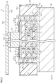
FIG. 2 is a sectional view illustrating the sectional structure of an electronic control device according to a first embodiment; and -
FIG. 3 is a sectional view illustrating the sectional structure of an electronic control device according to a second embodiment. - An electronic control device according to a first embodiment of the present invention is described below.
- As illustrated in
FIG. 1 , anelectronic control device 1 is used for controlling operation of, for example, a motor of an electric power steering system to be mounted on a vehicle. Theelectronic control device 1 includes aheating element 10, a rectangular plate-like circuit substrate 20, and a rectangular plate-likeheat radiation plate 30 serving as a first heat radiator, which is indicated by an imaginary line. - The
heating element 10 has a plurality ofconnection terminals 13. Examples of theheating element 10 include an integrated circuit (IC) and a field effect transistor (FET). Theconnection terminal 13 is fixed to thecircuit substrate 20 withsolder 14. Thesolder 14 covers theentire connection terminal 13. Theheat radiation plate 30 is formed of a metal material having a high thermal conductivity, such as an aluminum alloy. - As illustrated in
FIG. 2 , thecircuit substrate 20 has acircuit principal surface 20a as one surface, and a circuit principal surface 20b as the other surface. In theelectronic control device 1, theheat radiation plate 30 is provided so as to face thecircuit principal surface 20b of thecircuit substrate 20, and theheating element 10 is provided on thecircuit principal surface 20a of thecircuit substrate 20. Thecircuit substrate 20 has a predetermined thickness T1. Thecircuit substrate 20 has a multilayer structure in which first to fourth circuit conductor layers 20c to 20f are laminated with first to third insulatinglayers 20g to 20i respectively interposed therebetween. Specifically, thecircuit substrate 20 is formed by laminating the firstcircuit conductor layer 20c, the first insulatinglayer 20g, the secondcircuit conductor layer 20d, the second insulatinglayer 20h, the thirdcircuit conductor layer 20e, the third insulating layer 20i, and the fourthcircuit conductor layer 20f in the order from theheating element 10 side. Each of the first to fourth circuit conductor layers 20c to 20f haswiring patterns 21 serving as substrate electrodes, which are formed by removing a part of conductive foil such as copper foil by etching or the like. A clearance between thewiring patterns 21 formed in each of the second and third circuit conductor layers 20d and 20e is filled with an insulating resin material. Each of the first to third insulatinglayers 20g to 20i is formed of an insulating resin material to maintain insulation between thewiring patterns 21 adjacent to each other in a direction orthogonal to thecircuit substrate 20. Thecircuit substrate 20 has a plurality of via holes (interlayer connection holes) 20j passing through predetermined circuit conductor layers and insulating layers and extending in a laminating direction (vertical direction inFIG. 2 ). Aconnection member 20k formed of a conductive material such as copper is inserted into the viahole 20j. Thewiring patterns 21 of different layers are electrically connected to each other via theconnection member 20k. Thecircuit substrate 20 has a plurality of cylindrical through holes 22. The throughhole 22 passes through thecircuit substrate 20 in its thickness direction. The throughhole 22 is open to each of the circuitprincipal surface 20a and the circuitprincipal surface 20b. The throughhole 22 has its inner peripheral surface coated withconductive plating 22a such as copper foil. Theconductive plating 22a provided on the inner peripheral surface of the throughhole 22 is in contact withpredetermined wiring patterns 21 of the first to fourth circuit conductor layers 20c to 20f. - As illustrated in
FIG. 1 , thecircuit substrate 20 has eight throughholes 22. The through holes 22 are arranged away from the distal ends of theconnection terminals 13 of the heating element 10 (peripheral edges of the heating element 10) by a distance T2 equal to or smaller than the substrate thickness T1. The through holes 22 are arranged with intervals over the entire periphery of theheating element 10. Specifically, two throughholes 22 are arranged on each side of theheating element 10 correspondingly. - As illustrated in
FIG. 2 , aheat radiation material 40 is applied between the circuitprincipal surface 20b of thecircuit substrate 20 and theheat radiation plate 30. Further, theheat radiation material 40 is filled in the through holes 22. Theheat radiation material 40 filled in the throughholes 22 is exposed to the circuitprincipal surface 20a of thecircuit substrate 20. Theheat radiation material 40 is heat radiation grease having an insulating property and a curability. For example, theheat radiation material 40 is gradually cured by absorbing moisture in the air. Theheat radiation material 40 described above is an example and may be changed as appropriate depending on product specifications. - As illustrated in
FIG. 1 , theheat radiation material 40 exposed to the circuitprincipal surface 20a covers the distal ends of a plurality ofarbitrary connection terminals 13 located in the vicinity of the throughhole 22 among theconnection terminals 13 of theheating element 10 that are fixed with thesolder 14. Specifically, theheat radiation material 40 is applied so as to further cover thesolder 14 that covers theconnection terminals 13. - Next, a method for assembling the
electronic control device 1 is described. - First, the
connection terminals 13 of theheating element 10 are fixed to thewiring patterns 21 on the circuitprincipal surface 20a of thecircuit substrate 20 with thesolder 14. Next, a predetermined amount of theheat radiation material 40 is applied to the surface of theheat radiation plate 30. Then, the circuitprincipal surface 20b of thecircuit substrate 20 and the surface of theheat radiation plate 30 where theheat radiation material 40 is applied are caused to face each other. The circuitprincipal surface 20b and the surface of theheat radiation plate 30 where theheat radiation material 40 is applied are brought closer to each other. Theheat radiation material 40 receives pressing forces in an assembling direction from both of thecircuit substrate 20 and theheat radiation plate 30 to spread all over the circuitprincipal surface 20b and the surface of theheat radiation plate 30. Theheat radiation material 40 enters and fills the throughholes 22 provided in thecircuit substrate 20 by the pressing forces received from both of thecircuit substrate 20 and theheat radiation plate 30. When theheat radiation material 40 is filled in the throughholes 22 and is exposed to the circuitprincipal surface 20a of thecircuit substrate 20, the circuitprincipal surface 20b and the surface of theheat radiation plate 30 where theheat radiation material 40 is applied are no longer brought closer to each other. Lastly, the uncuredheat radiation material 40 exposed to the circuitprincipal surface 20a is applied so as to further cover thesolder 14 that covers theconnection terminals 13. When theheat radiation material 40 is sufficiently cured by absorbing moisture in the air, the assembling of theelectronic control device 1 is completed. - As described above in detail, the
electronic control device 1 according to this embodiment attains the following actions and effects. - (1) The cylindrical through
holes 22 passing through thecircuit substrate 20 in its thickness direction are provided in thecircuit substrate 20 at positions spaced away from the distal ends of theconnection terminals 13 of the heating element 10 (peripheral edges of the heating element 10). Therefore, the condition of theheat radiation material 40 applied between the circuitprincipal surface 20b of thecircuit substrate 20 and theheat radiation plate 30 can be checked via the through holes 22. - (2) The
conductive plating 22a provided on the inner peripheral surface of the throughhole 22 is in contact witharbitrary wiring patterns 21 of the first to fourth circuit conductor layers 20c to 20f of thecircuit substrate 20. Therefore, heat generated from theheating element 10 is transferred to theconnection terminals 13, and is further transferred from theconnection terminals 13 to theheat radiation material 40 filled in the throughhole 22 via thewiring patterns 21 of thecircuit substrate 20. Thus, the heat radiation effect for the heat generated from theheating element 10 can further be improved. - (3) The
heat radiation material 40 is exposed to the circuitprincipal surface 20a of thecircuit substrate 20 via the through holes 22. The exposure of theheat radiation material 40 to the circuitprincipal surface 20a of thecircuit substrate 20 via the throughholes 22 indicates that theheat radiation material 40 is sufficiently applied between thecircuit substrate 20 and theheat radiation plate 30. Therefore, it is only necessary to check that theheat radiation material 40 is exposed to the circuitprincipal surface 20a. Thus, it is possible to check more easily that theheat radiation material 40 is appropriately applied between the circuitprincipal surface 20b of thecircuit substrate 20 and theheat radiation plate 30. - (4) At least a part of the
connection terminals 13 of theheating element 10 is covered with theheat radiation material 40 exposed to the circuitprincipal surface 20a of thecircuit substrate 20. Therefore, the heat generated from theheating element 10 is directly transferred to theheat radiation material 40. Thus, the heat radiation effect for the heat generated from theheating element 10 can further be improved. - (5) The
heat radiation material 40 is the heat radiation grease having the curability and the insulating property. Theconnection terminals 13 of theheating element 10 that are connected to thewiring patterns 21 with thesolder 14 are covered with theheat radiation material 40 that has the curability and is exposed to the circuitprincipal surface 20a of thecircuit substrate 20. Therefore, the maintainability of connection of theconnection terminals 13 of theheating element 10 to thewiring patterns 21 can be improved. Theheat radiation material 40 has the insulating property, and therefore the insulation between theadjacent connection terminals 13 can also be improved in a state in which theconnection terminals 13 and thewiring patterns 21 are connected to each other. - (6) In general, it is known that heat is radially transferred from a heat source. Therefore, the through
holes 22 are provided in thecircuit substrate 20 along the entire periphery of theheating element 10. Thus, the heat generated from theheating element 10 can be radiated more effectively. - (7) The through
holes 22 are provided away from the distal ends of theconnection terminals 13 of theheating element 10 by the distance T2 equal to or smaller than the substrate thickness T1. Therefore, a path along which the heat generated from theheating element 10 is transferred from the circuitprincipal surface 20a of thecircuit substrate 20 to theheat radiation plate 30 via theheat radiation material 40 filled in the throughholes 22 can be used as a heat transfer path in addition to a path along which the heat generated from theheating element 10 is transferred from the circuitprincipal surface 20a of thecircuit substrate 20 to the circuitprincipal surface 20b of thecircuit substrate 20 and is further transferred to theheat radiation plate 30 via theheat radiation material 40. That is, the heat radiation effect for theheating element 10 can be improved. - An electronic control device according to a second embodiment is described below. The electronic control device of this embodiment is different from the electronic control device of the first embodiment in that a heat radiation plate other than the
heat radiation plate 30 is provided. Therefore, components similar to those of the first embodiment are represented by the same reference symbols to omit detailed description of the components. - As illustrated in
FIG. 3 , aheat radiation plate 50 serving as a first heat radiator is provided on a surface of theheating element 10 that is opposite to thecircuit substrate 20. Theheat radiation plate 50 is provided through intermediation of aheat radiation material 45 serving as a second heat radiator. - The
heat radiation plate 50 hasprincipal surfaces 50a and 50b. The principal surface 50a is a surface of theheat radiation plate 50 that is opposite to thecircuit substrate 20, and theprincipal surface 50b is a surface of theheat radiation plate 50 that faces thecircuit substrate 20. Theheat radiation plate 50 employed herein has a rectangular shape and has a slightly larger size than that of theheat radiation plate 30. Theheat radiation plate 50 is provided so as to cover theheating element 10. A part of theheat radiation plate 50 other than the part where theheating element 10 is provided faces thecircuit substrate 20 with a clearance therebetween. The shape of theheat radiation plate 50 is not limited to the rectangular shape, and may be changed as appropriate as long as theheat radiation plate 50 has a shape and size capable of covering theheating element 10. - The
heat radiation plate 50 has a plurality of cylindrical through holes 51. The through holes 51 are provided within a range of a part of theheat radiation plate 50 that faces a surface 10a of theheating element 10 that is opposite to thecircuit substrate 20. The throughhole 51 passes through theheat radiation plate 50 in its thickness direction. The throughhole 51 is open to each of the principal surface 50a and theprincipal surface 50b of theheat radiation plate 50. - The
heat radiation material 45 is applied between the surface 10a of theheating element 10 and theheat radiation plate 50. Further, theheat radiation material 45 is filled in the through holes 51. Theheat radiation material 45 filled in the throughholes 51 is exposed to the principal surface 50a of theheat radiation plate 50. Theheat radiation material 45 is the same as theheat radiation material 40 interposed between the circuitprincipal surface 20b of thecircuit substrate 20 and theheat radiation plate 30. - Next, a method for assembling the
electronic control device 1 is described. Theheating element 10, thecircuit substrate 20, and theheat radiation plate 30 are assembled similarly to the first embodiment. - After the
heating element 10, thecircuit substrate 20, and theheat radiation plate 30 are assembled and the condition of the appliedheat radiation material 40 is checked, a predetermined amount of theheat radiation material 45 is applied to the surface 10a of theheating element 10. Then, the surface 10a of theheating element 10 and theprincipal surface 50b of theheat radiation plate 50 are brought closer to each other in a state in which the surface 10a and theprincipal surface 50b are caused to face each other. Theheat radiation material 45 receives pressing forces in an assembling direction from both of theheating element 10 and theheat radiation plate 50 to spread all over the space between the surface 10a and a part of theprincipal surface 50b that faces the surface 10a. Theheat radiation material 45 enters and fills the throughholes 51 of theheat radiation plate 50 by the pressing forces received from both of theheating element 10 and theheat radiation plate 50. When theheat radiation material 45 is filled in the throughholes 51 and is exposed to the principal surface 50a of theheat radiation plate 50, the surface 10a and theprincipal surface 50b are no longer brought closer to each other. Lastly, when theheat radiation material 45 is sufficiently cured by absorbing moisture in the air, the assembling of theelectronic control device 1 is completed. - According to this embodiment, the following effects are attained in addition to the effects (1) to (6) of the first embodiment. That is, the condition of the
heat radiation material 45 interposed between the surface 10a of theheating element 10 and theprincipal surface 50b of theheat radiation plate 50 can be checked via the through holes 51. Further, theheat radiation material 45 has a curability. Therefore, the adhesion between theheating element 10 and theheat radiation plate 50 is improved such that theheat radiation material 45 enters the throughholes 51 and is cured (anchor effect). - The first embodiment and the second embodiment may be modified as follows without technical contradiction.
- In the first and second embodiments, the
heat radiation materials principal surface 20a of thecircuit substrate 20 and the principal surface 50a of theheat radiation plate 50 via the throughholes heat radiation materials principal surface 20a and the principal surface 50a, respectively. For example, theheat radiation materials holes heat radiation material 40 is appropriately applied between thecircuit substrate 20 and theheat radiation plate 30 and that theheat radiation material 45 is appropriately applied between theheating element 10 and theheat radiation plate 50 based on the conditions that theheat radiation materials holes - In the first and second embodiments, the
circuit substrate 20 has eight throughholes 22, but the present invention is not limited thereto. For example, the number of throughholes 22 may be set to more than eight. With this setting, the heat radiation effect for the heat generated from theheating element 10 can be improved. Further, the number of throughholes 22 may be set to less than eight. In this case, it is effective to provide the throughholes 22 at positions corresponding to at least the respective sides of theheating element 10. However, the positions of the throughholes 22 may be changed as appropriate depending on product specifications. For example, the throughholes 22 may be provided at positions corresponding to a part of the sides of theheating element 10 instead of all the sides. - In the second embodiment, the
heat radiation plate 50 has the plurality of throughholes 51, but may only have one throughhole 51. Also in this case, the condition of theheat radiation material 45 interposed between theheating element 10 and theheat radiation plate 50 can be checked. - In the first and second embodiments, the through
holes 22 are provided away from the peripheral edges of theheating element 10 by the distance T2 equal to or smaller than the thickness T1 of thecircuit substrate 20, but the present invention is not limited thereto. For example, the throughholes 22 may be provided away from the peripheral edges of theheating element 10 by a distance larger than the thickness T1 of thecircuit substrate 20. In this case, the throughholes 22 are provided within a range in which theheat radiation material 40 is applied between the circuitprincipal surface 20b of thecircuit substrate 20 and theheat radiation plate 30. - In the first and second embodiments, the through
hole 22 is in contact with thewiring patterns 21 via theconductive plating 22a, but the present invention is not limited thereto. For example, theconductive plating 22a may be omitted. In this case, it is only necessary that theheat radiation material 40 filled in the throughhole 22 and thewiring patterns 21 be in contact with each other. As another example, thewiring patterns 21 may pass through theconductive plating 22a. - In the first and second embodiments, the
heat radiation material 40 exposed to the circuitprincipal surface 20a is applied so as to cover the distal ends ofarbitrary connection terminals 13 among theconnection terminals 13 of theheating element 10 that are fixed with thesolder 14, but the present invention is not limited thereto. For example, theheat radiation material 40 may be applied so as to cover the distal ends of all theconnection terminals 13. - In the first and second embodiments, the
heat radiation material 40 is applied so as to cover thesolder 14, but the present invention is not limited thereto. For example, theheat radiation material 40 may be applied so as to fill a clearance between the adjacent connection terminals 13 (pieces of solder 14). Also in this case, the insulation between theadjacent connection terminals 13 can be secured and the maintainability of connection of theconnection terminals 13 to thewiring patterns 21 can be improved. At least the maintainability of connection of theconnection terminals 13 to thewiring patterns 21 can be improved by applying theheat radiation material 40 so as to cover at least a part of theconnection terminals 13. - In the first and second embodiments, the
heat radiation materials heat radiation materials heat radiation materials heat radiation materials heat radiation materials connection terminals 13 to thewiring patterns 21 can be improved by covering a part of theconnection terminals 13 with theheat radiation material 40. In the second embodiment, the adhesion between theheating element 10 and theheat radiation plate 50 can be improved by the anchor effect. - In the first and second embodiments, the
circuit substrate 20 has the multilayer structure in which the first to fourth circuit conductor layers 20c to 20f are laminated with the first to third insulatinglayers 20g to 20i respectively interposed therebetween, but the present invention is not limited thereto. For example, thecircuit substrate 20 may have a single-layer structure. - In the first and second embodiments, the
heat radiation plate 30 is in contact with thecircuit substrate 20 via theheat radiation material 40, but the present invention is not limited thereto. For example, the size of theheat radiation plate 30 may be set substantially equal to the size of thecircuit substrate 20 and theheat radiation plate 30 and thecircuit substrate 20 may be in contact with each other on their peripheral edges. In this case, thecircuit substrate 20 and theheat radiation plate 30 may be fixed to each other with bolts or the like at their contact positions. - In the first and second embodiments, the
heat radiation materials heat radiation materials heat radiation materials circuit substrate 20 and theheat radiation plate 30 be fixed to each other with bolts or the like and that thecircuit substrate 20 and theheat radiation plate 50 be fixed to each other with bolts or the like. As another example, theheat radiation materials heat radiation materials heating element 10 where the insulating property is not required. - In the second embodiment, the
heat radiation material 40 is interposed between thecircuit substrate 20 and theheat radiation plate 30 and theheat radiation material 45 is applied between theheating element 10 and theheat radiation plate 50, but the present invention is not limited thereto. For example, theheat radiation material 40 need not be interposed between thecircuit substrate 20 and theheat radiation plate 30. In this case, only theheat radiation material 45 may be applied between theheating element 10 and theheat radiation plate 50 while theheat radiation plate 30 is omitted. - The
heat radiation plates heat radiation materials heat radiation plate 30 and thecircuit substrate 20 and between theheat radiation plate 50 and theheating element 10, respectively. In this case, it is appropriate that the conditions of theheat radiation materials holes - An electronic control device (1) includes a heating element (10), a circuit substrate (20), a heat radiation plate (30), and a heat radiation material (40). Connection terminals (13) of the heating element (10) are fixed to wiring patterns (21) on a circuit principal surface (20a) of the circuit substrate (20) with solder (14). Through holes (22) are provided in the circuit substrate (20) at portions spaced away from the distal ends of the connection terminals (13) of the heating element (10) by a distance (T2) equal to or smaller than a thickness (T1) of the circuit substrate (20). The heat radiation material (40) applied between a circuit principal surface (20b) of the circuit substrate (20) and the heat radiation plate (30) is exposed to the circuit principal surface (20a) via the through holes (22). The heat radiation material (40) exposed to the circuit principal surface (20a) covers the distal ends of the connection terminals (13) fixed with the solder (14). When a heat radiation material is interposed between the heating element (10) and a heat radiation plate, the condition of the heat radiation material can be checked by providing through holes in the heat radiation plate.
Claims (6)
- An electronic control device, comprising:a substrate provided with a heating element on one surface;a second heat radiator provided on at least one of the other surface of the substrate that is opposite to the one surface of the substrate and a surface of the heating element that is opposite to the substrate; anda first heat radiator provided such that the second heat radiator is interposed between the first heat radiator and at least one of the other surface of the substrate and the surface of the heating element that is opposite to the substrate, whereinwhen the second heat radiator is provided on the other surface of the substrate, the substrate has a through hole that passes through the substrate in its thickness direction and is provided away from peripheral edges of the heating element at a position where the second heat radiator is interposed, andwhen the second heat radiator is provided on the surface of the heating element that is opposite to the substrate, the first heat radiator provided such that the second heat radiator is interposed between the first heat radiator and the heating element has a through hole that passes through the first heat radiator in its thickness direction and is provided within a range of a part of the first heat radiator that corresponds to the heating element.
- The electronic control device according to claim 1, wherein
the heating element has a plurality of terminals on its peripheral edges,
the substrate has substrate electrodes,
the terminals are connected to the substrate electrodes with solder, and
a part of the substrate electrodes is exposed to an inside of the through hole of the substrate. - The electronic control device according to claim 1 or 2, wherein
when the second heat radiator is provided on the other surface of the substrate, the second heat radiator is exposed to the one surface of the substrate via the through hole provided in the substrate. - The electronic control device according to claim 3, wherein
the heating element has a plurality of terminals on its peripheral edges,
the terminals are connected, with solder, to substrate electrodes provided on the one surface of the substrate, and
at least a part of the terminals is covered with the second heat radiator exposed to the one surface of the substrate. - The electronic control device according to claim 4, wherein
the second heat radiator has a curability and an insulating property. - The electronic control device according to any one of claims 1 to 5, wherein
when the second heat radiator is provided on the surface of the heating element that is opposite to the substrate, the second heat radiator provided on the surface of the heating element that is opposite to the substrate is exposed to an outside via the through hole of the first heat radiator provided such that the second heat radiator is interposed between the first heat radiator and the heating element.
Applications Claiming Priority (2)
| Application Number | Priority Date | Filing Date | Title |
|---|---|---|---|
| JP2016179843 | 2016-09-14 | ||
| JP2016186121A JP6878806B2 (en) | 2016-09-14 | 2016-09-23 | Electronic control device |
Publications (2)
| Publication Number | Publication Date |
|---|---|
| EP3297021A1 true EP3297021A1 (en) | 2018-03-21 |
| EP3297021B1 EP3297021B1 (en) | 2022-04-13 |
Family
ID=59914284
Family Applications (1)
| Application Number | Title | Priority Date | Filing Date |
|---|---|---|---|
| EP17190518.5A Not-in-force EP3297021B1 (en) | 2016-09-14 | 2017-09-12 | Electronic control device |
Country Status (3)
| Country | Link |
|---|---|
| US (1) | US10420255B2 (en) |
| EP (1) | EP3297021B1 (en) |
| CN (1) | CN107820376A (en) |
Families Citing this family (1)
| Publication number | Priority date | Publication date | Assignee | Title |
|---|---|---|---|---|
| TWI790671B (en) * | 2021-07-04 | 2023-01-21 | 郭明騰 | Light source module |
Citations (11)
| Publication number | Priority date | Publication date | Assignee | Title |
|---|---|---|---|---|
| DE2741320A1 (en) * | 1977-09-14 | 1979-03-22 | Blaupunkt Werke Gmbh | Semiconductor component mounted on support - has heat sink over component and support part, with filling substance of high heat conductivity in between |
| EP0600590A1 (en) * | 1992-12-03 | 1994-06-08 | International Computers Limited | Cooling electronic circuit assemblies |
| US6188578B1 (en) * | 1999-06-11 | 2001-02-13 | Industrial Technology Research Institute | Integrated circuit package with multiple heat dissipation paths |
| US20040233642A1 (en) * | 2003-05-19 | 2004-11-25 | Kazutoshi Ito | Heat dissipation structure |
| US20050063162A1 (en) * | 2002-12-23 | 2005-03-24 | Eastman Kodak Company | Electrical assemblage and method for removing heat locally generated therefrom |
| JP2006054481A (en) * | 2005-09-22 | 2006-02-23 | Denso Corp | Electronic control device |
| JP2011165903A (en) * | 2010-02-10 | 2011-08-25 | Rohm Co Ltd | Semiconductor module and method of manufacturing the same |
| JP2014135418A (en) | 2013-01-11 | 2014-07-24 | Hitachi Automotive Systems Ltd | On-vehicle electronic control device |
| EP2884530A2 (en) * | 2013-12-13 | 2015-06-17 | Huawei Technologies Co., Ltd. | Heat sink and heat dissipation system |
| JP2015135852A (en) | 2014-01-16 | 2015-07-27 | 株式会社東芝 | semiconductor device |
| US9253925B1 (en) * | 2013-01-11 | 2016-02-02 | L-3 Communications Corp. | Panel for enhancing thermal conduction in an electronic assembly |
Family Cites Families (15)
| Publication number | Priority date | Publication date | Assignee | Title |
|---|---|---|---|---|
| US5258887A (en) * | 1992-06-15 | 1993-11-02 | Eaton Corporation | Electrical device cooling system using a heat sink attached to a circuit board containing heat conductive layers and channels |
| WO1994018701A1 (en) * | 1993-02-05 | 1994-08-18 | W.L. Gore & Associates, Inc. | Stress-resistant semiconductor chip-circuit board interconnect |
| US5586008A (en) * | 1994-09-06 | 1996-12-17 | Methode Electronics, Inc. | Gravity latch for surface mount components |
| SG48462A1 (en) * | 1995-10-26 | 1998-04-17 | Ibm | Lead protective coating composition process and structure thereof |
| JP3830726B2 (en) * | 2000-04-26 | 2006-10-11 | 松下電器産業株式会社 | Thermally conductive substrate, manufacturing method thereof, and power module |
| JP4923336B2 (en) * | 2001-04-10 | 2012-04-25 | 日本電気株式会社 | Circuit board and electronic device using the circuit board |
| JP2004172459A (en) * | 2002-11-21 | 2004-06-17 | Advics:Kk | Heat dissipation structure of electronic components in electronic control unit |
| JP3804803B2 (en) * | 2004-02-12 | 2006-08-02 | 沖電気工業株式会社 | Electronic component mounting substrate and semiconductor device |
| WO2005093827A1 (en) * | 2004-03-26 | 2005-10-06 | Fujikura Ltd. | Through wiring board and method for producing the same |
| JP2009206506A (en) * | 2008-01-31 | 2009-09-10 | Sanyo Electric Co Ltd | Substrate for mounting element and its manufacturing method, semiconductor module and portable device mounted with the same |
| JP2010103244A (en) * | 2008-10-22 | 2010-05-06 | Sony Corp | Semiconductor device, and method of manufacturing the same |
| JP5121783B2 (en) * | 2009-06-30 | 2013-01-16 | 株式会社日立ハイテクノロジーズ | LED light source, manufacturing method thereof, exposure apparatus using LED light source, and exposure method |
| JP2014127522A (en) * | 2012-12-25 | 2014-07-07 | Keihin Corp | Heat radiation structure of printed circuit board |
| ITMI20130520A1 (en) * | 2013-04-05 | 2014-10-06 | St Microelectronics Srl | CONSTRUCTION OF A HEAT SINK THROUGH WELDING |
| JP6771308B2 (en) * | 2016-05-02 | 2020-10-21 | 三菱電機株式会社 | Mounting structure of circuit boards and semiconductor integrated circuits |
-
2017
- 2017-09-11 US US15/700,522 patent/US10420255B2/en active Active
- 2017-09-12 EP EP17190518.5A patent/EP3297021B1/en not_active Not-in-force
- 2017-09-13 CN CN201710821290.XA patent/CN107820376A/en active Pending
Patent Citations (11)
| Publication number | Priority date | Publication date | Assignee | Title |
|---|---|---|---|---|
| DE2741320A1 (en) * | 1977-09-14 | 1979-03-22 | Blaupunkt Werke Gmbh | Semiconductor component mounted on support - has heat sink over component and support part, with filling substance of high heat conductivity in between |
| EP0600590A1 (en) * | 1992-12-03 | 1994-06-08 | International Computers Limited | Cooling electronic circuit assemblies |
| US6188578B1 (en) * | 1999-06-11 | 2001-02-13 | Industrial Technology Research Institute | Integrated circuit package with multiple heat dissipation paths |
| US20050063162A1 (en) * | 2002-12-23 | 2005-03-24 | Eastman Kodak Company | Electrical assemblage and method for removing heat locally generated therefrom |
| US20040233642A1 (en) * | 2003-05-19 | 2004-11-25 | Kazutoshi Ito | Heat dissipation structure |
| JP2006054481A (en) * | 2005-09-22 | 2006-02-23 | Denso Corp | Electronic control device |
| JP2011165903A (en) * | 2010-02-10 | 2011-08-25 | Rohm Co Ltd | Semiconductor module and method of manufacturing the same |
| JP2014135418A (en) | 2013-01-11 | 2014-07-24 | Hitachi Automotive Systems Ltd | On-vehicle electronic control device |
| US9253925B1 (en) * | 2013-01-11 | 2016-02-02 | L-3 Communications Corp. | Panel for enhancing thermal conduction in an electronic assembly |
| EP2884530A2 (en) * | 2013-12-13 | 2015-06-17 | Huawei Technologies Co., Ltd. | Heat sink and heat dissipation system |
| JP2015135852A (en) | 2014-01-16 | 2015-07-27 | 株式会社東芝 | semiconductor device |
Also Published As
| Publication number | Publication date |
|---|---|
| EP3297021B1 (en) | 2022-04-13 |
| US10420255B2 (en) | 2019-09-17 |
| CN107820376A (en) | 2018-03-20 |
| US20180077825A1 (en) | 2018-03-15 |
Similar Documents
| Publication | Publication Date | Title |
|---|---|---|
| US9253888B2 (en) | Method for integrating an electronic component into a printed circuit board or a printed circuit board intermediate product, and printed circuit board or printed circuit board intermediate product | |
| US6995476B2 (en) | Semiconductor device, circuit board and electronic instrument that include an adhesive with conductive particles therein | |
| CN106463930A (en) | Circuit structure and electric junction box | |
| CN102210199B (en) | electronic circuit device | |
| US20090008771A1 (en) | Semiconductor module device, method of manufacturing the same, flat panel display, and plasma display panel | |
| US10398020B2 (en) | Circuit assembly and manufacturing method of circuit assembly | |
| KR20000068821A (en) | Assembly Consisting of a Substrate for Power Components and a Cooling Element and Method for the Production Thereof | |
| JP6477373B2 (en) | Circuit assembly and electrical junction box | |
| CN101237746A (en) | Electronic board with heating resistors | |
| CN105551977A (en) | Method for producing a switching device with a moisture-tight and electrically insulating cover and for producing an arrangement therewith | |
| US10820406B2 (en) | Circuit structure and electrical junction box | |
| JP2021174847A (en) | Electronics | |
| CN107006126A (en) | Utilize the electronic apparatus module particularly for automotive drive control device of face contact sandwich building block technique | |
| EP3297021B1 (en) | Electronic control device | |
| US20190373740A1 (en) | Method for manufacturing printed wiring board | |
| US9924590B2 (en) | Printed board and electronic apparatus | |
| JP6878806B2 (en) | Electronic control device | |
| JP6488658B2 (en) | Electronic equipment | |
| EP3823424A1 (en) | Connection structure including circuit body and conductive body | |
| US20250247943A1 (en) | Circuit board structure and electric compressor including the same | |
| JPWO2017119087A1 (en) | Electronic device and electronic module | |
| CN121079875A (en) | Electronic control device | |
| CN117939773A (en) | Printed circuit board and heat dissipation method thereof | |
| CN121510448A (en) | Manufacturing processes of electrical control components, outdoor air conditioning units, air conditioners, and electrical control components | |
| WO2018221296A1 (en) | Power conversion device |
Legal Events
| Date | Code | Title | Description |
|---|---|---|---|
| PUAI | Public reference made under article 153(3) epc to a published international application that has entered the european phase |
Free format text: ORIGINAL CODE: 0009012 |
|
| STAA | Information on the status of an ep patent application or granted ep patent |
Free format text: STATUS: THE APPLICATION HAS BEEN PUBLISHED |
|
| AK | Designated contracting states |
Kind code of ref document: A1 Designated state(s): AL AT BE BG CH CY CZ DE DK EE ES FI FR GB GR HR HU IE IS IT LI LT LU LV MC MK MT NL NO PL PT RO RS SE SI SK SM TR |
|
| AX | Request for extension of the european patent |
Extension state: BA ME |
|
| STAA | Information on the status of an ep patent application or granted ep patent |
Free format text: STATUS: REQUEST FOR EXAMINATION WAS MADE |
|
| 17P | Request for examination filed |
Effective date: 20180717 |
|
| STAA | Information on the status of an ep patent application or granted ep patent |
Free format text: STATUS: EXAMINATION IS IN PROGRESS |
|
| 17Q | First examination report despatched |
Effective date: 20210126 |
|
| REG | Reference to a national code |
Ref country code: DE Ref legal event code: R079 Ref document number: 602017055823 Country of ref document: DE Free format text: PREVIOUS MAIN CLASS: H01L0023367000 Ipc: H05K0003000000 |
|
| GRAP | Despatch of communication of intention to grant a patent |
Free format text: ORIGINAL CODE: EPIDOSNIGR1 |
|
| STAA | Information on the status of an ep patent application or granted ep patent |
Free format text: STATUS: GRANT OF PATENT IS INTENDED |
|
| RIC1 | Information provided on ipc code assigned before grant |
Ipc: H05K 1/11 20060101ALI20211007BHEP Ipc: H05K 1/02 20060101ALI20211007BHEP Ipc: H01L 23/42 20060101ALI20211007BHEP Ipc: H01L 23/367 20060101ALI20211007BHEP Ipc: H05K 3/00 20060101AFI20211007BHEP |
|
| INTG | Intention to grant announced |
Effective date: 20211028 |
|
| GRAS | Grant fee paid |
Free format text: ORIGINAL CODE: EPIDOSNIGR3 |
|
| GRAA | (expected) grant |
Free format text: ORIGINAL CODE: 0009210 |
|
| STAA | Information on the status of an ep patent application or granted ep patent |
Free format text: STATUS: THE PATENT HAS BEEN GRANTED |
|
| RAP3 | Party data changed (applicant data changed or rights of an application transferred) |
Owner name: JTEKT CORPORATION |
|
| AK | Designated contracting states |
Kind code of ref document: B1 Designated state(s): AL AT BE BG CH CY CZ DE DK EE ES FI FR GB GR HR HU IE IS IT LI LT LU LV MC MK MT NL NO PL PT RO RS SE SI SK SM TR |
|
| REG | Reference to a national code |
Ref country code: GB Ref legal event code: FG4D |
|
| REG | Reference to a national code |
Ref country code: CH Ref legal event code: EP |
|
| REG | Reference to a national code |
Ref country code: DE Ref legal event code: R096 Ref document number: 602017055823 Country of ref document: DE |
|
| REG | Reference to a national code |
Ref country code: IE Ref legal event code: FG4D |
|
| REG | Reference to a national code |
Ref country code: AT Ref legal event code: REF Ref document number: 1484427 Country of ref document: AT Kind code of ref document: T Effective date: 20220515 |
|
| REG | Reference to a national code |
Ref country code: LT Ref legal event code: MG9D |
|
| REG | Reference to a national code |
Ref country code: NL Ref legal event code: MP Effective date: 20220413 |
|
| REG | Reference to a national code |
Ref country code: AT Ref legal event code: MK05 Ref document number: 1484427 Country of ref document: AT Kind code of ref document: T Effective date: 20220413 |
|
| PG25 | Lapsed in a contracting state [announced via postgrant information from national office to epo] |
Ref country code: NL Free format text: LAPSE BECAUSE OF FAILURE TO SUBMIT A TRANSLATION OF THE DESCRIPTION OR TO PAY THE FEE WITHIN THE PRESCRIBED TIME-LIMIT Effective date: 20220413 |
|
| PG25 | Lapsed in a contracting state [announced via postgrant information from national office to epo] |
Ref country code: SE Free format text: LAPSE BECAUSE OF FAILURE TO SUBMIT A TRANSLATION OF THE DESCRIPTION OR TO PAY THE FEE WITHIN THE PRESCRIBED TIME-LIMIT Effective date: 20220413 Ref country code: PT Free format text: LAPSE BECAUSE OF FAILURE TO SUBMIT A TRANSLATION OF THE DESCRIPTION OR TO PAY THE FEE WITHIN THE PRESCRIBED TIME-LIMIT Effective date: 20220816 Ref country code: NO Free format text: LAPSE BECAUSE OF FAILURE TO SUBMIT A TRANSLATION OF THE DESCRIPTION OR TO PAY THE FEE WITHIN THE PRESCRIBED TIME-LIMIT Effective date: 20220713 Ref country code: LT Free format text: LAPSE BECAUSE OF FAILURE TO SUBMIT A TRANSLATION OF THE DESCRIPTION OR TO PAY THE FEE WITHIN THE PRESCRIBED TIME-LIMIT Effective date: 20220413 Ref country code: HR Free format text: LAPSE BECAUSE OF FAILURE TO SUBMIT A TRANSLATION OF THE DESCRIPTION OR TO PAY THE FEE WITHIN THE PRESCRIBED TIME-LIMIT Effective date: 20220413 Ref country code: GR Free format text: LAPSE BECAUSE OF FAILURE TO SUBMIT A TRANSLATION OF THE DESCRIPTION OR TO PAY THE FEE WITHIN THE PRESCRIBED TIME-LIMIT Effective date: 20220714 Ref country code: FI Free format text: LAPSE BECAUSE OF FAILURE TO SUBMIT A TRANSLATION OF THE DESCRIPTION OR TO PAY THE FEE WITHIN THE PRESCRIBED TIME-LIMIT Effective date: 20220413 Ref country code: ES Free format text: LAPSE BECAUSE OF FAILURE TO SUBMIT A TRANSLATION OF THE DESCRIPTION OR TO PAY THE FEE WITHIN THE PRESCRIBED TIME-LIMIT Effective date: 20220413 Ref country code: BG Free format text: LAPSE BECAUSE OF FAILURE TO SUBMIT A TRANSLATION OF THE DESCRIPTION OR TO PAY THE FEE WITHIN THE PRESCRIBED TIME-LIMIT Effective date: 20220713 Ref country code: AT Free format text: LAPSE BECAUSE OF FAILURE TO SUBMIT A TRANSLATION OF THE DESCRIPTION OR TO PAY THE FEE WITHIN THE PRESCRIBED TIME-LIMIT Effective date: 20220413 |
|
| PG25 | Lapsed in a contracting state [announced via postgrant information from national office to epo] |
Ref country code: RS Free format text: LAPSE BECAUSE OF FAILURE TO SUBMIT A TRANSLATION OF THE DESCRIPTION OR TO PAY THE FEE WITHIN THE PRESCRIBED TIME-LIMIT Effective date: 20220413 Ref country code: PL Free format text: LAPSE BECAUSE OF FAILURE TO SUBMIT A TRANSLATION OF THE DESCRIPTION OR TO PAY THE FEE WITHIN THE PRESCRIBED TIME-LIMIT Effective date: 20220413 Ref country code: LV Free format text: LAPSE BECAUSE OF FAILURE TO SUBMIT A TRANSLATION OF THE DESCRIPTION OR TO PAY THE FEE WITHIN THE PRESCRIBED TIME-LIMIT Effective date: 20220413 Ref country code: IS Free format text: LAPSE BECAUSE OF FAILURE TO SUBMIT A TRANSLATION OF THE DESCRIPTION OR TO PAY THE FEE WITHIN THE PRESCRIBED TIME-LIMIT Effective date: 20220813 |
|
| REG | Reference to a national code |
Ref country code: DE Ref legal event code: R097 Ref document number: 602017055823 Country of ref document: DE |
|
| PG25 | Lapsed in a contracting state [announced via postgrant information from national office to epo] |
Ref country code: SM Free format text: LAPSE BECAUSE OF FAILURE TO SUBMIT A TRANSLATION OF THE DESCRIPTION OR TO PAY THE FEE WITHIN THE PRESCRIBED TIME-LIMIT Effective date: 20220413 Ref country code: SK Free format text: LAPSE BECAUSE OF FAILURE TO SUBMIT A TRANSLATION OF THE DESCRIPTION OR TO PAY THE FEE WITHIN THE PRESCRIBED TIME-LIMIT Effective date: 20220413 Ref country code: RO Free format text: LAPSE BECAUSE OF FAILURE TO SUBMIT A TRANSLATION OF THE DESCRIPTION OR TO PAY THE FEE WITHIN THE PRESCRIBED TIME-LIMIT Effective date: 20220413 Ref country code: EE Free format text: LAPSE BECAUSE OF FAILURE TO SUBMIT A TRANSLATION OF THE DESCRIPTION OR TO PAY THE FEE WITHIN THE PRESCRIBED TIME-LIMIT Effective date: 20220413 Ref country code: DK Free format text: LAPSE BECAUSE OF FAILURE TO SUBMIT A TRANSLATION OF THE DESCRIPTION OR TO PAY THE FEE WITHIN THE PRESCRIBED TIME-LIMIT Effective date: 20220413 Ref country code: CZ Free format text: LAPSE BECAUSE OF FAILURE TO SUBMIT A TRANSLATION OF THE DESCRIPTION OR TO PAY THE FEE WITHIN THE PRESCRIBED TIME-LIMIT Effective date: 20220413 |
|
| PLBE | No opposition filed within time limit |
Free format text: ORIGINAL CODE: 0009261 |
|
| STAA | Information on the status of an ep patent application or granted ep patent |
Free format text: STATUS: NO OPPOSITION FILED WITHIN TIME LIMIT |
|
| 26N | No opposition filed |
Effective date: 20230116 |
|
| PG25 | Lapsed in a contracting state [announced via postgrant information from national office to epo] |
Ref country code: AL Free format text: LAPSE BECAUSE OF FAILURE TO SUBMIT A TRANSLATION OF THE DESCRIPTION OR TO PAY THE FEE WITHIN THE PRESCRIBED TIME-LIMIT Effective date: 20220413 |
|
| PG25 | Lapsed in a contracting state [announced via postgrant information from national office to epo] |
Ref country code: MC Free format text: LAPSE BECAUSE OF FAILURE TO SUBMIT A TRANSLATION OF THE DESCRIPTION OR TO PAY THE FEE WITHIN THE PRESCRIBED TIME-LIMIT Effective date: 20220413 |
|
| REG | Reference to a national code |
Ref country code: CH Ref legal event code: PL |
|
| GBPC | Gb: european patent ceased through non-payment of renewal fee |
Effective date: 20220912 |
|
| REG | Reference to a national code |
Ref country code: BE Ref legal event code: MM Effective date: 20220930 |
|
| PG25 | Lapsed in a contracting state [announced via postgrant information from national office to epo] |
Ref country code: SI Free format text: LAPSE BECAUSE OF FAILURE TO SUBMIT A TRANSLATION OF THE DESCRIPTION OR TO PAY THE FEE WITHIN THE PRESCRIBED TIME-LIMIT Effective date: 20220413 |
|
| PG25 | Lapsed in a contracting state [announced via postgrant information from national office to epo] |
Ref country code: LU Free format text: LAPSE BECAUSE OF NON-PAYMENT OF DUE FEES Effective date: 20220912 |
|
| PG25 | Lapsed in a contracting state [announced via postgrant information from national office to epo] |
Ref country code: LI Free format text: LAPSE BECAUSE OF NON-PAYMENT OF DUE FEES Effective date: 20220930 Ref country code: IE Free format text: LAPSE BECAUSE OF NON-PAYMENT OF DUE FEES Effective date: 20220912 Ref country code: FR Free format text: LAPSE BECAUSE OF NON-PAYMENT OF DUE FEES Effective date: 20220930 Ref country code: CH Free format text: LAPSE BECAUSE OF NON-PAYMENT OF DUE FEES Effective date: 20220930 |
|
| PG25 | Lapsed in a contracting state [announced via postgrant information from national office to epo] |
Ref country code: BE Free format text: LAPSE BECAUSE OF NON-PAYMENT OF DUE FEES Effective date: 20220930 |
|
| PG25 | Lapsed in a contracting state [announced via postgrant information from national office to epo] |
Ref country code: GB Free format text: LAPSE BECAUSE OF NON-PAYMENT OF DUE FEES Effective date: 20220912 |
|
| PGFP | Annual fee paid to national office [announced via postgrant information from national office to epo] |
Ref country code: DE Payment date: 20230802 Year of fee payment: 7 |
|
| PG25 | Lapsed in a contracting state [announced via postgrant information from national office to epo] |
Ref country code: IT Free format text: LAPSE BECAUSE OF FAILURE TO SUBMIT A TRANSLATION OF THE DESCRIPTION OR TO PAY THE FEE WITHIN THE PRESCRIBED TIME-LIMIT Effective date: 20220413 |
|
| PG25 | Lapsed in a contracting state [announced via postgrant information from national office to epo] |
Ref country code: HU Free format text: LAPSE BECAUSE OF FAILURE TO SUBMIT A TRANSLATION OF THE DESCRIPTION OR TO PAY THE FEE WITHIN THE PRESCRIBED TIME-LIMIT; INVALID AB INITIO Effective date: 20170912 |
|
| PG25 | Lapsed in a contracting state [announced via postgrant information from national office to epo] |
Ref country code: CY Free format text: LAPSE BECAUSE OF FAILURE TO SUBMIT A TRANSLATION OF THE DESCRIPTION OR TO PAY THE FEE WITHIN THE PRESCRIBED TIME-LIMIT Effective date: 20220413 |
|
| PG25 | Lapsed in a contracting state [announced via postgrant information from national office to epo] |
Ref country code: MK Free format text: LAPSE BECAUSE OF FAILURE TO SUBMIT A TRANSLATION OF THE DESCRIPTION OR TO PAY THE FEE WITHIN THE PRESCRIBED TIME-LIMIT Effective date: 20220413 |
|
| PG25 | Lapsed in a contracting state [announced via postgrant information from national office to epo] |
Ref country code: MT Free format text: LAPSE BECAUSE OF FAILURE TO SUBMIT A TRANSLATION OF THE DESCRIPTION OR TO PAY THE FEE WITHIN THE PRESCRIBED TIME-LIMIT Effective date: 20220413 |
|
| PG25 | Lapsed in a contracting state [announced via postgrant information from national office to epo] |
Ref country code: BG Free format text: LAPSE BECAUSE OF FAILURE TO SUBMIT A TRANSLATION OF THE DESCRIPTION OR TO PAY THE FEE WITHIN THE PRESCRIBED TIME-LIMIT Effective date: 20220413 |
|
| PG25 | Lapsed in a contracting state [announced via postgrant information from national office to epo] |
Ref country code: BG Free format text: LAPSE BECAUSE OF FAILURE TO SUBMIT A TRANSLATION OF THE DESCRIPTION OR TO PAY THE FEE WITHIN THE PRESCRIBED TIME-LIMIT Effective date: 20220413 |
|
| REG | Reference to a national code |
Ref country code: DE Ref legal event code: R119 Ref document number: 602017055823 Country of ref document: DE |
|
| PG25 | Lapsed in a contracting state [announced via postgrant information from national office to epo] |
Ref country code: DE Free format text: LAPSE BECAUSE OF NON-PAYMENT OF DUE FEES Effective date: 20250401 |
|
| PG25 | Lapsed in a contracting state [announced via postgrant information from national office to epo] |
Ref country code: TR Free format text: LAPSE BECAUSE OF FAILURE TO SUBMIT A TRANSLATION OF THE DESCRIPTION OR TO PAY THE FEE WITHIN THE PRESCRIBED TIME-LIMIT Effective date: 20220413 |