EP3294046B1 - Solid state lighting module and method of fabricating same - Google Patents
Solid state lighting module and method of fabricating same Download PDFInfo
- Publication number
- EP3294046B1 EP3294046B1 EP16188098.4A EP16188098A EP3294046B1 EP 3294046 B1 EP3294046 B1 EP 3294046B1 EP 16188098 A EP16188098 A EP 16188098A EP 3294046 B1 EP3294046 B1 EP 3294046B1
- Authority
- EP
- European Patent Office
- Prior art keywords
- lighting module
- light emitting
- electrically conductive
- emitting element
- electronic component
- Prior art date
- Legal status (The legal status is an assumption and is not a legal conclusion. Google has not performed a legal analysis and makes no representation as to the accuracy of the status listed.)
- Active
Links
- 238000004519 manufacturing process Methods 0.000 title claims description 4
- 239000007787 solid Substances 0.000 title description 3
- 239000000758 substrate Substances 0.000 claims description 47
- 239000010410 layer Substances 0.000 claims description 22
- 238000000034 method Methods 0.000 claims description 8
- 239000003990 capacitor Substances 0.000 claims description 5
- 239000004642 Polyimide Substances 0.000 claims description 4
- 239000002184 metal Substances 0.000 claims description 4
- 229910052751 metal Inorganic materials 0.000 claims description 4
- 229920001721 polyimide Polymers 0.000 claims description 4
- 229920000642 polymer Polymers 0.000 claims description 4
- 239000011241 protective layer Substances 0.000 claims description 4
- NIXOWILDQLNWCW-UHFFFAOYSA-M Acrylate Chemical compound [O-]C(=O)C=C NIXOWILDQLNWCW-UHFFFAOYSA-M 0.000 claims description 3
- 239000002245 particle Substances 0.000 claims description 3
- 239000000919 ceramic Substances 0.000 claims description 2
- 229910001092 metal group alloy Inorganic materials 0.000 claims description 2
- 238000005452 bending Methods 0.000 description 14
- 239000000463 material Substances 0.000 description 8
- 239000004020 conductor Substances 0.000 description 7
- 238000001465 metallisation Methods 0.000 description 3
- 229910010293 ceramic material Inorganic materials 0.000 description 2
- 229910052802 copper Inorganic materials 0.000 description 2
- 239000010949 copper Substances 0.000 description 2
- 238000013461 design Methods 0.000 description 2
- 239000011888 foil Substances 0.000 description 2
- OKTJSMMVPCPJKN-UHFFFAOYSA-N Carbon Chemical compound [C] OKTJSMMVPCPJKN-UHFFFAOYSA-N 0.000 description 1
- RYGMFSIKBFXOCR-UHFFFAOYSA-N Copper Chemical compound [Cu] RYGMFSIKBFXOCR-UHFFFAOYSA-N 0.000 description 1
- 229910008599 TiW Inorganic materials 0.000 description 1
- 238000005299 abrasion Methods 0.000 description 1
- 239000000956 alloy Substances 0.000 description 1
- 229910045601 alloy Inorganic materials 0.000 description 1
- 229910052782 aluminium Inorganic materials 0.000 description 1
- 210000004899 c-terminal region Anatomy 0.000 description 1
- 239000002041 carbon nanotube Substances 0.000 description 1
- 229910021393 carbon nanotube Inorganic materials 0.000 description 1
- 239000012876 carrier material Substances 0.000 description 1
- 238000004891 communication Methods 0.000 description 1
- 229920001940 conductive polymer Polymers 0.000 description 1
- 238000010276 construction Methods 0.000 description 1
- 238000005260 corrosion Methods 0.000 description 1
- 230000007797 corrosion Effects 0.000 description 1
- 238000005336 cracking Methods 0.000 description 1
- 238000005520 cutting process Methods 0.000 description 1
- 230000001419 dependent effect Effects 0.000 description 1
- 238000010292 electrical insulation Methods 0.000 description 1
- 239000012777 electrically insulating material Substances 0.000 description 1
- 238000005516 engineering process Methods 0.000 description 1
- 230000007613 environmental effect Effects 0.000 description 1
- 229910052737 gold Inorganic materials 0.000 description 1
- 238000005286 illumination Methods 0.000 description 1
- 230000001771 impaired effect Effects 0.000 description 1
- 238000009434 installation Methods 0.000 description 1
- 230000007774 longterm Effects 0.000 description 1
- 239000002923 metal particle Substances 0.000 description 1
- 238000012986 modification Methods 0.000 description 1
- 230000004048 modification Effects 0.000 description 1
- 229920001296 polysiloxane Polymers 0.000 description 1
- 238000012216 screening Methods 0.000 description 1
- 239000004065 semiconductor Substances 0.000 description 1
- 230000011664 signaling Effects 0.000 description 1
Images


Classifications
-
- H—ELECTRICITY
- H05—ELECTRIC TECHNIQUES NOT OTHERWISE PROVIDED FOR
- H05K—PRINTED CIRCUITS; CASINGS OR CONSTRUCTIONAL DETAILS OF ELECTRIC APPARATUS; MANUFACTURE OF ASSEMBLAGES OF ELECTRICAL COMPONENTS
- H05K1/00—Printed circuits
- H05K1/02—Details
- H05K1/0277—Bendability or stretchability details
- H05K1/0278—Rigid circuit boards or rigid supports of circuit boards locally made bendable, e.g. by removal or replacement of material
-
- H—ELECTRICITY
- H05—ELECTRIC TECHNIQUES NOT OTHERWISE PROVIDED FOR
- H05K—PRINTED CIRCUITS; CASINGS OR CONSTRUCTIONAL DETAILS OF ELECTRIC APPARATUS; MANUFACTURE OF ASSEMBLAGES OF ELECTRICAL COMPONENTS
- H05K1/00—Printed circuits
- H05K1/02—Details
- H05K1/0277—Bendability or stretchability details
- H05K1/028—Bending or folding regions of flexible printed circuits
-
- H—ELECTRICITY
- H05—ELECTRIC TECHNIQUES NOT OTHERWISE PROVIDED FOR
- H05K—PRINTED CIRCUITS; CASINGS OR CONSTRUCTIONAL DETAILS OF ELECTRIC APPARATUS; MANUFACTURE OF ASSEMBLAGES OF ELECTRICAL COMPONENTS
- H05K1/00—Printed circuits
- H05K1/18—Printed circuits structurally associated with non-printed electric components
- H05K1/189—Printed circuits structurally associated with non-printed electric components characterised by the use of a flexible or folded printed circuit
-
- H—ELECTRICITY
- H05—ELECTRIC TECHNIQUES NOT OTHERWISE PROVIDED FOR
- H05K—PRINTED CIRCUITS; CASINGS OR CONSTRUCTIONAL DETAILS OF ELECTRIC APPARATUS; MANUFACTURE OF ASSEMBLAGES OF ELECTRICAL COMPONENTS
- H05K2201/00—Indexing scheme relating to printed circuits covered by H05K1/00
- H05K2201/01—Dielectrics
- H05K2201/0137—Materials
- H05K2201/0154—Polyimide
-
- H—ELECTRICITY
- H05—ELECTRIC TECHNIQUES NOT OTHERWISE PROVIDED FOR
- H05K—PRINTED CIRCUITS; CASINGS OR CONSTRUCTIONAL DETAILS OF ELECTRIC APPARATUS; MANUFACTURE OF ASSEMBLAGES OF ELECTRICAL COMPONENTS
- H05K2201/00—Indexing scheme relating to printed circuits covered by H05K1/00
- H05K2201/05—Flexible printed circuits [FPCs]
- H05K2201/055—Folded back on itself
-
- H—ELECTRICITY
- H05—ELECTRIC TECHNIQUES NOT OTHERWISE PROVIDED FOR
- H05K—PRINTED CIRCUITS; CASINGS OR CONSTRUCTIONAL DETAILS OF ELECTRIC APPARATUS; MANUFACTURE OF ASSEMBLAGES OF ELECTRICAL COMPONENTS
- H05K2201/00—Indexing scheme relating to printed circuits covered by H05K1/00
- H05K2201/09—Shape and layout
- H05K2201/09009—Substrate related
- H05K2201/09063—Holes or slots in insulating substrate not used for electrical connections
-
- H—ELECTRICITY
- H05—ELECTRIC TECHNIQUES NOT OTHERWISE PROVIDED FOR
- H05K—PRINTED CIRCUITS; CASINGS OR CONSTRUCTIONAL DETAILS OF ELECTRIC APPARATUS; MANUFACTURE OF ASSEMBLAGES OF ELECTRICAL COMPONENTS
- H05K2201/00—Indexing scheme relating to printed circuits covered by H05K1/00
- H05K2201/09—Shape and layout
- H05K2201/09209—Shape and layout details of conductors
- H05K2201/09218—Conductive traces
- H05K2201/09263—Meander
-
- H—ELECTRICITY
- H05—ELECTRIC TECHNIQUES NOT OTHERWISE PROVIDED FOR
- H05K—PRINTED CIRCUITS; CASINGS OR CONSTRUCTIONAL DETAILS OF ELECTRIC APPARATUS; MANUFACTURE OF ASSEMBLAGES OF ELECTRICAL COMPONENTS
- H05K2201/00—Indexing scheme relating to printed circuits covered by H05K1/00
- H05K2201/10—Details of components or other objects attached to or integrated in a printed circuit board
- H05K2201/10007—Types of components
- H05K2201/10106—Light emitting diode [LED]
Definitions
- the at least one electrically conductive lead is covered at least partly by an electrically insulating protective layer.
- This protective layer firstly provides an electrical insulation of the electrically conductive lead and, secondly, avoids corrosion or abrasion due to environmental influences.
- Such a double layered electrically conductive channel may increase the lifetime of the electrically conductive channel and of the entire electronic device in the following way.
- the second electrically conductive layer may be made of a second material which is less brittle and thus has a smaller risk of breaking under stress than the first electrically conductive layer.
- the second electrically conductive layer forms a bridge over the cracks electrically connecting the disconnected points of the first electrically conductive layer.
- an optimal conductive material can be chosen for the first electrically conductive layer, such as for example copper, even though it may be more brittle and prone to cracking with respect to other conductive materials.
- the second electrically conductive layer made in a less brittle conductive material, can ensure that there is still a conductive connection over the crack.
Description
- The present invention relates to lighting modules, in particular to those that can be used with solid state lighting elements. The present invention further relates to a method of fabricating such a lighting module.
- Solid state lighting (SSL) refers to a type of lighting that uses semiconductor light emitting diodes (LEDs), organic light-emitting diodes (OLED), or polymer light emitting diodes (PLED) as sources of illumination. SSL has the potential to provide high-quality, energy-efficient lighting that surpasses traditional technologies and offers a lower life-cycle cost.
- Several prior art documents - e.g.
JP 2009 042260 A US 2014/001498 A1 andUS 2012/217520 A1 it is known that a lighting module comprising a flat flexible carrier and at least one electrically conductive lead can be patterned to form at least one meander loop with at least one cut-out that is provided adjacent to the meander loop in a way that the at least one meander loop partly encircles the cut-out. The concept of a conductive lead on a carrier foil including a meander-shaped region with cut-outs can be found inEP 2 621 252 A2 as well.GB 2 034 102 A - Moreover, SSL light sources can be assembled on flexible substrates so that the lighting modules can be mounted in tight spaces and on curved surfaces. In particular, conventional SSL lighting modules comprise a plurality of light emitting elements, such as LEDs, that are assembled on a band-shaped flat flexible substrate. The flexible substrate can be bent around curvatures whose radii are normal to the plane defined by the flat flexible substrate. However, in order to be mounted on surfaces that have a more complex structure the flexible substrate would also have to be bent around radii that are parallel to the plane of the substrate. With the known materials this is difficult because the conventional substrates are not elastic and are therefore resistant against such lateral bending.
- Consequently, there is a need for an improved lighting module that can be mounted on arbitrary surfaces, but at the same time is economic and simple to fabricate, and is robust and long-term stable also in challenging environments.
- This object is solved by the subject matter of the independent claims. Advantageous embodiments of the present invention are the subject matter of the dependent claims.
- The present invention is based on the idea that by implementing different meander structures into a flexible printed circuit (FPC) design, it is possible to mount the FPC strip onto a flat or curved surface and also bend the FPC in a planar dimension. Thus, an FPC that is fabricated in a straight shape can be mounted on a carrier that follows a complex shape having bends in more than one dimension.
- More specifically, by forming electrically conductive leads that interconnect the light emitting elements and any further electronic components as meander loops, and by additionally providing cut-outs close to these meander loops, a sufficient resiliency can be achieved for the flat flexible substrate being bendable also around a radius that is essentially parallel to the plane defined by the flat flexible substrate. This allows the lighting module to follow the outline of more complex structures, e.g. inside a vehicle.
- With "rigid" as used in this application is meant stiff, unyielding, i.e. a rigid structure is not adapted to be deformable during normal use of the structure.
- With "flexible" as used in this application is meant non-stiff, non-rigid, i.e. bendable but not stretchable. A flexible structure is adapted to be deformable in a certain direction during normal use of the structure, but does not elongate. The length does not change during bending.
- With "stretchable" as used in this application is meant resilient, i.e. elastically deformable with elongation. A stretchable structure is adapted to be elastically deformed during normal use (with elongation). A stretchable structure can be made out of non-stretchable bulk materials, such as flexible materials or even rigid materials.
- With "flat flexible carrier" as used in this application is meant an electrically insulating carrier with electrically conductive leads. The invention therefore encompasses flat flexible cables (FFC) and flexible printed circuits (FPC) or any other suitable flexible carrier. The abbreviation "FFC" therefore synonymously is used also for a flat flexible carrier in the following.
- According to the present invention, the SSL lighting module comprises a flat flexible carrier (FFC), the carrier comprising at least one electrically insulating flexible substrate with a first surface and a second surface, the substrate preferably having a length in a longitudinal direction which is longer than a breadth extending across the longitudinal axis, and at least one planar electrically conductive lead that is arranged on one of the first or second surfaces of said flexible substrate. At least one light emitting element and the electronic component and/or a second light emitting element are electrically connected to each other by means of said at least one electrically conductive lead. According to the present invention, in at least one stretchable region, said conductive lead is patterned to form at least one meander loop, and said substrate has at least one cut-out that is provided adjacent to the meander loop in a way that the at least one meander loop partly encircles the cut-out.
- If the required angle of bending the FFC is not too narrow, it is sufficient to provide elongated holes as the cut-outs, so that in a marginal region of the flexible substrate a web of the carrier material is still present. This enhances the mechanical stability and avoids that the lighting module gets caught at the bending regions during transport and assembly.
- However, for smaller bending angles and narrower curvatures, the web inhibits the bending of the substrate and is therefore disadvantageous. In order to allow for even sharper bending, the present invention therefore proposes that the at least one cut-out extends from a margin of the flexible substrate towards an inner region of the substrate, thereby forming an incision that is open at the margin of the substrate. By providing accordingly shaped stretchable regions where a bending around a radius parallel to the plane of the FFC is needed, the lighting module can be mounted on a multitude of differently shaped complex surfaces.
- In order to operate the light emitting element(s), the at least one electronic component comprises at least one of a capacitor and an electrical connector to be connected to an external electronic component. he connector may for instance be connected to a power supply and a control unit. Alternatively, also an interface for wireless communication and power supply to the lighting module can be provided as this is known to a person skilled in the art. Moreover, the electronic components of the power supply for driving the light emitting element(s) can also be assembled on the FFC.
- As already mentioned, the present invention can advantageously be used with any kind of SSL light emitting element. In the following, mostly the advantageous example of using at least one light emitting diode (LED) is contemplated. LEDs have the advantage that they are cost effective, robust, and well established in the market.
- In order to achieve an easy assembly and low height of construction, the light emitting element and/or the electronic component may comprise a surface mount device (SMD).
- Furthermore, according to an advantageous embodiment, the at least one electrically conductive lead is covered at least partly by an electrically insulating protective layer. This protective layer firstly provides an electrical insulation of the electrically conductive lead and, secondly, avoids corrosion or abrasion due to environmental influences.
- According to an embodiment of the present invention, the flat flexible carrier outside the stretchable region has a first and second margin extending along the longitudinal middle axis, wherein, in the stretchable region, the electrically conductive lead forms at least two meander loops that extend from the longitudinal middle axis further than the first and second margin. By forming the meander loops larger than the breadth of the FFC, the lighting module can be adapted more easily to a complex underground. Moreover, the FFC can be stretched or compressed in order to adjust the distance between the parts of the FFC which are located on both sides of the meander structure. This can help to compensate tolerance differences between the lighting module and the underground it is mounted on. Moreover, different temperature expansion of the materials used can be compensated. Furthermore, the position of the LEDs to each other can be adjusted to optimize the appearance of the light output.
- Because the mounting space is limited at the side margins of the FFC strip, those parts of the loops that extend further than the margins, are folded back towards the centre of the flat flexible carrier, so that an essentially straight outline along the first and second margin is formed. It could be shown that the flexibility is not impaired by this folding step.
- In order to provide electrical screening, the at least one electrically conductive lead comprises a strip line separated from a grounding plane layer by gaps running in parallel to the strip line.
- According to the present invention, the electrically insulating flexible substrate may be fabricated from polyimide, acrylate, or a flexible ceramic material. Polyimide has the advantage that it is cheap, robust, and well-established. However, it has the disadvantage of a poor thermal conductivity. In particular for LEDs, it is therefore preferable to use flexible ceramic which has a much better thermal conductivity.
- Moreover, the at least one electrically conductive lead is fabricated from a metal or metal alloy or from a polymer filled with conductive particles.
- The electrically conductive lead can be made of any electrically conductive material such as a metal or alloy, such as for instance Cu, Al, Au or TiW, of a polymer filled with conducting material, such as conducting particles e.g. metal particles, carbon nanotubes, etc. The conductive material can be intrinsically conductive polymers or any combinations of the above materials. The electrically conductive lead can be made of two layers of different electrically conductive materials provided on top of each other, such as for instance a first layer being made of a metal and a second layer being made of an electrically conductive silicone. The electrically conductive lead can be made of one or more layers. For instance, the electrically conductive lead comprises a first electrically conductive layer and a second electrically conductive layer, provided on top of each other. Such a double layered electrically conductive channel may increase the lifetime of the electrically conductive channel and of the entire electronic device in the following way. The second electrically conductive layer may be made of a second material which is less brittle and thus has a smaller risk of breaking under stress than the first electrically conductive layer. As a result, in case the first electrically conductive layer would break at certain weak stress sensitive points, the second electrically conductive layer forms a bridge over the cracks electrically connecting the disconnected points of the first electrically conductive layer. This has the advantage that an optimal conductive material can be chosen for the first electrically conductive layer, such as for example copper, even though it may be more brittle and prone to cracking with respect to other conductive materials. When a crack does occur, the second electrically conductive layer, made in a less brittle conductive material, can ensure that there is still a conductive connection over the crack.
- In order to facilitate mounting the light emitting element(s) and further electronic components, embedded rigid areas can be provided for assembling the light emitting element(s) and/or the electronic component. In particular, a fully automated reel-to-reel assembly process can be implemented thereby. Moreover, the light emitting element(s) and further electronic components are better protected against mechanical stress and breakage during the assembly and operation of the lighting module in its application environment.
- Advantageously, the at least one stretchable region separates regions where at least one light emitting element and/or electronic component are assembled, so that the regions where the light emitting element(s) and further electronic components are mounted, are not deformed. This also protects the light emitting element(s) and further electronic components against mechanical stress and breakage during the assembly and operation of the lighting module.
- The present invention further relates to a method of fabricating a lighting module, the method comprising the steps of:
- fabricating a flat flexible carrier, the carrier comprising at least one electrically insulating flexible substrate with a first surface and a second surface, the substrate preferably having a length in a longitudinal direction which is longer than a breadth extending across the longitudinal axis, and at least one planar electrically conductive lead that is arranged on one of the first or second surfaces of said flexible substrate; and
- assembling at least one light emitting element and at least one electronic component, the light emitting element and the electronic component and/or a second light emitting element being electrically connected to each other by means of said at least one electrically conductive lead;
- wherein, in at least one stretchable region, said conductive lead is patterned to form at least one meander loop, and said substrate has at least one cut-out that is provided adjacent to the meander loop in a way that the at least one meander loop encircles the cut-out.
- According to the embodiment, the flat flexible carrier outside the stretchable region has a first and second margin extending along the longitudinal middle axis, and wherein, in the stretchable region, the electrically conductive lead forms at least two meander loops that extend from the longitudinal middle axis further than the first and second margin, and wherein the method further comprises the step of folding back towards the centre of the flat flexible carrier the part of the loops that extends further than the margins, so that an essentially straight outline along the first and second margin is formed.
- The cut-out is advantageously formed by stamping the flat flexible carrier. This allows the use of stamped laminated foils for fabricating the FFC according to the present invention.
- The accompanying drawings are incorporated into the specification and form a part of the specification to illustrate several embodiments of the present invention. These drawings, together with the description serve to explain the principles of the invention. Further features and advantages will become apparent from the following more particular description of the various embodiments of the invention, as illustrated in the accompanying drawings, in which like references refer to like elements, and wherein:
-
FIG. 1 is a schematic top view of a detail of a lighting module according to an example not covered by the claims; -
FIG. 2 is a schematic top view of a detail of a lighting module according to an example not covered by the claims; -
FIG. 3 is a schematic top view of a detail of a lighting module according to an example not covered by the claims; -
FIG. 4 shows the arrangement ofFig. 3 in a deformed state; -
FIG. 5 is a schematic top view of a detail of a lighting module according to an example not covered by the claims; -
FIG. 6 is a schematic top view of a detail of a lighting module according to an example not covered by the claims; -
FIG. 7 shows the arrangement ofFig. 6 in a deformed state; -
FIG. 8 is a schematic top view of a detail of a lighting module according to an embodiment; -
FIG. 9 shows the arrangement ofFig. 8 in a deformed state; -
FIG. 10 illustrates the steps of bending and deforming the arrangement ofFig. 8 ; -
FIG. 11 is a schematic top view of a lighting module according to an embodiment; -
FIG. 12 depicts the top side of the FFC for the lighting module ofFig. 11 ; -
FIG. 13 depicts the bottom side of the FFC for the lighting module ofFig. 11 . - The present invention will now be explained in more detail with reference to the Figures. When first turning to
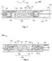
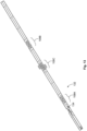
Fig. 1 , a perspective view of a detail of alighting module 100 according to an example not covered by the claims is shown. Thelighting module 100 comprises a flatflexible substrate 104 which is fabricated from an electrically insulating material, e.g. from polyimide, acrylate or a flexible ceramic material. Electrically conductive traces which form electricallyconductive leads 106 are patterned on the flatflexible substrate 104. Thelighting module 100 comprises a plurality of light emitting diodes (LED) 102 which are assembled as surface mount devices (SMD) and are electrically connected to the electrically conductive leads 106. - The
lighting module 100 has astretchable region 108 where the electrically conductive leads 106 are structured to form essentially U-shaped meander loops extending from afirst margin 110 to asecond margin 112 of the flatflexible substrate 104. Cut-outs 114 are provided which are partly encircled by the meander loops of the electrically conductive leads 106. This meander structure allows a bending around a curvature radius that lies within the plane of theflexible substrate 104 as indicated by thearrow 116, deforming the flatflexible substrate 104 laterally from its straight longitudinalmiddle axis 118. By providing only comparativelynarrow webs 120 at the margins, a sufficient degree of elasticity is generated that allows bending in the direction ofarrow 116. - The electrically
conductive lead 106 is formed within a metallization layer as a straight line separated bygaps 128 from aground plane layer 122. An electrically insulating protective layer is deposited to cover the electrically conductive layer. In order to lower the rigidity of thewebs 120, theground plane layer 122 is structured that it leaves open thewebs 120. - In addition to the
LEDs 102, thelighting module 100 further comprisescapacitors 124 which are also formed as SMD components. TheLEDs 102 advantageously are formed as a standard SMD LED package with four terminals (three anode terminals A and one cathode terminal C, the C terminal being marked by a beveled edge) as this is known in the art. -
Fig. 2 shows an example not covered by the claims of thelighting module 100. - According to this example, a
connector 126 for connecting thelighting module 100 to an external electronic component is provided on the flat flexible carrier. - By cutting away the webs 120 a further advantageous structure of the
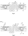
lighting module 100 is created. This modification is shown inFigures 3 and 4 . According to an example not covered by the claims, instead of theopenings 114 that are surrounded by theflexible substrate 104 on a closed circumference, slits 130 (also called incisions) are provided which are open at themargins flexible substrate 104 also has a meander structure that essentially follows the meander structure formed by the electricallyconductive lead 106. - As becomes apparent from
Fig. 4 , this configuration allows the flat flexible carrier (FFC) 132 being bent in thestretchable region 108 as indicated by thearrow 116, thus deforming the flat flexible carrier within the plane defined by theflexible substrate 104. The usual bending in directions which are across to the plane of theflexible substrate 104 is of course also possible, so that thelighting module 100 can be adapted to three-dimensionally complex carrier structures on which it has to be mounted. This is particularly advantageous for applications in a vehicle, such as backlights, brake lights, signaling, interior lighting, or headlights. - As shown in
Figures 5 to 7 , theconfiguration having incisions 130 advantageously is implemented by accordingly structuring theflexible substrate 104. The advantage thereof can be seen in the fact that no separate stamping step has to be performed. -
Figures 6 and 7 further illustrate that a bending within the plane defined by the flatflexible substrate 104 only takes place in thestretchable region 108. All remaining parts stay straight. InFig. 7 , theincisions 130A that are located at themargin 112, towards which the right-hand side part of thelighting module 100 is bent, are compressed, while theincisions 130B at theopposing margin 110 are stretched. In other words, by the bending process thefirst incisions 130A are closed at the margin, while thesecond incisions 130B are further opened. -
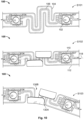
Figures 8 to 10 illustrate an embodiment of thelighting module 100 according to the present invention. According to this embodiment, in thestretchable region 108, the electrically conductive leads 106 and the flatflexible substrate 104 are shaped in a way that two of the meander loops extend further from the longitudinalmiddle axis 118 than themargins flexible substrate 104 in the remaining regions of thelighting module 100. However, it is clear for a person skilled in the art that the arrangement does not necessarily have to be symmetric with respect to the longitudinalmiddle axis 118 and that any suitable values for the distance D may be chosen. - The advantage of this arrangement can be seen in the fact that the
lighting module 100 may be expanded along thearrows 115, compressed as indicated by thearrows 117, but also angled as indicated by thearrow 116. - In case the
lighting module 100 according to the embodiment shown inFigures 8 and 9 has to be mounted in an area where there is not enough space for the additional distance D, the meander loop areas that are extending over themargins middle axis 118. This process is shown inFig. 10 . Instep S 101 thelighting module 100 is provided with the meander structure shown inFig. 8 . Next, the parts of the U-shaped meander loops that are extending further than themargins 110 112, are folded towards the longitudinal middle axis 118 (see step S 102). Finally, if needed, thelighting module 100 may be angled as shown in step S103. Thereby theincisions 130B are expanded, while theincisions 130A are compressed. - The various examples explained with reference to
Figures 1 to 7 may of course also be combined with the embodiment ofFig. 8 . Such a configuration is shown schematically inFig. 11 . According to this embodiment, eightLEDs 102 are arranged in a serial configuration. Electrically conductive leads 106 interconnect the LEDs with each other and/or acapacitor 124 and/or aconnector 126. Depending on the required degree of angling, three differentstretchable regions - It is clear for a person skilled in the art, that any other desirable combination of
stretchable regions 108 may of course also be implemented. -
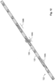
Fig. 12 and13 illustrate the layout of a flat flexible carrier (FFC) 132 for alighting module 100 having 12 LEDs and three differentstretchable regions Fig. 12 shows the first surface whereon the electric components and the LEDs are mounted, whileFig. 13 shows the opposing surface of theFFC 132.Vias 134 interconnect metallization layers of the first surface with metallization layers on the second surface. - In summary, the idea according to the present invention makes it possible to stretch and bend a flat flexible circuit board in the plane dimension. This allows more flexibility during installation of the flexible circuit and eliminates tension in the material due to different thermal expansion between the flexible circuit board and a carrier. Thereby the disadvantage of conventional flat straight flexible circuits can be overcome which can only be bent away from the plane surface but have no flexibility in the plane dimension.
- The invention proposes implementing meander structures into the flexible circuit design to achieve the required flexibility. The meander structures shown in
Fig. 8 , as well as combinations of the meander structures shown inFig. 1 and3 with that ofFig. 8 are part of this invention which can be used to provide a defined flexibility for different applications. Due to the meander structures in the flexible circuit board, it is possible to mount a flexible circuit board on a flat or curved surface with a certain angle or with a particular flexibility between two or more parts of the flexible circuit board. This allows a flexible circuit board that has been produced in a straight shape to be mounted on a carrier that follows a complex shape which has bends in more than one dimension. - The present invention can advantageously be used for dynamic lighting modules for transportation applications.
-
Reference Numeral Description 100 Lighting module 102 Light emitting element; LED 104 Flat flexible substrate 106 Electrically conductive lead 108 Stretchable region 110 First margin 112 Second margin 114 Cut-out 115,116, 117 Arrows symbolizing deformation 118 Longitudinal middle axis 120 Web 122 Ground plane layer 124 Capacitor 126 Electrical connector 128 Gap 130 Incision 132 Flat flexible carrier (FFC) 134 Via
Claims (11)
- A lighting module comprising:a flat flexible carrier, the flat flexible carrier comprising at least one electrically insulating flexible substrate (104) with a first surface and a second surface, and at least one planar electrically conductive lead (106) that is arranged on one of the first or second surfaces of said flexible substrate (104); andat least one light emitting element (102) and at least one electronic component (124), the light emitting element (102) and the electronic component (124, 126) and/or a second light emitting element (102) being electrically connected to each other by means of said at least one electrically conductive lead (106);wherein, in at least one stretchable region, which is part of the same flat flexible carrier, said conductive lead (106) is patterned to form at least one meander loop, which extends from the longitudinal middle axis (118) further than the first and second margin (110, 112) of the flat flexible carrier outside the stretchable region extending along the longitudinal middle axis, and said substrate (104) has at least one cut-out (114) which forms an incision that is open at the margin (110, 112) of the substrate (104) and that is provided adjacent to the meander loop in a way that the at least one meander loop partly encircles the cut-out (114),wherein the parts of the loops that extend further than the margins (110, 112) are folded back towards the longitudinal middle axis (118) of the flat flexible substrate (104), so that an essentially straight outline along the first and second margin (110, 112) is formed along the lighting module (100).
- The lighting module according to claim 1, wherein said at least one electronic component (124, 126) comprises at least one of a capacitor and an electrical connector to be connected to an external electronic component.
- The lighting module according to one of the preceding claims, wherein the at least one light emitting element (102) comprises a light emitting diode (LED).
- The lighting module according to one of the preceding claims, wherein the light emitting element (102) and/or the electronic component (124, 126) comprise a surface mount device (SMD).
- The lighting module according to one of the preceding claims, wherein the at least one electrically conductive (106) lead is covered at least partly by an electrically insulating protective layer (122).
- The lighting module according to one of the preceding claims, wherein said at least one electrically conductive lead (106) comprises a strip line separated from a grounding plane layer by gaps running in parallel to the strip line.
- The lighting module according to one of the preceding claims, wherein the electrically insulating flexible substrate is fabricated from polyimide, acrylate, or flexible ceramic, and/or wherein the at least one electrically conductive lead is fabricated from a metal or metal alloy or from a polymer filled with conductive particles.
- The lighting module according to one of the preceding claims, further comprising embedded rigid areas for assembling said light emitting element and/or the electronic component.
- The lighting module according to one of the preceding claims, wherein the at least one stretchable region separates regions where at least one light emitting element and/or electronic component are assembled.
- Method of fabricating a lighting module, the method comprising the steps of:fabricating a flat flexible carrier, the carrier comprising at least one electrically insulating flexible substrate (104) with a first surface and a second surface, and at least one planar electrically conductive lead (106) that is arranged on one of the first or second surfaces of said flexible substrate; andassembling at least one light emitting element (102) and at least one electronic component (124), the light emitting element and the electronic component and/or a second light emitting element being electrically connected to each other by means of said at least one electrically conductive lead; wherein, in at least one stretchable region, which is part of the same flat flexible carrier, said conductive lead is patterned to form at least one meander loop, and said substrate has at least one cut-out (114) which forms an incision that is open at the margin of the substrate and that is provided adjacent to the meander loop in a way that the at least one meander loop partly encircles the cut-out,wherein the flat flexible carrier outside the stretchable region has a first and second margin extending along the longitudinal middle axis, and wherein, in the stretchable region, the electrically conductive lead forms at least one meander loop that extends from the longitudinal middle axis further than the first and second margin, and wherein the method further comprises the step of folding back towards the centre of the flat flexible carrier the part of the loops that extends further than the margins, so that an essentially straight outline along the first and second margin is formed.
- Method according to claim 10, wherein the cut-out is formed by stamping the flat flexible carrier.
Priority Applications (2)
| Application Number | Priority Date | Filing Date | Title |
|---|---|---|---|
| EP16188098.4A EP3294046B1 (en) | 2016-09-09 | 2016-09-09 | Solid state lighting module and method of fabricating same |
| PCT/EP2017/072179 WO2018046474A1 (en) | 2016-09-09 | 2017-09-05 | Solid state lighting module and method of fabricating same |
Applications Claiming Priority (1)
| Application Number | Priority Date | Filing Date | Title |
|---|---|---|---|
| EP16188098.4A EP3294046B1 (en) | 2016-09-09 | 2016-09-09 | Solid state lighting module and method of fabricating same |
Publications (2)
| Publication Number | Publication Date |
|---|---|
| EP3294046A1 EP3294046A1 (en) | 2018-03-14 |
| EP3294046B1 true EP3294046B1 (en) | 2023-08-02 |
Family
ID=56896412
Family Applications (1)
| Application Number | Title | Priority Date | Filing Date |
|---|---|---|---|
| EP16188098.4A Active EP3294046B1 (en) | 2016-09-09 | 2016-09-09 | Solid state lighting module and method of fabricating same |
Country Status (2)
| Country | Link |
|---|---|
| EP (1) | EP3294046B1 (en) |
| WO (1) | WO2018046474A1 (en) |
Families Citing this family (4)
| Publication number | Priority date | Publication date | Assignee | Title |
|---|---|---|---|---|
| TWI797140B (en) * | 2018-06-25 | 2023-04-01 | 晶元光電股份有限公司 | Light emitting device with extendable and flexible carrier |
| RU2689297C1 (en) * | 2018-09-27 | 2019-05-27 | Федеральное государственное бюджетное учреждение "Национальный исследовательский центр "Курчатовский институт" | Method of synchronizing devices in electron synchrotrons of synchrotron radiation sources |
| JP7026367B1 (en) * | 2021-07-20 | 2022-02-28 | エレファンテック株式会社 | Wiring board and its manufacturing method |
| IT202100027629A1 (en) * | 2021-10-28 | 2023-04-28 | Linea Light S R L | LIGHT STRIP AND RELATED MANUFACTURING METHOD |
Family Cites Families (5)
| Publication number | Priority date | Publication date | Assignee | Title |
|---|---|---|---|---|
| GB2034102A (en) * | 1978-10-02 | 1980-05-29 | Xerox Corp | Flat cable |
| JP4932632B2 (en) * | 2007-08-06 | 2012-05-16 | 真也 石田 | Display system with flexible LED module |
| KR200448772Y1 (en) * | 2009-11-02 | 2010-05-17 | 백성곤 | Bendable LED Bar |
| US9337404B2 (en) * | 2011-03-22 | 2016-05-10 | Koninklijke Philips N.V. | Substrate for mounting a plurality of light emitting elements |
| DE102012100663A1 (en) * | 2012-01-26 | 2013-08-01 | Sumida Flexible Connections Gmbh | Flexible electrical connector |
-
2016
- 2016-09-09 EP EP16188098.4A patent/EP3294046B1/en active Active
-
2017
- 2017-09-05 WO PCT/EP2017/072179 patent/WO2018046474A1/en active Application Filing
Also Published As
| Publication number | Publication date |
|---|---|
| WO2018046474A1 (en) | 2018-03-15 |
| EP3294046A1 (en) | 2018-03-14 |
Similar Documents
| Publication | Publication Date | Title |
|---|---|---|
| EP3294046B1 (en) | Solid state lighting module and method of fabricating same | |
| US10943740B2 (en) | Electrical connection contact for a ceramic component, a ceramic component, and a component arrangement | |
| US10251261B2 (en) | Circuit structure | |
| CN101150121B (en) | Flexible circuits having improved reliability and thermal dissipation | |
| US10222036B2 (en) | Method and system for a three-dimensional (3-D) flexible light emitting diode (LED) bar | |
| CN102203504B (en) | Method for producing a flexible light strip | |
| US20160211473A1 (en) | Electrically interconnecting foil | |
| EP3305040B1 (en) | Lighting strip | |
| US20170003441A1 (en) | Light source circuit unit and lighting device comprising same | |
| JP2019216272A (en) | Flexible board | |
| CN102365491A (en) | Lighting system comprising at least one luminous band | |
| US9203009B2 (en) | Electrode module for LED lamp | |
| US7816691B2 (en) | Light-emitting diode having a flexible substrate | |
| JP2007073723A (en) | Fitting method for led and fitting structure for led | |
| US10477670B2 (en) | Flexible circuit board assembly for LED lamp | |
| EP3427555B1 (en) | A lighting device and corresponding method | |
| KR101300577B1 (en) | Led lamp for vehicle and the method thereof | |
| CN109076693A (en) | Flexible solid light band | |
| JP2022516582A (en) | Flexible printed circuit board assembly | |
| JP2007112299A (en) | Flexible wiring substrate for lighting system | |
| JP2012084590A (en) | Wiring circuit board and lighting fixture for vehicle using the same | |
| JP2011003595A (en) | Mounting wiring board for lighting, lighting device, and lighting fixture | |
| US11527689B2 (en) | Optoelectronic assembly, method and molded part | |
| JP2008270421A (en) | Thermoelectric module | |
| EP3450833B1 (en) | Electronic device and lighting module |
Legal Events
| Date | Code | Title | Description |
|---|---|---|---|
| PUAI | Public reference made under article 153(3) epc to a published international application that has entered the european phase |
Free format text: ORIGINAL CODE: 0009012 |
|
| STAA | Information on the status of an ep patent application or granted ep patent |
Free format text: STATUS: THE APPLICATION HAS BEEN PUBLISHED |
|
| AK | Designated contracting states |
Kind code of ref document: A1 Designated state(s): AL AT BE BG CH CY CZ DE DK EE ES FI FR GB GR HR HU IE IS IT LI LT LU LV MC MK MT NL NO PL PT RO RS SE SI SK SM TR |
|
| AX | Request for extension of the european patent |
Extension state: BA ME |
|
| STAA | Information on the status of an ep patent application or granted ep patent |
Free format text: STATUS: REQUEST FOR EXAMINATION WAS MADE |
|
| 17P | Request for examination filed |
Effective date: 20180912 |
|
| RBV | Designated contracting states (corrected) |
Designated state(s): AL AT BE BG CH CY CZ DE DK EE ES FI FR GB GR HR HU IE IS IT LI LT LU LV MC MK MT NL NO PL PT RO RS SE SI SK SM TR |
|
| STAA | Information on the status of an ep patent application or granted ep patent |
Free format text: STATUS: EXAMINATION IS IN PROGRESS |
|
| 17Q | First examination report despatched |
Effective date: 20210622 |
|
| STAA | Information on the status of an ep patent application or granted ep patent |
Free format text: STATUS: EXAMINATION IS IN PROGRESS |
|
| GRAP | Despatch of communication of intention to grant a patent |
Free format text: ORIGINAL CODE: EPIDOSNIGR1 |
|
| STAA | Information on the status of an ep patent application or granted ep patent |
Free format text: STATUS: GRANT OF PATENT IS INTENDED |
|
| INTG | Intention to grant announced |
Effective date: 20230320 |
|
| GRAS | Grant fee paid |
Free format text: ORIGINAL CODE: EPIDOSNIGR3 |
|
| GRAA | (expected) grant |
Free format text: ORIGINAL CODE: 0009210 |
|
| STAA | Information on the status of an ep patent application or granted ep patent |
Free format text: STATUS: THE PATENT HAS BEEN GRANTED |
|
| AK | Designated contracting states |
Kind code of ref document: B1 Designated state(s): AL AT BE BG CH CY CZ DE DK EE ES FI FR GB GR HR HU IE IS IT LI LT LU LV MC MK MT NL NO PL PT RO RS SE SI SK SM TR |
|
| REG | Reference to a national code |
Ref country code: GB Ref legal event code: FG4D |
|
| REG | Reference to a national code |
Ref country code: CH Ref legal event code: EP |
|
| REG | Reference to a national code |
Ref country code: DE Ref legal event code: R096 Ref document number: 602016081535 Country of ref document: DE |
|
| REG | Reference to a national code |
Ref country code: IE Ref legal event code: FG4D |
|
| REG | Reference to a national code |
Ref country code: LT Ref legal event code: MG9D |
|
| PGFP | Annual fee paid to national office [announced via postgrant information from national office to epo] |
Ref country code: FR Payment date: 20230721 Year of fee payment: 8 Ref country code: DE Payment date: 20230726 Year of fee payment: 8 |
|
| REG | Reference to a national code |
Ref country code: NL Ref legal event code: MP Effective date: 20230802 |
|
| REG | Reference to a national code |
Ref country code: AT Ref legal event code: MK05 Ref document number: 1596323 Country of ref document: AT Kind code of ref document: T Effective date: 20230802 |
|
| PG25 | Lapsed in a contracting state [announced via postgrant information from national office to epo] |
Ref country code: GR Free format text: LAPSE BECAUSE OF FAILURE TO SUBMIT A TRANSLATION OF THE DESCRIPTION OR TO PAY THE FEE WITHIN THE PRESCRIBED TIME-LIMIT Effective date: 20231103 |
|
| PG25 | Lapsed in a contracting state [announced via postgrant information from national office to epo] |
Ref country code: IS Free format text: LAPSE BECAUSE OF FAILURE TO SUBMIT A TRANSLATION OF THE DESCRIPTION OR TO PAY THE FEE WITHIN THE PRESCRIBED TIME-LIMIT Effective date: 20231202 |
|
| PG25 | Lapsed in a contracting state [announced via postgrant information from national office to epo] |
Ref country code: SE Free format text: LAPSE BECAUSE OF FAILURE TO SUBMIT A TRANSLATION OF THE DESCRIPTION OR TO PAY THE FEE WITHIN THE PRESCRIBED TIME-LIMIT Effective date: 20230802 Ref country code: RS Free format text: LAPSE BECAUSE OF FAILURE TO SUBMIT A TRANSLATION OF THE DESCRIPTION OR TO PAY THE FEE WITHIN THE PRESCRIBED TIME-LIMIT Effective date: 20230802 Ref country code: PT Free format text: LAPSE BECAUSE OF FAILURE TO SUBMIT A TRANSLATION OF THE DESCRIPTION OR TO PAY THE FEE WITHIN THE PRESCRIBED TIME-LIMIT Effective date: 20231204 Ref country code: NO Free format text: LAPSE BECAUSE OF FAILURE TO SUBMIT A TRANSLATION OF THE DESCRIPTION OR TO PAY THE FEE WITHIN THE PRESCRIBED TIME-LIMIT Effective date: 20231102 Ref country code: NL Free format text: LAPSE BECAUSE OF FAILURE TO SUBMIT A TRANSLATION OF THE DESCRIPTION OR TO PAY THE FEE WITHIN THE PRESCRIBED TIME-LIMIT Effective date: 20230802 Ref country code: LV Free format text: LAPSE BECAUSE OF FAILURE TO SUBMIT A TRANSLATION OF THE DESCRIPTION OR TO PAY THE FEE WITHIN THE PRESCRIBED TIME-LIMIT Effective date: 20230802 Ref country code: LT Free format text: LAPSE BECAUSE OF FAILURE TO SUBMIT A TRANSLATION OF THE DESCRIPTION OR TO PAY THE FEE WITHIN THE PRESCRIBED TIME-LIMIT Effective date: 20230802 Ref country code: IS Free format text: LAPSE BECAUSE OF FAILURE TO SUBMIT A TRANSLATION OF THE DESCRIPTION OR TO PAY THE FEE WITHIN THE PRESCRIBED TIME-LIMIT Effective date: 20231202 Ref country code: HR Free format text: LAPSE BECAUSE OF FAILURE TO SUBMIT A TRANSLATION OF THE DESCRIPTION OR TO PAY THE FEE WITHIN THE PRESCRIBED TIME-LIMIT Effective date: 20230802 Ref country code: GR Free format text: LAPSE BECAUSE OF FAILURE TO SUBMIT A TRANSLATION OF THE DESCRIPTION OR TO PAY THE FEE WITHIN THE PRESCRIBED TIME-LIMIT Effective date: 20231103 Ref country code: FI Free format text: LAPSE BECAUSE OF FAILURE TO SUBMIT A TRANSLATION OF THE DESCRIPTION OR TO PAY THE FEE WITHIN THE PRESCRIBED TIME-LIMIT Effective date: 20230802 Ref country code: AT Free format text: LAPSE BECAUSE OF FAILURE TO SUBMIT A TRANSLATION OF THE DESCRIPTION OR TO PAY THE FEE WITHIN THE PRESCRIBED TIME-LIMIT Effective date: 20230802 |
|
| PG25 | Lapsed in a contracting state [announced via postgrant information from national office to epo] |
Ref country code: PL Free format text: LAPSE BECAUSE OF FAILURE TO SUBMIT A TRANSLATION OF THE DESCRIPTION OR TO PAY THE FEE WITHIN THE PRESCRIBED TIME-LIMIT Effective date: 20230802 |