EP3293758A1 - A sequential integration process - Google Patents
A sequential integration process Download PDFInfo
- Publication number
- EP3293758A1 EP3293758A1 EP17190841.1A EP17190841A EP3293758A1 EP 3293758 A1 EP3293758 A1 EP 3293758A1 EP 17190841 A EP17190841 A EP 17190841A EP 3293758 A1 EP3293758 A1 EP 3293758A1
- Authority
- EP
- European Patent Office
- Prior art keywords
- wafer
- device region
- layer
- semiconductor
- forming
- Prior art date
- Legal status (The legal status is an assumption and is not a legal conclusion. Google has not performed a legal analysis and makes no representation as to the accuracy of the status listed.)
- Granted
Links
Images


Classifications
-
- H—ELECTRICITY
- H10—SEMICONDUCTOR DEVICES; ELECTRIC SOLID-STATE DEVICES NOT OTHERWISE PROVIDED FOR
- H10F—INORGANIC SEMICONDUCTOR DEVICES SENSITIVE TO INFRARED RADIATION, LIGHT, ELECTROMAGNETIC RADIATION OF SHORTER WAVELENGTH OR CORPUSCULAR RADIATION
- H10F39/00—Integrated devices, or assemblies of multiple devices, comprising at least one element covered by group H10F30/00, e.g. radiation detectors comprising photodiode arrays
- H10F39/10—Integrated devices
- H10F39/12—Image sensors
- H10F39/15—Charge-coupled device [CCD] image sensors
- H10F39/157—CCD or CID infrared image sensors
-
- H—ELECTRICITY
- H10—SEMICONDUCTOR DEVICES; ELECTRIC SOLID-STATE DEVICES NOT OTHERWISE PROVIDED FOR
- H10D—INORGANIC ELECTRIC SEMICONDUCTOR DEVICES
- H10D64/00—Electrodes of devices having potential barriers
- H10D64/20—Electrodes characterised by their shapes, relative sizes or dispositions
- H10D64/23—Electrodes carrying the current to be rectified, amplified, oscillated or switched, e.g. sources, drains, anodes or cathodes
- H10D64/231—Emitter or collector electrodes for bipolar transistors
-
- H—ELECTRICITY
- H10—SEMICONDUCTOR DEVICES; ELECTRIC SOLID-STATE DEVICES NOT OTHERWISE PROVIDED FOR
- H10D—INORGANIC ELECTRIC SEMICONDUCTOR DEVICES
- H10D84/00—Integrated devices formed in or on semiconductor substrates that comprise only semiconducting layers, e.g. on Si wafers or on GaAs-on-Si wafers
- H10D84/01—Manufacture or treatment
- H10D84/02—Manufacture or treatment characterised by using material-based technologies
- H10D84/03—Manufacture or treatment characterised by using material-based technologies using Group IV technology, e.g. silicon technology or silicon-carbide [SiC] technology
- H10D84/038—Manufacture or treatment characterised by using material-based technologies using Group IV technology, e.g. silicon technology or silicon-carbide [SiC] technology using silicon technology, e.g. SiGe
-
- H—ELECTRICITY
- H10—SEMICONDUCTOR DEVICES; ELECTRIC SOLID-STATE DEVICES NOT OTHERWISE PROVIDED FOR
- H10D—INORGANIC ELECTRIC SEMICONDUCTOR DEVICES
- H10D84/00—Integrated devices formed in or on semiconductor substrates that comprise only semiconducting layers, e.g. on Si wafers or on GaAs-on-Si wafers
- H10D84/01—Manufacture or treatment
- H10D84/02—Manufacture or treatment characterised by using material-based technologies
- H10D84/08—Manufacture or treatment characterised by using material-based technologies using combinations of technologies, e.g. using both Si and SiC technologies or using both Si and Group III-V technologies
-
- H—ELECTRICITY
- H10—SEMICONDUCTOR DEVICES; ELECTRIC SOLID-STATE DEVICES NOT OTHERWISE PROVIDED FOR
- H10D—INORGANIC ELECTRIC SEMICONDUCTOR DEVICES
- H10D88/00—Three-dimensional [3D] integrated devices
-
- H—ELECTRICITY
- H10—SEMICONDUCTOR DEVICES; ELECTRIC SOLID-STATE DEVICES NOT OTHERWISE PROVIDED FOR
- H10D—INORGANIC ELECTRIC SEMICONDUCTOR DEVICES
- H10D88/00—Three-dimensional [3D] integrated devices
- H10D88/01—Manufacture or treatment
-
- H—ELECTRICITY
- H10—SEMICONDUCTOR DEVICES; ELECTRIC SOLID-STATE DEVICES NOT OTHERWISE PROVIDED FOR
- H10F—INORGANIC SEMICONDUCTOR DEVICES SENSITIVE TO INFRARED RADIATION, LIGHT, ELECTROMAGNETIC RADIATION OF SHORTER WAVELENGTH OR CORPUSCULAR RADIATION
- H10F77/00—Constructional details of devices covered by this subclass
- H10F77/30—Coatings
- H10F77/306—Coatings for devices having potential barriers
- H10F77/331—Coatings for devices having potential barriers for filtering or shielding light, e.g. multicolour filters for photodetectors
- H10F77/334—Coatings for devices having potential barriers for filtering or shielding light, e.g. multicolour filters for photodetectors for shielding light, e.g. light blocking layers or cold shields for infrared detectors
-
- H—ELECTRICITY
- H10—SEMICONDUCTOR DEVICES; ELECTRIC SOLID-STATE DEVICES NOT OTHERWISE PROVIDED FOR
- H10W—GENERIC PACKAGES, INTERCONNECTIONS, CONNECTORS OR OTHER CONSTRUCTIONAL DETAILS OF DEVICES COVERED BY CLASS H10
- H10W20/00—Interconnections in chips, wafers or substrates
- H10W20/01—Manufacture or treatment
- H10W20/021—Manufacture or treatment of interconnections within wafers or substrates
- H10W20/023—Manufacture or treatment of interconnections within wafers or substrates the interconnections being through-semiconductor vias
-
- H—ELECTRICITY
- H10—SEMICONDUCTOR DEVICES; ELECTRIC SOLID-STATE DEVICES NOT OTHERWISE PROVIDED FOR
- H10W—GENERIC PACKAGES, INTERCONNECTIONS, CONNECTORS OR OTHER CONSTRUCTIONAL DETAILS OF DEVICES COVERED BY CLASS H10
- H10W20/00—Interconnections in chips, wafers or substrates
- H10W20/01—Manufacture or treatment
- H10W20/021—Manufacture or treatment of interconnections within wafers or substrates
- H10W20/023—Manufacture or treatment of interconnections within wafers or substrates the interconnections being through-semiconductor vias
- H10W20/0242—Manufacture or treatment of interconnections within wafers or substrates the interconnections being through-semiconductor vias comprising etching via holes from the back sides of the chips, wafers or substrates
-
- H—ELECTRICITY
- H10—SEMICONDUCTOR DEVICES; ELECTRIC SOLID-STATE DEVICES NOT OTHERWISE PROVIDED FOR
- H10W—GENERIC PACKAGES, INTERCONNECTIONS, CONNECTORS OR OTHER CONSTRUCTIONAL DETAILS OF DEVICES COVERED BY CLASS H10
- H10W20/00—Interconnections in chips, wafers or substrates
- H10W20/01—Manufacture or treatment
- H10W20/021—Manufacture or treatment of interconnections within wafers or substrates
- H10W20/023—Manufacture or treatment of interconnections within wafers or substrates the interconnections being through-semiconductor vias
- H10W20/0245—Manufacture or treatment of interconnections within wafers or substrates the interconnections being through-semiconductor vias comprising use of blind vias during the manufacture
-
- B—PERFORMING OPERATIONS; TRANSPORTING
- B28—WORKING CEMENT, CLAY, OR STONE
- B28D—WORKING STONE OR STONE-LIKE MATERIALS
- B28D1/00—Working stone or stone-like materials, e.g. brick, concrete or glass, not provided for elsewhere; Machines, devices, tools therefor
- B28D1/005—Cutting sheet laminae in planes between faces
-
- H—ELECTRICITY
- H10—SEMICONDUCTOR DEVICES; ELECTRIC SOLID-STATE DEVICES NOT OTHERWISE PROVIDED FOR
- H10D—INORGANIC ELECTRIC SEMICONDUCTOR DEVICES
- H10D88/00—Three-dimensional [3D] integrated devices
- H10D88/101—Three-dimensional [3D] integrated devices comprising components on opposite major surfaces of semiconductor substrates
-
- H—ELECTRICITY
- H10—SEMICONDUCTOR DEVICES; ELECTRIC SOLID-STATE DEVICES NOT OTHERWISE PROVIDED FOR
- H10F—INORGANIC SEMICONDUCTOR DEVICES SENSITIVE TO INFRARED RADIATION, LIGHT, ELECTROMAGNETIC RADIATION OF SHORTER WAVELENGTH OR CORPUSCULAR RADIATION
- H10F77/00—Constructional details of devices covered by this subclass
- H10F77/20—Electrodes
- H10F77/206—Electrodes for devices having potential barriers
-
- H—ELECTRICITY
- H10—SEMICONDUCTOR DEVICES; ELECTRIC SOLID-STATE DEVICES NOT OTHERWISE PROVIDED FOR
- H10P—GENERIC PROCESSES OR APPARATUS FOR THE MANUFACTURE OR TREATMENT OF DEVICES COVERED BY CLASS H10
- H10P52/00—Grinding, lapping or polishing of wafers, substrates or parts of devices
Definitions
- the present inventive concept relates to a sequential integration process.
- a conventional 3D integration process also known as chip-stacking, involves stacking and bonding of two or more processed wafers on top of each other and interconnecting the devices of the processed wafers by vias.
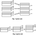
- a prior art 3D integration process is schematically illustrated in Fig. 1 wherein three processed wafers 10, 20 and 30, each having a semiconductor device region 12, 22, 32 and an interconnection layer 14, 24, 34, are stacked and bonded to each other via an oxide or nitride bonding layer 16, 26, 36. Different levels of the stack may be connected by vias.
- FIG. 2 A prior art sequential 3D integration process is schematically illustrated in Fig. 2 wherein a semiconductor substrate 50 is transferred on top of a wafer 40 having a semiconductor device region 42, an interconnection layer 44 and a bonding layer 46. Processing for forming a semiconductor device region 52 on the front side of the semiconductor substrate 50 is then performed. An interconnection layer 54 may be formed on the semiconductor device region 52. Different levels of the stack may be connected by vias.
- 3D integration processes allow forming of area efficient chips or integrated circuits.
- the sequential 3D integration process provides the additional benefit over the conventional integration process of enabling reduced device layer spacing and via height compared to the chip-stacking technique since the wafer 40 supports the substrate 50 during the device processing on the substrate 50 and hence reduces the number of wafers needed.
- the wafer 40 supports the substrate 50 during the device processing on the substrate 50 and hence reduces the number of wafers needed.
- An objective of the present inventive concept is to provide a sequential integration process enabling a further improvement in area efficiency of manufactured circuits compared to the prior art integration processes. Additional or alternative objectives may be understood from the following.
- an additional wafer surface namely the backside of the first wafer is made available for device integration. Accordingly a vertical wafer stack including a first wafer with both front and back side device regions may be formed. For a same number of wafers, this enables manufacturing of circuits of an improved area efficiency compared to the prior art processes.
- the inventive process may be referred to as a "sequential" integration process.
- a "front side” and a “back side” of a wafer means opposite sides of the wafer, or in other words the sides formed by mutually opposite first and second main surfaces of the wafer.
- Forming or bonding a region/layer "on", or a region/layer being formed or bonded "to", a front/back side of a wafer may accordingly herein be understood as forming said region/layer, or said region/layer being formed or bonded, directly on the front/back side surface of the wafer (i.e. without any intermediate layers) or on the front/back side surface of the wafer with one or more intermediate layers between the front/back side surface of the wafer and the region/layer formed (i.e. the region/layer formed "at" the front/back side surface of the wafer).
- a “device region” (e.g. the first or the second device region) is herein meant a region having a lateral or horizontal extension on a wafer or substrate side.
- a device region may also be referred to as an active device region.
- a device region of a wafer or substrate may form a front end of line (FEOL) device region of the wafer or substrate.
- FEOL front end of line
- a device region may include a set of planar or non-planar semiconductor devices, or a combination thereof.
- a thickness portion of a wafer or substrate, in which a device region is formed is formed may be referred to as a device layer, an active device layer, or a FEOL (device) layer of the wafer / substrate.
- Dielectric regions may be formed in a semiconductor wafer or semiconductor substrate for device isolation. Dielectric regions may be formed by shallow-trench isolation (STI) regions. Dielectric regions may be formed before a device region has been formed, after a device region has been formed or between device region processing steps.
- STI shallow-trench isolation
- the first device region may be formed by processing the front side of the first wafer to form the semiconductor devices in semiconductor material of the front side of the first wafer.
- the second device region may be formed by processing the back side of the first wafer to form the semiconductor devices in semiconductor material of the back side of the first wafer.
- the second device region may be formed by processing a semiconductor layer bonded to the back side of the first wafer to form the semiconductor devices in the semiconductor layer.
- the first device region and the second device region may include devices of different types. Devices may be formed of different semiconductor materials, include different combinations of dopants, and/or include different dopant concentrations.
- interconnection layer is herein meant one or more dielectric layers including conducting patterns or paths.
- a plurality of interconnection layers may be present including a plurality of interconnection levels (formed by conducting patterned layers) separated by inter-level dielectrics. Conductive paths of both inter- and intra-layer extension may be present.
- the conducting paths may electrically interconnect the semiconductor devices of a device region and optionally also interconnect contact regions (e.g. source, drain or gate) of individual semiconductor devices.
- the at least one interconnection layer may form middle end of line (MOL) and/or back end of line (BEOL) layers.
- MOL middle end of line
- BEOL back end of line
- At least one "via” is herein meant at least one electrical connection extending in a vertical direction through the wafer stack.
- One or more of the vias may extend completely or at least partially through the first wafer.
- One or more of the vias may extend through a semiconductor portion of the first wafer and/or a dielectric/STI region of the first wafer (if such are present).
- One or more of the vias may form "inter-tier” vias. That is, the vias may interconnect device regions and/or interconnection layers at different "tiers" or "levels" of the wafer stack.
- One or more of the vias may form through substrate vias or through silicon vias (TSVs) with respect to at least the first wafer of the stack.
- TSVs through silicon vias
- One or more of the vias may extend from the at least one interconnection layer and at least to the first device region.
- One or more of the vias may electrically connect the at least one interconnection layer to one or more of the first device region and the second device region.
- Bonding of the first wafer to the second wafer may include bonding the first wafer and the second wafer via an intermediate bonding layer.
- a bonding layer may be formed on one or more of the wafer sides facing each other.
- a bonding layer may be an oxide layer wherein the wafers may be bonded by oxide-oxide bonding.
- a bonding layer may be a nitride layer wherein the wafers may be bonded by nitride-nitride bonding. Electrical insulation between wafers may thereby be achieved.
- the method further comprises bonding a semiconductor layer to the back side of the first wafer with a front side of said semiconductor layer facing the back side of the first wafer, wherein the forming of the second device region includes forming the second device region on a back side of said semiconductor layer.
- the second device region may accordingly be formed on the backside of the first wafer with at least a thickness portion of a semiconductor layer intermediate the first wafer and the second device region.
- hetero-integration is enabled, i.e. integration of different material systems in the wafer stack.
- the at least one interconnection layer formed on the second device region of the semiconductor layer may form MOL and/or BEOL layers of the semiconductor layer, i.e. with respect to the second device region.
- One or more of the vias may extend from the at least one interconnection layer, through the semiconductor layer and the first wafer.
- One or more of the vias may extend to the first device region of the first wafer and optionally also to an interconnection layer formed on the first device region of the first wafer (if such a layer is present).
- One or more of the vias may electrically connect the at least one interconnection layer formed on the second device region to one of more of the first device region, an interconnection layer formed on the first device region and the second device region.
- the semiconductor material forming the semiconductor devices of the second device region may be different from a semiconductor material forming the semiconductor devices of the first device region.
- the first device region includes Si semiconductor devices and the second device region includes Ge or group III-V semiconductor material devices, or vice versa.
- Different device technology may be implemented in the first device region and the second device region, for instance a combination of analog devices and digital devices, combinations of I/O devices, radio frequency (RF) devices and/or ESD devices (i.e. devices for protection from electrostatic discharge). It is also possible to form planar transistors in one of the device regions and non-planar transistors (e.g. FinFETs or nanowire transistors) in the other device region. It is also possible to form devices in the device regions using different process technology nodes, for instance the N45 node in one of the device regions and the N14 node in the other device region. Using slower nodes for implementing devices / circuitry for slower applications may reduce overall costs.
- the semiconductor layer (which also may be referred to as a semiconductor substrate) may be formed on a bottom substrate. Subsequent to the bonding of the semiconductor layer to the first wafer, the bottom substrate may be removed from said semiconductor layer to expose the back side of the semiconductor layer and thereafter the second device region may be formed on the back side of said semiconductor layer.
- the bottom substrate may thereby function as a handling or donor wafer for the semiconductor layer and thus facilitate transfer of a comparably thin semiconductor layer to the wafer stack.
- the act of forming the semiconductor layer on the bottom substrate may form part of the inventive process, or a semiconductor layer may be formed on a bottom substrate in a process separate from the inventive process and provided as pre-made component to the inventive process.
- thinning of the semiconductor layer may be performed.
- the height of the final stack may be reduced and any defective portions of the semiconductor layer may be removed. Also, an appropriate layer thickness for the intended device type may be obtained.
- the bottom substrate may include a Si-layer and the semiconductor layer may be formed by a group IV material layer.
- the group IV material layer may be formed by Ge, SiGe, SiC, or GeSn.
- a group IV material layer (i.e. other than Si) may be grown on the Si bottom substrate with or without an intermediate strain relaxed buffer (SRB).
- the bottom substrate may include a Si-layer and the semiconductor layer may be formed by a group III-V material layer or by a stack including a group III-V material layer formed on a Ge-layer.
- the group III-V material layer may be formed by AlAs, GaN, AlGaN, InN, AlN, GaP, GaAs, InP, InAs, InGaAs, InAlAs, InGaP, InSb, AlSb or InGaSb.
- a Ge-layer may be grown on a Si bottom substrate with or without an intermediate SRB.
- a group III-V material layer may grown on a Ge-layer with or without an intermediate SRB.
- a group III-V material layer enables forming of semiconductor devices with increased cut-off frequency compared to group IV materials.
- a group III-V material layer thus lends itself favorably to supporting a device region implementing RF devices.
- a group III-V material layer also offers improved electron mobility compared to group IV materials.
- a group III-V material layer thus lends itself favorably also to supporting a device region implementing NMOS devices.
- Forming the semiconductor layer as a stack of a Ge-layer and a group III-V material layer enables device regions including Ge- and group III-V semiconductor devices to be formed on opposite sides of the semiconductor layer.
- the device region on the Ge-layer may include PMOS devices (Ge presents advantageous hole mobility).
- the device region on the group III-V material layer may include NMOS devices (III-V materials present advantageous electron mobility).
- a third device region including a set of semiconductor devices may be formed on the front side of said semiconductor layer.
- the third device region may be formed prior to the bonding of said semiconductor layer to the first wafer.
- the act of forming the third device region may form part of the inventive process, or a third device region may be formed on the front side of the semiconductor layer in a process separate from the inventive process wherein a semiconductor substrate with a front side device region may be provided as a pre-made component to the process.
- the second and the third device region may form two mutually opposite FEOL device regions / layers of the semiconductor layer.
- the third device region may include a set of planar or non-planar semiconductor devices, or a combination thereof.
- the second device region and the third device region may include devices of different types. Devices may include different combinations of dopants, and/or include different dopant concentrations. The devices may be formed using different process technology nodes.
- At least one interconnection layer may be formed on the third device region for electrically interconnecting the semiconductor devices of the third device region.
- the at least one interconnection layer may form MOL and/or BEOL layers of the semiconductor substrate, i.e. with respect to the third device region.
- the act of forming the at least one interconnection layer on the third device region may form part of the inventive process, or at least one interconnection layer may be formed on the third device region of the semiconductor layer in a process separate from the inventive process wherein a semiconductor substrate with a front side device region and an interconnection layer may be provided as a pre-made component to the inventive process.
- the first wafer may be formed of a semiconductor material, for instance Si, Ge, SiGe, SiC, GaAs or InP.
- the first wafer may also be a SOI wafer, a GeOI wafer, SiGeOI wafer or a III-V-OI wafer.
- the second wafer may be formed of a semiconductor material, for instance Si, Ge, SiGe, SiC, GaAs, InP.
- the second wafer may also be a SOI wafer, a GeOI wafer, SiGeOI wafer, or a III-V-OI wafer.
- the second wafer may also be formed of a non-semiconductor material such as a dielectric material, advantageously a glass material.
- a device region including a set of semiconductor devices may be formed on the front side of the second wafer. It is hence possible to obtain a wafer stack wherein as many as four different device regions are formed on different levels of the stack of the second wafer/first wafer/semiconductor substrate, i.e. on the front side of the second wafer, on the front side of the first wafer, on the front side of the semiconductor layer and on the backside of the semiconductor layer.
- At least one interconnection layer may be formed on the device region of the second wafer for electrically interconnecting the semiconductor devices of the device region of the second wafer.
- the forming of the at least one interconnection layer may be performed prior to the bonding of the first wafer to the second wafer.
- the at least one interconnection layer may form MOL and/or BEOL layers of the second wafer, i.e. with respect to the device region formed on the second wafer.
- the act of forming a device region on the front side of the second wafer and/or the act of forming the at least one interconnection layer on the device region of the second wafer may form part of the inventive process, or a device region and/or at least one interconnection layer may be formed on the second wafer in a process separate from the inventive process wherein a second wafer with a front side device region and optionally also an interconnection layer may be provided as a pre-made component to the process.
- One or more of the vias may extend from the at least one interconnection layer formed on the second device region, through the semiconductor layer, the first wafer and to the device region of the second wafer or at least to an interconnection layer formed on the device region of the second wafer (if such a layer is present).
- One or more of the vias may electrically connect the at least one interconnection layer formed on the second device region to one of more of the first device region, an interconnection layer formed on the first device region, the second device region, the device region formed on the second wafer, and an interconnection layer formed on the device region of the second wafer (if such a layer is present).
- the second wafer may serve as a handling wafer and facilitate handling of the wafer stack during the process.
- the second wafer may be removed or thinned subsequent to forming of the interconnection layer on the second device region of the semiconductor layer. Removing or thinning of the second wafer may include grinding, CMP and/or etch back from the backside of the second wafer.
- the first wafer includes a semiconductor layer, wherein the first device region is formed on a front side of said semiconductor layer and bonding the first wafer to the second wafer includes bonding the front side of the semiconductor layer to the second wafer, and the method further comprises, subsequent to said bonding to the second wafer, forming the second device region on a back side of said semiconductor layer.
- the second device region may accordingly be formed directly on the backside of the first wafer, the backside being formed by the semiconductor layer.
- hetero-integration is enabled, i.e. integration of different material systems in the stack.
- the first and the second device region may form two mutually opposite FEOL device regions / layers of the semiconductor layer.
- At least one interconnection layer may be formed on the first device region for electrically interconnecting the semiconductor devices of the first device region.
- the at least one interconnection layer may form MOL and/or BEOL layers of the semiconductor layer, i.e. with respect to the first device region.
- the act of forming the at least one interconnection layer on the first device region may form part of the inventive process, or at least one interconnection layer may be formed on the first device region of the semiconductor layer in a process separate from the inventive process wherein a first wafer with a front side device region and an interconnection layer may be provided as a pre-made component to the process.
- the second wafer may be formed of a semiconductor material, for instance Si, Ge, SiGe, SiC, GaAs, InP.
- the second wafer may also be a SOI wafer, a GeOI wafer, SiGeOI wafer, or a III-V-OI wafer.
- the second wafer may also be formed of a non-semiconductor material such as a dielectric material, advantageously a glass material.
- a device region including a set of semiconductor devices may be formed on the front side of the second wafer.
- the device region of the second wafer may include a set of planar or non-planar semiconductor devices, or a combination thereof.
- the device region of the second wafer may include devices of types different from the first and second device regions of the semiconductor layer.
- Devices may be formed of different semiconductor materials, include different combinations of dopants, and/or include different dopant concentrations.
- the devices may be formed using different process technology nodes.
- At least one interconnection layer may be formed on the device region of the second wafer for electrically interconnecting the semiconductor devices of the device region of the second wafer.
- the forming of the at least one interconnection layer may be performed prior to the bonding of the first wafer to the second wafer.
- the at least one interconnection layer may form MOL and/or BEOL layers of the second wafer, i.e. with respect to the device region formed on the second wafer.
- the act of forming a device region on the front side of the second wafer and/or the act of forming the at least one interconnection layer on the device region of the second wafer may form part of the inventive process, or a device region and/or at least one interconnection layer may be formed on the second wafer in a process separate from the inventive process wherein a second wafer with a front side device region and optionally also an interconnection layer may be provided as a pre-made component to the process.
- the semiconductor material forming the semiconductor devices of the first and the second device region of the first wafer may be formed by a semiconductor material which is different from a semiconductor material forming the semiconductor devices of the device region of the second wafer. Accordingly different device technology may be implemented in the first/second device region of the semiconductor layer/first wafer and the device region of the second wafer, for instance a combination of analog devices and digital devices, combinations of I/O devices, RF devices and/or ESD devices. It is also possible to form planar transistors in at least one of the device regions and non-planar transistors (e.g. FinFETs or nanowire transistors) in at least one of the other device region(s).
- planar transistors in at least one of the device regions and non-planar transistors (e.g. FinFETs or nanowire transistors) in at least one of the other device region(s).
- the first wafer may further include a bottom substrate, the back side of the semiconductor layer facing the bottom substrate, wherein the method may further comprise, subsequent to said bonding to the second wafer, removing the bottom substrate from said semiconductor layer to expose the back side of the semiconductor layer and thereafter forming the second device region on the back side of said semiconductor layer.
- the bottom substrate may include a Si-layer and the semiconductor layer may be formed by a group IV material layer.
- the group IV material layer may be formed by Ge, SiGe, SiC, or GeSn.
- a group IV material layer (i.e. other than Si) may be grown on the Si bottom substrate with or without an intermediate SRB.
- the bottom substrate may include a Si-layer and the semiconductor layer may be formed by a group III-V material layer or by a stack including a group III-V material layer formed on a Ge-layer.
- the group III-V material layer may be formed by AlAs, GaN, AlGaN, InN, AIN, GaP, GaAs, InP, InAs, InGaAs, InAlAs, InGaP, InSb, AlSb or InGaSb.
- a Ge-layer may be grown on a Si bottom substrate with or without an intermediate SRB.
- a group III-V material layer may grown on a Ge-layer with or without an intermediate SRB.
- a group III-V material layer enables forming of semiconductor devices with increased cut-off frequency compared to group IV materials.
- a group III-V material layer thus lends itself favorably to supporting a device region implementing RF devices.
- a group III-V material layer also offers improved electron mobility compared to group IV materials.
- a group III-V material layer thus lends itself favorably also to supporting a device region implementing NMOS devices.
- Forming the semiconductor layer as a stack of a Ge-layer and a group III-V material layer enables device regions including Ge- and group III-V semiconductor devices to be formed on opposite sides of the semiconductor layer.
- the device region on the Ge-layer may include PMOS devices (Ge presents advantageous hole mobility).
- the device region on the group III-V material layer may include NMOS devices (III-V materials present advantageous electron mobility).
- One or more of the vias may extend from the at least one interconnection layer formed on the second device region, through the semiconductor layer of the first wafer, and to the device region of the second wafer or at least to an interconnection layer formed on the device region of the second wafer (if such a layer is present).
- One or more of the vias may electrically connect the at least one interconnection layer formed on the second device region to one of more of the first device region, an interconnection layer formed on the first device region, the second device region, the device region formed on the second wafer, and an interconnection layer formed on the device region of the second wafer (if such a layer is present).
- the forming of the second device region includes forming the second device region directly on the back side of the first wafer. Hence no separate dedicated handling wafer for supporting a layer / substrate implementing the second device region is required.
- This embodiment advantageously lends itself for homo-integration since a same wafer, i.e. the first wafer, implements both the first and the second device region.
- the first and the second device region may form two mutually opposite FEOL device regions / layers of the first wafer.
- thinning of the first wafer may be performed wherein the second device region may be formed on the back side of the thinned first wafer.
- Thinning of the first wafer may include performing a CMP on the backside of the first wafer.
- the first wafer may be formed of a semiconductor material, for instance Si, Ge, SiGe, SiC, GaAs, InP.
- the first wafer may also be a SOI wafer, a GeOI wafer, SiGeOI wafer or a III-V-OI wafer.
- the second wafer may be formed of a semiconductor material, for instance Si, Ge, SiGe, SiC, GaAs, InP.
- the second wafer may also be a SOI wafer, a GeOI wafer, SiGeOI wafer, or a III-V-OI wafer.
- the second wafer may also be formed of a non-semiconductor material such as a dielectric material, advantageously a glass material.
- a device region including a set of semiconductor devices may be formed on the front side of the second wafer.
- the device region of the second wafer may include a set of planar or non-planar semiconductor devices, or a combination thereof.
- the device region of the second wafer may include devices of types different from the first and second device regions of the semiconductor layer.
- Devices may be formed of different semiconductor materials, include different combinations of dopants, and/or include different dopant concentrations.
- the devices may be formed using different process technology nodes.
- At least one interconnection layer may be formed on the device region of the second wafer for electrically interconnecting the semiconductor devices of the device region of the second wafer.
- the forming of the at least one interconnection layer may be performed prior to the bonding of the first wafer to the second wafer.
- the at least one interconnection layer may form MOL and/or BEOL layers of the second wafer, i.e. with respect to the device region formed on the second wafer.
- the act of forming a device region on the front side of the second wafer and/or the act of forming the at least one interconnection layer on the device region of the second wafer may form part of the inventive process, or a device region and/or at least one interconnection layer may be formed on the second wafer in a process separate from the inventive process wherein a second wafer with a front side device region and optionally also an interconnection layer may be provided as a pre-made component to the process.
- the semiconductor material forming the semiconductor devices of the first and the second device region of the first wafer may be formed by a semiconductor material which is different from a semiconductor material forming the semiconductor devices of the device region of the second wafer. Accordingly different device technology may be implemented in the first/second device region of the first wafer and the device region of the second wafer, for instance a combination of analog devices and digital devices, combinations of I/O devices, RF devices and/or ESD devices. It is also possible to form planar transistors in at least one of the device regions and non-planar transistors (e.g. FinFETs or nanowire transistors) in at least one of the other device region(s).
- planar transistors in at least one of the device regions and non-planar transistors (e.g. FinFETs or nanowire transistors) in at least one of the other device region(s).
- One or more of the vias may extend from the at least one interconnection layer formed on the second device region, through the first wafer, and to the device region of the second wafer or at least to an interconnection layer formed on the device region of the second wafer (if such a layer is present).
- One or more of the vias may electrically connect the at least one interconnection layer formed on the second device region to one of more of the first device region, an interconnection layer formed on the first device region, the second device region, the device region formed on the second wafer, and an interconnection layer formed on the device region of the second wafer.
- a wafer stack including a first wafer and a second wafer, the first wafer being bonded to the second wafer with a front side of the first wafer facing a front side of the second wafer, wherein the first wafer includes:
- Fig. 3a through 3c illustrate a sequential integration process which is particularly suitable for a homo-integration approach.
- Fig. 3a shows a first wafer 110.
- the first wafer 110 may be of a semiconductor material such as Si, Ge, SiGe, SiC, GaAs or InP.
- the first wafer 110 may also be a SOI wafer, a GeOI wafer, SiGeOI wafer or a III-V-OI wafer.
- a first device region 112 is formed on a front side 110a of the first wafer 110.
- At least one interconnection layer 114 is formed on the first device region 112.
- a bonding layer 116 is formed on the interconnection layer 114.
- the first device region 112 includes a set of semiconductor devices and defines a first FEOL layer of the first wafer 110.
- the set of semiconductor devices may include planar or non-planar devices.
- the set of semiconductor devices may include metal-oxide-semiconductor field-effect transistors (MOSFETs), metal-insulator-semiconductor field-effect transistors (MISFETs), bipolar transistors (BJTs), heterojunction BJTs (HBTs), fin field-effect transistors (FinFETs), nanowire FETs, high electron mobility transistors (HEMT), junction less transistor (JLT), tunnel Field effect transistor (TFET).
- MOSFETs metal-oxide-semiconductor field-effect transistors
- MISFETs metal-insulator-semiconductor field-effect transistors
- BJTs bipolar transistors
- HBTs heterojunction BJTs
- FinFETs fin field-effect transistors
- nanowire FETs high electron mobility transistor
- the device regions are generally illustrated as layers it is noted that a device region typically may present a limited horizontal extension on a wafer side. Semiconductor devices need hence not be present throughout the layers indicated in the drawings. However, the designation “device/FEOL layer” may be understood to refer to a thickness portion of a wafer/substrate in or on which a device region (for instance the first device region 112) is formed.
- FEOL processing for forming a set of planar FETs may include a number of different processing stages or module including for instance forming of device isolation using the shallow trench isolation (STI) technique on the front side of the first wafer 110.
- Forming of STI regions may be followed by formation of the gate which could be formed by either a gate first or a gate last process (also known as replacement metal gate process).
- a gate first process the gate dielectric and the gate conductor are formed prior to forming of source and drain regions.
- a gate last process the final gate dielectric and gate conductor are formed after forming of source and drain regions.
- a dummy gate oxide and a dummy gate e.g.
- Source and drain region may then be formed by implantation and subsequent annealing or by in-situ epitaxial growth of a doped semiconductor layer.
- An interlayer dielectric (ILD) deposition may thereafter be performed.
- the dummy gate and dummy gate oxide may be removed to create a trench in the ILD.
- a gate dielectric and a gate conductor may be deposited to fill the trench. Portions of the gate conductor deposited outside the trench may be removed by CMP. Contact windows may be opened above the source and drain regions and filled with metal.
- spacers may be formed on the dummy gate or the final gate by spacer material deposition.
- the at least one interconnection layer 114 is formed on the first device region 112 for interconnecting the semiconductor devices of the first device region 112.
- the at least one interconnection layer 114 forms a BEOL layer with respect to the first device region 112.
- the at least one interconnection layer 114 may include a plurality of dielectric layers including conductive paths.
- the conductive paths may be formed by a conductive material, for instance metallic conductors such as Cu, W, Au, Ag, Al, Co or Ru.
- the dielectric layers may be formed for instance by silicon oxide, silicon oxide nitride, silicon carbide nitride or silicon nitride.
- a second wafer 120 Similar to the first wafer 110, a device region 122, an interconnection layer 124 and a bonding layer 126 is formed on a front side 120a of the second wafer 120.
- the first wafer 120 and the second wafer 120 may be formed of a material of a same or a different type.
- the device region 122 and the interconnection layer 124 may be formed to implement desired type(s) of devices and circuitry.
- a wafer stack formed by bonding the first wafer 110 to the second wafer 120 with the front side 110a of the first wafer 110 facing the front side 120a of the second wafer 120.
- a back side 110b of the first wafer 110 thereby forms a front side of the wafer stack.
- the bonding is achieved by the bonding layers 116, 126.
- the bonding layers 116, 126 may be oxide or nitride layers wherein the wafers 110, 120 may be bonded by oxide-oxide or nitride-nitride bonding. More generally, the bonding may be achieved by molecular bonding.
- the bonding layers may also be adhesive layers wherein the wafers 110, 120 may be glued together (adhesive bonding).
- the bonding layers 116, 126 may be metallic bonding layers (such as Au or Ag) wherein the wafers 110, 120 may be bonded by thermocompression.
- a second device region 132 is formed on the back side 110b of the first wafer 110.
- the second device region 132 includes a set of semiconductor devices and defines a second FEOL layer of the first wafer 110.
- At least one interconnection layer 134 is formed on the second device region 132.
- the at least one interconnection layer 134 forms a BEOL layer with respect to the second device region 132.
- the second device region 132 and the at least one interconnection layer 134 may be implemented in a similar manner as outlined in connection with the first device region 112 and the at least one interconnection layer 114, respectively.
- all FEOL processing steps to form the second device region 132, as well as BEOL processing steps to form the at least one interconnection layer 134 are performed at temperatures below 600 °C or more preferably below 500 °C to avoid affecting BEOL layers and other FEOL layers already present in the wafer stack. More generally, the limit on temperature could vary depending upon metal and type of inter metal dielectric used in the BEOL layer and time for which the wafer stack is subjected to these temperature.
- an optional thinning of the first wafer 110 may be performed prior to forming the second device region 132.
- the thinning may include grinding and/or (selective) etch back from the back side 110b of the first wafer 110, optionally followed by CMP.
- the second device region 132 may thereafter be formed on the thinned wafer 110'.
- a number of vias 140 is formed to extend through the wafer stack.
- Fig. 3c shows four vias 140 this only represents an example and the number of vias 140 will be implementation specific.
- two vias extend from the at least one interconnection layer 134, through the first wafer 110', the at least one interconnection layer 114 and the bonding layers to the at least one interconnection layer 124. Said two vias may accordingly electrically interconnect the at least one interconnection layers 134, 114 and 124 and the device regions 132, 112 and 122.
- the two other vias extend from the at least one interconnection layer 134, through first wafer 110' to the at least one interconnection layer 114. Said other two vias may accordingly electrically interconnect the at least one interconnection layers 134 and 114 and the device regions 132 and 112.
- the vias 140 may be formed by a conductive material, for instance metallic conductors such as Cu, W, Au, Ag, Al, Co, Ni, Ru or by highly doped semiconductor material.
- the vias 140 may further include a liner material formed by a dielectric material, such as a silicon oxide or silicon nitride. Vias formed by conductive material and dielectric liner may be referred to as TSVs. extending through semiconductor material regions Vias extending only through dielectric material, such as STI regions, need not be formed with a dielectric liner and may be referred to as inter-tier vias.
- the vias 140 may be formed in a conventional manner, by forming a respective trench through the wafer stack at the intended positions of the vias 140 to be formed.
- An etch mask (not shown) may be formed above the at least one interconnection layer 134 with openings defining the positions of the trenches.
- the mask may be patterned using lithography and etching.
- the trenches may be formed by anisotropic etching through the mask openings. The etching may be continued until trenches with a desired depth have been formed, typically at a depth corresponding to one of the interconnection layers 114 or 124.
- a via liner material may be deposited in the trenches and subsequently a conductive material may be deposited in the trenches.
- the liner may function as an insulator to prevent a short between the conductive material and semiconductor layer or it could function as a diffusion barrier along sections not extending through semiconductor material.
- the mask may be stripped and any material deposited outside the trenches may be removed by CMP.
- Masking material as well as lithography and etching technique may be selected in accordance with the material systems and device implementation of the first wafer 110. If vias 140 of different materials or dimensions (e.g. height or depth) are to be formed the forming the vias 140 may be formed by repeating the above process steps a number of times to form each desired via structure.
- the at least one interconnection layer 114 need not be present on the first device region 112. Furthermore, neither the device region 122 nor the at least one interconnection layer 124 are required to be present on the second wafer 120.
- device regions may be formed only on the front side 110a and the back side 110b of the first wafer 110/110'.
- the second wafer 120 may function as a handling wafer for the wafer stack and may accordingly be formed by a non-semiconductor material, for instance a dielectric material such as a glass material. Following formation of the vias 140, the second wafer 120 may be thinned or even removed.
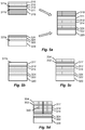
- Fig. 4a through 4d illustrate a further sequential integration process which is particularly suitable for a hetero-integration approach.
- Fig. 4a shows a wafer stack including a first wafer 210 and a second wafer 220.
- the layers/wafers 210, 212, 214, 216, 220, 222, 224, 226 forming part of the wafer stack corresponds to the layers/wafers 110, 112, 114, 116, 120, 122, 124, 126 of the wafer stack shown in Fig. 3a .
- the wafer stack including the first wafer 210 and the second wafer 220 may be formed in the manner described in connection with Fig. 3a .
- a first device region 212 is formed on a front side 210a of the first wafer 210.
- At least one interconnection layer 114 is formed on the first device region 112.
- a bonding layer 116 is formed on the interconnection layer 114.
- a device region 222, an interconnection layer 224 and a bonding layer 226 is formed on the front side 220a of the second wafer 120.
- the first wafer 210 is bonded to the second wafer 220 with the front side 210a of the first wafer 210 facing a front side 220a of the second wafer 220.
- a bonding layer 218 similar to bonding layers 216, 226 is formed on top of the wafer stack.
- Fig. 4a also shows a stack of layers including a bottom substrate 250 and a semiconductor layer 252.
- the semiconductor layer 252 is formed with a back side 252b facing the bottom substrate 250.
- a bonding layer 256 similar to the bonding layer 218 is formed on the front side 252a of the semiconductor layer 252.
- the bottom substrate 250 may include a Si-layer.
- a semiconductor layer 252 of a Ge-layer, a group III-V material layer may be grown on the Si-layer of the bottom substrate 250 in a conventional manner, with or without an intermediate SRB.
- the semiconductor layer 252 may also be formed as a layer stack including a Ge-layer epitaxially grown on the Si-layer of the bottom substrate 250, with or without an intermediate SRB, and a group III-V material layer epitaxially grown on the Ge-layer, with or without an intermediate SRB.
- the bottom substrate 250 may also be formed of a semiconductor material other than Si, for instance Ge, SiGe, SiC, GaAs or InP.
- the bottom substrate 250 may also be a SOI wafer, a GeOI wafer, SiGeOI wafer or a III-V-OI wafer.
- the bottom substrate 250 may alternatively function merely as a handling wafer and be formed of a dielectric material, such as a glass material.
- a device region (which may be referred to as a third device region) including a set of semiconductor devices may be formed on the front side 252a of the semiconductor layer 252.
- At least one interconnection layer for electrically interconnecting the semiconductor devices of the device region on the front side 252a may be formed on the device region.
- the optional presence of a device region and at least one interconnection layer is indicated by the dashed box 254 in Fig. 4a but will be omitted from the further discussion and figures for illustrational clarity.
- a wafer stack formed by bonding the stack including the bottom substrate 250 and the semiconductor layer 252 to a back side 210b of the first wafer 210 with the front side 252a of the semiconductor layer 252 facing the back side 210b of the first wafer 210.
- the bonding is achieved by the bonding layers 256, 218.
- the bottom substrate 250 has been removed to expose the back side 252b of the semiconductor layer 252.
- Removing the bottom substrate 250 may include grinding, CMP and/or etch back from the back side bottom substrate 250 until the semiconductor layer 252 is exposed (e.g. the Ge-layer or the SRB, if present).
- an optional thinning of the semiconductor layer 252 may be performed to form a thinned semiconductor layer 252'.
- the thinning may include grinding, CMP and/or etch back from the back side 252b of the semiconductor layer 252.
- a device region 232 (which may be referred to as a second device region of the first wafer 210 since the semiconductor layer 252 is bonded to the first wafer 210) is formed on the back side 252b of the semiconductor layer 252'.
- the device region 232 includes a set of semiconductor devices and defines a second FEOL layer of the first wafer 110.
- At least one interconnection layer 234 is formed on the device region 232.
- the at least one interconnection layer 234 forms a BEOL layer with respect to the device region 232.
- the device region 232 and the at least one interconnection layer 234 may be implemented in a similar manner as outlined in connection with the second device region 132 and the at least one interconnection layer 134 in Fig. 3b , respectively. Accordingly, preferably all FEOL processing steps relating to the device region 232, as well as BEOL processing steps relating to the at least one interconnection layer 234, are performed at temperatures below 600 °C or more preferably below 500 °C to avoid affecting BEOL layers and other FEOL layers already present in the wafer stack.
- a number of vias 240 is formed to extend through the wafer stack (by way of example four vias).
- the vias 240 may be formed with a similar structure and in a similar manner as the above described vias 140.
- the at least one interconnection layer 214 need not be present on the first device region 212. Furthermore, neither the device region 222 nor the at least one interconnection layer 224 are required to be present on the second wafer 220. Hence, in a basic variation of the above-described process device regions may be formed only on the front side 210a of the first wafer 210 and on the back side 252b of the semiconductor layer 252/252' (which is bonded to the back side 210b of the first wafer 210).
- the second wafer 220 may function as a handling wafer for the wafer stack and may accordingly be formed by a non-semiconductor material, for instance a dielectric material such as a glass material. Following formation of the vias 240, the second wafer 220 may be thinned or even removed.
- Fig. 5a through 5d illustrate a further sequential integration process which is particularly suitable for a hetero-integration approach.
- Fig. 5a shows a first wafer including a layer stack comprising a bottom substrate 310 and a semiconductor layer 311.
- the semiconductor layer 311 is formed with a back side 311 b facing the bottom substrate 310.
- a first device region 312 is formed on a front side 311 a of the semiconductor layer 311.
- the first device region 312 includes a set of semiconductor devices and defines a first FEOL layer of the first wafer.
- At least one interconnection layer 314 is formed on the first device region 312.
- a bonding layer 316 similar to any of the above-described bonding layers is formed on the at least one interconnection layer 314.
- the bottom substrate 310 may include a Si-layer.
- a semiconductor layer 311 of a Ge-layer, a group III-V material layer may be grown on the Si-layer of the bottom substrate 310 in a conventional manner, with or without an intermediate SRB.
- the semiconductor layer 311 may also be formed as a layer stack including a Ge-layer epitaxially grown on the Si-layer of the bottom substrate 310, with or without an intermediate SRB, and a group III-V material layer epitaxially grown on the Ge-layer, with or without an intermediate SRB.
- the bottom substrate 310 may also be formed of a semiconductor material other than Si, for instance Ge, SiGe, SiC, GaAs or InP.
- the bottom substrate 310 may also be a SOI wafer, a GeOI wafer, SiGeOI wafer or a III-V-OI wafer.
- the bottom substrate 310 may alternatively function merely as a handling wafer and be formed of a dielectric material, such as a glass material.
- Fig. 4a also shows a second wafer 320.
- the wafer/layers 320, 322, 324, 326 corresponds to the wafer/layers 120, 122, 124, 126 of the second wafer 120 shown in Fig. 3a .
- a wafer stack formed by bonding the semiconductor layer 311 of the first wafer to the second wafer 320 with the front side 311 a of the semiconductor layer 311 facing a front side 320a of the second wafer 320.
- the bonding is achieved by the bonding layers 316,326.
- the bottom substrate 310 of the first wafer has been removed to expose the back side 311 b of the semiconductor layer 311.
- Removing the bottom substrate 350 may include grinding, CMP and/or etch back from the back side bottom substrate 350 until the semiconductor layer 311 is exposed (e.g. the Ge-layer or the SRB, if present).
- an optional thinning of the semiconductor layer 311 may be performed to form a thinned semiconductor layer 311'.
- the thinning may include grinding, CMP and/or etch back from the back side 311 b of the semiconductor layer 311.
- a device region 332 (which may be referred to as a second device region of the first wafer) is formed on the back side 311 b of the semiconductor layer 311'.
- the device region 332 includes a set of semiconductor devices and defines a second FEOL layer of the first wafer.
- At least one interconnection layer 334 is formed on the device region 332.
- the at least one interconnection layer 334 forms a BEOL layer with respect to the device region 332.
- the device region 332 and the at least one interconnection layer 334 may be implemented in a similar manner as outlined in connection with the second device region 132 and the at least one interconnection layer 134 in Fig. 3b , respectively. Accordingly, preferably all FEOL processing steps relating to the device region 332, as well as BEOL processing steps relating to the at least one interconnection layer 334, are performed at temperatures below 600 °C or more preferably below 500 °C to avoid affecting BEOL layers and other FEOL layers already present in the wafer stack.
- a number of vias 340 is formed to extend through the wafer stack (by way of example three vias).
- the vias 340 may be formed with a similar structure and in a similar manner as the above described vias 140.
- the at least one interconnection layer 314 need not be present on the first device region 312. Furthermore, neither the device region 322 nor the at least one interconnection layer 324 are required to be present on the second wafer 320.
- device regions may be formed only on the front side 311 a of the semiconductor layer 311 of the first wafer and on the back side 311 b of the semiconductor layer 311/311'.
- the second wafer 320 may function as a handling wafer for the wafer stack and may accordingly be formed by a non-semiconductor material, for instance a dielectric material such as a glass material. Following formation of the vias 340, the second wafer 320 may be thinned or even removed.
Landscapes
- Internal Circuitry In Semiconductor Integrated Circuit Devices (AREA)
- Metal-Oxide And Bipolar Metal-Oxide Semiconductor Integrated Circuits (AREA)
Abstract
forming a wafer stack by bonding a first wafer (210) to a second wafer (220) with a front side of the first wafer facing a front side of the second wafer, the first wafer including a first device region (212) formed on the front side of the first wafer and including a set of semiconductor devices,
subsequent to forming the wafer stack, forming a second device region (232) on a back side of the first wafer, the second device region including a set of semiconductor devices,
forming at least one interconnection layer (234) on the second device region for electrically interconnecting the semiconductor devices of the second device region, and
forming at least one via (240) extending through the wafer stack from the at least one interconnection layer (234) and through the first wafer (210).
Description
- The present inventive concept relates to a sequential integration process.
- A conventional 3D integration process, also known as chip-stacking, involves stacking and bonding of two or more processed wafers on top of each other and interconnecting the devices of the processed wafers by vias. A prior art 3D integration process is schematically illustrated in
Fig. 1 wherein three processedwafers semiconductor device region 12, 22, 32 and aninterconnection layer 14, 24, 34, are stacked and bonded to each other via an oxide ornitride bonding layer - In a sequential or monolithic 3D integration process, the device processing is instead done subsequent to the wafer bonding. A prior art sequential 3D integration process is schematically illustrated in
Fig. 2 wherein asemiconductor substrate 50 is transferred on top of awafer 40 having asemiconductor device region 42, aninterconnection layer 44 and abonding layer 46. Processing for forming asemiconductor device region 52 on the front side of thesemiconductor substrate 50 is then performed. Aninterconnection layer 54 may be formed on thesemiconductor device region 52. Different levels of the stack may be connected by vias. - 3D integration processes allow forming of area efficient chips or integrated circuits. The sequential 3D integration process provides the additional benefit over the conventional integration process of enabling reduced device layer spacing and via height compared to the chip-stacking technique since the
wafer 40 supports thesubstrate 50 during the device processing on thesubstrate 50 and hence reduces the number of wafers needed. However there is still a need for further improvements in area efficiency. - An objective of the present inventive concept is to provide a sequential integration process enabling a further improvement in area efficiency of manufactured circuits compared to the prior art integration processes. Additional or alternative objectives may be understood from the following.
- According to an aspect of the present inventive concept there is provided a sequential integration process comprising:
- forming a wafer stack by bonding a first wafer to a second wafer with a front side of the first wafer facing a front side of the second wafer, the first wafer including a first device region formed on the front side of the first wafer and including a set of semiconductor devices,
- subsequent to forming the wafer stack, forming a second device region on a back side of the first wafer, the second device region including a set of semiconductor devices,
- forming at least one interconnection layer on the second device region for electrically interconnecting the semiconductor devices of the second device region, and
- forming at least one via extending through the wafer stack from the at least one interconnection layer and through the first wafer.
- By the inventive process an additional wafer surface namely the backside of the first wafer is made available for device integration. Accordingly a vertical wafer stack including a first wafer with both front and back side device regions may be formed. For a same number of wafers, this enables manufacturing of circuits of an improved area efficiency compared to the prior art processes.
- Since the second device region is formed after bonding of the first and the second wafer the inventive process may be referred to as a "sequential" integration process.
- As used herein, a "front side" and a "back side" of a wafer means opposite sides of the wafer, or in other words the sides formed by mutually opposite first and second main surfaces of the wafer.
- Forming or bonding a region/layer "on", or a region/layer being formed or bonded "to", a front/back side of a wafer may accordingly herein be understood as forming said region/layer, or said region/layer being formed or bonded, directly on the front/back side surface of the wafer (i.e. without any intermediate layers) or on the front/back side surface of the wafer with one or more intermediate layers between the front/back side surface of the wafer and the region/layer formed (i.e. the region/layer formed "at" the front/back side surface of the wafer).
- By a "device region" (e.g. the first or the second device region) is herein meant a region having a lateral or horizontal extension on a wafer or substrate side. A device region may also be referred to as an active device region. A device region of a wafer or substrate may form a front end of line (FEOL) device region of the wafer or substrate. A device region may include a set of planar or non-planar semiconductor devices, or a combination thereof.
- A thickness portion of a wafer or substrate, in which a device region is formed is formed, may be referred to as a device layer, an active device layer, or a FEOL (device) layer of the wafer / substrate.
- Dielectric regions may be formed in a semiconductor wafer or semiconductor substrate for device isolation. Dielectric regions may be formed by shallow-trench isolation (STI) regions. Dielectric regions may be formed before a device region has been formed, after a device region has been formed or between device region processing steps.
- The first device region may be formed by processing the front side of the first wafer to form the semiconductor devices in semiconductor material of the front side of the first wafer.
- The second device region may be formed by processing the back side of the first wafer to form the semiconductor devices in semiconductor material of the back side of the first wafer. Alternatively, the second device region may be formed by processing a semiconductor layer bonded to the back side of the first wafer to form the semiconductor devices in the semiconductor layer.
- The first device region and the second device region may include devices of different types. Devices may be formed of different semiconductor materials, include different combinations of dopants, and/or include different dopant concentrations.
- By at least one "interconnection layer" is herein meant one or more dielectric layers including conducting patterns or paths. A plurality of interconnection layers may be present including a plurality of interconnection levels (formed by conducting patterned layers) separated by inter-level dielectrics. Conductive paths of both inter- and intra-layer extension may be present. The conducting paths may electrically interconnect the semiconductor devices of a device region and optionally also interconnect contact regions (e.g. source, drain or gate) of individual semiconductor devices. The at least one interconnection layer may form middle end of line (MOL) and/or back end of line (BEOL) layers.
- By at least one "via" is herein meant at least one electrical connection extending in a vertical direction through the wafer stack.
- One or more of the vias may extend completely or at least partially through the first wafer.
- One or more of the vias may extend through a semiconductor portion of the first wafer and/or a dielectric/STI region of the first wafer (if such are present).
- One or more of the vias may form "inter-tier" vias. That is, the vias may interconnect device regions and/or interconnection layers at different "tiers" or "levels" of the wafer stack.
- One or more of the vias may form through substrate vias or through silicon vias (TSVs) with respect to at least the first wafer of the stack.
- One or more of the vias may extend from the at least one interconnection layer and at least to the first device region.
- One or more of the vias may electrically connect the at least one interconnection layer to one or more of the first device region and the second device region.
- Bonding of the first wafer to the second wafer (also generally applicable to any herein described bonding of a wafer, substrate or layer to another wafer, substrate or layer) may include bonding the first wafer and the second wafer via an intermediate bonding layer. A bonding layer may be formed on one or more of the wafer sides facing each other. A bonding layer may be an oxide layer wherein the wafers may be bonded by oxide-oxide bonding. A bonding layer may be a nitride layer wherein the wafers may be bonded by nitride-nitride bonding. Electrical insulation between wafers may thereby be achieved.
- According to one embodiment the method further comprises bonding a semiconductor layer to the back side of the first wafer with a front side of said semiconductor layer facing the back side of the first wafer, wherein the forming of the second device region includes forming the second device region on a back side of said semiconductor layer.
- The second device region may accordingly be formed on the backside of the first wafer with at least a thickness portion of a semiconductor layer intermediate the first wafer and the second device region.
- By forming the second device region on the backside of a semiconductor layer, hetero-integration is enabled, i.e. integration of different material systems in the wafer stack.
- The at least one interconnection layer formed on the second device region of the semiconductor layer may form MOL and/or BEOL layers of the semiconductor layer, i.e. with respect to the second device region.
- One or more of the vias may extend from the at least one interconnection layer, through the semiconductor layer and the first wafer. One or more of the vias may extend to the first device region of the first wafer and optionally also to an interconnection layer formed on the first device region of the first wafer (if such a layer is present).
- One or more of the vias may electrically connect the at least one interconnection layer formed on the second device region to one of more of the first device region, an interconnection layer formed on the first device region and the second device region.
- The semiconductor material forming the semiconductor devices of the second device region may be different from a semiconductor material forming the semiconductor devices of the first device region. Advantageously the first device region includes Si semiconductor devices and the second device region includes Ge or group III-V semiconductor material devices, or vice versa.
- Different device technology may be implemented in the first device region and the second device region, for instance a combination of analog devices and digital devices, combinations of I/O devices, radio frequency (RF) devices and/or ESD devices (i.e. devices for protection from electrostatic discharge). It is also possible to form planar transistors in one of the device regions and non-planar transistors (e.g. FinFETs or nanowire transistors) in the other device region. It is also possible to form devices in the device regions using different process technology nodes, for instance the N45 node in one of the device regions and the N14 node in the other device region. Using slower nodes for implementing devices / circuitry for slower applications may reduce overall costs.
- The semiconductor layer (which also may be referred to as a semiconductor substrate) may be formed on a bottom substrate. Subsequent to the bonding of the semiconductor layer to the first wafer, the bottom substrate may be removed from said semiconductor layer to expose the back side of the semiconductor layer and thereafter the second device region may be formed on the back side of said semiconductor layer. The bottom substrate may thereby function as a handling or donor wafer for the semiconductor layer and thus facilitate transfer of a comparably thin semiconductor layer to the wafer stack.
- The act of forming the semiconductor layer on the bottom substrate may form part of the inventive process, or a semiconductor layer may be formed on a bottom substrate in a process separate from the inventive process and provided as pre-made component to the inventive process.
- Subsequent to removing the bottom substrate, and prior to forming the second device region, thinning of the semiconductor layer may be performed.
- By thinning the semiconductor substrate prior to forming of the second device region the height of the final stack may be reduced and any defective portions of the semiconductor layer may be removed. Also, an appropriate layer thickness for the intended device type may be obtained.
- The bottom substrate may include a Si-layer and the semiconductor layer may be formed by a group IV material layer. The group IV material layer may be formed by Ge, SiGe, SiC, or GeSn. A group IV material layer (i.e. other than Si) may be grown on the Si bottom substrate with or without an intermediate strain relaxed buffer (SRB).
- The bottom substrate may include a Si-layer and the semiconductor layer may be formed by a group III-V material layer or by a stack including a group III-V material layer formed on a Ge-layer.
- The group III-V material layer may be formed by AlAs, GaN, AlGaN, InN, AlN, GaP, GaAs, InP, InAs, InGaAs, InAlAs, InGaP, InSb, AlSb or InGaSb.
- A Ge-layer may be grown on a Si bottom substrate with or without an intermediate SRB. A group III-V material layer may grown on a Ge-layer with or without an intermediate SRB.
- A group III-V material layer enables forming of semiconductor devices with increased cut-off frequency compared to group IV materials. A group III-V material layer thus lends itself favorably to supporting a device region implementing RF devices. A group III-V material layer also offers improved electron mobility compared to group IV materials. A group III-V material layer thus lends itself favorably also to supporting a device region implementing NMOS devices.
- Forming the semiconductor layer as a stack of a Ge-layer and a group III-V material layer enables device regions including Ge- and group III-V semiconductor devices to be formed on opposite sides of the semiconductor layer. The device region on the Ge-layer may include PMOS devices (Ge presents advantageous hole mobility). The device region on the group III-V material layer may include NMOS devices (III-V materials present advantageous electron mobility).
- In addition to the second device region, also a third device region including a set of semiconductor devices may be formed on the front side of said semiconductor layer. The third device region may be formed prior to the bonding of said semiconductor layer to the first wafer.
- The act of forming the third device region may form part of the inventive process, or a third device region may be formed on the front side of the semiconductor layer in a process separate from the inventive process wherein a semiconductor substrate with a front side device region may be provided as a pre-made component to the process.
- The second and the third device region may form two mutually opposite FEOL device regions / layers of the semiconductor layer.
- The third device region may include a set of planar or non-planar semiconductor devices, or a combination thereof.
- The second device region and the third device region may include devices of different types. Devices may include different combinations of dopants, and/or include different dopant concentrations. The devices may be formed using different process technology nodes.
- At least one interconnection layer may be formed on the third device region for electrically interconnecting the semiconductor devices of the third device region.
- The at least one interconnection layer may form MOL and/or BEOL layers of the semiconductor substrate, i.e. with respect to the third device region.
- The act of forming the at least one interconnection layer on the third device region may form part of the inventive process, or at least one interconnection layer may be formed on the third device region of the semiconductor layer in a process separate from the inventive process wherein a semiconductor substrate with a front side device region and an interconnection layer may be provided as a pre-made component to the inventive process.
- According to embodiments wherein the second device region is formed on the back side of the semiconductor layer the first wafer may be formed of a semiconductor material, for instance Si, Ge, SiGe, SiC, GaAs or InP. The first wafer may also be a SOI wafer, a GeOI wafer, SiGeOI wafer or a III-V-OI wafer. The second wafer may be formed of a semiconductor material, for instance Si, Ge, SiGe, SiC, GaAs, InP. The second wafer may also be a SOI wafer, a GeOI wafer, SiGeOI wafer, or a III-V-OI wafer. The second wafer may also be formed of a non-semiconductor material such as a dielectric material, advantageously a glass material.
- According to embodiments wherein the second wafer is formed of a semiconductor material a device region including a set of semiconductor devices may be formed on the front side of the second wafer. It is hence possible to obtain a wafer stack wherein as many as four different device regions are formed on different levels of the stack of the second wafer/first wafer/semiconductor substrate, i.e. on the front side of the second wafer, on the front side of the first wafer, on the front side of the semiconductor layer and on the backside of the semiconductor layer.
- At least one interconnection layer may be formed on the device region of the second wafer for electrically interconnecting the semiconductor devices of the device region of the second wafer. The forming of the at least one interconnection layer may be performed prior to the bonding of the first wafer to the second wafer.
- The at least one interconnection layer may form MOL and/or BEOL layers of the second wafer, i.e. with respect to the device region formed on the second wafer.
- The act of forming a device region on the front side of the second wafer and/or the act of forming the at least one interconnection layer on the device region of the second wafer may form part of the inventive process, or a device region and/or at least one interconnection layer may be formed on the second wafer in a process separate from the inventive process wherein a second wafer with a front side device region and optionally also an interconnection layer may be provided as a pre-made component to the process.
- One or more of the vias may extend from the at least one interconnection layer formed on the second device region, through the semiconductor layer, the first wafer and to the device region of the second wafer or at least to an interconnection layer formed on the device region of the second wafer (if such a layer is present).
- One or more of the vias may electrically connect the at least one interconnection layer formed on the second device region to one of more of the first device region, an interconnection layer formed on the first device region, the second device region, the device region formed on the second wafer, and an interconnection layer formed on the device region of the second wafer (if such a layer is present).
- According to embodiments wherein the second wafer is formed of a non-semiconductor material the second wafer may serve as a handling wafer and facilitate handling of the wafer stack during the process. The second wafer may be removed or thinned subsequent to forming of the interconnection layer on the second device region of the semiconductor layer. Removing or thinning of the second wafer may include grinding, CMP and/or etch back from the backside of the second wafer.
- According to one embodiment the first wafer includes a semiconductor layer, wherein the first device region is formed on a front side of said semiconductor layer and bonding the first wafer to the second wafer includes bonding the front side of the semiconductor layer to the second wafer, and the method further comprises, subsequent to said bonding to the second wafer, forming the second device region on a back side of said semiconductor layer.
- The second device region may accordingly be formed directly on the backside of the first wafer, the backside being formed by the semiconductor layer.
- By forming the second device region on the backside of a semiconductor layer, hetero-integration is enabled, i.e. integration of different material systems in the stack.
- The first and the second device region may form two mutually opposite FEOL device regions / layers of the semiconductor layer.
- At least one interconnection layer may be formed on the first device region for electrically interconnecting the semiconductor devices of the first device region.
- The at least one interconnection layer may form MOL and/or BEOL layers of the semiconductor layer, i.e. with respect to the first device region.
- The act of forming the at least one interconnection layer on the first device region may form part of the inventive process, or at least one interconnection layer may be formed on the first device region of the semiconductor layer in a process separate from the inventive process wherein a first wafer with a front side device region and an interconnection layer may be provided as a pre-made component to the process.
- According to embodiments wherein the second device region is formed on the back side of the semiconductor layer of the first wafer, the second wafer may be formed of a semiconductor material, for instance Si, Ge, SiGe, SiC, GaAs, InP. The second wafer may also be a SOI wafer, a GeOI wafer, SiGeOI wafer, or a III-V-OI wafer. The second wafer may also be formed of a non-semiconductor material such as a dielectric material, advantageously a glass material.
- According to embodiments wherein the second wafer is formed of a semiconductor material a device region including a set of semiconductor devices may be formed on the front side of the second wafer.
- It is hence possible to obtain a wafer stack wherein as many as three different device regions are formed on different levels of the stack of the second wafer/first wafer, i.e. on the front side of the second wafer, on the front side of the semiconductor layer and on the backside of the semiconductor layer.
- The device region of the second wafer may include a set of planar or non-planar semiconductor devices, or a combination thereof.
- The device region of the second wafer may include devices of types different from the first and second device regions of the semiconductor layer. Devices may be formed of different semiconductor materials, include different combinations of dopants, and/or include different dopant concentrations. The devices may be formed using different process technology nodes.
- At least one interconnection layer may be formed on the device region of the second wafer for electrically interconnecting the semiconductor devices of the device region of the second wafer. The forming of the at least one interconnection layer may be performed prior to the bonding of the first wafer to the second wafer.
- The at least one interconnection layer may form MOL and/or BEOL layers of the second wafer, i.e. with respect to the device region formed on the second wafer.
- The act of forming a device region on the front side of the second wafer and/or the act of forming the at least one interconnection layer on the device region of the second wafer may form part of the inventive process, or a device region and/or at least one interconnection layer may be formed on the second wafer in a process separate from the inventive process wherein a second wafer with a front side device region and optionally also an interconnection layer may be provided as a pre-made component to the process.
- The semiconductor material forming the semiconductor devices of the first and the second device region of the first wafer may be formed by a semiconductor material which is different from a semiconductor material forming the semiconductor devices of the device region of the second wafer. Accordingly different device technology may be implemented in the first/second device region of the semiconductor layer/first wafer and the device region of the second wafer, for instance a combination of analog devices and digital devices, combinations of I/O devices, RF devices and/or ESD devices. It is also possible to form planar transistors in at least one of the device regions and non-planar transistors (e.g. FinFETs or nanowire transistors) in at least one of the other device region(s). It is also possible to form devices in the device regions using different process technology nodes, for instance the N45 node in at least one of the device regions and the N14 node in at least one of the other device region(s). Using slower nodes for implementing devices / circuitry for slower applications may reduce overall costs.
- The first wafer may further include a bottom substrate, the back side of the semiconductor layer facing the bottom substrate, wherein the method may further comprise, subsequent to said bonding to the second wafer, removing the bottom substrate from said semiconductor layer to expose the back side of the semiconductor layer and thereafter forming the second device region on the back side of said semiconductor layer.
- The bottom substrate may include a Si-layer and the semiconductor layer may be formed by a group IV material layer. The group IV material layer may be formed by Ge, SiGe, SiC, or GeSn. A group IV material layer (i.e. other than Si) may be grown on the Si bottom substrate with or without an intermediate SRB.
- The bottom substrate may include a Si-layer and the semiconductor layer may be formed by a group III-V material layer or by a stack including a group III-V material layer formed on a Ge-layer.
- The group III-V material layer may be formed by AlAs, GaN, AlGaN, InN, AIN, GaP, GaAs, InP, InAs, InGaAs, InAlAs, InGaP, InSb, AlSb or InGaSb.
- A Ge-layer may be grown on a Si bottom substrate with or without an intermediate SRB. A group III-V material layer may grown on a Ge-layer with or without an intermediate SRB.
- A group III-V material layer enables forming of semiconductor devices with increased cut-off frequency compared to group IV materials. A group III-V material layer thus lends itself favorably to supporting a device region implementing RF devices. A group III-V material layer also offers improved electron mobility compared to group IV materials. A group III-V material layer thus lends itself favorably also to supporting a device region implementing NMOS devices.
- Forming the semiconductor layer as a stack of a Ge-layer and a group III-V material layer enables device regions including Ge- and group III-V semiconductor devices to be formed on opposite sides of the semiconductor layer. The device region on the Ge-layer may include PMOS devices (Ge presents advantageous hole mobility). The device region on the group III-V material layer may include NMOS devices (III-V materials present advantageous electron mobility).
- One or more of the vias may extend from the at least one interconnection layer formed on the second device region, through the semiconductor layer of the first wafer, and to the device region of the second wafer or at least to an interconnection layer formed on the device region of the second wafer (if such a layer is present).
- One or more of the vias may electrically connect the at least one interconnection layer formed on the second device region to one of more of the first device region, an interconnection layer formed on the first device region, the second device region, the device region formed on the second wafer, and an interconnection layer formed on the device region of the second wafer (if such a layer is present).
- According to one embodiment the forming of the second device region includes forming the second device region directly on the back side of the first wafer. Hence no separate dedicated handling wafer for supporting a layer / substrate implementing the second device region is required.
- This embodiment advantageously lends itself for homo-integration since a same wafer, i.e. the first wafer, implements both the first and the second device region.
- The first and the second device region may form two mutually opposite FEOL device regions / layers of the first wafer.
- Subsequent to bonding the first wafer to the second wafer, and prior to forming the second device region, thinning of the first wafer may be performed wherein the second device region may be formed on the back side of the thinned first wafer. Thinning of the first wafer may include performing a CMP on the backside of the first wafer. By thinning the semiconductor substrate prior to forming of the second device region the height of the final stack may be reduced and any defective portions of the semiconductor layer may be removed.
- The first wafer may be formed of a semiconductor material, for instance Si, Ge, SiGe, SiC, GaAs, InP. The first wafer may also be a SOI wafer, a GeOI wafer, SiGeOI wafer or a III-V-OI wafer. The second wafer may be formed of a semiconductor material, for instance Si, Ge, SiGe, SiC, GaAs, InP. The second wafer may also be a SOI wafer, a GeOI wafer, SiGeOI wafer, or a III-V-OI wafer. The second wafer may also be formed of a non-semiconductor material such as a dielectric material, advantageously a glass material.
- According to embodiments wherein the second wafer is formed of a semiconductor material a device region including a set of semiconductor devices may be formed on the front side of the second wafer.
- It is hence possible to obtain a wafer stack wherein as many as three different device regions are formed on different levels of the stack of the second wafer/first wafer, i.e. on the front side of the second wafer, on the front side of the first wafer and on the backside of the first wafer.
- The device region of the second wafer may include a set of planar or non-planar semiconductor devices, or a combination thereof.
- The device region of the second wafer may include devices of types different from the first and second device regions of the semiconductor layer. Devices may be formed of different semiconductor materials, include different combinations of dopants, and/or include different dopant concentrations. The devices may be formed using different process technology nodes.
- At least one interconnection layer may be formed on the device region of the second wafer for electrically interconnecting the semiconductor devices of the device region of the second wafer. The forming of the at least one interconnection layer may be performed prior to the bonding of the first wafer to the second wafer.
- The at least one interconnection layer may form MOL and/or BEOL layers of the second wafer, i.e. with respect to the device region formed on the second wafer.
- The act of forming a device region on the front side of the second wafer and/or the act of forming the at least one interconnection layer on the device region of the second wafer may form part of the inventive process, or a device region and/or at least one interconnection layer may be formed on the second wafer in a process separate from the inventive process wherein a second wafer with a front side device region and optionally also an interconnection layer may be provided as a pre-made component to the process.
- The semiconductor material forming the semiconductor devices of the first and the second device region of the first wafer may be formed by a semiconductor material which is different from a semiconductor material forming the semiconductor devices of the device region of the second wafer. Accordingly different device technology may be implemented in the first/second device region of the first wafer and the device region of the second wafer, for instance a combination of analog devices and digital devices, combinations of I/O devices, RF devices and/or ESD devices. It is also possible to form planar transistors in at least one of the device regions and non-planar transistors (e.g. FinFETs or nanowire transistors) in at least one of the other device region(s). It is also possible to form devices in the device regions using different process technology nodes, for instance the N45 node in at least one of the device regions and the N14 node in at least one of the other device region(s). Using slower nodes for implementing devices / circuitry for slower applications may reduce overall costs.
- One or more of the vias may extend from the at least one interconnection layer formed on the second device region, through the first wafer, and to the device region of the second wafer or at least to an interconnection layer formed on the device region of the second wafer (if such a layer is present).
- One or more of the vias may electrically connect the at least one interconnection layer formed on the second device region to one of more of the first device region, an interconnection layer formed on the first device region, the second device region, the device region formed on the second wafer, and an interconnection layer formed on the device region of the second wafer.
- According to another aspect there is provided a wafer stack including a first wafer and a second wafer, the first wafer being bonded to the second wafer with a front side of the first wafer facing a front side of the second wafer, wherein the first wafer includes:
- a first device region formed on the front side of the first wafer and including a set of semiconductor devices,
- a second device region formed on a back side of the first wafer and including a set of semiconductor devices, and
- at least one interconnection layer arranged on the second device region for electrically interconnecting the semiconductor devices of the second device region,
- the wafer stack further including at least one via extending through the wafer stack from the at least one interconnection layer and through the first wafer.
- The various advantages and variations of the wafer stack, as well as details thereof, discussed in the above apply corresponding to the wafer stack aspect. Reference is therefore made to the above discussion.
- The above, as well as additional objects, features and advantages of the present inventive concept, will be better understood through the following illustrative and non-limiting detailed description of preferred embodiments of the present inventive concept, with reference to the appended drawings. In the drawings like reference numerals will be used for like elements unless stated otherwise.
-
Fig. 1 and 2 are schematic illustrations of prior art 3D integration processes. -
Fig. 3 ,4 and5 are schematic illustrations of different sequential integration processes. - A number of sequential integration processes will now be described with reference to
Figures 3 to 5 . In the figures, various wafer stacks are schematically shown in a cross-section taken vertically through the stacks. Only portions of the layers forming part of the stacks are shown and the layers may extend laterally / horizontally beyond the illustrated portions. It should also be noted that for the purpose of clarity the various layers and other features of the stacks are not drawn to scale and their relative dimensions, in particular their thickness, may differ from a physical stack. -
Fig. 3a through 3c illustrate a sequential integration process which is particularly suitable for a homo-integration approach. -
Fig. 3a shows afirst wafer 110. Thefirst wafer 110 may be of a semiconductor material such as Si, Ge, SiGe, SiC, GaAs or InP. Thefirst wafer 110 may also be a SOI wafer, a GeOI wafer, SiGeOI wafer or a III-V-OI wafer. Afirst device region 112 is formed on afront side 110a of thefirst wafer 110. At least oneinterconnection layer 114 is formed on thefirst device region 112. Abonding layer 116 is formed on theinterconnection layer 114. - The
first device region 112 includes a set of semiconductor devices and defines a first FEOL layer of thefirst wafer 110. The set of semiconductor devices may include planar or non-planar devices. By way of example, the set of semiconductor devices may include metal-oxide-semiconductor field-effect transistors (MOSFETs), metal-insulator-semiconductor field-effect transistors (MISFETs), bipolar transistors (BJTs), heterojunction BJTs (HBTs), fin field-effect transistors (FinFETs), nanowire FETs, high electron mobility transistors (HEMT), junction less transistor (JLT), tunnel Field effect transistor (TFET). The semiconductor devices may be formed using conventional device fabrication / FEOL processing in accordance with the particular type of devices. - Although in the drawings, the device regions are generally illustrated as layers it is noted that a device region typically may present a limited horizontal extension on a wafer side. Semiconductor devices need hence not be present throughout the layers indicated in the drawings. However, the designation "device/FEOL layer" may be understood to refer to a thickness portion of a wafer/substrate in or on which a device region (for instance the first device region 112) is formed.
- By way of example, FEOL processing for forming a set of planar FETs may include a number of different processing stages or module including for instance forming of device isolation using the shallow trench isolation (STI) technique on the front side of the
first wafer 110. Forming of STI regions may be followed by formation of the gate which could be formed by either a gate first or a gate last process (also known as replacement metal gate process). In a gate first process the gate dielectric and the gate conductor are formed prior to forming of source and drain regions. In a gate last process the final gate dielectric and gate conductor are formed after forming of source and drain regions. In an example gate last process a dummy gate oxide and a dummy gate (e.g. of amorphous/poly Si) may be deposited and patterned. Source and drain region may then be formed by implantation and subsequent annealing or by in-situ epitaxial growth of a doped semiconductor layer. An interlayer dielectric (ILD) deposition may thereafter be performed. Following CMP of the ILD, the dummy gate and dummy gate oxide may be removed to create a trench in the ILD. A gate dielectric and a gate conductor may be deposited to fill the trench. Portions of the gate conductor deposited outside the trench may be removed by CMP. Contact windows may be opened above the source and drain regions and filled with metal. In the gate last process spacers may be formed on the dummy gate or the final gate by spacer material deposition. - The above discussion concerning the
first device region 112 and the FEOL processing is applicable also to the further device regions discussed below. The discussion will therefore not be repeated in connection with the further device regions. - The at least one
interconnection layer 114 is formed on thefirst device region 112 for interconnecting the semiconductor devices of thefirst device region 112. The at least oneinterconnection layer 114 forms a BEOL layer with respect to thefirst device region 112. The at least oneinterconnection layer 114 may include a plurality of dielectric layers including conductive paths. The conductive paths may be formed by a conductive material, for instance metallic conductors such as Cu, W, Au, Ag, Al, Co or Ru. The dielectric layers may be formed for instance by silicon oxide, silicon oxide nitride, silicon carbide nitride or silicon nitride. - Also shown in
Fig. 3a is asecond wafer 120. Similar to thefirst wafer 110, adevice region 122, aninterconnection layer 124 and abonding layer 126 is formed on afront side 120a of thesecond wafer 120. Thefirst wafer 120 and thesecond wafer 120 may be formed of a material of a same or a different type. Thedevice region 122 and theinterconnection layer 124 may be formed to implement desired type(s) of devices and circuitry. - At the right-hand side of
Fig. 3a is shown a wafer stack formed by bonding thefirst wafer 110 to thesecond wafer 120 with thefront side 110a of thefirst wafer 110 facing thefront side 120a of thesecond wafer 120. As seen inFig. 3a aback side 110b of thefirst wafer 110 thereby forms a front side of the wafer stack. - The bonding is achieved by the bonding layers 116, 126. The bonding layers 116, 126 may be oxide or nitride layers wherein the
wafers wafers wafers - In
Fig. 3b , asecond device region 132 is formed on theback side 110b of thefirst wafer 110. Thesecond device region 132 includes a set of semiconductor devices and defines a second FEOL layer of thefirst wafer 110. At least oneinterconnection layer 134 is formed on thesecond device region 132. The at least oneinterconnection layer 134 forms a BEOL layer with respect to thesecond device region 132. - The
second device region 132 and the at least oneinterconnection layer 134 may be implemented in a similar manner as outlined in connection with thefirst device region 112 and the at least oneinterconnection layer 114, respectively. However it should be noted that, preferably, all FEOL processing steps to form thesecond device region 132, as well as BEOL processing steps to form the at least oneinterconnection layer 134, are performed at temperatures below 600 °C or more preferably below 500 °C to avoid affecting BEOL layers and other FEOL layers already present in the wafer stack. More generally, the limit on temperature could vary depending upon metal and type of inter metal dielectric used in the BEOL layer and time for which the wafer stack is subjected to these temperature. - As shown in
Fig. 3b , prior to forming thesecond device region 132, an optional thinning of thefirst wafer 110 may be performed. The thinning may include grinding and/or (selective) etch back from theback side 110b of thefirst wafer 110, optionally followed by CMP. Thesecond device region 132 may thereafter be formed on the thinned wafer 110'. - In
Fig. 3c a number ofvias 140 is formed to extend through the wafer stack. AlthoughFig. 3c shows fourvias 140 this only represents an example and the number ofvias 140 will be implementation specific. By way of example, two vias extend from the at least oneinterconnection layer 134, through the first wafer 110', the at least oneinterconnection layer 114 and the bonding layers to the at least oneinterconnection layer 124. Said two vias may accordingly electrically interconnect the at least one interconnection layers 134, 114 and 124 and thedevice regions interconnection layer 134, through first wafer 110' to the at least oneinterconnection layer 114. Said other two vias may accordingly electrically interconnect the at least one interconnection layers 134 and 114 and thedevice regions - The
vias 140 may be formed by a conductive material, for instance metallic conductors such as Cu, W, Au, Ag, Al, Co, Ni, Ru or by highly doped semiconductor material. Thevias 140 may further include a liner material formed by a dielectric material, such as a silicon oxide or silicon nitride. Vias formed by conductive material and dielectric liner may be referred to as TSVs. extending through semiconductor material regions Vias extending only through dielectric material, such as STI regions, need not be formed with a dielectric liner and may be referred to as inter-tier vias. - The
vias 140 may be formed in a conventional manner, by forming a respective trench through the wafer stack at the intended positions of thevias 140 to be formed. An etch mask (not shown) may be formed above the at least oneinterconnection layer 134 with openings defining the positions of the trenches. The mask may be patterned using lithography and etching. The trenches may be formed by anisotropic etching through the mask openings. The etching may be continued until trenches with a desired depth have been formed, typically at a depth corresponding to one of the interconnection layers 114 or 124. A via liner material may be deposited in the trenches and subsequently a conductive material may be deposited in the trenches. The liner may function as an insulator to prevent a short between the conductive material and semiconductor layer or it could function as a diffusion barrier along sections not extending through semiconductor material. The mask may be stripped and any material deposited outside the trenches may be removed by CMP. Masking material as well as lithography and etching technique may be selected in accordance with the material systems and device implementation of thefirst wafer 110. Ifvias 140 of different materials or dimensions (e.g. height or depth) are to be formed the forming thevias 140 may be formed by repeating the above process steps a number of times to form each desired via structure. - Following forming of the structure shown in
Fig. 3c further back end or packaging processing may be performed in a conventional manner, including for instance forming of contact pads above the at least oneinterconnection layer 134 to provide a contact interface towards thevias 140. - In a variation of the process described with reference to
Fig. 3a-c the at least oneinterconnection layer 114 need not be present on thefirst device region 112. Furthermore, neither thedevice region 122 nor the at least oneinterconnection layer 124 are required to be present on thesecond wafer 120. Hence, in a basic variation of the above-described process device regions may be formed only on thefront side 110a and theback side 110b of thefirst wafer 110/110'. In that case, thesecond wafer 120 may function as a handling wafer for the wafer stack and may accordingly be formed by a non-semiconductor material, for instance a dielectric material such as a glass material. Following formation of thevias 140, thesecond wafer 120 may be thinned or even removed. -
Fig. 4a through 4d illustrate a further sequential integration process which is particularly suitable for a hetero-integration approach. -
Fig. 4a shows a wafer stack including afirst wafer 210 and asecond wafer 220. The layers/wafers wafers Fig. 3a . The wafer stack including thefirst wafer 210 and thesecond wafer 220 may be formed in the manner described in connection withFig. 3a . - Accordingly, a
first device region 212 is formed on afront side 210a of thefirst wafer 210. At least oneinterconnection layer 114 is formed on thefirst device region 112. Abonding layer 116 is formed on theinterconnection layer 114. Similar to thefirst wafer 210, adevice region 222, aninterconnection layer 224 and abonding layer 226 is formed on thefront side 220a of thesecond wafer 120. Thefirst wafer 210 is bonded to thesecond wafer 220 with thefront side 210a of thefirst wafer 210 facing afront side 220a of thesecond wafer 220. Abonding layer 218 similar tobonding layers -
Fig. 4a also shows a stack of layers including abottom substrate 250 and asemiconductor layer 252. Thesemiconductor layer 252 is formed with aback side 252b facing thebottom substrate 250. Abonding layer 256 similar to thebonding layer 218 is formed on thefront side 252a of thesemiconductor layer 252. - The
bottom substrate 250 may include a Si-layer. Asemiconductor layer 252 of a Ge-layer, a group III-V material layer may be grown on the Si-layer of thebottom substrate 250 in a conventional manner, with or without an intermediate SRB. Thesemiconductor layer 252 may also be formed as a layer stack including a Ge-layer epitaxially grown on the Si-layer of thebottom substrate 250, with or without an intermediate SRB, and a group III-V material layer epitaxially grown on the Ge-layer, with or without an intermediate SRB. Thebottom substrate 250 may also be formed of a semiconductor material other than Si, for instance Ge, SiGe, SiC, GaAs or InP. Thebottom substrate 250 may also be a SOI wafer, a GeOI wafer, SiGeOI wafer or a III-V-OI wafer. Thebottom substrate 250 may alternatively function merely as a handling wafer and be formed of a dielectric material, such as a glass material. - Optionally, a device region (which may be referred to as a third device region) including a set of semiconductor devices may be formed on the
front side 252a of thesemiconductor layer 252. At least one interconnection layer for electrically interconnecting the semiconductor devices of the device region on thefront side 252a may be formed on the device region. The optional presence of a device region and at least one interconnection layer is indicated by the dashedbox 254 inFig. 4a but will be omitted from the further discussion and figures for illustrational clarity. - At the right-hand side of
Fig. 4a is shown a wafer stack formed by bonding the stack including thebottom substrate 250 and thesemiconductor layer 252 to aback side 210b of thefirst wafer 210 with thefront side 252a of thesemiconductor layer 252 facing theback side 210b of thefirst wafer 210. The bonding is achieved by the bonding layers 256, 218. - In
Fig. 4b , thebottom substrate 250 has been removed to expose theback side 252b of thesemiconductor layer 252. Removing thebottom substrate 250 may include grinding, CMP and/or etch back from the backside bottom substrate 250 until thesemiconductor layer 252 is exposed (e.g. the Ge-layer or the SRB, if present). - As shown in
Fig. 4b , an optional thinning of thesemiconductor layer 252 may be performed to form a thinned semiconductor layer 252'. The thinning may include grinding, CMP and/or etch back from theback side 252b of thesemiconductor layer 252. - In
Fig. 4c , a device region 232 (which may be referred to as a second device region of thefirst wafer 210 since thesemiconductor layer 252 is bonded to the first wafer 210) is formed on theback side 252b of the semiconductor layer 252'. Thedevice region 232 includes a set of semiconductor devices and defines a second FEOL layer of thefirst wafer 110. At least oneinterconnection layer 234 is formed on thedevice region 232. The at least oneinterconnection layer 234 forms a BEOL layer with respect to thedevice region 232. - The
device region 232 and the at least oneinterconnection layer 234 may be implemented in a similar manner as outlined in connection with thesecond device region 132 and the at least oneinterconnection layer 134 inFig. 3b , respectively. Accordingly, preferably all FEOL processing steps relating to thedevice region 232, as well as BEOL processing steps relating to the at least oneinterconnection layer 234, are performed at temperatures below 600 °C or more preferably below 500 °C to avoid affecting BEOL layers and other FEOL layers already present in the wafer stack. - In
Fig. 4d a number ofvias 240 is formed to extend through the wafer stack (by way of example four vias). Thevias 240 may be formed with a similar structure and in a similar manner as the above describedvias 140. - Following forming of the structure shown in
Fig. 4d further back end processing may be performed as described in connection withFig. 3c . - In a variation of the process described with reference to
Fig. 4a-d the at least oneinterconnection layer 214 need not be present on thefirst device region 212. Furthermore, neither thedevice region 222 nor the at least oneinterconnection layer 224 are required to be present on thesecond wafer 220. Hence, in a basic variation of the above-described process device regions may be formed only on thefront side 210a of thefirst wafer 210 and on theback side 252b of thesemiconductor layer 252/252' (which is bonded to theback side 210b of the first wafer 210). In that case, thesecond wafer 220 may function as a handling wafer for the wafer stack and may accordingly be formed by a non-semiconductor material, for instance a dielectric material such as a glass material. Following formation of thevias 240, thesecond wafer 220 may be thinned or even removed. -
Fig. 5a through 5d illustrate a further sequential integration process which is particularly suitable for a hetero-integration approach. -
Fig. 5a shows a first wafer including a layer stack comprising abottom substrate 310 and asemiconductor layer 311. Thesemiconductor layer 311 is formed with aback side 311 b facing thebottom substrate 310. Afirst device region 312 is formed on afront side 311 a of thesemiconductor layer 311. Thefirst device region 312 includes a set of semiconductor devices and defines a first FEOL layer of the first wafer. At least oneinterconnection layer 314 is formed on thefirst device region 312. Abonding layer 316 similar to any of the above-described bonding layers is formed on the at least oneinterconnection layer 314. - The
bottom substrate 310 may include a Si-layer. Asemiconductor layer 311 of a Ge-layer, a group III-V material layer may be grown on the Si-layer of thebottom substrate 310 in a conventional manner, with or without an intermediate SRB. Thesemiconductor layer 311 may also be formed as a layer stack including a Ge-layer epitaxially grown on the Si-layer of thebottom substrate 310, with or without an intermediate SRB, and a group III-V material layer epitaxially grown on the Ge-layer, with or without an intermediate SRB. Thebottom substrate 310 may also be formed of a semiconductor material other than Si, for instance Ge, SiGe, SiC, GaAs or InP. Thebottom substrate 310 may also be a SOI wafer, a GeOI wafer, SiGeOI wafer or a III-V-OI wafer. Thebottom substrate 310 may alternatively function merely as a handling wafer and be formed of a dielectric material, such as a glass material. -
Fig. 4a also shows asecond wafer 320. The wafer/layers layers second wafer 120 shown inFig. 3a . - At the right-hand side of
Fig. 5a is shown a wafer stack formed by bonding thesemiconductor layer 311 of the first wafer to thesecond wafer 320 with thefront side 311 a of thesemiconductor layer 311 facing afront side 320a of thesecond wafer 320. The bonding is achieved by the bonding layers 316,326. - In
Fig. 5b , thebottom substrate 310 of the first wafer has been removed to expose theback side 311 b of thesemiconductor layer 311. Removing the bottom substrate 350 may include grinding, CMP and/or etch back from the back side bottom substrate 350 until thesemiconductor layer 311 is exposed (e.g. the Ge-layer or the SRB, if present). - As shown in
Fig. 5b , an optional thinning of thesemiconductor layer 311 may be performed to form a thinned semiconductor layer 311'. The thinning may include grinding, CMP and/or etch back from theback side 311 b of thesemiconductor layer 311. - In
Fig. 5c , a device region 332 (which may be referred to as a second device region of the first wafer) is formed on theback side 311 b of the semiconductor layer 311'. Thedevice region 332 includes a set of semiconductor devices and defines a second FEOL layer of the first wafer. At least oneinterconnection layer 334 is formed on thedevice region 332. The at least oneinterconnection layer 334 forms a BEOL layer with respect to thedevice region 332. - The
device region 332 and the at least oneinterconnection layer 334 may be implemented in a similar manner as outlined in connection with thesecond device region 132 and the at least oneinterconnection layer 134 inFig. 3b , respectively. Accordingly, preferably all FEOL processing steps relating to thedevice region 332, as well as BEOL processing steps relating to the at least oneinterconnection layer 334, are performed at temperatures below 600 °C or more preferably below 500 °C to avoid affecting BEOL layers and other FEOL layers already present in the wafer stack. - In
Fig. 5d a number ofvias 340 is formed to extend through the wafer stack (by way of example three vias). Thevias 340 may be formed with a similar structure and in a similar manner as the above describedvias 140. - Following forming of the structure shown in
Fig. 5d further back end processing may be performed as described in connection withFig. 3c . - In a variation of the process described with reference to
Fig. 5a-d the at least oneinterconnection layer 314 need not be present on thefirst device region 312. Furthermore, neither thedevice region 322 nor the at least oneinterconnection layer 324 are required to be present on thesecond wafer 320. Hence, in a basic variation of the above-described process device regions may be formed only on thefront side 311 a of thesemiconductor layer 311 of the first wafer and on theback side 311 b of thesemiconductor layer 311/311'. In that case, thesecond wafer 320 may function as a handling wafer for the wafer stack and may accordingly be formed by a non-semiconductor material, for instance a dielectric material such as a glass material. Following formation of thevias 340, thesecond wafer 320 may be thinned or even removed. - In the above the inventive concept has mainly been described with reference to a limited number of examples. However, as is readily appreciated by a person skilled in the art, other examples than the ones disclosed above are equally possible within the scope of the inventive concept, as defined by the appended claims.
Claims (15)
- A sequential integration process comprising:forming a wafer stack by bonding a first wafer to a second wafer with a front side of the first wafer facing a front side of the second wafer, the first wafer including a first device region formed on the front side of the first wafer and including a set of semiconductor devices,subsequent to forming the wafer stack, forming a second device region on a back side of the first wafer, the second device region including a set of semiconductor devices,forming at least one interconnection layer on the second device region for electrically interconnecting the semiconductor devices of the second device region, andforming at least one via extending through the wafer stack from the at least one interconnection layer and through the first wafer.
- A process according to claim 1, further comprising bonding a semiconductor layer to the back side of the first wafer with a front side of said semiconductor layer facing the back side of the first wafer, wherein the forming of the second device region includes forming the second device region on a back side of said semiconductor layer.
- A process according to claim 2, wherein a semiconductor material forming the semiconductor devices of the second device region is different from a semiconductor material forming the semiconductor devices of the first device region.
- A process according to any of claims 2-3, wherein said semiconductor layer is formed on a bottom substrate and the method further comprises, subsequent to said bonding of the semiconductor layer to the first wafer, removing the bottom substrate from said semiconductor layer to expose the back side of said semiconductor layer and thereafter forming the second device region on the back side of said semiconductor layer.
- A process according to claim 4, wherein the bottom substrate includes a Si-layer and said semiconductor layer is formed by a group IV-layer, a group III-V material layer or by a stack including a group III-V material layer formed on a Ge-layer.
- A process according to any of claims 2-5, wherein a third device region including a set of semiconductor devices is formed on the front side of said semiconductor layer.
- A process according to any of claims 2-6, wherein at least one interconnection layer is formed on the third device region for electrically interconnecting the semiconductor devices of the third device region.
- A process according to claim 1, wherein the first wafer includes a semiconductor layer, the first device region being formed on a front side of said semiconductor layer, and the method further comprises, subsequent to said bonding to the second wafer, forming the second device region on a back side of said semiconductor layer.
- A process according to claim 8, wherein the first wafer includes a bottom substrate, the back side of the semiconductor layer facing the bottom substrate, and the method further comprises, subsequent to said bonding to the second wafer, removing the bottom substrate from said semiconductor layer to expose the back side of the semiconductor layer and thereafter forming the second device region on the back side of said semiconductor layer.
- A process according to claim 9, wherein the bottom substrate includes a Si-layer and said semiconductor layer is formed by a Ge-layer, a group III-V material layer or by a stack including a group III-V material layer formed on a Ge-layer.
- A process according to claim 1, wherein the forming of the second device region includes forming the second device region directly on the back side of the first wafer.
- A process according to claim 11, further comprising thinning the first wafer subsequent to said bonding to the second wafer, wherein the second device region is formed on the back side of the thinned first wafer.
- A process according to any of the preceding claims, wherein at least one interconnection layer is formed on the first device region for electrically interconnecting the semiconductor devices of the first device region.
- A method according to any of the preceding claims, wherein the second wafer includes a device region formed on the front side of the second wafer and including a set of semiconductor devices.
- A method according to claim 14, wherein at least one interconnection layer is formed on the device region of the second wafer for electrically interconnecting the semiconductor devices of the device region of the second wafer.
Applications Claiming Priority (1)
| Application Number | Priority Date | Filing Date | Title |
|---|---|---|---|
| EP16188504 | 2016-09-13 |
Publications (2)
| Publication Number | Publication Date |
|---|---|
| EP3293758A1 true EP3293758A1 (en) | 2018-03-14 |
| EP3293758B1 EP3293758B1 (en) | 2026-01-28 |
Family
ID=56920619
Family Applications (1)
| Application Number | Title | Priority Date | Filing Date |
|---|---|---|---|
| EP17190841.1A Active EP3293758B1 (en) | 2016-09-13 | 2017-09-13 | A sequential integration process |
Country Status (2)
| Country | Link |
|---|---|
| US (2) | US10367031B2 (en) |
| EP (1) | EP3293758B1 (en) |
Cited By (3)
| Publication number | Priority date | Publication date | Assignee | Title |
|---|---|---|---|---|
| EP4086947A1 (en) * | 2021-05-05 | 2022-11-09 | Exagan | Electronic device provided with a stack of two high-mobility electronic transistors arranged in a half-bridge arm |
| US12243937B2 (en) | 2021-04-14 | 2025-03-04 | Stmicroelectronics France | Bidirectional device provided with a stack of two high electron mobility transistors connected head-to-tail |
| US12513932B2 (en) | 2021-03-30 | 2025-12-30 | Stmicroelectronics France | Electronic device comprising two high electron mobility transistors |
Families Citing this family (5)
| Publication number | Priority date | Publication date | Assignee | Title |
|---|---|---|---|---|
| CN109166840B (en) * | 2018-08-28 | 2019-07-23 | 武汉新芯集成电路制造有限公司 | Polycrystalline circle stacked structure and forming method thereof |
| US11538803B2 (en) | 2018-12-14 | 2022-12-27 | Intel Corporation | Integration of III-V transistors in a silicon CMOS stack |
| CN110491826B (en) * | 2019-07-31 | 2020-09-29 | 北京工业大学 | Transfer method of compound semiconductor single crystal thin film layer and preparation method of single crystal GaAs-OI composite wafer |
| CN111128716B (en) * | 2019-11-15 | 2023-10-17 | 西安电子科技大学 | A heterogeneous integration method for large-area pattern self-alignment |
| KR102945810B1 (en) | 2021-07-22 | 2026-03-30 | 에스케이하이닉스 주식회사 | Image sensing device |
Citations (5)
| Publication number | Priority date | Publication date | Assignee | Title |
|---|---|---|---|---|
| US20070105320A1 (en) * | 2005-08-31 | 2007-05-10 | Xiao ("Charles") Yang | Method and Structure of Multi-Surface Transistor Device |
| US8563403B1 (en) * | 2012-06-27 | 2013-10-22 | International Business Machines Corporation | Three dimensional integrated circuit integration using alignment via/dielectric bonding first and through via formation last |
| US20130328174A1 (en) * | 2012-06-06 | 2013-12-12 | International Business Machines Corporation | Edge Protection of Bonded Wafers During Wafer Thinning |
| US20150021784A1 (en) * | 2013-07-16 | 2015-01-22 | Taiwan Semiconductor Manufacturing Co., Ltd. | Front-to-back bonding with through-substrate via (tsv) |
| US20160111369A1 (en) * | 2011-06-28 | 2016-04-21 | Monolithic 3D Inc. | Novel semiconductor system and device |
Family Cites Families (32)
| Publication number | Priority date | Publication date | Assignee | Title |
|---|---|---|---|---|
| KR900008647B1 (en) * | 1986-03-20 | 1990-11-26 | 후지쓰 가부시끼가이샤 | A method for manufacturing three demensional i.c. |
| US4782028A (en) | 1987-08-27 | 1988-11-01 | Santa Barbara Research Center | Process methodology for two-sided fabrication of devices on thinned silicon |
| US6010951A (en) | 1998-04-14 | 2000-01-04 | National Semiconductor Corporation | Dual side fabricated semiconductor wafer |
| US20110143506A1 (en) * | 2009-12-10 | 2011-06-16 | Sang-Yun Lee | Method for fabricating a semiconductor memory device |
| US7528494B2 (en) * | 2005-11-03 | 2009-05-05 | International Business Machines Corporation | Accessible chip stack and process of manufacturing thereof |
| US20070145367A1 (en) * | 2005-12-27 | 2007-06-28 | Taiwan Semiconductor Manufacturing Company, Ltd. | Three-dimensional integrated circuit structure |
| US7378339B2 (en) * | 2006-03-30 | 2008-05-27 | Freescale Semiconductor, Inc. | Barrier for use in 3-D integration of circuits |
| US8013342B2 (en) * | 2007-11-14 | 2011-09-06 | International Business Machines Corporation | Double-sided integrated circuit chips |
| US7385283B2 (en) * | 2006-06-27 | 2008-06-10 | Taiwan Semiconductor Manufacturing Co., Ltd. | Three dimensional integrated circuit and method of making the same |
| US7812459B2 (en) * | 2006-12-19 | 2010-10-12 | Taiwan Semiconductor Manufacturing Company, Ltd. | Three-dimensional integrated circuits with protection layers |
| US9293418B2 (en) * | 2007-07-03 | 2016-03-22 | Taiwan Semiconductor Manufacturing Company, Ltd. | Backside through vias in a bonded structure |
| US8158515B2 (en) * | 2009-02-03 | 2012-04-17 | International Business Machines Corporation | Method of making 3D integrated circuits |
| US9406561B2 (en) * | 2009-04-20 | 2016-08-02 | International Business Machines Corporation | Three dimensional integrated circuit integration using dielectric bonding first and through via formation last |
| US9299641B2 (en) * | 2012-08-10 | 2016-03-29 | Monolithic 3D Inc. | Semiconductor system, device and structure with heat removal |
| US8841777B2 (en) * | 2010-01-12 | 2014-09-23 | International Business Machines Corporation | Bonded structure employing metal semiconductor alloy bonding |
| US8859390B2 (en) * | 2010-02-05 | 2014-10-14 | International Business Machines Corporation | Structure and method for making crack stop for 3D integrated circuits |
| US8748288B2 (en) * | 2010-02-05 | 2014-06-10 | International Business Machines Corporation | Bonded structure with enhanced adhesion strength |
| JP5853351B2 (en) * | 2010-03-25 | 2016-02-09 | ソニー株式会社 | SEMICONDUCTOR DEVICE, SEMICONDUCTOR DEVICE MANUFACTURING METHOD, AND ELECTRONIC DEVICE |
| US8163581B1 (en) * | 2010-10-13 | 2012-04-24 | Monolith IC 3D | Semiconductor and optoelectronic devices |
| US9613844B2 (en) * | 2010-11-18 | 2017-04-04 | Monolithic 3D Inc. | 3D semiconductor device having two layers of transistors |
| TWI467695B (en) * | 2011-03-24 | 2015-01-01 | 新力股份有限公司 | Semiconductor device and method of manufacturing same |
| JP6019599B2 (en) * | 2011-03-31 | 2016-11-02 | ソニー株式会社 | Semiconductor device and manufacturing method thereof |
| JP6041607B2 (en) * | 2012-09-28 | 2016-12-14 | キヤノン株式会社 | Manufacturing method of semiconductor device |
| WO2014210072A1 (en) | 2013-06-24 | 2014-12-31 | Ideal Power Inc. | Systems, circuits, devices, and methods with bidirectional bipolar transistors |
| US9293392B2 (en) * | 2013-09-06 | 2016-03-22 | Taiwan Semiconductor Manufacturing Company, Ltd. | 3DIC interconnect apparatus and method |
| US9165829B2 (en) * | 2013-10-02 | 2015-10-20 | Taiwan Semiconductor Manufacturing Company, Ltd. | Double sided NMOS/PMOS structure and methods of forming the same |
| US9293437B2 (en) * | 2014-02-20 | 2016-03-22 | Taiwan Semiconductor Manufacturing Company, Ltd. | Functional block stacked 3DIC and method of making same |
| US10079224B2 (en) * | 2014-08-11 | 2018-09-18 | Massachusetts Institute Of Technology | Interconnect structures for assembly of semiconductor structures including at least one integrated circuit structure |
| US9793243B2 (en) * | 2014-08-13 | 2017-10-17 | Taiwan Semiconductor Manufacturing Company, Ltd. | Buffer layer(s) on a stacked structure having a via |
| WO2016118210A2 (en) * | 2014-11-05 | 2016-07-28 | Massachusetts Institute Of Technology | Interconnect structures for assembly of multi-layer semiconductor devices |
| EP3171399B1 (en) * | 2015-11-18 | 2020-06-03 | IMEC vzw | Method for singulating a stack of semiconductor wafers |
| US10867834B2 (en) * | 2015-12-31 | 2020-12-15 | Taiwan Semiconductor Manufacturing Company Ltd. | Semiconductor structure and manufacturing method thereof |
-
2017
- 2017-09-12 US US15/701,743 patent/US10367031B2/en active Active
- 2017-09-13 EP EP17190841.1A patent/EP3293758B1/en active Active
-
2019
- 2019-05-22 US US16/419,576 patent/US20190273115A1/en not_active Abandoned
Patent Citations (5)
| Publication number | Priority date | Publication date | Assignee | Title |
|---|---|---|---|---|
| US20070105320A1 (en) * | 2005-08-31 | 2007-05-10 | Xiao ("Charles") Yang | Method and Structure of Multi-Surface Transistor Device |
| US20160111369A1 (en) * | 2011-06-28 | 2016-04-21 | Monolithic 3D Inc. | Novel semiconductor system and device |
| US20130328174A1 (en) * | 2012-06-06 | 2013-12-12 | International Business Machines Corporation | Edge Protection of Bonded Wafers During Wafer Thinning |
| US8563403B1 (en) * | 2012-06-27 | 2013-10-22 | International Business Machines Corporation | Three dimensional integrated circuit integration using alignment via/dielectric bonding first and through via formation last |
| US20150021784A1 (en) * | 2013-07-16 | 2015-01-22 | Taiwan Semiconductor Manufacturing Co., Ltd. | Front-to-back bonding with through-substrate via (tsv) |
Cited By (5)
| Publication number | Priority date | Publication date | Assignee | Title |
|---|---|---|---|---|
| US12513932B2 (en) | 2021-03-30 | 2025-12-30 | Stmicroelectronics France | Electronic device comprising two high electron mobility transistors |
| US12243937B2 (en) | 2021-04-14 | 2025-03-04 | Stmicroelectronics France | Bidirectional device provided with a stack of two high electron mobility transistors connected head-to-tail |
| EP4086947A1 (en) * | 2021-05-05 | 2022-11-09 | Exagan | Electronic device provided with a stack of two high-mobility electronic transistors arranged in a half-bridge arm |
| FR3122771A1 (en) * | 2021-05-05 | 2022-11-11 | Exagan | Electronic device provided with a stack of two transistors with high electron mobility arranged as a half-arm of a bridge |
| US12363932B2 (en) | 2021-05-05 | 2025-07-15 | Stmicroelectronics France | Electronic device provided with a stack of two high electron mobility transistors arranged in a bridge half-arm |
Also Published As
| Publication number | Publication date |
|---|---|
| US20190273115A1 (en) | 2019-09-05 |
| US20180076260A1 (en) | 2018-03-15 |
| EP3293758B1 (en) | 2026-01-28 |
| US10367031B2 (en) | 2019-07-30 |
Similar Documents
| Publication | Publication Date | Title |
|---|---|---|
| EP3293758B1 (en) | A sequential integration process | |
| KR101517700B1 (en) | Integrate circuit with nanowires | |
| US9761726B1 (en) | Vertical field effect transistor with undercut buried insulating layer to improve contact resistance | |
| US11876123B2 (en) | Heterojunction bipolar transistors with stress material for improved mobility | |
| US9105566B2 (en) | Monolithic integrated composite group III-V and group IV device | |
| US11705486B2 (en) | Isolation structure for active devices | |
| US20190140064A1 (en) | Transistor with asymmetric spacers | |
| US9419091B1 (en) | Trenched gate with sidewall airgap spacer | |
| US20190273028A1 (en) | Device structures formed with a silicon-on-insulator substrate that includes a trap-rich layer | |
| US20190148548A1 (en) | Dual Gate Dielectric Transistor | |
| US20200328108A1 (en) | Cointegration of gallium nitride and silicon | |
| US20240312979A1 (en) | Semiconductor diode structure | |
| US20240178143A1 (en) | Buried oxide layer and etch stop layer process for direct back side contact of semiconductor device | |
| KR102426239B1 (en) | Dual gate dielectric transistor | |
| US20250185377A1 (en) | Co-integration of passive device and vertically stacked nanosheets | |
| US12506089B2 (en) | Semiconductor structures with improved reliability | |
| US11935923B2 (en) | Lateral bipolar transistor with gated collector | |
| US20200027951A1 (en) | Semiconductor structure with insulating substrate and fabricating method thereof | |
| US9673220B1 (en) | Chip structures with distributed wiring | |
| CN112670284A (en) | Co-integration of III-V devices with group IV devices | |
| TWI892134B (en) | Circuit structure and manufacturing method of semiconductor device | |
| KR102587997B1 (en) | Monolithic three-dimensional semiconductor integrated circuit device and fabrication method thereof |
Legal Events
| Date | Code | Title | Description |
|---|---|---|---|
| PUAI | Public reference made under article 153(3) epc to a published international application that has entered the european phase |
Free format text: ORIGINAL CODE: 0009012 |
|
| STAA | Information on the status of an ep patent application or granted ep patent |
Free format text: STATUS: THE APPLICATION HAS BEEN PUBLISHED |
|
| AK | Designated contracting states |
Kind code of ref document: A1 Designated state(s): AL AT BE BG CH CY CZ DE DK EE ES FI FR GB GR HR HU IE IS IT LI LT LU LV MC MK MT NL NO PL PT RO RS SE SI SK SM TR |
|
| AX | Request for extension of the european patent |
Extension state: BA ME |
|
| STAA | Information on the status of an ep patent application or granted ep patent |
Free format text: STATUS: REQUEST FOR EXAMINATION WAS MADE |
|
| 17P | Request for examination filed |
Effective date: 20180913 |
|
| RBV | Designated contracting states (corrected) |
Designated state(s): AL AT BE BG CH CY CZ DE DK EE ES FI FR GB GR HR HU IE IS IT LI LT LU LV MC MK MT NL NO PL PT RO RS SE SI SK SM TR |
|
| STAA | Information on the status of an ep patent application or granted ep patent |
Free format text: STATUS: EXAMINATION IS IN PROGRESS |
|
| 17Q | First examination report despatched |
Effective date: 20210119 |
|
| REG | Reference to a national code |
Ref country code: DE Free format text: PREVIOUS MAIN CLASS: H01L0021822000 Ref country code: DE Ref legal event code: R079 Ref document number: 602017093702 Country of ref document: DE Free format text: PREVIOUS MAIN CLASS: H01L0021822000 Ipc: H01L0021768000 |
|
| GRAP | Despatch of communication of intention to grant a patent |
Free format text: ORIGINAL CODE: EPIDOSNIGR1 |
|
| STAA | Information on the status of an ep patent application or granted ep patent |
Free format text: STATUS: GRANT OF PATENT IS INTENDED |
|
| RIC1 | Information provided on ipc code assigned before grant |
Ipc: H01L 21/768 20060101AFI20251007BHEP Ipc: H10D 84/08 20250101ALI20251007BHEP Ipc: H10D 88/00 20250101ALI20251007BHEP Ipc: H10D 84/03 20250101ALN20251007BHEP |
|
| INTG | Intention to grant announced |
Effective date: 20251027 |
|
| RIC1 | Information provided on ipc code assigned before grant |
Ipc: H01L 21/768 20060101AFI20251020BHEP Ipc: H10D 84/08 20250101ALI20251020BHEP Ipc: H10D 88/00 20250101ALI20251020BHEP Ipc: H10D 84/03 20250101ALN20251020BHEP |
|
| GRAS | Grant fee paid |
Free format text: ORIGINAL CODE: EPIDOSNIGR3 |
|
| GRAA | (expected) grant |
Free format text: ORIGINAL CODE: 0009210 |
|
| STAA | Information on the status of an ep patent application or granted ep patent |
Free format text: STATUS: THE PATENT HAS BEEN GRANTED |
|
| AK | Designated contracting states |
Kind code of ref document: B1 Designated state(s): AL AT BE BG CH CY CZ DE DK EE ES FI FR GB GR HR HU IE IS IT LI LT LU LV MC MK MT NL NO PL PT RO RS SE SI SK SM TR |
|
| REG | Reference to a national code |
Ref country code: CH Ref legal event code: F10 Free format text: ST27 STATUS EVENT CODE: U-0-0-F10-F00 (AS PROVIDED BY THE NATIONAL OFFICE) Effective date: 20260128 Ref country code: GB Ref legal event code: FG4D |
|
| REG | Reference to a national code |
Ref country code: DE Ref legal event code: R096 Ref document number: 602017093702 Country of ref document: DE |
|
| REG | Reference to a national code |
Ref country code: IE Ref legal event code: FG4D |
|
| P01 | Opt-out of the competence of the unified patent court (upc) registered |
Free format text: CASE NUMBER: UPC_APP_0004242_3293758/2026 Effective date: 20260205 |
|
| REG | Reference to a national code |
Ref country code: NL Ref legal event code: MP Effective date: 20260128 |
|
| PG25 | Lapsed in a contracting state [announced via postgrant information from national office to epo] |
Ref country code: NL Free format text: LAPSE BECAUSE OF FAILURE TO SUBMIT A TRANSLATION OF THE DESCRIPTION OR TO PAY THE FEE WITHIN THE PRESCRIBED TIME-LIMIT Effective date: 20260128 |
|
| REG | Reference to a national code |
Ref country code: AT Ref legal event code: MK05 Ref document number: 1882664 Country of ref document: AT Kind code of ref document: T Effective date: 20260128 |
|
| PG25 | Lapsed in a contracting state [announced via postgrant information from national office to epo] |
Ref country code: RS Free format text: LAPSE BECAUSE OF FAILURE TO SUBMIT A TRANSLATION OF THE DESCRIPTION OR TO PAY THE FEE WITHIN THE PRESCRIBED TIME-LIMIT Effective date: 20260428 |
|
| PG25 | Lapsed in a contracting state [announced via postgrant information from national office to epo] |
Ref country code: ES Free format text: LAPSE BECAUSE OF FAILURE TO SUBMIT A TRANSLATION OF THE DESCRIPTION OR TO PAY THE FEE WITHIN THE PRESCRIBED TIME-LIMIT Effective date: 20260128 |
|
| PG25 | Lapsed in a contracting state [announced via postgrant information from national office to epo] |
Ref country code: PL Free format text: LAPSE BECAUSE OF FAILURE TO SUBMIT A TRANSLATION OF THE DESCRIPTION OR TO PAY THE FEE WITHIN THE PRESCRIBED TIME-LIMIT Effective date: 20260128 |
|
| PG25 | Lapsed in a contracting state [announced via postgrant information from national office to epo] |
Ref country code: GR Free format text: LAPSE BECAUSE OF FAILURE TO SUBMIT A TRANSLATION OF THE DESCRIPTION OR TO PAY THE FEE WITHIN THE PRESCRIBED TIME-LIMIT Effective date: 20260429 |
|
| REG | Reference to a national code |
Ref country code: LT Ref legal event code: MG9D |
|
| PG25 | Lapsed in a contracting state [announced via postgrant information from national office to epo] |
Ref country code: LT Free format text: LAPSE BECAUSE OF FAILURE TO SUBMIT A TRANSLATION OF THE DESCRIPTION OR TO PAY THE FEE WITHIN THE PRESCRIBED TIME-LIMIT Effective date: 20260128 |
|
| PG25 | Lapsed in a contracting state [announced via postgrant information from national office to epo] |
Ref country code: NO Free format text: LAPSE BECAUSE OF FAILURE TO SUBMIT A TRANSLATION OF THE DESCRIPTION OR TO PAY THE FEE WITHIN THE PRESCRIBED TIME-LIMIT Effective date: 20260428 |
|
| PG25 | Lapsed in a contracting state [announced via postgrant information from national office to epo] |
Ref country code: FI Free format text: LAPSE BECAUSE OF FAILURE TO SUBMIT A TRANSLATION OF THE DESCRIPTION OR TO PAY THE FEE WITHIN THE PRESCRIBED TIME-LIMIT Effective date: 20260128 Ref country code: AT Free format text: LAPSE BECAUSE OF FAILURE TO SUBMIT A TRANSLATION OF THE DESCRIPTION OR TO PAY THE FEE WITHIN THE PRESCRIBED TIME-LIMIT Effective date: 20260128 Ref country code: SE Free format text: LAPSE BECAUSE OF FAILURE TO SUBMIT A TRANSLATION OF THE DESCRIPTION OR TO PAY THE FEE WITHIN THE PRESCRIBED TIME-LIMIT Effective date: 20260128 |
|
| PG25 | Lapsed in a contracting state [announced via postgrant information from national office to epo] |
Ref country code: HR Free format text: LAPSE BECAUSE OF FAILURE TO SUBMIT A TRANSLATION OF THE DESCRIPTION OR TO PAY THE FEE WITHIN THE PRESCRIBED TIME-LIMIT Effective date: 20260128 |
|
| PG25 | Lapsed in a contracting state [announced via postgrant information from national office to epo] |
Ref country code: IS Free format text: LAPSE BECAUSE OF FAILURE TO SUBMIT A TRANSLATION OF THE DESCRIPTION OR TO PAY THE FEE WITHIN THE PRESCRIBED TIME-LIMIT Effective date: 20260528 Ref country code: PT Free format text: LAPSE BECAUSE OF FAILURE TO SUBMIT A TRANSLATION OF THE DESCRIPTION OR TO PAY THE FEE WITHIN THE PRESCRIBED TIME-LIMIT Effective date: 20260528 |
|
| PG25 | Lapsed in a contracting state [announced via postgrant information from national office to epo] |
Ref country code: LV Free format text: LAPSE BECAUSE OF FAILURE TO SUBMIT A TRANSLATION OF THE DESCRIPTION OR TO PAY THE FEE WITHIN THE PRESCRIBED TIME-LIMIT Effective date: 20260128 |
|
| PG25 | Lapsed in a contracting state [announced via postgrant information from national office to epo] |
Ref country code: BG Free format text: LAPSE BECAUSE OF FAILURE TO SUBMIT A TRANSLATION OF THE DESCRIPTION OR TO PAY THE FEE WITHIN THE PRESCRIBED TIME-LIMIT Effective date: 20260128 |