EP3291296A1 - Semiconductor package with a memory die and an integrated circuit die having an rf circuit - Google Patents
Semiconductor package with a memory die and an integrated circuit die having an rf circuit Download PDFInfo
- Publication number
- EP3291296A1 EP3291296A1 EP17188501.5A EP17188501A EP3291296A1 EP 3291296 A1 EP3291296 A1 EP 3291296A1 EP 17188501 A EP17188501 A EP 17188501A EP 3291296 A1 EP3291296 A1 EP 3291296A1
- Authority
- EP
- European Patent Office
- Prior art keywords
- die
- sensitive device
- device region
- semiconductor package
- memory die
- Prior art date
- Legal status (The legal status is an assumption and is not a legal conclusion. Google has not performed a legal analysis and makes no representation as to the accuracy of the status listed.)
- Granted
Links
Images



Classifications
-
- H—ELECTRICITY
- H10—SEMICONDUCTOR DEVICES; ELECTRIC SOLID-STATE DEVICES NOT OTHERWISE PROVIDED FOR
- H10W—GENERIC PACKAGES, INTERCONNECTIONS, CONNECTORS OR OTHER CONSTRUCTIONAL DETAILS OF DEVICES COVERED BY CLASS H10
- H10W44/00—Electrical arrangements for controlling or matching impedance
- H10W44/20—Electrical arrangements for controlling or matching impedance at high-frequency [HF] or radio frequency [RF]
-
- H—ELECTRICITY
- H10—SEMICONDUCTOR DEVICES; ELECTRIC SOLID-STATE DEVICES NOT OTHERWISE PROVIDED FOR
- H10W—GENERIC PACKAGES, INTERCONNECTIONS, CONNECTORS OR OTHER CONSTRUCTIONAL DETAILS OF DEVICES COVERED BY CLASS H10
- H10W42/00—Arrangements for protection of devices
- H10W42/20—Arrangements for protection of devices protecting against electromagnetic or particle radiation, e.g. light, X-rays, gamma-rays or electrons
-
- H—ELECTRICITY
- H10—SEMICONDUCTOR DEVICES; ELECTRIC SOLID-STATE DEVICES NOT OTHERWISE PROVIDED FOR
- H10W—GENERIC PACKAGES, INTERCONNECTIONS, CONNECTORS OR OTHER CONSTRUCTIONAL DETAILS OF DEVICES COVERED BY CLASS H10
- H10W44/00—Electrical arrangements for controlling or matching impedance
- H10W44/501—Inductive arrangements
-
- H—ELECTRICITY
- H10—SEMICONDUCTOR DEVICES; ELECTRIC SOLID-STATE DEVICES NOT OTHERWISE PROVIDED FOR
- H10W—GENERIC PACKAGES, INTERCONNECTIONS, CONNECTORS OR OTHER CONSTRUCTIONAL DETAILS OF DEVICES COVERED BY CLASS H10
- H10W90/00—Package configurations
-
- H—ELECTRICITY
- H10—SEMICONDUCTOR DEVICES; ELECTRIC SOLID-STATE DEVICES NOT OTHERWISE PROVIDED FOR
- H10W—GENERIC PACKAGES, INTERCONNECTIONS, CONNECTORS OR OTHER CONSTRUCTIONAL DETAILS OF DEVICES COVERED BY CLASS H10
- H10W42/00—Arrangements for protection of devices
- H10W42/20—Arrangements for protection of devices protecting against electromagnetic or particle radiation, e.g. light, X-rays, gamma-rays or electrons
- H10W42/261—Arrangements for protection of devices protecting against electromagnetic or particle radiation, e.g. light, X-rays, gamma-rays or electrons characterised by their shapes or dispositions
- H10W42/271—Arrangements for protection of devices protecting against electromagnetic or particle radiation, e.g. light, X-rays, gamma-rays or electrons characterised by their shapes or dispositions the arrangements being between stacked chips
-
- H—ELECTRICITY
- H10—SEMICONDUCTOR DEVICES; ELECTRIC SOLID-STATE DEVICES NOT OTHERWISE PROVIDED FOR
- H10W—GENERIC PACKAGES, INTERCONNECTIONS, CONNECTORS OR OTHER CONSTRUCTIONAL DETAILS OF DEVICES COVERED BY CLASS H10
- H10W44/00—Electrical arrangements for controlling or matching impedance
- H10W44/20—Electrical arrangements for controlling or matching impedance at high-frequency [HF] or radio frequency [RF]
- H10W44/203—Electrical connections
-
- H—ELECTRICITY
- H10—SEMICONDUCTOR DEVICES; ELECTRIC SOLID-STATE DEVICES NOT OTHERWISE PROVIDED FOR
- H10W—GENERIC PACKAGES, INTERCONNECTIONS, CONNECTORS OR OTHER CONSTRUCTIONAL DETAILS OF DEVICES COVERED BY CLASS H10
- H10W72/00—Interconnections or connectors in packages
- H10W72/01—Manufacture or treatment
-
- H—ELECTRICITY
- H10—SEMICONDUCTOR DEVICES; ELECTRIC SOLID-STATE DEVICES NOT OTHERWISE PROVIDED FOR
- H10W—GENERIC PACKAGES, INTERCONNECTIONS, CONNECTORS OR OTHER CONSTRUCTIONAL DETAILS OF DEVICES COVERED BY CLASS H10
- H10W90/00—Package configurations
- H10W90/20—Configurations of stacked chips
- H10W90/22—Configurations of stacked chips the stacked chips being on both top and bottom sides of a package substrate, interposer or RDL
-
- H—ELECTRICITY
- H10—SEMICONDUCTOR DEVICES; ELECTRIC SOLID-STATE DEVICES NOT OTHERWISE PROVIDED FOR
- H10W—GENERIC PACKAGES, INTERCONNECTIONS, CONNECTORS OR OTHER CONSTRUCTIONAL DETAILS OF DEVICES COVERED BY CLASS H10
- H10W90/00—Package configurations
- H10W90/20—Configurations of stacked chips
- H10W90/24—Configurations of stacked chips at least one of the stacked chips being laterally offset from a neighbouring stacked chip, e.g. chip stacks having a staircase shape
Definitions
- the present invention relates to semiconductor packaging technology, and in particular to a memory die integrated into a semiconductor package structure having a radio frequency (RF) function.
- RF radio frequency
- Stacked-die packaging technology enables two or more dies with different functions to be installed atop one another, i.e. stacked. This allows higher component density in electronic products, such as mobile phones, personal digital assistants (PDAs), and digital cameras.
- PDAs personal digital assistants
- Such electronic products are also provided with wireless communications capabilities.
- a communication module e.g., an IC package with radio frequency (RF) devices
- RF radio frequency
- RF desense i.e., degradation of sensitivity
- the semiconductor memory die may easily occur due to undesired signal coupling between the semiconductor memory die and the sensitive RF device (such as RF transmitter (TX), RF receiver (RX), RF synthesizer (SX), RF balun or RF inductor) or RF routing in different parts of the semiconductor package or in another die (e.g., SoC (system-on-chip) die).
- TX RF transmitter
- RX RF receiver
- SX RF synthesizer
- RF balun or RF inductor RF routing in different parts of the semiconductor package or in another die
- SoC system-on-chip
- An exemplary embodiment of a semiconductor package structure includes a package substrate.
- An integrated circuit (IC) die has a radio frequency (RF) circuit and a memory die stacked over the package substrate.
- the memory die entirely covers a first surface portion of the package substrate to define a second surface portion of the package substrate exposed from the memory die and the IC die partially covers the first surface portion and the second surface portion of the package substrate.
- the RF circuit includes a first sensitive device region corresponding to the second surface portion of the package substrate and a second sensitive device region corresponding to the first surface portion of the package substrate and offsetting a memory input/output (I/O) electrical path of the memory die, as viewed from a top-view perspective.
- I/O memory input/output
- a semiconductor package structure includes a package substrate.
- An IC die having a RF circuit and a memory die stacked over the package substrate.
- the memory die is disposed over the IC die and the memory die has a memory I/O electrical path.
- the RF circuit includes a first sensitive device region corresponding to a second surface portion of the package substrate and a second sensitive device region corresponding to a first surface portion of the package substrate and offsetting the memory I/O electrical path of the memory die, as viewed from a top-view perspective.
- Yet another exemplary embodiment of a semiconductor package structure includes a package substrate.
- An IC die has a RF circuit and a memory die stacked over the package substrate.
- the IC die is disposed over the memory die and the memory die has a memory I/O electrical path.
- the RF circuit includes a first sensitive device region corresponding to a second surface portion of the package substrate and a second sensitive device region corresponding to a first surface portion of the package substrate and offsetting the memory I/O electrical path of the memory die, as viewed from a top-view perspective.
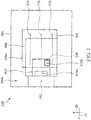
- FIG. 1 is a plan view of an exemplary semiconductor package structure 100 in accordance with some embodiments of the disclosure
- FIG. 2A is a cross-sectional view of an exemplary semiconductor package structure 100 shown in FIG. 1
- the semiconductor package structure 100 is a semiconductor package structure using a flip-chip technology, a wire-bonding technology, or a combination thereof.
- the semiconductor package structure 100 may be a system in package (SiP) package with an integrated radio frequency (RF) circuit.
- SiP system in package
- RF radio frequency
- the semiconductor package structure 100 includes a package substrate 200.
- the package substrate 200 may be mounted on a base (not shown).
- the base may include a printed circuit board (PCB) and may be formed of polypropylene (PP).
- the package substrate 200 may be mounted on a base (not shown) by a bonding process.
- the package substrate 200 may include conductive structures (not shown) that are mounted on and electrically coupled to the base by a bonding process.
- the conductive structures includes a conductive bump structure (such as a copper or solder bump structure), a conductive pillar structure, a conductive wire structure or a conductive paste structure.
- the semiconductor package structure 100 may include a system-on-chip (SOC) die including a RF circuit and a memory die in a stacking arrangement.
- the semiconductor package structure 100 includes a memory die 300 and an integrated circuit (IC) die 400 (such as a SOC die) having a RF circuit 410 which are successively and vertically stacked over the package substrate 200 by a bonding process using respective conductive structures (not shown).
- the conductive structure may include a conductive bump structure (such as a copper or solder bump structure), a conductive pillar structure, a conductive wire structure or a conductive paste structure.
- the memory die 300 may include a random access memory (RAM) die.
- the SOC die for example, may include a logic die including a central processing unit (CPU), a graphics processing unit (GPU), a RAM controller or any combination thereof. It should be noted that the number of dies integrated in the semiconductor package structure 100 is not limited to that disclosed in the embodiment.
- the memory die 300 entirely covers a first surface portion 200a of the package substrate 200 so as to define a second surface portion 200b of the package substrate 200 that is exposed from the memory die 300. Namely, as viewed from a top-view perspective, the memory die 300 has a projection on the package substrate 200 without overlapping the second surface portion 200b of the package substrate 200. Furthermore, the first surface portion 200a of the package substrate 200 may includes the routing on the substrate.
- the IC die 400 stacked on the memory die 300 partially covers the first surface portion 200a and the second surface 200b portion of the package substrate 200, so that the IC die 400 offsets the underlying memory die 300 along a predetermined direction.
- the IC die 400 offsets the underlying memory die 300 along a first direction 10, so that the IC die 400 has an edge that is aligned to an edge of the memory die 300, as shown in FIG. 1 .
- the IC die 400 offsets the underlying memory die 300 along a second direction 20 that is perpendicular to the first direction 10, so that the IC die 400 has an edge that is aligned to an edge of the memory die 300.
- the IC die 400 offsets the underlying memory die 300 along the first direction 10 and the second direction 20, so that the edges of the IC die 400 do not be aligned to edges of the memory die 300.
- the RF circuit 410 of the IC die 400 includes a first sensitive device region 410a and second sensitive device region 410b.
- the first sensitive device region 410a and the second sensitive device region 410b may each include one or more RF devices, such as RF transmitters (TXs), RF receivers (RXs), RF synthesizers (SXs), RF baluns, and RF inductors.
- TXs RF transmitters
- RXs RF receivers
- SXs RF synthesizers
- RF baluns RF baluns
- RF inductors such as RF transmitters (TXs), RF receivers (RXs), RF synthesizers (SXs), RF baluns, and RF inductors.
- the first sensitive device region 410a is located at a region of the RF circuit 410 corresponding to the second surface portion 200b of the package substrate 200.
- the second sensitive device region 410b is located at another region of the RF circuit 410 corresponding to the first surface portion 200a of the package substrate 200 and offsetting a memory input/output (I/O) electrical path of the memory die 300 (which is also referred to as a memory signal loop).
- the memory I/O electrical path at least includes one or more redistribution layers (RDLs) 310.
- RDLs redistribution layers
- FIG. 1 shows three RDLs 310 and the RDLs 310 are in a straight line arrangement and parallel to each other, it should be noted that the number and the arrangement of RDLs formed in the memory die is not limited to that disclosed in the embodiment and may be varied based on the design demands.
- the memory die 300 further includes an optional metal plate 320 disposed at a region of the memory die 300 directly below the second sensitive device region 410b.
- the area of the metal plate 320 may be larger than that of the second sensitive device region 410b.
- the metal plate 320 and the RDLs 310 may be formed by patterning the same conductive layer.
- the metal plate 320 is electrical isolated from the I/O electrical path of the memory die 300 and electrically connected to ground.
- the second sensitive device region 410b may be located at a region of the RF circuit 410 corresponding to the first surface portion 200a and the second surface portion 200b of the package substrate 200 and offsetting the memory I/O electrical path (e.g., the RDLs 310). Moreover, as viewed from a top-view perspective, the second sensitive device region 410b is spaced apart from the first sensitive device region 410a.
- the first sensitive device region 410a includes a circuit having one or more RF transmitters and one or more RF receivers and the second sensitive device region 410b includes one or more RF synthesizers.
- the first sensitive device region 410a may also include one or more RF baluns and the second sensitive device region may also include includes one or more RF inductors.
- the first sensitive device region 410a includes a circuit having one or more RF synthesizers and one or more RF receivers and the second sensitive device region 410b includes one or more RF transmitters.
- the first sensitive device region 410a may also include one or more RF inductors and the second sensitive device region may also include includes one or more RF baluns.
- the first sensitive device region 410a includes a circuit having one or more RF receivers and the second sensitive device region 410b includes one or more RF transmitters and one or more RF synthesizers.
- the second sensitive device region may also include one or more RF inductors and one or more RF baluns.
- the first sensitive device region 410a includes a circuit having one or more RF receivers, one or more RF transmitters, and one or more RF synthesizers.
- the second surface portion 200b of the package substrate 200 has an interconnect region 202 located adjacent to an edge of the package substrate 200.
- the interconnect region 202 provides an electrically connection between the conductive structures (not shown) of the package substrate 200 and the first and second sensitive device regions 410a and 410b of the RF circuit 410, in which these conductive structures are mounted on and electrically coupled to the base (not shown).
- the interconnect region 202 and the first and second sensitive device regions 410a and 410b of the RF circuit 410 construct a RF sensitive signal loop, which does not overlap with the memory signal loop (i.e., the I/O electrical path of the memory die 300) as viewed from a top-view perspective.
- the first sensitive device region 410a of the RF circuit 410 is located between the interconnect region 202 and the memory die 300, as shown in FIG. 1 .
- the first sensitive device region 410a is covered by the first sensitive device region 410a.
- the semiconductor package structure 100 may include an encapsulating layer (not shown), such as a molding compound, disposed on the package substrate 200 and surrounding the memory die 300 and the overlying IC die 400.
- the molding compound may be formed of an epoxy, a resin, a moldable polymer, or the like.
- the package substrate 200 may be equipped with a RF die (not shown).
- the IC die 400 does not have the RF circuit 410 including the first sensitive device region 410a and second sensitive device region 410b.
- the RF die may include the RF circuit 410.
- the RF die is disposed on the second surface portion 200b of the package substrate 200 that is exposed from the memory die 300. Namely, as viewed from a top-view perspective, the memory die 300 has a projection on the package substrate 200 without overlapping with the RF die.
- the first sensitive device region 41 0a and the second sensitive device region 410b are located at the region of the RF circuit 410 corresponding to the second surface portion 200b of the package substrate 200.
- the RF die is located between the interconnect region 202 and the memory die 300.
- at least a portion of the interconnect region 202 is covered by the first sensitive device region 410a of the RF die.
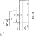
- FIG. 2B illustrates a cross-sectional view of an exemplary semiconductor package structure 100' in accordance with some embodiments of the disclosure. Descriptions of elements of the embodiments hereinafter that are the same as or similar to those previously described with reference to FIGS. 1 and 2A may be omitted for brevity.
- the semiconductor package structure 100' is similar to the semiconductor package structure 100 shown in FIGS. 1 and 2A . Compared to the semiconductor package structure 100, the semiconductor package structure 100' further includes a spacer 350 interposed between the IC die 400 and the memory die 300, as shown in FIG. 2B .
- the spacer 350 is a dummy die and there is not any passive component, active component, or circuit.
- the edges of the memory die 300 are not aligned to the edges of the spacer 350 and the edges of the IC die 400 are also not aligned to the edges of the spacer 350, as shown in FIG. 2B .
- the edges of the memory die 300 laterally protrude from the edges of the spacer 350.
- the memory die 300 may provide space for bonding wires (not shown).
- an edge of the spacer 350 may be aligned to an edge of the memory die 300 or an edge of the IC die 400. It should be noted that the planar arrangement of the spacer 350 is not limited to that disclosed in the embodiment.
- the spacer 350 may be a die having an RDL structure (not shown) that is coupled between the IC die 400 and the memory die 300.
- the RDL structure may be referred to as a fan-out structure.
- the RDL structure includes one or more conductive traces disposed in an inter-metal dielectric (IMD) layer.
- IMD inter-metal dielectric
- the conductive traces may be disposed at multiple levels of the IMD layer.
- the IMD layer may be a single layer or a multi-layer structure.
- the IMD layer may be formed of organic materials, which include a polymer base material, non-organic materials, which include silicon nitride (SiN x ), silicon oxide (SiOx), graphene, or the like.
- the IMD layer is a high-k dielectric layer (k is the dielectric constant of the dielectric layer).
- the IMD layer may be formed of a photo sensitive material, which includes a dry film photoresist, or a taping film.
- the semiconductor package structure 100' may include an encapsulating layer (not shown), such as a molding compound, disposed on the package substrate 200 and surrounding the memory die 300, the spacer 350, and the overlying IC die 400.
- an encapsulating layer such as a molding compound
- FIG. 2C illustrates a cross-sectional view of an exemplary semiconductor package structure 100" in accordance with some embodiments of the disclosure. Descriptions of elements of the embodiments hereinafter that are the same as or similar to those previously described with reference to FIGS. 1 and 2A or FIG. 2B may be omitted for brevity.
- the semiconductor package structure 100" is similar to the semiconductor package structure 100' shown in FIG. 2B .
- the memory die 300 in the semiconductor package structure 100" does not have the metal plate 320.
- the spacer 350 in the semiconductor package structure 100" is a dummy die and includes the optional metal plate 320 at a region of the spacer 350 directly below the second sensitive device region 410b.
- the area of the metal plate 320 may be larger than that of the second sensitive device region 410b.
- the metal plate 320 is electrically connected to ground.
- FIG. 3 is a plan view of an exemplary semiconductor package structure 100a in accordance with some embodiments of the disclosure
- FIG. 4A is a cross-sectional view of an exemplary semiconductor package structure 100a shown in FIG. 3 .
- the semiconductor package structure 100a is similar to the semiconductor package structure 100 shown in FIGS. 1 and 2A .
- the semiconductor package structure 100a is a semiconductor package structure using a flip-chip technology, a wire-bonding technology, or a combination thereof.
- the semiconductor package structure 100a may be a system in package (SiP) package with an integrated a radio frequency (RF) circuit.
- the package substrate 200 of the semiconductor package structure 100a may be mounted on a base (not shown) that may include a PCB.
- an IC die 400 (such as a SOC die) and a memory die 300 in the semiconductor package structure 100a are successively and vertically stacked over the package substrate 200, as shown in FIG. 4A .
- the memory die 300 may not have the metal plate 320.
- the memory die 300 may include a random access memory (RAM) die.
- the SOC die for example, may include a logic die including a central processing unit (CPU), a graphics processing unit (GPU), a RAM controller or any combination thereof. It should be noted that the number of dies integrated in the semiconductor package structure 100 is not limited to that disclosed in the embodiment.
- the memory die 300 overlying the IC die 400 entirely covers a first surface portion 200a of the package substrate 200 so as to define a second surface portion 200b of the package substrate 200 that is exposed from the memory die 300.
- the IC die 400 underlying the memory die 300 partially covers the first surface portion 200a and the second surface 200b portion of the package substrate 200, so that the IC die 400 offsets the overlying memory die 300 along a predetermined direction.
- the IC die 400 offsets the overlying memory die 300 along a first direction 10, so that the IC die 400 has an edge that is aligned to an edge of the memory die 300, as shown in FIG. 3 .
- the IC die 400 offsets the overlying memory die 300 along a second direction 20 that is perpendicular to the first direction 10, so that the IC die 400 has an edge that is aligned to an edge of the memory die 300.
- the IC die 400 offsets the overlying memory die 300 along the first direction 10 and the second direction 20, so that the edges of the IC die 400 do not be aligned to edges of the memory die 300.
- the package substrate 200 may be equipped with a RF die (not shown).
- the IC die 400 may be entirely within the first surface portion 200a of the package substrate 200, so as to be entirely covered by the overlying memory die 300.
- the IC die 400 does not have the RF circuit 410 including the first sensitive device region 410a and second sensitive device region 410b.
- the RF die may include the RF circuit 410.
- the RF die is disposed on the second surface portion 200b of the package substrate 200 that is exposed from the memory die 300. Namely, as viewed from a top-view perspective, the memory die 300 has a projection on the package substrate 200 without overlapping with the RF die.
- the first sensitive device region 410a and the second sensitive device region 410b are located at the region of the RF circuit 410 corresponding to the second surface portion 200b of the package substrate 200.
- the RF die is located between the interconnect region 202 and the memory die 300.
- at least a portion of the interconnect region 202 is covered by the first sensitive device region 410a of the RF die.
- FIG. 4B illustrates a cross-sectional view of an exemplary semiconductor package structure 100a' in accordance with some embodiments of the disclosure. Descriptions of elements of the embodiments hereinafter that are the same as or similar to those previously described with reference to FIGS. 2B , 3 , and 4A may be omitted for brevity.
- the semiconductor package structure 100a' is similar to the semiconductor package structure 100 shown in FIGS. 3 and 4A . Compared to the semiconductor package structure 100a, the semiconductor package structure 100a' further includes a spacer 350 interposed between the IC die 400 and the memory die 300, as shown in FIG. 4B .
- the spacer 350 is a dummy die or a die having an RDL structure (not shown) that is coupled between the IC die 400 and the memory die 300.
- the edges of the IC die 400 are not aligned to the edges of the spacer 350, as shown in FIG. 4B .
- the edges of the IC die 400 laterally protrude from the edges of the spacer 350.
- the IC die 400 may provide spaces for bonding wires (not shown).
- an edge of the spacer 350 may be aligned to an edge of the memory die 300. It should be noted that the planar arrangement of the spacer 350 is not limited to that disclosed in the embodiment.
- the semiconductor package structure 100a' may include an encapsulating layer (not shown), such as a molding compound, disposed on the package substrate 200 and surrounding the memory die 300, the spacer 350, and the overlying IC die 400.
- an encapsulating layer such as a molding compound
- the first and second sensitive device regions of the RF circuit that is integrated into an SOC die are arranged to be spaced apart from the memory I/O electrical path of a memory die stacked above or below the SOC die.
- the metal plate can serve as a shielding layer so as to further eliminate or mitigate undesired signal coupling between the memory I/O electrical path and the sensitive device and/or routing in RF circuit.
- a portion of RF circuit including the second sensitive device region is arranged to overlap the memory die stacked above or below the RF circuit. Accordingly, compared to cases where the RF circuit does not overlap the memory die, as viewed from a top-view perspective, a compact package size can be obtained.
- the design flexibility of the wire's loop height for bonding wires in the semiconductor package structure can be increased.
Landscapes
- Semiconductor Integrated Circuits (AREA)
- Semiconductor Memories (AREA)
- Structures Or Materials For Encapsulating Or Coating Semiconductor Devices Or Solid State Devices (AREA)
- Physics & Mathematics (AREA)
- Health & Medical Sciences (AREA)
- Electromagnetism (AREA)
- Toxicology (AREA)
Abstract
Description
- This application claims the benefit of
U.S. Provisional Application No. 62/382,285 filed on September 1, 2016 - The present invention relates to semiconductor packaging technology, and in particular to a memory die integrated into a semiconductor package structure having a radio frequency (RF) function.
- In recent years, as electronic products have become increasingly multifunctional and have been scaled down in size, there is a desire for manufacturers of semiconductor devices to make more devices formed in a single semiconductor package, so that the electronic products that employ these devices can provide several advantages in terms of cost, size, performance, and product-design flexibility.
- Response to this desire has been the development of stacked-die packaging technology. Stacked-die packaging technology enables two or more dies with different functions to be installed atop one another, i.e. stacked. This allows higher component density in electronic products, such as mobile phones, personal digital assistants (PDAs), and digital cameras.
- Such electronic products are also provided with wireless communications capabilities. For achieving the function of wireless communications, a communication module (e.g., an IC package with radio frequency (RF) devices) is typically required.
- However, some problems may occur while manufacturing the semiconductor package utilizing the stacked-die packaging technology. For example, as a semiconductor memory die is integrated into a semiconductor package with a RF function by the stacked-die packaging technology, RF desense (i.e., degradation of sensitivity) may easily occur due to undesired signal coupling between the semiconductor memory die and the sensitive RF device (such as RF transmitter (TX), RF receiver (RX), RF synthesizer (SX), RF balun or RF inductor) or RF routing in different parts of the semiconductor package or in another die (e.g., SoC (system-on-chip) die). This problem can result in a degradation of RF performance. Thus, a novel semiconductor package structure is desirable.
- Semiconductor package structures are provided. An exemplary embodiment of a semiconductor package structure includes a package substrate. An integrated circuit (IC) die has a radio frequency (RF) circuit and a memory die stacked over the package substrate. The memory die entirely covers a first surface portion of the package substrate to define a second surface portion of the package substrate exposed from the memory die and the IC die partially covers the first surface portion and the second surface portion of the package substrate. The RF circuit includes a first sensitive device region corresponding to the second surface portion of the package substrate and a second sensitive device region corresponding to the first surface portion of the package substrate and offsetting a memory input/output (I/O) electrical path of the memory die, as viewed from a top-view perspective.
- Another exemplary embodiment of a semiconductor package structure includes a package substrate. An IC die having a RF circuit and a memory die stacked over the package substrate. The memory die is disposed over the IC die and the memory die has a memory I/O electrical path. The RF circuit includes a first sensitive device region corresponding to a second surface portion of the package substrate and a second sensitive device region corresponding to a first surface portion of the package substrate and offsetting the memory I/O electrical path of the memory die, as viewed from a top-view perspective.
- Yet another exemplary embodiment of a semiconductor package structure includes a package substrate. An IC die has a RF circuit and a memory die stacked over the package substrate. The IC die is disposed over the memory die and the memory die has a memory I/O electrical path. The RF circuit includes a first sensitive device region corresponding to a second surface portion of the package substrate and a second sensitive device region corresponding to a first surface portion of the package substrate and offsetting the memory I/O electrical path of the memory die, as viewed from a top-view perspective.
- A detailed description is given in the following embodiments with reference to the accompanying drawings.
- The present invention can be more fully understood by reading the subsequent detailed description and examples with references made to the accompanying drawings, wherein:
-
FIG. 1 is a plan view of an exemplary semiconductor package structure in accordance with some embodiments of the disclosure. -
FIG. 2A is a cross-sectional view of an exemplary semiconductor package structure shown inFIG. 1 . -
FIG. 2B is a cross-sectional view of an exemplary semiconductor package structure in accordance with some embodiments of the disclosure. -
FIG. 2C is a cross-sectional view of an exemplary semiconductor package structure in accordance with some embodiments of the disclosure. -
FIG. 3 is a plan view of an exemplary semiconductor package structure in accordance with some embodiments of the disclosure. -
FIG. 4A is a cross-sectional view of an exemplary semiconductor package structure shown inFIG. 3 . -
FIG. 4B is a cross-sectional view of an exemplary semiconductor package structure in accordance with some embodiments of the disclosure. - The following description is of the best-contemplated mode of carrying out the invention. This description is made for the purpose of illustrating the general principles of the invention and should not be taken in a limiting sense. The scope of the invention is determined by reference to the appended claims.
- The present invention will be described with respect to particular embodiments and with reference to certain drawings, but the invention is not limited thereto and is only limited by the claims. The drawings described are only schematic and are non-limiting. In the drawings, the size of some of the elements may be exaggerated for illustrative purposes and not drawn to scale. The dimensions and the relative dimensions do not correspond to actual dimensions in the practice of the invention.
- Refer to
FIGS. 1 and2A , in whichFIG. 1 is a plan view of an exemplarysemiconductor package structure 100 in accordance with some embodiments of the disclosure, andFIG. 2A is a cross-sectional view of an exemplarysemiconductor package structure 100 shown inFIG. 1 . In some embodiments, thesemiconductor package structure 100 is a semiconductor package structure using a flip-chip technology, a wire-bonding technology, or a combination thereof. Moreover, thesemiconductor package structure 100 may be a system in package (SiP) package with an integrated radio frequency (RF) circuit. - As shown in
FIGS. 1 and2A , in some embodiments, thesemiconductor package structure 100 includes apackage substrate 200. Thepackage substrate 200 may be mounted on a base (not shown). For example, the base may include a printed circuit board (PCB) and may be formed of polypropylene (PP). Moreover, thepackage substrate 200 may be mounted on a base (not shown) by a bonding process. Thepackage substrate 200 may include conductive structures (not shown) that are mounted on and electrically coupled to the base by a bonding process. In some embodiments, the conductive structures, includes a conductive bump structure (such as a copper or solder bump structure), a conductive pillar structure, a conductive wire structure or a conductive paste structure. - In some embodiments, the
semiconductor package structure 100 may include a system-on-chip (SOC) die including a RF circuit and a memory die in a stacking arrangement. For example, thesemiconductor package structure 100 includes a memory die 300 and an integrated circuit (IC) die 400 (such as a SOC die) having aRF circuit 410 which are successively and vertically stacked over thepackage substrate 200 by a bonding process using respective conductive structures (not shown). The conductive structure may include a conductive bump structure (such as a copper or solder bump structure), a conductive pillar structure, a conductive wire structure or a conductive paste structure. - The memory die 300, for example, may include a random access memory (RAM) die. Moreover, the SOC die, for example, may include a logic die including a central processing unit (CPU), a graphics processing unit (GPU), a RAM controller or any combination thereof. It should be noted that the number of dies integrated in the
semiconductor package structure 100 is not limited to that disclosed in the embodiment. - As shown in
FIG. 1 , the memory die 300 entirely covers afirst surface portion 200a of thepackage substrate 200 so as to define asecond surface portion 200b of thepackage substrate 200 that is exposed from the memory die 300. Namely, as viewed from a top-view perspective, the memory die 300 has a projection on thepackage substrate 200 without overlapping thesecond surface portion 200b of thepackage substrate 200. Furthermore, thefirst surface portion 200a of thepackage substrate 200 may includes the routing on the substrate. - Moreover, the IC die 400 stacked on the memory die 300 partially covers the
first surface portion 200a and thesecond surface 200b portion of thepackage substrate 200, so that the IC die 400 offsets the underlying memory die 300 along a predetermined direction. In some embodiments, the IC die 400 offsets the underlying memory die 300 along afirst direction 10, so that the IC die 400 has an edge that is aligned to an edge of the memory die 300, as shown inFIG. 1 . In some embodiments, the IC die 400 offsets the underlying memory die 300 along asecond direction 20 that is perpendicular to thefirst direction 10, so that the IC die 400 has an edge that is aligned to an edge of the memory die 300. Alternatively, the IC die 400 offsets the underlying memory die 300 along thefirst direction 10 and thesecond direction 20, so that the edges of the IC die 400 do not be aligned to edges of the memory die 300. - As shown in
FIGS. 1 and2A , theRF circuit 410 of the IC die 400 includes a firstsensitive device region 410a and secondsensitive device region 410b. In some embodiments, the firstsensitive device region 410a and the secondsensitive device region 410b may each include one or more RF devices, such as RF transmitters (TXs), RF receivers (RXs), RF synthesizers (SXs), RF baluns, and RF inductors. In some embodiments, as viewed from a top-view perspective, the firstsensitive device region 410a is located at a region of theRF circuit 410 corresponding to thesecond surface portion 200b of thepackage substrate 200. Moreover, as viewed from a top-view perspective, the secondsensitive device region 410b is located at another region of theRF circuit 410 corresponding to thefirst surface portion 200a of thepackage substrate 200 and offsetting a memory input/output (I/O) electrical path of the memory die 300 (which is also referred to as a memory signal loop). In some embodiments, the memory I/O electrical path at least includes one or more redistribution layers (RDLs) 310. AlthoughFIG. 1 shows threeRDLs 310 and theRDLs 310 are in a straight line arrangement and parallel to each other, it should be noted that the number and the arrangement of RDLs formed in the memory die is not limited to that disclosed in the embodiment and may be varied based on the design demands. - In some embodiments, the memory die 300 further includes an
optional metal plate 320 disposed at a region of the memory die 300 directly below the secondsensitive device region 410b. The area of themetal plate 320 may be larger than that of the secondsensitive device region 410b. Moreover, themetal plate 320 and theRDLs 310 may be formed by patterning the same conductive layer. In some embodiments, themetal plate 320 is electrical isolated from the I/O electrical path of the memory die 300 and electrically connected to ground. - Alternatively, as viewed from a top-view perspective, the second
sensitive device region 410b may be located at a region of theRF circuit 410 corresponding to thefirst surface portion 200a and thesecond surface portion 200b of thepackage substrate 200 and offsetting the memory I/O electrical path (e.g., the RDLs 310). Moreover, as viewed from a top-view perspective, the secondsensitive device region 410b is spaced apart from the firstsensitive device region 410a. - In some embodiments, the first
sensitive device region 410a includes a circuit having one or more RF transmitters and one or more RF receivers and the secondsensitive device region 410b includes one or more RF synthesizers. In these cases, the firstsensitive device region 410a may also include one or more RF baluns and the second sensitive device region may also include includes one or more RF inductors. - In some embodiments, the first
sensitive device region 410a includes a circuit having one or more RF synthesizers and one or more RF receivers and the secondsensitive device region 410b includes one or more RF transmitters. In these cases, the firstsensitive device region 410a may also include one or more RF inductors and the second sensitive device region may also include includes one or more RF baluns. - In some embodiments, the first
sensitive device region 410a includes a circuit having one or more RF receivers and the secondsensitive device region 410b includes one or more RF transmitters and one or more RF synthesizers. In these cases, the second sensitive device region may also include one or more RF inductors and one or more RF baluns. - Alternatively, the first
sensitive device region 410a includes a circuit having one or more RF receivers, one or more RF transmitters, and one or more RF synthesizers. - As shown in
FIGS. 1 and2A , in some embodiments, as viewed from a top-view perspective, thesecond surface portion 200b of thepackage substrate 200 has aninterconnect region 202 located adjacent to an edge of thepackage substrate 200. Theinterconnect region 202 provides an electrically connection between the conductive structures (not shown) of thepackage substrate 200 and the first and secondsensitive device regions RF circuit 410, in which these conductive structures are mounted on and electrically coupled to the base (not shown). Accordingly, theinterconnect region 202 and the first and secondsensitive device regions RF circuit 410 construct a RF sensitive signal loop, which does not overlap with the memory signal loop (i.e., the I/O electrical path of the memory die 300) as viewed from a top-view perspective. - In some embodiments, as viewed from a top-view perspective, the first
sensitive device region 410a of theRF circuit 410 is located between theinterconnect region 202 and the memory die 300, as shown inFIG. 1 . Alternatively, as viewed from a top-view perspective, at least a portion of theinterconnect region 202 is covered by the firstsensitive device region 410a. - In some embodiments, the
semiconductor package structure 100 may include an encapsulating layer (not shown), such as a molding compound, disposed on thepackage substrate 200 and surrounding the memory die 300 and the overlying IC die 400. In some embodiments, the molding compound may be formed of an epoxy, a resin, a moldable polymer, or the like. - In some other embodiments, the
package substrate 200 may be equipped with a RF die (not shown). In those cases, the IC die 400 does not have theRF circuit 410 including the firstsensitive device region 410a and secondsensitive device region 410b. Moreover, the RF die may include theRF circuit 410. The RF die is disposed on thesecond surface portion 200b of thepackage substrate 200 that is exposed from the memory die 300. Namely, as viewed from a top-view perspective, the memory die 300 has a projection on thepackage substrate 200 without overlapping with the RF die. In more detail, in some embodiments, the first sensitive device region 41 0a and the secondsensitive device region 410b are located at the region of theRF circuit 410 corresponding to thesecond surface portion 200b of thepackage substrate 200. In some embodiments, as viewed from a top-view perspective, the RF die is located between theinterconnect region 202 and the memory die 300. Alternatively, as viewed from a top-view perspective, at least a portion of theinterconnect region 202 is covered by the firstsensitive device region 410a of the RF die. -
FIG. 2B illustrates a cross-sectional view of an exemplary semiconductor package structure 100' in accordance with some embodiments of the disclosure. Descriptions of elements of the embodiments hereinafter that are the same as or similar to those previously described with reference toFIGS. 1 and2A may be omitted for brevity. In the embodiment, the semiconductor package structure 100' is similar to thesemiconductor package structure 100 shown inFIGS. 1 and2A . Compared to thesemiconductor package structure 100, the semiconductor package structure 100' further includes aspacer 350 interposed between the IC die 400 and the memory die 300, as shown inFIG. 2B . - In some embodiments, the
spacer 350 is a dummy die and there is not any passive component, active component, or circuit. Moreover, the edges of the memory die 300 are not aligned to the edges of thespacer 350 and the edges of the IC die 400 are also not aligned to the edges of thespacer 350, as shown inFIG. 2B . For example, the edges of the memory die 300 laterally protrude from the edges of thespacer 350. As a result, the memory die 300 may provide space for bonding wires (not shown). - Alternatively, an edge of the
spacer 350 may be aligned to an edge of the memory die 300 or an edge of the IC die 400. It should be noted that the planar arrangement of thespacer 350 is not limited to that disclosed in the embodiment. - In some embodiments, the
spacer 350 may be a die having an RDL structure (not shown) that is coupled between the IC die 400 and the memory die 300. The RDL structure may be referred to as a fan-out structure. In some embodiments, the RDL structure includes one or more conductive traces disposed in an inter-metal dielectric (IMD) layer. For example, the conductive traces may be disposed at multiple levels of the IMD layer. In some embodiments, the IMD layer may be a single layer or a multi-layer structure. Moreover, the IMD layer may be formed of organic materials, which include a polymer base material, non-organic materials, which include silicon nitride (SiNx), silicon oxide (SiOx), graphene, or the like. - In some other embodiments, the IMD layer is a high-k dielectric layer (k is the dielectric constant of the dielectric layer). Alternatively, the IMD layer may be formed of a photo sensitive material, which includes a dry film photoresist, or a taping film.
- In some embodiments, the semiconductor package structure 100' may include an encapsulating layer (not shown), such as a molding compound, disposed on the
package substrate 200 and surrounding the memory die 300, thespacer 350, and the overlying IC die 400. -
FIG. 2C illustrates a cross-sectional view of an exemplarysemiconductor package structure 100" in accordance with some embodiments of the disclosure. Descriptions of elements of the embodiments hereinafter that are the same as or similar to those previously described with reference toFIGS. 1 and2A orFIG. 2B may be omitted for brevity. In the embodiment, thesemiconductor package structure 100" is similar to the semiconductor package structure 100' shown inFIG. 2B . Compared to the semiconductor package structure 100', the memory die 300 in thesemiconductor package structure 100" does not have themetal plate 320. Moreover, thespacer 350 in thesemiconductor package structure 100" is a dummy die and includes theoptional metal plate 320 at a region of thespacer 350 directly below the secondsensitive device region 410b. The area of themetal plate 320 may be larger than that of the secondsensitive device region 410b. In some embodiments, themetal plate 320 is electrically connected to ground. - Refer to
FIGS. 3 and4A , in whichFIG. 3 is a plan view of an exemplarysemiconductor package structure 100a in accordance with some embodiments of the disclosure, andFIG. 4A is a cross-sectional view of an exemplarysemiconductor package structure 100a shown inFIG. 3 . Descriptions of elements of the embodiments hereinafter that are the same as or similar to those previously described with reference toFIGS. 1 and2A may be omitted for brevity. In the embodiment, thesemiconductor package structure 100a is similar to thesemiconductor package structure 100 shown inFIGS. 1 and2A . In some embodiments, thesemiconductor package structure 100a is a semiconductor package structure using a flip-chip technology, a wire-bonding technology, or a combination thereof. Moreover, thesemiconductor package structure 100a may be a system in package (SiP) package with an integrated a radio frequency (RF) circuit. Similarly, thepackage substrate 200 of thesemiconductor package structure 100a may be mounted on a base (not shown) that may include a PCB. - Unlike the
semiconductor package structure 100, an IC die 400 (such as a SOC die) and amemory die 300 in thesemiconductor package structure 100a are successively and vertically stacked over thepackage substrate 200, as shown inFIG. 4A . Moreover, the memory die 300 may not have themetal plate 320. - The memory die 300, for example, may include a random access memory (RAM) die. Moreover, the SOC die, for example, may include a logic die including a central processing unit (CPU), a graphics processing unit (GPU), a RAM controller or any combination thereof. It should be noted that the number of dies integrated in the
semiconductor package structure 100 is not limited to that disclosed in the embodiment. - As shown in
FIG. 3 , as viewed from a top-view perspective, the memory die 300 overlying the IC die 400 entirely covers afirst surface portion 200a of thepackage substrate 200 so as to define asecond surface portion 200b of thepackage substrate 200 that is exposed from the memory die 300. Moreover, the IC die 400 underlying the memory die 300 partially covers thefirst surface portion 200a and thesecond surface 200b portion of thepackage substrate 200, so that the IC die 400 offsets the overlying memory die 300 along a predetermined direction. For example, the IC die 400 offsets the overlying memory die 300 along afirst direction 10, so that the IC die 400 has an edge that is aligned to an edge of the memory die 300, as shown inFIG. 3 . In some embodiments, the IC die 400 offsets the overlying memory die 300 along asecond direction 20 that is perpendicular to thefirst direction 10, so that the IC die 400 has an edge that is aligned to an edge of the memory die 300. Alternatively, the IC die 400 offsets the overlying memory die 300 along thefirst direction 10 and thesecond direction 20, so that the edges of the IC die 400 do not be aligned to edges of the memory die 300. - In some other embodiments, the
package substrate 200 may be equipped with a RF die (not shown). In those cases, the IC die 400 may be entirely within thefirst surface portion 200a of thepackage substrate 200, so as to be entirely covered by the overlying memory die 300. Moreover, the IC die 400 does not have theRF circuit 410 including the firstsensitive device region 410a and secondsensitive device region 410b. The RF die may include theRF circuit 410. The RF die is disposed on thesecond surface portion 200b of thepackage substrate 200 that is exposed from the memory die 300. Namely, as viewed from a top-view perspective, the memory die 300 has a projection on thepackage substrate 200 without overlapping with the RF die. In more detail, in some embodiments, the firstsensitive device region 410a and the secondsensitive device region 410b are located at the region of theRF circuit 410 corresponding to thesecond surface portion 200b of thepackage substrate 200. In some embodiments, as viewed from a top-view perspective, the RF die is located between theinterconnect region 202 and the memory die 300. In some other embodiments, as viewed from a top-view perspective, at least a portion of theinterconnect region 202 is covered by the firstsensitive device region 410a of the RF die. -
FIG. 4B illustrates a cross-sectional view of an exemplarysemiconductor package structure 100a' in accordance with some embodiments of the disclosure. Descriptions of elements of the embodiments hereinafter that are the same as or similar to those previously described with reference toFIGS. 2B ,3 , and4A may be omitted for brevity. In the embodiment, thesemiconductor package structure 100a' is similar to thesemiconductor package structure 100 shown inFIGS. 3 and4A . Compared to thesemiconductor package structure 100a, thesemiconductor package structure 100a' further includes aspacer 350 interposed between the IC die 400 and the memory die 300, as shown inFIG. 4B . - In some embodiments, the
spacer 350 is a dummy die or a die having an RDL structure (not shown) that is coupled between the IC die 400 and the memory die 300. Moreover, the edges of the IC die 400 are not aligned to the edges of thespacer 350, as shown inFIG. 4B . For example, the edges of the IC die 400 laterally protrude from the edges of thespacer 350. As a result, the IC die 400 may provide spaces for bonding wires (not shown). Moreover, an edge of thespacer 350 may be aligned to an edge of the memory die 300. It should be noted that the planar arrangement of thespacer 350 is not limited to that disclosed in the embodiment. - In some embodiments, the
semiconductor package structure 100a' may include an encapsulating layer (not shown), such as a molding compound, disposed on thepackage substrate 200 and surrounding the memory die 300, thespacer 350, and the overlying IC die 400. - According to the foregoing embodiments, as viewed from a top-view perspective, the first and second sensitive device regions of the RF circuit that is integrated into an SOC die are arranged to be spaced apart from the memory I/O electrical path of a memory die stacked above or below the SOC die. As a result, undesired signal coupling between the memory I/O electrical path and the sensitive device and/or routing in RF circuit can be eliminated or mitigated, thereby preventing RF desense and improving or maintaining RF performance. Moreover, since a metal plate connected to ground is disposed directly below the second sensitive device regions of the RF circuit, the metal plate can serve as a shielding layer so as to further eliminate or mitigate undesired signal coupling between the memory I/O electrical path and the sensitive device and/or routing in RF circuit.
- Moreover, according to the foregoing embodiments, as viewed from a top-view perspective, a portion of RF circuit including the second sensitive device region is arranged to overlap the memory die stacked above or below the RF circuit. Accordingly, compared to cases where the RF circuit does not overlap the memory die, as viewed from a top-view perspective, a compact package size can be obtained.
- Additionally, according to the foregoing embodiments, since a dummy die is interposed between the memory die and the IC die, the design flexibility of the wire's loop height for bonding wires in the semiconductor package structure can be increased.
- While the invention has been described by way of example and in terms of the preferred embodiments, it is to be understood that the invention is not limited to the disclosed embodiments. On the contrary, it is intended to cover various modifications and similar arrangements (as would be apparent to those skilled in the art). Therefore, the scope of the appended claims should be accorded the broadest interpretation so as to encompass all such modifications and similar arrangements.
Claims (15)
- A semiconductor package structure, comprising:a package substrate; andan integrated circuit (IC) die having a radio frequency (RF) circuit and a memory die stacked over the package substrate,wherein the memory die entirely covers a first surface portion of the package substrate to define a second surface portion of the package substrate exposed from the memory die and the IC die partially covers the first surface portion and the second surface portion of the package substrate; andwherein the RF circuit comprises a first sensitive device region corresponding to the second surface portion of the package substrate and a second sensitive device region corresponding to the first surface portion of the package substrate and offsetting a memory input/output (I/O) electrical path of the memory die, as viewed from a top-view perspective.
- The semiconductor package structure as claimed in claim 1, wherein the IC die is disposed over the memory die.
- The semiconductor package structure as claimed in claim 2, further comprising a spacer interposed between the IC die and the memory die; wherein
the spacer is preferably a dummy die. - The semiconductor package structure as claimed in claim 3, wherein the spacer comprises a metal plate directly below the second sensitive device region of the RF circuit,
wherein the metal plate is preferably electrically connected to ground. - The semiconductor package structure as claimed in claim 3 or 4, wherein the spacer comprises a redistribution layer (RDL) structure that is coupled between the IC die and the memory die.
- The semiconductor package structure as claimed in any of the preceding claims, wherein the memory die comprises a metal plate directly below the second sensitive device region of the RF circuit,
wherein the metal plate is preferably electrically connected to ground. - The semiconductor package structure as claimed in any of the preceding claims, wherein the memory die comprises a metal plate directly below the second sensitive device region of the RF circuit, wherein the metal plate is preferably electrically connected to ground.
- The semiconductor package structure as claimed in any of the preceding claims, wherein the memory die is disposed over the IC die.
- The semiconductor package structure as claimed in claim 8, further comprising a spacer interposed between the IC die and the memory die,
wherein the spacer is preferably a dummy die. - The semiconductor package structure as claimed in claim 9, wherein the spacer comprises an RDL structure that is coupled between the IC die and the memory die.
- The semiconductor package structure as claimed in any of the preceding claims, wherein the first sensitive device region comprises an RF transmitter and an RF receiver and the second sensitive device region comprises an RF synthesizer,
wherein the first sensitive device region preferably further comprises an RF balun and the second sensitive device region preferably further comprises an RF inductor. - The semiconductor package structure as claimed in any of the preceding claims, wherein the first sensitive device region comprises an RF synthesizer and an RF receiver and the second sensitive device region comprises an RF transmitter,
wherein the first sensitive device region preferably further comprises an RF inductor and the second sensitive device region preferably further comprises an RF balun. - The semiconductor package structure as claimed in any of the preceding claims, wherein the first sensitive device region comprises an RF receiver and the second sensitive device region comprises an RF transmitter and an RF synthesizer;
wherein the second sensitive device region preferably further comprises an RF balun and an RF inductor. - The semiconductor package structure as claimed in any of the preceding claims, wherein the first sensitive device region comprises an RF receiver, an RF transmitter, and an RF synthesizer; and/or
wherein the memory I/O electrical path comprises an RDL. - The semiconductor package structure as claimed in any of the preceding claims, wherein the second sensitive device region further corresponds to the second surface portion of the package substrate and is spaced apart from the first sensitive device region, as viewed from a top-view perspective; and/or
wherein the second surface portion of the package substrate has an interconnect region coupled to the first sensitive device region and the second sensitive device region, and wherein the first sensitive device region is between the interconnect region and the memory die, as viewed from a top-view perspective; and/or
wherein the second surface portion of the package substrate has an interconnect region coupled to the first sensitive device region and the second sensitive device region, and wherein at least a portion of the interconnect region is covered by the first sensitive device region, as viewed from a top-view perspective.
Applications Claiming Priority (2)
| Application Number | Priority Date | Filing Date | Title |
|---|---|---|---|
| US201662382285P | 2016-09-01 | 2016-09-01 | |
| US15/682,908 US10446508B2 (en) | 2016-09-01 | 2017-08-22 | Semiconductor package integrated with memory die |
Publications (2)
| Publication Number | Publication Date |
|---|---|
| EP3291296A1 true EP3291296A1 (en) | 2018-03-07 |
| EP3291296B1 EP3291296B1 (en) | 2022-05-11 |
Family
ID=59846334
Family Applications (1)
| Application Number | Title | Priority Date | Filing Date |
|---|---|---|---|
| EP17188501.5A Active EP3291296B1 (en) | 2016-09-01 | 2017-08-30 | Semiconductor package with a memory die and an integrated circuit die having an rf circuit |
Country Status (4)
| Country | Link |
|---|---|
| US (1) | US10446508B2 (en) |
| EP (1) | EP3291296B1 (en) |
| CN (1) | CN108346650B (en) |
| TW (1) | TWI652794B (en) |
Families Citing this family (4)
| Publication number | Priority date | Publication date | Assignee | Title |
|---|---|---|---|---|
| CN114496816A (en) * | 2020-10-27 | 2022-05-13 | 合肥君正科技有限公司 | SiP packaging design method of camera chip |
| CN116108900A (en) * | 2021-11-05 | 2023-05-12 | 安徽寒武纪信息科技有限公司 | Accelerator structure, method and device for generating accelerator structure |
| US20230253390A1 (en) * | 2022-02-07 | 2023-08-10 | Mediatek Inc. | Semiconductor package assembly |
| US20240030222A1 (en) * | 2022-07-20 | 2024-01-25 | Taiwan Semiconductor Manufacturing Company, Ltd. | Trapping layer for a radio frequency die and methods of formation |
Citations (4)
| Publication number | Priority date | Publication date | Assignee | Title |
|---|---|---|---|---|
| JP2004165269A (en) * | 2002-11-11 | 2004-06-10 | Canon Inc | Stacked semiconductor device |
| US20090315167A1 (en) * | 2007-01-11 | 2009-12-24 | Hideki Sasaki | Semiconductor device |
| US20100213585A1 (en) * | 2009-02-25 | 2010-08-26 | Elpida Memory, Inc. | Semiconductor device |
| CN101834177A (en) * | 2010-05-20 | 2010-09-15 | 锐迪科科技有限公司 | Soc chip device |
Family Cites Families (12)
| Publication number | Priority date | Publication date | Assignee | Title |
|---|---|---|---|---|
| JP4412947B2 (en) | 2003-09-08 | 2010-02-10 | 株式会社ルネサステクノロジ | Memory card |
| CN100527391C (en) * | 2004-09-27 | 2009-08-12 | 佛姆法克特股份有限公司 | Stacked Chip Module |
| US8321489B2 (en) * | 2006-09-15 | 2012-11-27 | National Semiconductor Corporation | Software reconfigurable digital phase lock loop architecture |
| US7872340B2 (en) * | 2007-08-31 | 2011-01-18 | Stats Chippac Ltd. | Integrated circuit package system employing an offset stacked configuration |
| JP5214525B2 (en) * | 2009-04-20 | 2013-06-19 | ルネサスエレクトロニクス株式会社 | Semiconductor device |
| US8847351B2 (en) * | 2009-06-29 | 2014-09-30 | Qualcomm Incorporated | Integrated power amplifier with load inductor located under IC die |
| WO2013089673A1 (en) | 2011-12-13 | 2013-06-20 | Intel Corporation | Through-silicon via resonators in chip packages and methods of assembling same |
| TWI467731B (en) * | 2012-05-03 | 2015-01-01 | 矽品精密工業股份有限公司 | Semiconductor package and its manufacturing method |
| US9847284B2 (en) * | 2013-01-29 | 2017-12-19 | Apple Inc. | Stacked wafer DDR package |
| US9299651B2 (en) * | 2013-11-20 | 2016-03-29 | Bridge Semiconductor Corporation | Semiconductor assembly and method of manufacturing the same |
| US20150194944A1 (en) * | 2014-01-09 | 2015-07-09 | Qualcomm Incorporated | Wideband matching network |
| CN105023900A (en) * | 2015-08-11 | 2015-11-04 | 华天科技(昆山)电子有限公司 | Embedded silicon substrate fan-out type packaging structure and manufacturing method thereof |
-
2017
- 2017-08-22 US US15/682,908 patent/US10446508B2/en active Active
- 2017-08-24 TW TW106128737A patent/TWI652794B/en not_active IP Right Cessation
- 2017-08-25 CN CN201710741532.4A patent/CN108346650B/en active Active
- 2017-08-30 EP EP17188501.5A patent/EP3291296B1/en active Active
Patent Citations (4)
| Publication number | Priority date | Publication date | Assignee | Title |
|---|---|---|---|---|
| JP2004165269A (en) * | 2002-11-11 | 2004-06-10 | Canon Inc | Stacked semiconductor device |
| US20090315167A1 (en) * | 2007-01-11 | 2009-12-24 | Hideki Sasaki | Semiconductor device |
| US20100213585A1 (en) * | 2009-02-25 | 2010-08-26 | Elpida Memory, Inc. | Semiconductor device |
| CN101834177A (en) * | 2010-05-20 | 2010-09-15 | 锐迪科科技有限公司 | Soc chip device |
Also Published As
| Publication number | Publication date |
|---|---|
| CN108346650A (en) | 2018-07-31 |
| EP3291296B1 (en) | 2022-05-11 |
| TWI652794B (en) | 2019-03-01 |
| TW201826489A (en) | 2018-07-16 |
| CN108346650B (en) | 2020-09-25 |
| US20180061786A1 (en) | 2018-03-01 |
| US10446508B2 (en) | 2019-10-15 |
Similar Documents
| Publication | Publication Date | Title |
|---|---|---|
| US11728292B2 (en) | Semiconductor package assembly having a conductive electromagnetic shield layer | |
| US11574881B2 (en) | Semiconductor package structure with antenna | |
| US20190252351A1 (en) | Semiconductor package structure having an antenna pattern electrically coupled to a first redistribution layer (rdl) | |
| US11848481B2 (en) | Antenna-in-package with frequency-selective surface structure | |
| US9076789B2 (en) | Semiconductor device having a high frequency external connection electrode positioned within a via hole | |
| US10115712B2 (en) | Electronic module | |
| EP3573099A1 (en) | Antenna integrated in semiconductor package | |
| EP4006969A2 (en) | Stacked fan-out package structure | |
| EP3076429A2 (en) | Semiconductor package assembly with embedded ipd | |
| US10128192B2 (en) | Fan-out package structure | |
| US10446508B2 (en) | Semiconductor package integrated with memory die | |
| US20230253390A1 (en) | Semiconductor package assembly | |
| US11018098B2 (en) | Fabricated two-sided millimeter wave antenna using through-silicon-vias | |
| CN107393880A (en) | Semiconductor packaging structure | |
| CN110021563B (en) | Electronic package | |
| CN108735677B (en) | Electronic package and method of making the same | |
| TWI624113B (en) | Electronic module | |
| EP3171403A2 (en) | Fan-out package structure including antenna | |
| US20250062521A1 (en) | Antenna package structure | |
| CN114765308A (en) | Electronic device and circuit board thereof |
Legal Events
| Date | Code | Title | Description |
|---|---|---|---|
| PUAI | Public reference made under article 153(3) epc to a published international application that has entered the european phase |
Free format text: ORIGINAL CODE: 0009012 |
|
| STAA | Information on the status of an ep patent application or granted ep patent |
Free format text: STATUS: THE APPLICATION HAS BEEN PUBLISHED |
|
| AK | Designated contracting states |
Kind code of ref document: A1 Designated state(s): AL AT BE BG CH CY CZ DE DK EE ES FI FR GB GR HR HU IE IS IT LI LT LU LV MC MK MT NL NO PL PT RO RS SE SI SK SM TR |
|
| AX | Request for extension of the european patent |
Extension state: BA ME |
|
| STAA | Information on the status of an ep patent application or granted ep patent |
Free format text: STATUS: REQUEST FOR EXAMINATION WAS MADE |
|
| 17P | Request for examination filed |
Effective date: 20180822 |
|
| RBV | Designated contracting states (corrected) |
Designated state(s): AL AT BE BG CH CY CZ DE DK EE ES FI FR GB GR HR HU IE IS IT LI LT LU LV MC MK MT NL NO PL PT RO RS SE SI SK SM TR |
|
| STAA | Information on the status of an ep patent application or granted ep patent |
Free format text: STATUS: EXAMINATION IS IN PROGRESS |
|
| 17Q | First examination report despatched |
Effective date: 20201112 |
|
| GRAP | Despatch of communication of intention to grant a patent |
Free format text: ORIGINAL CODE: EPIDOSNIGR1 |
|
| STAA | Information on the status of an ep patent application or granted ep patent |
Free format text: STATUS: GRANT OF PATENT IS INTENDED |
|
| RIC1 | Information provided on ipc code assigned before grant |
Ipc: H01L 25/18 20060101ALN20211119BHEP Ipc: H01L 25/065 20060101ALI20211119BHEP Ipc: H01L 23/66 20060101ALI20211119BHEP Ipc: H01L 23/552 20060101AFI20211119BHEP |
|
| INTG | Intention to grant announced |
Effective date: 20211209 |
|
| GRAS | Grant fee paid |
Free format text: ORIGINAL CODE: EPIDOSNIGR3 |
|
| GRAA | (expected) grant |
Free format text: ORIGINAL CODE: 0009210 |
|
| STAA | Information on the status of an ep patent application or granted ep patent |
Free format text: STATUS: THE PATENT HAS BEEN GRANTED |
|
| AK | Designated contracting states |
Kind code of ref document: B1 Designated state(s): AL AT BE BG CH CY CZ DE DK EE ES FI FR GB GR HR HU IE IS IT LI LT LU LV MC MK MT NL NO PL PT RO RS SE SI SK SM TR |
|
| REG | Reference to a national code |
Ref country code: GB Ref legal event code: FG4D |
|
| REG | Reference to a national code |
Ref country code: CH Ref legal event code: EP |
|
| REG | Reference to a national code |
Ref country code: AT Ref legal event code: REF Ref document number: 1492188 Country of ref document: AT Kind code of ref document: T Effective date: 20220515 |
|
| REG | Reference to a national code |
Ref country code: DE Ref legal event code: R096 Ref document number: 602017057253 Country of ref document: DE |
|
| REG | Reference to a national code |
Ref country code: IE Ref legal event code: FG4D |
|
| REG | Reference to a national code |
Ref country code: LT Ref legal event code: MG9D |
|
| REG | Reference to a national code |
Ref country code: NL Ref legal event code: MP Effective date: 20220511 |
|
| REG | Reference to a national code |
Ref country code: AT Ref legal event code: MK05 Ref document number: 1492188 Country of ref document: AT Kind code of ref document: T Effective date: 20220511 |
|
| PG25 | Lapsed in a contracting state [announced via postgrant information from national office to epo] |
Ref country code: SE Free format text: LAPSE BECAUSE OF FAILURE TO SUBMIT A TRANSLATION OF THE DESCRIPTION OR TO PAY THE FEE WITHIN THE PRESCRIBED TIME-LIMIT Effective date: 20220511 Ref country code: PT Free format text: LAPSE BECAUSE OF FAILURE TO SUBMIT A TRANSLATION OF THE DESCRIPTION OR TO PAY THE FEE WITHIN THE PRESCRIBED TIME-LIMIT Effective date: 20220912 Ref country code: NO Free format text: LAPSE BECAUSE OF FAILURE TO SUBMIT A TRANSLATION OF THE DESCRIPTION OR TO PAY THE FEE WITHIN THE PRESCRIBED TIME-LIMIT Effective date: 20220811 Ref country code: NL Free format text: LAPSE BECAUSE OF FAILURE TO SUBMIT A TRANSLATION OF THE DESCRIPTION OR TO PAY THE FEE WITHIN THE PRESCRIBED TIME-LIMIT Effective date: 20220511 Ref country code: LT Free format text: LAPSE BECAUSE OF FAILURE TO SUBMIT A TRANSLATION OF THE DESCRIPTION OR TO PAY THE FEE WITHIN THE PRESCRIBED TIME-LIMIT Effective date: 20220511 Ref country code: HR Free format text: LAPSE BECAUSE OF FAILURE TO SUBMIT A TRANSLATION OF THE DESCRIPTION OR TO PAY THE FEE WITHIN THE PRESCRIBED TIME-LIMIT Effective date: 20220511 Ref country code: GR Free format text: LAPSE BECAUSE OF FAILURE TO SUBMIT A TRANSLATION OF THE DESCRIPTION OR TO PAY THE FEE WITHIN THE PRESCRIBED TIME-LIMIT Effective date: 20220812 Ref country code: FI Free format text: LAPSE BECAUSE OF FAILURE TO SUBMIT A TRANSLATION OF THE DESCRIPTION OR TO PAY THE FEE WITHIN THE PRESCRIBED TIME-LIMIT Effective date: 20220511 Ref country code: ES Free format text: LAPSE BECAUSE OF FAILURE TO SUBMIT A TRANSLATION OF THE DESCRIPTION OR TO PAY THE FEE WITHIN THE PRESCRIBED TIME-LIMIT Effective date: 20220511 Ref country code: BG Free format text: LAPSE BECAUSE OF FAILURE TO SUBMIT A TRANSLATION OF THE DESCRIPTION OR TO PAY THE FEE WITHIN THE PRESCRIBED TIME-LIMIT Effective date: 20220811 Ref country code: AT Free format text: LAPSE BECAUSE OF FAILURE TO SUBMIT A TRANSLATION OF THE DESCRIPTION OR TO PAY THE FEE WITHIN THE PRESCRIBED TIME-LIMIT Effective date: 20220511 |
|
| PG25 | Lapsed in a contracting state [announced via postgrant information from national office to epo] |
Ref country code: RS Free format text: LAPSE BECAUSE OF FAILURE TO SUBMIT A TRANSLATION OF THE DESCRIPTION OR TO PAY THE FEE WITHIN THE PRESCRIBED TIME-LIMIT Effective date: 20220511 Ref country code: PL Free format text: LAPSE BECAUSE OF FAILURE TO SUBMIT A TRANSLATION OF THE DESCRIPTION OR TO PAY THE FEE WITHIN THE PRESCRIBED TIME-LIMIT Effective date: 20220511 Ref country code: LV Free format text: LAPSE BECAUSE OF FAILURE TO SUBMIT A TRANSLATION OF THE DESCRIPTION OR TO PAY THE FEE WITHIN THE PRESCRIBED TIME-LIMIT Effective date: 20220511 Ref country code: IS Free format text: LAPSE BECAUSE OF FAILURE TO SUBMIT A TRANSLATION OF THE DESCRIPTION OR TO PAY THE FEE WITHIN THE PRESCRIBED TIME-LIMIT Effective date: 20220911 |
|
| PG25 | Lapsed in a contracting state [announced via postgrant information from national office to epo] |
Ref country code: SM Free format text: LAPSE BECAUSE OF FAILURE TO SUBMIT A TRANSLATION OF THE DESCRIPTION OR TO PAY THE FEE WITHIN THE PRESCRIBED TIME-LIMIT Effective date: 20220511 Ref country code: SK Free format text: LAPSE BECAUSE OF FAILURE TO SUBMIT A TRANSLATION OF THE DESCRIPTION OR TO PAY THE FEE WITHIN THE PRESCRIBED TIME-LIMIT Effective date: 20220511 Ref country code: RO Free format text: LAPSE BECAUSE OF FAILURE TO SUBMIT A TRANSLATION OF THE DESCRIPTION OR TO PAY THE FEE WITHIN THE PRESCRIBED TIME-LIMIT Effective date: 20220511 Ref country code: EE Free format text: LAPSE BECAUSE OF FAILURE TO SUBMIT A TRANSLATION OF THE DESCRIPTION OR TO PAY THE FEE WITHIN THE PRESCRIBED TIME-LIMIT Effective date: 20220511 Ref country code: DK Free format text: LAPSE BECAUSE OF FAILURE TO SUBMIT A TRANSLATION OF THE DESCRIPTION OR TO PAY THE FEE WITHIN THE PRESCRIBED TIME-LIMIT Effective date: 20220511 Ref country code: CZ Free format text: LAPSE BECAUSE OF FAILURE TO SUBMIT A TRANSLATION OF THE DESCRIPTION OR TO PAY THE FEE WITHIN THE PRESCRIBED TIME-LIMIT Effective date: 20220511 |
|
| REG | Reference to a national code |
Ref country code: DE Ref legal event code: R097 Ref document number: 602017057253 Country of ref document: DE |
|
| PLBE | No opposition filed within time limit |
Free format text: ORIGINAL CODE: 0009261 |
|
| STAA | Information on the status of an ep patent application or granted ep patent |
Free format text: STATUS: NO OPPOSITION FILED WITHIN TIME LIMIT |
|
| PG25 | Lapsed in a contracting state [announced via postgrant information from national office to epo] |
Ref country code: MC Free format text: LAPSE BECAUSE OF FAILURE TO SUBMIT A TRANSLATION OF THE DESCRIPTION OR TO PAY THE FEE WITHIN THE PRESCRIBED TIME-LIMIT Effective date: 20220511 Ref country code: AL Free format text: LAPSE BECAUSE OF FAILURE TO SUBMIT A TRANSLATION OF THE DESCRIPTION OR TO PAY THE FEE WITHIN THE PRESCRIBED TIME-LIMIT Effective date: 20220511 |
|
| REG | Reference to a national code |
Ref country code: CH Ref legal event code: PL |
|
| 26N | No opposition filed |
Effective date: 20230214 |
|
| PG25 | Lapsed in a contracting state [announced via postgrant information from national office to epo] |
Ref country code: LU Free format text: LAPSE BECAUSE OF NON-PAYMENT OF DUE FEES Effective date: 20220830 Ref country code: LI Free format text: LAPSE BECAUSE OF NON-PAYMENT OF DUE FEES Effective date: 20220831 Ref country code: CH Free format text: LAPSE BECAUSE OF NON-PAYMENT OF DUE FEES Effective date: 20220831 |
|
| REG | Reference to a national code |
Ref country code: BE Ref legal event code: MM Effective date: 20220831 |
|
| PG25 | Lapsed in a contracting state [announced via postgrant information from national office to epo] |
Ref country code: SI Free format text: LAPSE BECAUSE OF FAILURE TO SUBMIT A TRANSLATION OF THE DESCRIPTION OR TO PAY THE FEE WITHIN THE PRESCRIBED TIME-LIMIT Effective date: 20220511 |
|
| P01 | Opt-out of the competence of the unified patent court (upc) registered |
Effective date: 20230607 |
|
| PG25 | Lapsed in a contracting state [announced via postgrant information from national office to epo] |
Ref country code: IE Free format text: LAPSE BECAUSE OF NON-PAYMENT OF DUE FEES Effective date: 20220830 |
|
| PG25 | Lapsed in a contracting state [announced via postgrant information from national office to epo] |
Ref country code: BE Free format text: LAPSE BECAUSE OF NON-PAYMENT OF DUE FEES Effective date: 20220831 |
|
| PG25 | Lapsed in a contracting state [announced via postgrant information from national office to epo] |
Ref country code: IT Free format text: LAPSE BECAUSE OF FAILURE TO SUBMIT A TRANSLATION OF THE DESCRIPTION OR TO PAY THE FEE WITHIN THE PRESCRIBED TIME-LIMIT Effective date: 20220511 |
|
| PG25 | Lapsed in a contracting state [announced via postgrant information from national office to epo] |
Ref country code: HU Free format text: LAPSE BECAUSE OF FAILURE TO SUBMIT A TRANSLATION OF THE DESCRIPTION OR TO PAY THE FEE WITHIN THE PRESCRIBED TIME-LIMIT; INVALID AB INITIO Effective date: 20170830 |
|
| PG25 | Lapsed in a contracting state [announced via postgrant information from national office to epo] |
Ref country code: CY Free format text: LAPSE BECAUSE OF FAILURE TO SUBMIT A TRANSLATION OF THE DESCRIPTION OR TO PAY THE FEE WITHIN THE PRESCRIBED TIME-LIMIT Effective date: 20220511 |
|
| PG25 | Lapsed in a contracting state [announced via postgrant information from national office to epo] |
Ref country code: MK Free format text: LAPSE BECAUSE OF FAILURE TO SUBMIT A TRANSLATION OF THE DESCRIPTION OR TO PAY THE FEE WITHIN THE PRESCRIBED TIME-LIMIT Effective date: 20220511 |
|
| PG25 | Lapsed in a contracting state [announced via postgrant information from national office to epo] |
Ref country code: MT Free format text: LAPSE BECAUSE OF FAILURE TO SUBMIT A TRANSLATION OF THE DESCRIPTION OR TO PAY THE FEE WITHIN THE PRESCRIBED TIME-LIMIT Effective date: 20220511 |
|
| PG25 | Lapsed in a contracting state [announced via postgrant information from national office to epo] |
Ref country code: BG Free format text: LAPSE BECAUSE OF FAILURE TO SUBMIT A TRANSLATION OF THE DESCRIPTION OR TO PAY THE FEE WITHIN THE PRESCRIBED TIME-LIMIT Effective date: 20220511 |
|
| PG25 | Lapsed in a contracting state [announced via postgrant information from national office to epo] |
Ref country code: BG Free format text: LAPSE BECAUSE OF FAILURE TO SUBMIT A TRANSLATION OF THE DESCRIPTION OR TO PAY THE FEE WITHIN THE PRESCRIBED TIME-LIMIT Effective date: 20220511 |
|
| PGFP | Annual fee paid to national office [announced via postgrant information from national office to epo] |
Ref country code: DE Payment date: 20250702 Year of fee payment: 9 |
|
| PGFP | Annual fee paid to national office [announced via postgrant information from national office to epo] |
Ref country code: GB Payment date: 20250703 Year of fee payment: 9 |
|
| PGFP | Annual fee paid to national office [announced via postgrant information from national office to epo] |
Ref country code: FR Payment date: 20250703 Year of fee payment: 9 |
|
| REG | Reference to a national code |
Ref country code: DE Ref legal event code: R079 Ref document number: 602017057253 Country of ref document: DE Free format text: PREVIOUS MAIN CLASS: H01L0023552000 Ipc: H10W0042200000 |
|
| PG25 | Lapsed in a contracting state [announced via postgrant information from national office to epo] |
Ref country code: TR Free format text: LAPSE BECAUSE OF FAILURE TO SUBMIT A TRANSLATION OF THE DESCRIPTION OR TO PAY THE FEE WITHIN THE PRESCRIBED TIME-LIMIT Effective date: 20220511 |