EP3290955A1 - Semiconductor detector and method for packaging the same - Google Patents
Semiconductor detector and method for packaging the same Download PDFInfo
- Publication number
- EP3290955A1 EP3290955A1 EP17173053.4A EP17173053A EP3290955A1 EP 3290955 A1 EP3290955 A1 EP 3290955A1 EP 17173053 A EP17173053 A EP 17173053A EP 3290955 A1 EP3290955 A1 EP 3290955A1
- Authority
- EP
- European Patent Office
- Prior art keywords
- circuit board
- cathode
- cathode circuit
- high voltage
- detector
- Prior art date
- Legal status (The legal status is an assumption and is not a legal conclusion. Google has not performed a legal analysis and makes no representation as to the accuracy of the status listed.)
- Granted
Links
Images


Classifications
-
- G—PHYSICS
- G01—MEASURING; TESTING
- G01T—MEASUREMENT OF NUCLEAR OR X-RADIATION
- G01T1/00—Measuring X-radiation, gamma radiation, corpuscular radiation, or cosmic radiation
- G01T1/16—Measuring radiation intensity
- G01T1/24—Measuring radiation intensity with semiconductor detectors
-
- G—PHYSICS
- G01—MEASURING; TESTING
- G01T—MEASUREMENT OF NUCLEAR OR X-RADIATION
- G01T1/00—Measuring X-radiation, gamma radiation, corpuscular radiation, or cosmic radiation
- G01T1/16—Measuring radiation intensity
- G01T1/24—Measuring radiation intensity with semiconductor detectors
- G01T1/247—Detector read-out circuitry
-
- G—PHYSICS
- G01—MEASURING; TESTING
- G01T—MEASUREMENT OF NUCLEAR OR X-RADIATION
- G01T1/00—Measuring X-radiation, gamma radiation, corpuscular radiation, or cosmic radiation
- G01T1/16—Measuring radiation intensity
- G01T1/24—Measuring radiation intensity with semiconductor detectors
- G01T1/241—Electrode arrangements, e.g. continuous or parallel strips or the like
-
- G—PHYSICS
- G01—MEASURING; TESTING
- G01T—MEASUREMENT OF NUCLEAR OR X-RADIATION
- G01T1/00—Measuring X-radiation, gamma radiation, corpuscular radiation, or cosmic radiation
- G01T1/29—Measurement performed on radiation beams, e.g. position or section of the beam; Measurement of spatial distribution of radiation
- G01T1/2914—Measurement of spatial distribution of radiation
- G01T1/2921—Static instruments for imaging the distribution of radioactivity in one or two dimensions; Radio-isotope cameras
- G01T1/2928—Static instruments for imaging the distribution of radioactivity in one or two dimensions; Radio-isotope cameras using solid state detectors
-
- H—ELECTRICITY
- H04—ELECTRIC COMMUNICATION TECHNIQUE
- H04N—PICTORIAL COMMUNICATION, e.g. TELEVISION
- H04N25/00—Circuitry of solid-state image sensors [SSIS]; Control thereof
- H04N25/70—SSIS architectures; Circuits associated therewith
- H04N25/79—Arrangements of circuitry being divided between different or multiple substrates, chips or circuit boards, e.g. stacked image sensors
-
- H—ELECTRICITY
- H10—SEMICONDUCTOR DEVICES; ELECTRIC SOLID-STATE DEVICES NOT OTHERWISE PROVIDED FOR
- H10F—INORGANIC SEMICONDUCTOR DEVICES SENSITIVE TO INFRARED RADIATION, LIGHT, ELECTROMAGNETIC RADIATION OF SHORTER WAVELENGTH OR CORPUSCULAR RADIATION
- H10F30/00—Individual radiation-sensitive semiconductor devices in which radiation controls the flow of current through the devices, e.g. photodetectors
- H10F30/301—Individual radiation-sensitive semiconductor devices in which radiation controls the flow of current through the devices, e.g. photodetectors the devices being sensitive to very short wavelength, e.g. being sensitive to X-rays, gamma-rays or corpuscular radiation
-
- H—ELECTRICITY
- H10—SEMICONDUCTOR DEVICES; ELECTRIC SOLID-STATE DEVICES NOT OTHERWISE PROVIDED FOR
- H10F—INORGANIC SEMICONDUCTOR DEVICES SENSITIVE TO INFRARED RADIATION, LIGHT, ELECTROMAGNETIC RADIATION OF SHORTER WAVELENGTH OR CORPUSCULAR RADIATION
- H10F71/00—Manufacture or treatment of devices covered by this subclass
- H10F71/125—The active layers comprising only Group II-VI materials, e.g. CdS, ZnS or CdTe
- H10F71/1253—The active layers comprising only Group II-VI materials, e.g. CdS, ZnS or CdTe comprising at least three elements, e.g. HgCdTe
-
- H—ELECTRICITY
- H10—SEMICONDUCTOR DEVICES; ELECTRIC SOLID-STATE DEVICES NOT OTHERWISE PROVIDED FOR
- H10F—INORGANIC SEMICONDUCTOR DEVICES SENSITIVE TO INFRARED RADIATION, LIGHT, ELECTROMAGNETIC RADIATION OF SHORTER WAVELENGTH OR CORPUSCULAR RADIATION
- H10F77/00—Constructional details of devices covered by this subclass
- H10F77/10—Semiconductor bodies
- H10F77/12—Active materials
- H10F77/123—Active materials comprising only Group II-VI materials, e.g. CdS, ZnS or HgCdTe
-
- Y—GENERAL TAGGING OF NEW TECHNOLOGICAL DEVELOPMENTS; GENERAL TAGGING OF CROSS-SECTIONAL TECHNOLOGIES SPANNING OVER SEVERAL SECTIONS OF THE IPC; TECHNICAL SUBJECTS COVERED BY FORMER USPC CROSS-REFERENCE ART COLLECTIONS [XRACs] AND DIGESTS
- Y02—TECHNOLOGIES OR APPLICATIONS FOR MITIGATION OR ADAPTATION AGAINST CLIMATE CHANGE
- Y02P—CLIMATE CHANGE MITIGATION TECHNOLOGIES IN THE PRODUCTION OR PROCESSING OF GOODS
- Y02P70/00—Climate change mitigation technologies in the production process for final industrial or consumer products
- Y02P70/50—Manufacturing or production processes characterised by the final manufactured product
Definitions
- the present disclosure relates to a semiconductor detector, and more particularly to a tellurium-zinc-cadmium semiconductor detector and a method for packaging the same, and more particularly to a cathode package, a high-voltage connection, a high-voltage filter for a semiconductor detector and an obtained semiconductor detector.
- Semiconductor detectors have been widely concerned with their high detection efficiency and better energy resolution, and are applied to various applications of radiation detection such as nuclide recognizers, metering alarms, etc. in environmental radiation detection, item detection such as goods machine, industrial CT (Computed Tomography) in national security field, CT, dental imaging, PET (Positron Emission Tomography), SPECT (Single Photon Emission Computed Tomography) and so on in medical applications.
- CdMnTe cadmium manganese telluride
- Hgl2 mercury iodide
- TIBr thallium bromide
- Pbl2 lead iodide
- GaAs gallium arsenide
- Ge germanium
- Cadmium Zinc Telluride (CZT) crystal is one kind of excellent semiconductor radiation detection material at room temperature which is developed in recent years.
- CZT has a high resistivity, a large atomic number, and a large forbidden band width, so detector fabricated by CZT has a small leakage current and a better energy resolution for X and ⁇ -ray at room temperature without polarization phenomenon.
- the ray When the ray is incident into the detector, it interacts with CZT to generate electrons and holes. The electrons and holes are pulled in the electric field to move towards the anode and the cathode, respectively, to generate induction signals.
- CdZnTe works at room temperature, which is the most potential material for radiation detection.
- CZT is an expensive and fragile semiconductor material.
- the cathode are connected to high voltage wires by means of soldering or conductive adhesives, and the high voltage wires and electrodes are exposed to air. In this way, the crystal cathode surface and the high voltage connection line may be touched during installation, resulting in that the cathode surface becomes dirty and the high voltage wire is touched. Furthermore, mechanical contact will make the anode crystal broken, affect the detection performance of the crystal, and even damage the detector.
- the method of directly connecting the high-voltage wire to the cathode surface of the detector will bring security risks and lead to short circuit or space discharge; and the repeated installation will lead to high-voltage wire to be broken and damage the detector.
- the high-voltage side of the detector is far away from the high voltage source, which will increase a system noise since an effective filtering can't be implemented.
- Figure 1 shows a high voltage connection of a cathode high voltage side of a traditional CZT.
- one terminal of the high voltage wire 101 is soldered to a cathode of a detector 102, and the other terminal of the high voltage wire is soldered to a PCB board 103 which is packaged with the anode; or the other terminal of the high voltage wire is directly connected to the high voltage source.
- the high voltage wire is connected to the PCB103 for the anode, the PCT for the anode is larger than the detector, it cannot implement seamless connection of multiple detectors. Since there is not any protecting means for the cathode, it is easy for the cathode to touch the detector in use, which leads to performance degradation.
- the present invention provides a semiconductor detector and a packaging method thereof.
- the semiconductor detector comprises: a cathode circuit board including a reading out chip; a cathode circuit board including a high voltage side top layer of the cathode circuit board, a bottom connection layer of the cathode circuit board and a dielectric which is filled between the high voltage side top layer of the cathode circuit board and the bottom connection layer of the cathode circuit board; the high voltage side top layer of the cathode circuit board is connected to the bottom connection layer of the cathode circuit board through a via hole; and a detector crystal including a crystal body, an anode and a cathode, the anode is connected to the reading out chip of the cathode circuit board, the high voltage side top layer of the cathode circuit board is connected to an input terminal of the semiconductor detector and the bottom connection layer of the cathode circuit board directly contacts the cathode of the detector crystal to connect the cathode to the cathode circuit board.
- the present invention relates to a semiconductor detector, and more particularly to a tellurium-zinc-cadmium semiconductor detector and a method for packaging the same, and more particularly to a cathode package, a high-voltage connection, a high-voltage filter for a semiconductor detector and an obtained semiconductor detector.
- the present invention provides a semiconductor detector comprising: a cathode circuit board including a reading out chip; a cathode circuit board including a high voltage side top layer of the cathode circuit board, a bottom connection layer of the cathode circuit board and a dielectric which is filled between the high voltage side top layer of the cathode circuit board and the bottom connection layer of the cathode circuit board, the high voltage side top layer of the cathode circuit board being connected to the bottom connection layer of the cathode circuit board through a via hole; and a detector crystal including a crystal body, an anode and a cathode, the anode being connected to the reading out chip of the cathode circuit board, the high voltage side top layer of the cathode circuit board being connected to an input terminal of the semiconductor detector and the bottom connection layer of the cathode circuit board directly contacting the cathode of the detector crystal to connect the cathode to the cathode circuit board.
- the present invention also provides method for packing a semiconductor detector comprising: a cathode circuit board including a reading out chip; a cathode circuit board including a high voltage side top layer of the cathode circuit board, a bottom connection layer of the cathode circuit board and a dielectric which is filled between the high voltage side top layer of the cathode circuit board and the bottom connection layer of the cathode circuit board, the high voltage side top layer of the cathode circuit board being connected to the bottom connection layer of the cathode circuit board through a via hole; and a detector crystal including a crystal body, an anode and a cathode, the anode being connected to the reading out chip of the cathode circuit board, there method comprising: connecting the high voltage side top layer of the cathode circuit board to a high voltage input terminal of the semiconductor detector; and connecting the cathode to the cathode circuit board by directly contacting the bottom connection layer of the cathode circuit board with the cathode of the
- the method of the present invention may be applied to linear array detectors, pixel detectors and other semiconductor detectors.
- the high voltage end of the detector crystal may be mechanically protected to reduce safety danger caused by the high voltage and to improve the stability of the high voltage connection.
- the filter circuit at the nearest place to the detector the noise caused by the high voltage may be effectively decreased to improve the performance of the detector; and by adjusting the size of the cathode and the anode circuit board, a seamless cascade of multiple detectors may be implemented.
- the present invention directly packages a PCB (Printed Circuit Board) to a high voltage surface of a detector.
- the PCB board is directly packaged to the high voltage side of the detector.
- the type of electrode at the high voltage terminal may be a variety of shapes such as a plan array, pixels, strip and so on.
- the PCB board utilizes a double-layer structure of top and bottom layers, which is not limited to two layers.
- the bottom surface is an exposed electrode, which is directly packaged with a high-voltage electrode of the detector.
- the top surface of the PCB board is a high voltage connection surface and a filter circuit may be added at this top surface.
- a high voltage is connected to the top layer of the PCB board through wires, and is filtered in the top surface to be connected to a ground of the PCB through a via hole, which may effectively prevent an anode of the detector from contacting external environment and play a good effect of protection.
- the size of the PCB may be the same as that of the crystal, or it may be larger or smaller than that of the high voltage side of the detector.
- the shape of the crystal may be a rectangular shape, a square shape or a cylinder.
- the PCB has the same shape and size as those of the detector.
- the present invention implements a connection of the high voltage source and the high voltage electrode of the detector through the PCB board.
- the PCB utilizes a double-layer structure (bottom layer and top layer), and may also utilizes a multi-layer PCB structure.
- the top and bottom layers of the PCB are connected through via holes, and the number of via holes is not limited and the distribution is also not limited.
- the pluralities of via holes are distributed in many orientations so that the high voltage at the cathode surface of the detector may be uniformly distributed.
- the bottom electrode of the PCB is directly connected to the high voltage side of the detector by conductive adhesives or other means.
- the top layer of the PCB board utilizes solder patch socket, and a high-voltage connection may be made by plugging in and out a high voltage wire or direct soldering to implement the connection with the high voltage source. During such a process, it is preferable to use a flexible PCB board.
- the metal at soldering points may be as few as possible to reduce influence of the metal on top of the PCB board on the detector.
- the present invention may implement filtering of the high voltage by adding a filter circuit on the PCB at the high voltage side, which may reduce the distance between the filter circuit and the anode.
- the filter circuit for filtering the high-voltage utilizes an active filtering or a passive filtering, and preferably utilizes the passive filtering.
- the passive filtering may reduce the distance from the filtered high voltage to the detector, and may reduce the influence caused by the long wires which may affect detection performance of the detector.
- the filter circuit is preferably placed on the flexible PCB, and the passive filtering is preferred. In this way, the distance between the filtered high voltage and the detector is reduced.
- the shielding of the electronic components of the filter to the rays is decreased when the rays is incident at the cathode. When the ray is incident at the anode, the influence of the electronic components may be ignored.
- the CZT detector is used as an example, and the size of the detector is 10*10*10 mm 3 .
- the anode of the detector is a pixel structure, which is packaged on the PCT to be connected to the readout chip.
- the cathode of the detector is a planar structure, and is connected to a negative high voltage.
- the present invention is not limited by the electrode structure of the anode, the packaging mode or the like.
- the present invention is not limited by the electrode structure of the cathode, and the cathode electrode may be a planar array, a coplanar gate, a linear array and the like.
- the present invention is not limited by the shape of the detector, and the shape may be cuboids, cubes, cylinders and the like.
- the present invention is also not limited by the material of the detector.
- the present invention utilizes a means of directly packaging the PCB and the cathode of the detector, which protects the detector and also provides an effective high-voltage connection way.
- the PCB may also utilize a variety of materials.
- the CZT detector has a shape of a cube.
- Figure 2 shows a side view of the PCB and the detector according to an embodiment of the present invention.
- drawings of A, B and C in figure 2 show side views of the device according to the present invention in three cases, respectively, in which a component 201 is a PCB at the high voltage side (cathode), a component 202 is a detector crystal, and a component 203 is a circuit board at the other side (anode) of the crystal.
- the shape and size of the PCB at the cathode side are arbitrary, that is, the shape of the component 201 may be a cylinder or a cuboid, and may be the same as or different from that of the cathode surface of the detector.
- the cathode and anode electrodes of the detector 202 are not marked.
- FIG. 3 shows a block diagram of a PCB according to an embodiment of the present invention.
- a package structure may effectively protect the anode of the detector, and may also implement a connection of the high voltage and the cathode of the detector through the PCB.
- the cathode of the detector may be directly connected through the bottom layer of the PCB board, and the high voltage may be connected to the top layer of the PCB board through via holes.
- the PCB board structure is shown in figure 3 , in which a component 201 is a PCB board for detecting the high voltage side; a component 306 is a bottom layer of the PCB, a conductive material for bottom layer of the PCB (the material may be selected from, copper, etc.) may directly contact the cathode of the detector and may be connected by conductive adhesives; a component 305 is a top layer of the PCB which is connected to the high voltage; and a component 304 is the via hole which connects the bottom layer and the top layer.
- the number and distribution of via holes 304 are not limited. Preferably, there may be a plurality of via holes distributed at a variety of positions.
- the semiconductor detector comprises: a cathode circuit board including a reading out chip; a cathode circuit board including a high voltage side top layer of the cathode circuit board, a bottom connection layer of the cathode circuit board and a dielectric which is filled between the high voltage side top layer of the cathode circuit board and the bottom connection layer of the cathode circuit board, the high voltage side top layer of the cathode circuit board being connected to the bottom connection layer of the cathode circuit board through a via hole; and a detector crystal including a crystal body, an anode and a cathode, the anode being connected to the reading out chip of the cathode circuit board, the high voltage side top layer of the cathode circuit board being connected to an input terminal of the semiconductor detector and the bottom connection layer of the cathode circuit board directly contacting the cathode of the detector crystal to connect the cathode to the cathode circuit board.
- the detector crystal is a tellurium-zinc-cadmium crystal.
- the bottom connection layer of the cathode circuit board may contact the cathode by conductive adhesives.
- the semiconductor detector comprises pluralities of via holes which are evenly arranged.
- the high voltage side top layer of the cathode circuit board is connected to an external high voltage source through a solder patch socket or a direct soldering.
- Figure 4 shows a bottom structure diagram of the PCB according to an embodiment of the present invention.
- a bottom layer 305 of the PCB includes an opening for a via hole 304, a filter circuit 406, and a port 407.
- the port 407 may be soldered or may be connected by away of a socket.
- the port 407 may be directly connected to a high-voltage source, or may be connected for a cascade of multiple modules. Wires for cascade may use ordinary high-voltage wires, and may also use flexible PCBs. Preferably, the flexible PCT is used.
- the cascade may be a cascade of line arrays or a cascade of pixels to improve areas of the detector.
- a filter circuit is provided in the top layer of the high voltage side of the cathode circuit board.
- the filter circuit may utilize an active filtering or a passive filtering, and preferably utilizes the passive filtering.
- the passive filtering may reduce numbers of the elements in the filtering circuit, and may reduce the influence of heat generated by electronic devices on the performance of the detector.
- factors such as thermal dissipation, power consumption, materials and so on. That is to say, it needs to avoid influence on the performance of the detector and avoids excessive shielding of radiations.
- the filter circuit is provided at edges of the top layer of the high voltage terminal of the cathode circuit board.
- the cathode circuit board is a flexible circuit board.
- the filter circuit is provided in the flexible circuit board.
- the filtering method may filter in the flexible PC. That is to say, the high voltage source and the top layer 405 of the PCB are connected through the flexible PCT and the filter circuit is placed at a position which is the closest to a voltage connection port 407.
- the filtering method may utilize an active filtering and a passive filter.
- the passive filtering is preferred.
- the passive filtering may reduce numbers of the elements in the filtering circuit, and may reduce the influence of heat generated by electronic devices on the performance of the detector. In this way, the shielding of the electronic components of the filter to the rays is decreased, and when the ray is incident at the anode, the shielding of the filter components to the radiations may be ignored.
- Figure 5 shows a schematic view (top view) of a cascade structure of a plurality of detectors according to the present invention.
- the present invention enables a cascade of multiple detector modules.
- the high voltage wire is connected with the cathode of the detector and then is leaded through the circuit board at the anode side of the detector, which can't implement the cascade of the plane array and there are a large gap between the cascaded detector modules.
- the high voltage is only filtered once and then all of the detector modules are connected together. Due to lengthening of the high voltage wire, the system noise may be greatly increased. At the same time, the exposure of the high-voltage wire will bring security risks.
- a variety of cascades of the semiconductor detectors may be implemented.
- Figure 6 shows a schematic view of providing a high voltage for multiple cascade modules through a flexible PCB.
- a width of the flexible PCB may be increased.
- the filter circuit may be placed on the flexible PCB to be close to ports of the PCB board for the cathode.
- An arrangement of the flexible PCB layout should evade the top of the detector at the edge of the detector, thereby reducing shielding of the radiations.
- the shape of the flexible PCB according to the present invention is not limited, and the flexible PCBs may utilize a flexible PCB with other shapes and structures.
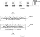
- Figure 7 shows a flow chart of a method for packaging a semiconductor detector.
- the semiconductor detector comprises: a cathode circuit board including a reading out chip; a cathode circuit board including a high voltage side top layer of the cathode circuit board, a bottom connection layer of the cathode circuit board and a dielectric which is filled between the high voltage side top layer of the cathode circuit board and the bottom connection layer of the cathode circuit board, the high voltage side top layer of the cathode circuit board being connected to the bottom connection layer of the cathode circuit board through a via hole; and a detector crystal including a crystal body, an anode and a cathode, the anode being connected to the reading out chip of the cathode circuit board.
- the method for packaging a semiconductor detect may comprises steps of: connecting the high voltage side top layer of the cathode circuit board to a high voltage input terminal of the semiconductor detector S701); and connecting the cathode to the cathode circuit board by directly contacting the bottom connection layer of the cathode circuit board with the cathode of the detector crystal (S702).
- a filter circuit is provided on the high voltage side top layer of the cathode circuit board to implement a filtering of the high voltage.
- the high voltage end of the detector crystal may be mechanically protected to reduce safety danger caused by the high voltage and to improve the stability of the high voltage connection; by adding the filter circuit at the nearest place to the detector, the noise caused by the high voltage may be effectively decreased to improve the performance of the detector; and by adjusting the size of the cathode and the anode circuit board, a seamless cascade of multiple detectors may be implemented.
Landscapes
- Physics & Mathematics (AREA)
- Health & Medical Sciences (AREA)
- Life Sciences & Earth Sciences (AREA)
- General Physics & Mathematics (AREA)
- High Energy & Nuclear Physics (AREA)
- Molecular Biology (AREA)
- Spectroscopy & Molecular Physics (AREA)
- Engineering & Computer Science (AREA)
- Multimedia (AREA)
- Signal Processing (AREA)
- Measurement Of Radiation (AREA)
Abstract
Description
- This application claims priority of Chinese Application No
201610797744.x filed at August 31, 2016 - The present disclosure relates to a semiconductor detector, and more particularly to a tellurium-zinc-cadmium semiconductor detector and a method for packaging the same, and more particularly to a cathode package, a high-voltage connection, a high-voltage filter for a semiconductor detector and an obtained semiconductor detector.
- Semiconductor detectors have been widely concerned with their high detection efficiency and better energy resolution, and are applied to various applications of radiation detection such as nuclide recognizers, metering alarms, etc. in environmental radiation detection, item detection such as goods machine, industrial CT (Computed Tomography) in national security field, CT, dental imaging, PET (Positron Emission Tomography), SPECT (Single Photon Emission Computed Tomography) and so on in medical applications. There are many types of semiconductor materials, such as CdMnTe (cadmium manganese telluride), Hgl2 (mercury iodide), TIBr (thallium bromide), Pbl2 (lead iodide), GaAs (gallium arsenide), Ge (germanium) or the like, which have different characteristics and are applied to different fields.
- Cadmium Zinc Telluride (CZT) crystal is one kind of excellent semiconductor radiation detection material at room temperature which is developed in recent years. CZT has a high resistivity, a large atomic number, and a large forbidden band width, so detector fabricated by CZT has a small leakage current and a better energy resolution for X and γ-ray at room temperature without polarization phenomenon. When the ray is incident into the detector, it interacts with CZT to generate electrons and holes. The electrons and holes are pulled in the electric field to move towards the anode and the cathode, respectively, to generate induction signals.
- In addition to its excellent energy resolution and high detection efficiency, CdZnTe works at room temperature, which is the most potential material for radiation detection. However, CZT is an expensive and fragile semiconductor material. In the existing design, the cathode are connected to high voltage wires by means of soldering or conductive adhesives, and the high voltage wires and electrodes are exposed to air. In this way, the crystal cathode surface and the high voltage connection line may be touched during installation, resulting in that the cathode surface becomes dirty and the high voltage wire is touched. Furthermore, mechanical contact will make the anode crystal broken, affect the detection performance of the crystal, and even damage the detector. The method of directly connecting the high-voltage wire to the cathode surface of the detector will bring security risks and lead to short circuit or space discharge; and the repeated installation will lead to high-voltage wire to be broken and damage the detector. In a situation where a number of detectors are integrated, the high-voltage side of the detector is far away from the high voltage source, which will increase a system noise since an effective filtering can't be implemented.
-
Figure 1 shows a high voltage connection of a cathode high voltage side of a traditional CZT. As shown infigure 1 , one terminal of thehigh voltage wire 101 is soldered to a cathode of adetector 102, and the other terminal of the high voltage wire is soldered to aPCB board 103 which is packaged with the anode; or the other terminal of the high voltage wire is directly connected to the high voltage source. For such a connection, it is not convenient to connect the high voltage wire, and a suspended wire will be deformed after a long time and is easy to touch the high voltage wire in use. Since the high voltage wire is connected to the PCB103 for the anode, the PCT for the anode is larger than the detector, it cannot implement seamless connection of multiple detectors. Since there is not any protecting means for the cathode, it is easy for the cathode to touch the detector in use, which leads to performance degradation. - The invention is defined in claims 1 and 11. The depended claims relate to preferred embodiments.
- The present invention provides a semiconductor detector and a packaging method thereof. The semiconductor detector comprises: a cathode circuit board including a reading out chip; a cathode circuit board including a high voltage side top layer of the cathode circuit board, a bottom connection layer of the cathode circuit board and a dielectric which is filled between the high voltage side top layer of the cathode circuit board and the bottom connection layer of the cathode circuit board; the high voltage side top layer of the cathode circuit board is connected to the bottom connection layer of the cathode circuit board through a via hole; and a detector crystal including a crystal body, an anode and a cathode, the anode is connected to the reading out chip of the cathode circuit board, the high voltage side top layer of the cathode circuit board is connected to an input terminal of the semiconductor detector and the bottom connection layer of the cathode circuit board directly contacts the cathode of the detector crystal to connect the cathode to the cathode circuit board.
- The present invention relates to a semiconductor detector, and more particularly to a tellurium-zinc-cadmium semiconductor detector and a method for packaging the same, and more particularly to a cathode package, a high-voltage connection, a high-voltage filter for a semiconductor detector and an obtained semiconductor detector.
- The present invention provides a semiconductor detector comprising: a cathode circuit board including a reading out chip; a cathode circuit board including a high voltage side top layer of the cathode circuit board, a bottom connection layer of the cathode circuit board and a dielectric which is filled between the high voltage side top layer of the cathode circuit board and the bottom connection layer of the cathode circuit board, the high voltage side top layer of the cathode circuit board being connected to the bottom connection layer of the cathode circuit board through a via hole; and a detector crystal including a crystal body, an anode and a cathode, the anode being connected to the reading out chip of the cathode circuit board, the high voltage side top layer of the cathode circuit board being connected to an input terminal of the semiconductor detector and the bottom connection layer of the cathode circuit board directly contacting the cathode of the detector crystal to connect the cathode to the cathode circuit board.
- The present invention also provides method for packing a semiconductor detector comprising: a cathode circuit board including a reading out chip; a cathode circuit board including a high voltage side top layer of the cathode circuit board, a bottom connection layer of the cathode circuit board and a dielectric which is filled between the high voltage side top layer of the cathode circuit board and the bottom connection layer of the cathode circuit board, the high voltage side top layer of the cathode circuit board being connected to the bottom connection layer of the cathode circuit board through a via hole; and a detector crystal including a crystal body, an anode and a cathode, the anode being connected to the reading out chip of the cathode circuit board, there method comprising: connecting the high voltage side top layer of the cathode circuit board to a high voltage input terminal of the semiconductor detector; and connecting the cathode to the cathode circuit board by directly contacting the bottom connection layer of the cathode circuit board with the cathode of the detector crystal.
- The method of the present invention may be applied to linear array detectors, pixel detectors and other semiconductor detectors.
- By means of the semiconductor detector and the method for packaging the same according to the present invention, the high voltage end of the detector crystal may be mechanically protected to reduce safety danger caused by the high voltage and to improve the stability of the high voltage connection. By adding the filter circuit at the nearest place to the detector, the noise caused by the high voltage may be effectively decreased to improve the performance of the detector; and by adjusting the size of the cathode and the anode circuit board, a seamless cascade of multiple detectors may be implemented.
- Reference will now be made to the embodiments of the present invention, examples of which are illustrated in the accompanying drawings, wherein like reference numerals refer to similar elements throughout the drawings. The following examples of the present invention will be described with reference to the accompanying drawings. In the drawings:
-
Figure 1 shows the high-voltage connection of a traditional CZT cathode high-voltage terminal; -
Figure 2 shows a side view of a PCB and a detector according to an embodiment of the present invention; -
Figure 3 shows a block diagram of a PCB according to an embodiment of the present invention; -
Figure 4 shows a bottom structure diagram of the PCB according to an embodiment of the present invention; -
Figure 5 shows a schematic view (top view) of a cascade structure of a plurality of detectors according to the present invention; -
Figure 6 shows a schematic view of providing a high voltage for multiple cascade modules through a flexible PCB; and -
Figure 7 shows a flow chart of a method for packaging a semiconductor detector. - The present invention directly packages a PCB (Printed Circuit Board) to a high voltage surface of a detector. At a high voltage connection terminal of the detector, the PCB board is directly packaged to the high voltage side of the detector. The type of electrode at the high voltage terminal may be a variety of shapes such as a plan array, pixels, strip and so on. The PCB board utilizes a double-layer structure of top and bottom layers, which is not limited to two layers. The bottom surface is an exposed electrode, which is directly packaged with a high-voltage electrode of the detector. The top surface of the PCB board is a high voltage connection surface and a filter circuit may be added at this top surface. A high voltage is connected to the top layer of the PCB board through wires, and is filtered in the top surface to be connected to a ground of the PCB through a via hole, which may effectively prevent an anode of the detector from contacting external environment and play a good effect of protection.
- The size of the PCB may be the same as that of the crystal, or it may be larger or smaller than that of the high voltage side of the detector. The shape of the crystal may be a rectangular shape, a square shape or a cylinder. Preferably, the PCB has the same shape and size as those of the detector.
- The present invention implements a connection of the high voltage source and the high voltage electrode of the detector through the PCB board. The PCB utilizes a double-layer structure (bottom layer and top layer), and may also utilizes a multi-layer PCB structure. The top and bottom layers of the PCB are connected through via holes, and the number of via holes is not limited and the distribution is also not limited. Preferably, the pluralities of via holes are distributed in many orientations so that the high voltage at the cathode surface of the detector may be uniformly distributed. The bottom electrode of the PCB is directly connected to the high voltage side of the detector by conductive adhesives or other means. The top layer of the PCB board utilizes solder patch socket, and a high-voltage connection may be made by plugging in and out a high voltage wire or direct soldering to implement the connection with the high voltage source. During such a process, it is preferable to use a flexible PCB board. The metal at soldering points may be as few as possible to reduce influence of the metal on top of the PCB board on the detector.
- The present invention may implement filtering of the high voltage by adding a filter circuit on the PCB at the high voltage side, which may reduce the distance between the filter circuit and the anode. The filter circuit for filtering the high-voltage utilizes an active filtering or a passive filtering, and preferably utilizes the passive filtering. The passive filtering may reduce the distance from the filtered high voltage to the detector, and may reduce the influence caused by the long wires which may affect detection performance of the detector. When the flexible PCB is utilized to implement connection of the PCB and the high voltage source, the filter circuit is preferably placed on the flexible PCB, and the passive filtering is preferred. In this way, the distance between the filtered high voltage and the detector is reduced. The shielding of the electronic components of the filter to the rays is decreased when the rays is incident at the cathode. When the ray is incident at the anode, the influence of the electronic components may be ignored.
- In the embodiment of the present invention, the CZT detector is used as an example, and the size of the detector is 10*10*10 mm3. The anode of the detector is a pixel structure, which is packaged on the PCT to be connected to the readout chip. The cathode of the detector is a planar structure, and is connected to a negative high voltage. The present invention is not limited by the electrode structure of the anode, the packaging mode or the like. The present invention is not limited by the electrode structure of the cathode, and the cathode electrode may be a planar array, a coplanar gate, a linear array and the like. The present invention is not limited by the shape of the detector, and the shape may be cuboids, cubes, cylinders and the like. The present invention is also not limited by the material of the detector.
- The present invention utilizes a means of directly packaging the PCB and the cathode of the detector, which protects the detector and also provides an effective high-voltage connection way. The PCB may also utilize a variety of materials.
- In an embodiment, the CZT detector has a shape of a cube.
Figure 2 shows a side view of the PCB and the detector according to an embodiment of the present invention. As shown infigure 2 , drawings of A, B and C infigure 2 show side views of the device according to the present invention in three cases, respectively, in which acomponent 201 is a PCB at the high voltage side (cathode), acomponent 202 is a detector crystal, and acomponent 203 is a circuit board at the other side (anode) of the crystal. The shape and size of the PCB at the cathode side are arbitrary, that is, the shape of thecomponent 201 may be a cylinder or a cuboid, and may be the same as or different from that of the cathode surface of the detector. The cathode and anode electrodes of thedetector 202 are not marked. -
Figure 3 shows a block diagram of a PCB according to an embodiment of the present invention. Such a package structure may effectively protect the anode of the detector, and may also implement a connection of the high voltage and the cathode of the detector through the PCB. As a result of utilizing the PCB board, the cathode of the detector may be directly connected through the bottom layer of the PCB board, and the high voltage may be connected to the top layer of the PCB board through via holes. Specifically, the PCB board structure is shown infigure 3 , in which acomponent 201 is a PCB board for detecting the high voltage side; acomponent 306 is a bottom layer of the PCB, a conductive material for bottom layer of the PCB (the material may be selected from, copper, etc.) may directly contact the cathode of the detector and may be connected by conductive adhesives; acomponent 305 is a top layer of the PCB which is connected to the high voltage; and acomponent 304 is the via hole which connects the bottom layer and the top layer. The number and distribution of viaholes 304 are not limited. Preferably, there may be a plurality of via holes distributed at a variety of positions. - The semiconductor detector according to an embodiment of the present invention comprises: a cathode circuit board including a reading out chip; a cathode circuit board including a high voltage side top layer of the cathode circuit board, a bottom connection layer of the cathode circuit board and a dielectric which is filled between the high voltage side top layer of the cathode circuit board and the bottom connection layer of the cathode circuit board, the high voltage side top layer of the cathode circuit board being connected to the bottom connection layer of the cathode circuit board through a via hole; and a detector crystal including a crystal body, an anode and a cathode, the anode being connected to the reading out chip of the cathode circuit board, the high voltage side top layer of the cathode circuit board being connected to an input terminal of the semiconductor detector and the bottom connection layer of the cathode circuit board directly contacting the cathode of the detector crystal to connect the cathode to the cathode circuit board.
- Preferably, the detector crystal is a tellurium-zinc-cadmium crystal.
- Preferably, the bottom connection layer of the cathode circuit board may contact the cathode by conductive adhesives.
- Preferably, the semiconductor detector comprises pluralities of via holes which are evenly arranged.
- Preferably, the high voltage side top layer of the cathode circuit board is connected to an external high voltage source through a solder patch socket or a direct soldering.
-
Figure 4 shows a bottom structure diagram of the PCB according to an embodiment of the present invention. In particular, abottom layer 305 of the PCB includes an opening for a viahole 304, afilter circuit 406, and aport 407. Theport 407 may be soldered or may be connected by away of a socket. Theport 407 may be directly connected to a high-voltage source, or may be connected for a cascade of multiple modules. Wires for cascade may use ordinary high-voltage wires, and may also use flexible PCBs. Preferably, the flexible PCT is used. The cascade may be a cascade of line arrays or a cascade of pixels to improve areas of the detector. - As shown in
Fig. 4 , in the semiconductor detector according to an embodiment of the present invention, a filter circuit is provided in the top layer of the high voltage side of the cathode circuit board. The filter circuit may utilize an active filtering or a passive filtering, and preferably utilizes the passive filtering. The passive filtering may reduce numbers of the elements in the filtering circuit, and may reduce the influence of heat generated by electronic devices on the performance of the detector. When elements of the passive filter circuit are selected, it needs to consider factors such as thermal dissipation, power consumption, materials and so on. That is to say, it needs to avoid influence on the performance of the detector and avoids excessive shielding of radiations. - The filter circuit is provided at edges of the top layer of the high voltage terminal of the cathode circuit board. By setting the high-voltage filter circuit to be the shortest distance from the anode of the detector, the influence of noise is decreased and the signal-to-noise ratio is improved. Such a way may improve an energy resolution of the detector.
- Preferably, the cathode circuit board is a flexible circuit board. The filter circuit is provided in the flexible circuit board. In other words, the filtering method may filter in the flexible PC. That is to say, the high voltage source and the top layer 405 of the PCB are connected through the flexible PCT and the filter circuit is placed at a position which is the closest to a
voltage connection port 407. Similarly, the filtering method may utilize an active filtering and a passive filter. The passive filtering is preferred. The passive filtering may reduce numbers of the elements in the filtering circuit, and may reduce the influence of heat generated by electronic devices on the performance of the detector. In this way, the shielding of the electronic components of the filter to the rays is decreased, and when the ray is incident at the anode, the shielding of the filter components to the radiations may be ignored. -
Figure 5 shows a schematic view (top view) of a cascade structure of a plurality of detectors according to the present invention. As shown infigure 5 , the present invention enables a cascade of multiple detector modules. In the prior art, the high voltage wire is connected with the cathode of the detector and then is leaded through the circuit board at the anode side of the detector, which can't implement the cascade of the plane array and there are a large gap between the cascaded detector modules. In the previous cascaded structure, the high voltage is only filtered once and then all of the detector modules are connected together. Due to lengthening of the high voltage wire, the system noise may be greatly increased. At the same time, the exposure of the high-voltage wire will bring security risks. By utilizing the cascaded structure as shown infigure 5 , a variety of cascades of the semiconductor detectors may be implemented. -
Figure 6 shows a schematic view of providing a high voltage for multiple cascade modules through a flexible PCB. As shown infigure 6 , when a flexible PCB is selected as a high-voltage connection line, a width of the flexible PCB may be increased. In this case, the filter circuit may be placed on the flexible PCB to be close to ports of the PCB board for the cathode. An arrangement of the flexible PCB layout should evade the top of the detector at the edge of the detector, thereby reducing shielding of the radiations. The shape of the flexible PCB according to the present invention is not limited, and the flexible PCBs may utilize a flexible PCB with other shapes and structures. -
Figure 7 shows a flow chart of a method for packaging a semiconductor detector. The semiconductor detector comprises: a cathode circuit board including a reading out chip; a cathode circuit board including a high voltage side top layer of the cathode circuit board, a bottom connection layer of the cathode circuit board and a dielectric which is filled between the high voltage side top layer of the cathode circuit board and the bottom connection layer of the cathode circuit board, the high voltage side top layer of the cathode circuit board being connected to the bottom connection layer of the cathode circuit board through a via hole; and a detector crystal including a crystal body, an anode and a cathode, the anode being connected to the reading out chip of the cathode circuit board. The method for packaging a semiconductor detect may comprises steps of: connecting the high voltage side top layer of the cathode circuit board to a high voltage input terminal of the semiconductor detector S701); and connecting the cathode to the cathode circuit board by directly contacting the bottom connection layer of the cathode circuit board with the cathode of the detector crystal (S702). - In particular, a filter circuit is provided on the high voltage side top layer of the cathode circuit board to implement a filtering of the high voltage.
- By means of the semiconductor detector and the method for packaging the same according to the present invention, the high voltage end of the detector crystal may be mechanically protected to reduce safety danger caused by the high voltage and to improve the stability of the high voltage connection; by adding the filter circuit at the nearest place to the detector, the noise caused by the high voltage may be effectively decreased to improve the performance of the detector; and by adjusting the size of the cathode and the anode circuit board, a seamless cascade of multiple detectors may be implemented.
- Although the present invention has been particularly shown and described with reference to exemplary embodiments thereof, it will be understood by those skilled in the art that various changes and modifications in form and detail may be made without departing from the scope of the invention as defined by the appended claims.
Claims (12)
- A semiconductor detector comprising:- a cathode circuit board including a reading out chip;- a cathode circuit board including a high voltage side top layer of the cathode circuit board, a bottom connection layer of the cathode circuit board and a dielectric which is filled between the high voltage side top layer of the cathode circuit board and the bottom connection layer of the cathode circuit board, the high voltage side top layer of the cathode circuit board being connected to the bottom connection layer of the cathode circuit board through a via hole; and- a detector crystal including a crystal body, an anode and a cathode, the anode being connected to the reading out chip of the cathode circuit board,- wherein the high voltage side top layer of the cathode circuit board being connected to an input terminal of the semiconductor detector and the bottom connection layer of the cathode circuit board directly contacting the cathode of the detector crystal to connect the cathode to the cathode circuit board.
- The semiconductor detector according to claim 1, wherein the detector crystal is a tellurium-zinc-cadmium crystal.
- The semiconductor detector according to claim 1 or 2, wherein the bottom connection layer of the cathode circuit board contacts the cathode by conductive adhesives.
- The semiconductor detector according to claim 1, 2 or 3, wherein a filter circuit is provided in the high voltage side top layer of the cathode circuit board.
- The semiconductor detector according to claim 4, wherein the filter circuit utilizes a passive filtering.
- The semiconductor detector according to claim 4 or 5, wherein the filter circuit is provided at an edge region of the high voltage side top layer of the cathode circuit board.
- The semiconductor detector according to any of the above claims, comprising pluralities of via holes which are evenly arranged.
- The semiconductor detector according to any of the above claims, wherein the high voltage side top layer of the cathode circuit board is connected to an external high voltage source through a solder patch socket or by a direct soldering.
- The semiconductor detector according to any of the above claims, wherein the cathode circuit board is a flexible circuit board.
- The semiconductor detector according to claim 9, wherein the filter circuit is provided in the flexible circuit board.
- A method for packing a semiconductor detector, the semiconductor detector comprising:- a cathode circuit board including a reading out chip;- a cathode circuit board including a high voltage side top layer of the cathode circuit board, a bottom connection layer of the cathode circuit board and a dielectric which is filled between the high voltage side top layer of the cathode circuit board and the bottom connection layer of the cathode circuit board, the high voltage side top layer of the cathode circuit board being connected to the bottom connection layer of the cathode circuit board through a via hole; and- a detector crystal including a crystal body, an anode and a cathode, the anode being connected to the reading out chip of the cathode circuit board,- the method comprising steps of: connecting the high voltage side top layer of the cathode circuit board to a high voltage input terminal of the semiconductor detector; and connecting the cathode to the cathode circuit board by directly contacting the bottom connection layer of the cathode circuit board with the cathode of the detector crystal.
- The method according to claim 11, wherein a filter circuit is provided in the high voltage side top layer of the cathode circuit board to filter a high voltage.
Applications Claiming Priority (1)
| Application Number | Priority Date | Filing Date | Title |
|---|---|---|---|
| CN201610797744.XA CN106324648B (en) | 2016-08-31 | 2016-08-31 | Semiconductor detector and packaging method thereof |
Publications (2)
| Publication Number | Publication Date |
|---|---|
| EP3290955A1 true EP3290955A1 (en) | 2018-03-07 |
| EP3290955B1 EP3290955B1 (en) | 2020-07-01 |
Family
ID=57787168
Family Applications (1)
| Application Number | Title | Priority Date | Filing Date |
|---|---|---|---|
| EP17173053.4A Active EP3290955B1 (en) | 2016-08-31 | 2017-05-26 | Semiconductor detector and method for packaging the same |
Country Status (3)
| Country | Link |
|---|---|
| US (1) | US10670743B2 (en) |
| EP (1) | EP3290955B1 (en) |
| CN (2) | CN106324648B (en) |
Families Citing this family (3)
| Publication number | Priority date | Publication date | Assignee | Title |
|---|---|---|---|---|
| US10910432B1 (en) * | 2019-07-23 | 2021-02-02 | Cyber Medical Imaging, Inc. | Use of surface patterning for fabricating a single die direct capture dental X-ray imaging sensor |
| CN111372437B (en) * | 2020-04-17 | 2021-07-06 | 深圳市欧盛自动化有限公司 | Rubber shell mounting machine and automatic production device of circuit board thereof |
| CN118431306A (en) * | 2024-07-04 | 2024-08-02 | 陕西迪泰克新材料有限公司 | Tellurium-zinc-cadmium radiation detection chip and cathode packaging method thereof |
Citations (4)
| Publication number | Priority date | Publication date | Assignee | Title |
|---|---|---|---|---|
| EP1492168A1 (en) * | 2002-03-08 | 2004-12-29 | Hamamatsu Photonics K.K. | Sensor |
| US20080149844A1 (en) * | 2006-12-21 | 2008-06-26 | Redlen Technologies | Use of solder mask as a protective coating for radiation detector |
| US20110272589A1 (en) * | 2010-05-03 | 2011-11-10 | Brookhaven Science Associates, Llc | Hybrid Anode for Semiconductor Radiation Detectors |
| WO2016046014A1 (en) * | 2014-09-26 | 2016-03-31 | Koninklijke Philips N.V. | Radiation detector with heating device |
Family Cites Families (6)
| Publication number | Priority date | Publication date | Assignee | Title |
|---|---|---|---|---|
| US7227150B2 (en) * | 2004-05-04 | 2007-06-05 | General Electric Co. | Solid-state x-ray detector with support mounted steering electrodes |
| US7606347B2 (en) * | 2004-09-13 | 2009-10-20 | General Electric Company | Photon counting x-ray detector with overrange logic control |
| US7525098B2 (en) * | 2006-04-05 | 2009-04-28 | Orbotech Ltd. | High resolution energy detector |
| JP5032276B2 (en) * | 2007-11-19 | 2012-09-26 | 株式会社東芝 | Radiation detector |
| JP5588190B2 (en) * | 2010-02-08 | 2014-09-10 | 日立アロカメディカル株式会社 | Radiation detection module |
| CN206147105U (en) * | 2016-08-31 | 2017-05-03 | 同方威视技术股份有限公司 | semiconductor detector |
-
2016
- 2016-08-31 CN CN201610797744.XA patent/CN106324648B/en active Active
- 2016-08-31 CN CN202311044144.2A patent/CN117075174A/en active Pending
-
2017
- 2017-05-26 EP EP17173053.4A patent/EP3290955B1/en active Active
- 2017-05-26 US US15/606,394 patent/US10670743B2/en not_active Expired - Fee Related
Patent Citations (4)
| Publication number | Priority date | Publication date | Assignee | Title |
|---|---|---|---|---|
| EP1492168A1 (en) * | 2002-03-08 | 2004-12-29 | Hamamatsu Photonics K.K. | Sensor |
| US20080149844A1 (en) * | 2006-12-21 | 2008-06-26 | Redlen Technologies | Use of solder mask as a protective coating for radiation detector |
| US20110272589A1 (en) * | 2010-05-03 | 2011-11-10 | Brookhaven Science Associates, Llc | Hybrid Anode for Semiconductor Radiation Detectors |
| WO2016046014A1 (en) * | 2014-09-26 | 2016-03-31 | Koninklijke Philips N.V. | Radiation detector with heating device |
Also Published As
| Publication number | Publication date |
|---|---|
| EP3290955B1 (en) | 2020-07-01 |
| CN106324648B (en) | 2023-08-01 |
| CN117075174A (en) | 2023-11-17 |
| CN106324648A (en) | 2017-01-11 |
| US20180059265A1 (en) | 2018-03-01 |
| US10670743B2 (en) | 2020-06-02 |
Similar Documents
| Publication | Publication Date | Title |
|---|---|---|
| EP2560027B1 (en) | Connection substrate | |
| EP2560026B1 (en) | Radiation detector module | |
| CN106324649B (en) | semiconductor detector | |
| JP2008510130A5 (en) | ||
| EP3290955B1 (en) | Semiconductor detector and method for packaging the same | |
| JP2019504295A (en) | Radiation detector and imaging device | |
| US20210202557A1 (en) | Radiation-resistant image sensor package | |
| US10502842B2 (en) | Radiation detector | |
| WO2008108995A1 (en) | Electric field steering cap, steering electrode, and modular configurations for a radiation detector | |
| US12019193B2 (en) | Imaging system | |
| CN206147105U (en) | semiconductor detector | |
| US20230280482A1 (en) | Imaging systems | |
| CN112928106B (en) | Detector device and array panel | |
| CN204556842U (en) | Linear array detector | |
| US11984407B2 (en) | Package structure and communications device with suppressed ion migration in bonding material | |
| EP3291311B1 (en) | Semiconductor detector | |
| JP6241066B2 (en) | Radiation imaging equipment | |
| JP2007155565A (en) | Radiation image detection module | |
| CN206074817U (en) | Semiconductor detector | |
| JP4641211B2 (en) | Radiation detector and radiation inspection apparatus | |
| US20210159192A1 (en) | Lead Frame for Multi-Chip Modules With Integrated Surge Protection | |
| CN120240008A (en) | Arrangement of radiation detectors in image sensors | |
| JP2025160607A (en) | Radiation detector and radiation detection device |
Legal Events
| Date | Code | Title | Description |
|---|---|---|---|
| PUAI | Public reference made under article 153(3) epc to a published international application that has entered the european phase |
Free format text: ORIGINAL CODE: 0009012 |
|
| STAA | Information on the status of an ep patent application or granted ep patent |
Free format text: STATUS: REQUEST FOR EXAMINATION WAS MADE |
|
| 17P | Request for examination filed |
Effective date: 20170624 |
|
| AK | Designated contracting states |
Kind code of ref document: A1 Designated state(s): AL AT BE BG CH CY CZ DE DK EE ES FI FR GB GR HR HU IE IS IT LI LT LU LV MC MK MT NL NO PL PT RO RS SE SI SK SM TR |
|
| AX | Request for extension of the european patent |
Extension state: BA ME |
|
| GRAP | Despatch of communication of intention to grant a patent |
Free format text: ORIGINAL CODE: EPIDOSNIGR1 |
|
| STAA | Information on the status of an ep patent application or granted ep patent |
Free format text: STATUS: GRANT OF PATENT IS INTENDED |
|
| INTG | Intention to grant announced |
Effective date: 20200205 |
|
| RIN1 | Information on inventor provided before grant (corrected) |
Inventor name: XU, GUANGMING Inventor name: CAO, XUEPENG Inventor name: LI, JUN Inventor name: ZHANG, LAN Inventor name: HU, HAIFAN Inventor name: GU, JIANPING Inventor name: DU, YINGSHUAI Inventor name: WU, ZONGGUI Inventor name: LI, BO Inventor name: LIU, BICHENG |
|
| GRAS | Grant fee paid |
Free format text: ORIGINAL CODE: EPIDOSNIGR3 |
|
| GRAA | (expected) grant |
Free format text: ORIGINAL CODE: 0009210 |
|
| STAA | Information on the status of an ep patent application or granted ep patent |
Free format text: STATUS: THE PATENT HAS BEEN GRANTED |
|
| AK | Designated contracting states |
Kind code of ref document: B1 Designated state(s): AL AT BE BG CH CY CZ DE DK EE ES FI FR GB GR HR HU IE IS IT LI LT LU LV MC MK MT NL NO PL PT RO RS SE SI SK SM TR |
|
| REG | Reference to a national code |
Ref country code: CH Ref legal event code: EP Ref country code: AT Ref legal event code: REF Ref document number: 1286679 Country of ref document: AT Kind code of ref document: T Effective date: 20200715 |
|
| REG | Reference to a national code |
Ref country code: IE Ref legal event code: FG4D |
|
| REG | Reference to a national code |
Ref country code: DE Ref legal event code: R096 Ref document number: 602017018902 Country of ref document: DE |
|
| REG | Reference to a national code |
Ref country code: FI Ref legal event code: FGE |
|
| REG | Reference to a national code |
Ref country code: LT Ref legal event code: MG4D |
|
| PG25 | Lapsed in a contracting state [announced via postgrant information from national office to epo] |
Ref country code: BG Free format text: LAPSE BECAUSE OF FAILURE TO SUBMIT A TRANSLATION OF THE DESCRIPTION OR TO PAY THE FEE WITHIN THE PRESCRIBED TIME-LIMIT Effective date: 20201001 |
|
| REG | Reference to a national code |
Ref country code: NL Ref legal event code: MP Effective date: 20200701 |
|
| REG | Reference to a national code |
Ref country code: AT Ref legal event code: MK05 Ref document number: 1286679 Country of ref document: AT Kind code of ref document: T Effective date: 20200701 |
|
| PG25 | Lapsed in a contracting state [announced via postgrant information from national office to epo] |
Ref country code: HR Free format text: LAPSE BECAUSE OF FAILURE TO SUBMIT A TRANSLATION OF THE DESCRIPTION OR TO PAY THE FEE WITHIN THE PRESCRIBED TIME-LIMIT Effective date: 20200701 Ref country code: SE Free format text: LAPSE BECAUSE OF FAILURE TO SUBMIT A TRANSLATION OF THE DESCRIPTION OR TO PAY THE FEE WITHIN THE PRESCRIBED TIME-LIMIT Effective date: 20200701 Ref country code: GR Free format text: LAPSE BECAUSE OF FAILURE TO SUBMIT A TRANSLATION OF THE DESCRIPTION OR TO PAY THE FEE WITHIN THE PRESCRIBED TIME-LIMIT Effective date: 20201002 Ref country code: NO Free format text: LAPSE BECAUSE OF FAILURE TO SUBMIT A TRANSLATION OF THE DESCRIPTION OR TO PAY THE FEE WITHIN THE PRESCRIBED TIME-LIMIT Effective date: 20201001 Ref country code: ES Free format text: LAPSE BECAUSE OF FAILURE TO SUBMIT A TRANSLATION OF THE DESCRIPTION OR TO PAY THE FEE WITHIN THE PRESCRIBED TIME-LIMIT Effective date: 20200701 Ref country code: AT Free format text: LAPSE BECAUSE OF FAILURE TO SUBMIT A TRANSLATION OF THE DESCRIPTION OR TO PAY THE FEE WITHIN THE PRESCRIBED TIME-LIMIT Effective date: 20200701 Ref country code: LT Free format text: LAPSE BECAUSE OF FAILURE TO SUBMIT A TRANSLATION OF THE DESCRIPTION OR TO PAY THE FEE WITHIN THE PRESCRIBED TIME-LIMIT Effective date: 20200701 Ref country code: PT Free format text: LAPSE BECAUSE OF FAILURE TO SUBMIT A TRANSLATION OF THE DESCRIPTION OR TO PAY THE FEE WITHIN THE PRESCRIBED TIME-LIMIT Effective date: 20201102 Ref country code: CZ Free format text: LAPSE BECAUSE OF FAILURE TO SUBMIT A TRANSLATION OF THE DESCRIPTION OR TO PAY THE FEE WITHIN THE PRESCRIBED TIME-LIMIT Effective date: 20200701 |
|
| PG25 | Lapsed in a contracting state [announced via postgrant information from national office to epo] |
Ref country code: PL Free format text: LAPSE BECAUSE OF FAILURE TO SUBMIT A TRANSLATION OF THE DESCRIPTION OR TO PAY THE FEE WITHIN THE PRESCRIBED TIME-LIMIT Effective date: 20200701 Ref country code: LV Free format text: LAPSE BECAUSE OF FAILURE TO SUBMIT A TRANSLATION OF THE DESCRIPTION OR TO PAY THE FEE WITHIN THE PRESCRIBED TIME-LIMIT Effective date: 20200701 Ref country code: RS Free format text: LAPSE BECAUSE OF FAILURE TO SUBMIT A TRANSLATION OF THE DESCRIPTION OR TO PAY THE FEE WITHIN THE PRESCRIBED TIME-LIMIT Effective date: 20200701 Ref country code: IS Free format text: LAPSE BECAUSE OF FAILURE TO SUBMIT A TRANSLATION OF THE DESCRIPTION OR TO PAY THE FEE WITHIN THE PRESCRIBED TIME-LIMIT Effective date: 20201101 |
|
| PG25 | Lapsed in a contracting state [announced via postgrant information from national office to epo] |
Ref country code: NL Free format text: LAPSE BECAUSE OF FAILURE TO SUBMIT A TRANSLATION OF THE DESCRIPTION OR TO PAY THE FEE WITHIN THE PRESCRIBED TIME-LIMIT Effective date: 20200701 |
|
| REG | Reference to a national code |
Ref country code: DE Ref legal event code: R097 Ref document number: 602017018902 Country of ref document: DE |
|
| PG25 | Lapsed in a contracting state [announced via postgrant information from national office to epo] |
Ref country code: RO Free format text: LAPSE BECAUSE OF FAILURE TO SUBMIT A TRANSLATION OF THE DESCRIPTION OR TO PAY THE FEE WITHIN THE PRESCRIBED TIME-LIMIT Effective date: 20200701 Ref country code: DK Free format text: LAPSE BECAUSE OF FAILURE TO SUBMIT A TRANSLATION OF THE DESCRIPTION OR TO PAY THE FEE WITHIN THE PRESCRIBED TIME-LIMIT Effective date: 20200701 Ref country code: EE Free format text: LAPSE BECAUSE OF FAILURE TO SUBMIT A TRANSLATION OF THE DESCRIPTION OR TO PAY THE FEE WITHIN THE PRESCRIBED TIME-LIMIT Effective date: 20200701 Ref country code: IT Free format text: LAPSE BECAUSE OF FAILURE TO SUBMIT A TRANSLATION OF THE DESCRIPTION OR TO PAY THE FEE WITHIN THE PRESCRIBED TIME-LIMIT Effective date: 20200701 Ref country code: SM Free format text: LAPSE BECAUSE OF FAILURE TO SUBMIT A TRANSLATION OF THE DESCRIPTION OR TO PAY THE FEE WITHIN THE PRESCRIBED TIME-LIMIT Effective date: 20200701 |
|
| PLBE | No opposition filed within time limit |
Free format text: ORIGINAL CODE: 0009261 |
|
| STAA | Information on the status of an ep patent application or granted ep patent |
Free format text: STATUS: NO OPPOSITION FILED WITHIN TIME LIMIT |
|
| PG25 | Lapsed in a contracting state [announced via postgrant information from national office to epo] |
Ref country code: AL Free format text: LAPSE BECAUSE OF FAILURE TO SUBMIT A TRANSLATION OF THE DESCRIPTION OR TO PAY THE FEE WITHIN THE PRESCRIBED TIME-LIMIT Effective date: 20200701 |
|
| 26N | No opposition filed |
Effective date: 20210406 |
|
| PG25 | Lapsed in a contracting state [announced via postgrant information from national office to epo] |
Ref country code: SK Free format text: LAPSE BECAUSE OF FAILURE TO SUBMIT A TRANSLATION OF THE DESCRIPTION OR TO PAY THE FEE WITHIN THE PRESCRIBED TIME-LIMIT Effective date: 20200701 |
|
| PG25 | Lapsed in a contracting state [announced via postgrant information from national office to epo] |
Ref country code: SI Free format text: LAPSE BECAUSE OF FAILURE TO SUBMIT A TRANSLATION OF THE DESCRIPTION OR TO PAY THE FEE WITHIN THE PRESCRIBED TIME-LIMIT Effective date: 20200701 |
|
| REG | Reference to a national code |
Ref country code: DE Ref legal event code: R119 Ref document number: 602017018902 Country of ref document: DE |
|
| PG25 | Lapsed in a contracting state [announced via postgrant information from national office to epo] |
Ref country code: MC Free format text: LAPSE BECAUSE OF FAILURE TO SUBMIT A TRANSLATION OF THE DESCRIPTION OR TO PAY THE FEE WITHIN THE PRESCRIBED TIME-LIMIT Effective date: 20200701 Ref country code: LU Free format text: LAPSE BECAUSE OF NON-PAYMENT OF DUE FEES Effective date: 20210526 |
|
| REG | Reference to a national code |
Ref country code: BE Ref legal event code: MM Effective date: 20210531 |
|
| PG25 | Lapsed in a contracting state [announced via postgrant information from national office to epo] |
Ref country code: IE Free format text: LAPSE BECAUSE OF NON-PAYMENT OF DUE FEES Effective date: 20210526 Ref country code: DE Free format text: LAPSE BECAUSE OF NON-PAYMENT OF DUE FEES Effective date: 20211201 |
|
| PG25 | Lapsed in a contracting state [announced via postgrant information from national office to epo] |
Ref country code: FR Free format text: LAPSE BECAUSE OF NON-PAYMENT OF DUE FEES Effective date: 20210531 |
|
| PG25 | Lapsed in a contracting state [announced via postgrant information from national office to epo] |
Ref country code: BE Free format text: LAPSE BECAUSE OF NON-PAYMENT OF DUE FEES Effective date: 20210531 |
|
| PG25 | Lapsed in a contracting state [announced via postgrant information from national office to epo] |
Ref country code: HU Free format text: LAPSE BECAUSE OF FAILURE TO SUBMIT A TRANSLATION OF THE DESCRIPTION OR TO PAY THE FEE WITHIN THE PRESCRIBED TIME-LIMIT; INVALID AB INITIO Effective date: 20170526 |
|
| PG25 | Lapsed in a contracting state [announced via postgrant information from national office to epo] |
Ref country code: CY Free format text: LAPSE BECAUSE OF FAILURE TO SUBMIT A TRANSLATION OF THE DESCRIPTION OR TO PAY THE FEE WITHIN THE PRESCRIBED TIME-LIMIT Effective date: 20200701 |
|
| P01 | Opt-out of the competence of the unified patent court (upc) registered |
Effective date: 20230528 |
|
| PG25 | Lapsed in a contracting state [announced via postgrant information from national office to epo] |
Ref country code: MK Free format text: LAPSE BECAUSE OF FAILURE TO SUBMIT A TRANSLATION OF THE DESCRIPTION OR TO PAY THE FEE WITHIN THE PRESCRIBED TIME-LIMIT Effective date: 20200701 |
|
| PG25 | Lapsed in a contracting state [announced via postgrant information from national office to epo] |
Ref country code: MT Free format text: LAPSE BECAUSE OF FAILURE TO SUBMIT A TRANSLATION OF THE DESCRIPTION OR TO PAY THE FEE WITHIN THE PRESCRIBED TIME-LIMIT Effective date: 20200701 |
|
| PG25 | Lapsed in a contracting state [announced via postgrant information from national office to epo] |
Ref country code: TR Free format text: LAPSE BECAUSE OF FAILURE TO SUBMIT A TRANSLATION OF THE DESCRIPTION OR TO PAY THE FEE WITHIN THE PRESCRIBED TIME-LIMIT Effective date: 20200701 |
|
| PGFP | Annual fee paid to national office [announced via postgrant information from national office to epo] |
Ref country code: GB Payment date: 20260325 Year of fee payment: 10 |
|
| REG | Reference to a national code |
Ref country code: CH Ref legal event code: U11 Free format text: ST27 STATUS EVENT CODE: U-0-0-U10-U11 (AS PROVIDED BY THE NATIONAL OFFICE) Effective date: 20260601 |
|
| PGFP | Annual fee paid to national office [announced via postgrant information from national office to epo] |
Ref country code: FI Payment date: 20260521 Year of fee payment: 10 |
|
| PGFP | Annual fee paid to national office [announced via postgrant information from national office to epo] |
Ref country code: CH Payment date: 20260601 Year of fee payment: 10 |