EP3290934A1 - Scan circuitry with iddq verification - Google Patents
Scan circuitry with iddq verification Download PDFInfo
- Publication number
- EP3290934A1 EP3290934A1 EP17185242.9A EP17185242A EP3290934A1 EP 3290934 A1 EP3290934 A1 EP 3290934A1 EP 17185242 A EP17185242 A EP 17185242A EP 3290934 A1 EP3290934 A1 EP 3290934A1
- Authority
- EP
- European Patent Office
- Prior art keywords
- logic
- node
- current
- power supply
- supply terminal
- Prior art date
- Legal status (The legal status is an assumption and is not a legal conclusion. Google has not performed a legal analysis and makes no representation as to the accuracy of the status listed.)
- Granted
Links
Images


Classifications
-
- G—PHYSICS
- G01—MEASURING; TESTING
- G01R—MEASURING ELECTRIC VARIABLES; MEASURING MAGNETIC VARIABLES
- G01R31/00—Arrangements for testing electric properties; Arrangements for locating electric faults; Arrangements for electrical testing characterised by what is being tested not provided for elsewhere
- G01R31/28—Testing of electronic circuits, e.g. by signal tracer
- G01R31/317—Testing of digital circuits
- G01R31/3177—Testing of logic operation, e.g. by logic analysers
-
- G—PHYSICS
- G01—MEASURING; TESTING
- G01R—MEASURING ELECTRIC VARIABLES; MEASURING MAGNETIC VARIABLES
- G01R31/00—Arrangements for testing electric properties; Arrangements for locating electric faults; Arrangements for electrical testing characterised by what is being tested not provided for elsewhere
- G01R31/28—Testing of electronic circuits, e.g. by signal tracer
- G01R31/30—Marginal testing, e.g. by varying supply voltage
- G01R31/3004—Current or voltage test
-
- G—PHYSICS
- G01—MEASURING; TESTING
- G01R—MEASURING ELECTRIC VARIABLES; MEASURING MAGNETIC VARIABLES
- G01R31/00—Arrangements for testing electric properties; Arrangements for locating electric faults; Arrangements for electrical testing characterised by what is being tested not provided for elsewhere
- G01R31/28—Testing of electronic circuits, e.g. by signal tracer
- G01R31/30—Marginal testing, e.g. by varying supply voltage
- G01R31/3004—Current or voltage test
- G01R31/3008—Quiescent current [IDDQ] test or leakage current test
-
- G—PHYSICS
- G01—MEASURING; TESTING
- G01R—MEASURING ELECTRIC VARIABLES; MEASURING MAGNETIC VARIABLES
- G01R31/00—Arrangements for testing electric properties; Arrangements for locating electric faults; Arrangements for electrical testing characterised by what is being tested not provided for elsewhere
- G01R31/28—Testing of electronic circuits, e.g. by signal tracer
- G01R31/30—Marginal testing, e.g. by varying supply voltage
- G01R31/3004—Current or voltage test
- G01R31/3012—Built-In-Current test [BIC]
-
- G—PHYSICS
- G01—MEASURING; TESTING
- G01R—MEASURING ELECTRIC VARIABLES; MEASURING MAGNETIC VARIABLES
- G01R31/00—Arrangements for testing electric properties; Arrangements for locating electric faults; Arrangements for electrical testing characterised by what is being tested not provided for elsewhere
- G01R31/28—Testing of electronic circuits, e.g. by signal tracer
- G01R31/317—Testing of digital circuits
- G01R31/31723—Hardware for routing the test signal within the device under test to the circuits to be tested, e.g. multiplexer for multiple core testing, accessing internal nodes
-
- G—PHYSICS
- G01—MEASURING; TESTING
- G01R—MEASURING ELECTRIC VARIABLES; MEASURING MAGNETIC VARIABLES
- G01R31/00—Arrangements for testing electric properties; Arrangements for locating electric faults; Arrangements for electrical testing characterised by what is being tested not provided for elsewhere
- G01R31/28—Testing of electronic circuits, e.g. by signal tracer
- G01R31/317—Testing of digital circuits
- G01R31/3181—Functional testing
- G01R31/3185—Reconfiguring for testing, e.g. LSSD, partitioning
- G01R31/318533—Reconfiguring for testing, e.g. LSSD, partitioning using scanning techniques, e.g. LSSD, Boundary Scan, JTAG
-
- G—PHYSICS
- G01—MEASURING; TESTING
- G01R—MEASURING ELECTRIC VARIABLES; MEASURING MAGNETIC VARIABLES
- G01R31/00—Arrangements for testing electric properties; Arrangements for locating electric faults; Arrangements for electrical testing characterised by what is being tested not provided for elsewhere
- G01R31/28—Testing of electronic circuits, e.g. by signal tracer
- G01R31/317—Testing of digital circuits
- G01R31/3181—Functional testing
- G01R31/3185—Reconfiguring for testing, e.g. LSSD, partitioning
- G01R31/318533—Reconfiguring for testing, e.g. LSSD, partitioning using scanning techniques, e.g. LSSD, Boundary Scan, JTAG
- G01R31/318575—Power distribution; Power saving
-
- G—PHYSICS
- G01—MEASURING; TESTING
- G01R—MEASURING ELECTRIC VARIABLES; MEASURING MAGNETIC VARIABLES
- G01R31/00—Arrangements for testing electric properties; Arrangements for locating electric faults; Arrangements for electrical testing characterised by what is being tested not provided for elsewhere
- G01R31/28—Testing of electronic circuits, e.g. by signal tracer
- G01R31/317—Testing of digital circuits
- G01R31/3181—Functional testing
- G01R31/3185—Reconfiguring for testing, e.g. LSSD, partitioning
- G01R31/318533—Reconfiguring for testing, e.g. LSSD, partitioning using scanning techniques, e.g. LSSD, Boundary Scan, JTAG
- G01R31/318577—AC testing, e.g. current testing, burn-in
Definitions
- the present invention relates generally to integrated circuits, and more particularly, to quiescent current (IDDQ) verification for scan test circuitry.
- IDDQ quiescent current
- Integrated circuits including system-on-chips (SoCs) integrate various digital and sometimes analog components on a single chip.
- ICs may have manufacturing defects such as physical failures and fabrication defects that cause the ICs to malfunction. Thus, the ICs need to be tested to detect manufacturing defects.
- Design for test (DFT) techniques add testability features to ICs that allow automatic test equipment (ATE) to execute various fault tests using test patterns generated by an automatic test pattern generator (ATPG) on the ICs to identify manufacturing defects.
- ATE automatic test equipment
- AVG automatic test pattern generator
- ICs that undergo fault testing include multiple scan flip-flops that form scan chains. Specific vectors of data are shifted in one end of each scan chain and results out the other end with the results compared with expectations to detect any faults. At each vector application, the IDDQ current consumed by the circuit may be measured and compared to predetermined limits. It is important to ensure that the IDDQ measurement circuitry and instruments are operating correctly.
- Vectors are a set of inputs designed to test a system. Various vectors can be used to test a system's behavior in response to various inputs. Scan testing has two components: one component for functional (logic) testing, and another component for IDDQ testing. The same chain (but different vectors) is used for each.
- An integrated circuit comprising: a first logic block coupled between a first power supply terminal and a second power supply terminal, wherein the first logic block includes: a first scan chain; and a configurable defect coupled to a scan output node of the first scan chain and having a logic node and a conductive element coupled between the logic node and the first or the second power supply terminal, wherein the configurable defect is configured to, during a quiescent current testing mode, place a predetermined logic state on the logic node such that a detectable current flows through the conductive element; a current measurement circuit configured to detect the detectable current when the integrated circuit is not defective.
- Embodiments of integrated circuits and methods are disclosed in which one or more verification vectors are added to a set of scan test vectors.
- a verification circuitry is added which consumes detectable additional current only when the verification vector(s) are configured by shifting the vectors into the scan chain.
- ATE automated test equipment
- IDDQ quiescent current
- the verification vectors and circuitry thus allow manufacturers and users to determine whether IDDQ failures exist, as well as to determine whether the ATE is configured correctly.
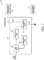
- FIG. 1 is a block diagram of a quiescent current verification system 100 in accordance with selected embodiments of the present invention including integrated circuitry 102 having scan chain 104, scan output node 106, combinational logic 108 and configurable defect 110.
- Configurable defect 110 is coupled between first voltage supply terminal VDD and second voltage supply terminal VSS (or ground).
- ATE with IDDQ current measurement circuitry 112, 114 can be coupled to first voltage supply terminal VDD at a first terminal of configurable defect 110.
- IDDQ current measurement circuitry 112, 114 may be coupled to the second voltage supply terminal VSS at a second terminal of configurable defect 110. Either way, IDDQ current measurement circuitry 112, 114 can detect whether configurable defect 110 is consuming current under the control of scan output node 106.
- Combinational logic 108 and scan chain 104 can be any integrated circuitry that is subject to scan test to verify proper operation, such as a processor, sensor, memory or other device composed of digital and/or analog electronic components.
- IDDQ current measurement circuitry 112, 114 along with corresponding scan chain(s) 104 and combinational logic 108 can be implemented in any suitable ATE system for electronic devices or systems.
- External test equipment provides one or more test vectors to scan chain 104.
- An output of scan chain 104 is provided to scan output node 106.
- Scan output node 106 is configured to provide input to configurable defect 110.
- configurable defect 110 consumes an additional detectable current from the voltage supply.
- the output from one latch circuitry is provided as data to the combinational logic 108 and as input to a subsequent latch circuit.
- the output of latch circuitry in scan chain 104 is provided as input to scan output node 106.
- Current through configurable defect 110 can be detected by IDDQ current measurement circuitry 112, 114.
- IDDQ current measurement circuitry 114 can be coupled to measure current at ground terminal 116 in addition to, or instead of IDDQ current measurement circuitry 112 that is coupled to supply voltage terminal VDD. IDDQ current measurement circuitry 112, 114 can determine whether current is being drawn by configurable defect 110, and whether the draw on current is expected given the output from scan chain 104. In general, at least one of the vectors will be configured so that configurable defect 110 is expected to draw current, and at least another one of the vectors will be configured so that the configurable defect 110 will not draw current. If current is expected to be consumed and measured by configurable defect 110, but is not, the ATE may not be configured correctly and remedial measures can be taken to correct the configuration errors, or the DUT may be defective and can be discarded.
- scan output node 106 can be placed at any intermediate place along scan chain 104. Scan output node 106 is not necessarily at the end of scan chain 104.
- an integrated circuit device such as a microprocessor, mixed signal integrated circuit, or any other device where scan chain 104 is used can include one or more quiescent current verification systems 100.
- the locations of scan chains 104, logic devices 106, and configurable defects 110 can be selected to measure various supply voltages and logic blocks, as required.
- FIG. 2 is a schematic block diagram of an embodiment of scan chain 104 coupled to combinational logic 108 and scan output node 106 that can be used in IDDQ verification system 100 of FIG. 1 .
- Scan chain 104 includes a first multiplexer 206 having a functional data input D, a scan input SI, and a scan enable control signal SE that is used to select between the functional data input and the scan input.
- the functional data can be used during normal operation, and the scan input can be used during scan testing.
- the sets of values used at the scan input are referred to as test vectors, where the input values are predetermined.
- a set of test vectors with different sequences of values can be used to test different sections of combinational logic 108.
- the output of multiplexer 206 is provided as input to a data input of flip flop circuitry 208.
- a clock signal is provided to a clock input of flip flop circuitry 208.
- An output (Q) of flip flop circuitry 208 is provided as input to combinational logic 108 and to the data input of multiplexer 210 that is part of a second stage of scan chain 104.
- the scan enable signal SE controls selection between data input and scan input of multiplexer 210.
- An output of multiplexer 210 is provided as data input to flip flop circuitry 212, which is also included in the second stage of scan chain 104.
- a clock signal is provided to a clock input of flip flop circuitry 212.
- An output (Q) of flip flop circuitry 212 is provided as input to combinational logic 108 and to the data input of multiplexer 214 that is part of a third stage of scan chain 104.
- the scan enable signal SE controls selection between data input and scan input of multiplexer 214.
- An output of multiplexer 214 is provided as data input to flip flop circuitry 216, which is also included in the third stage of scan chain 104.
- a clock signal is provided to a clock input of flip flop circuitry 216.
- An output (Q) of flip flop circuitry 216 is provided as input to multiplexer 218 that is part of scan output node 106.
- a second input of multiplexer 218 is coupled to a known data input, such as a logic "0" or a logic "1" as required by the configurable defect.
- An output of multiplexer 218 is provided as scan input to flip flop circuitry 220, which is also included in logic circuitry 106.
- a clock signal is provided to a clock input of flip flop circuitry 220.
- An output (Q) of flip flop circuitry 220 is provided as an input to configurable defect 110 and to a scan out port. Note that although only three stages are shown in scan chain 104, scan chain 104 can include any suitable number of stages.
- Flip flop circuits 208, 212, 216 are connected in form of a chain, which effectively acts as a shift register. Operation of scan chain 104 involves three stages: Scan-in, Scan-capture and Scan-out. Scan-in involves shifting in and loading all the flip-flop circuits 208, 212, 216, 220 with an input vector. During scan-in, the data flows from the output of one flip flop circuitry to the scan-input of the next flip flop circuit. Once the sequence is loaded, one clock pulse (also called the capture pulse) is allowed to excite combinational logic 108 while the scan enable signal is low. The output (D) from combination logic 108 is captured at the subsequent flip flops 212, 216, 220.
- Scan-in involves shifting in and loading all the flip-flop circuits 208, 212, 216, 220 with an input vector.
- the data flows from the output of one flip flop circuitry to the scan-input of the next flip flop circuit.
- one clock pulse also
- the data is then shifted out of flip flop 220 and the value is compared with the expected value.
- the captured sequence can be used as the next input vector for the next shift-in cycle. Moreover, in case of any mismatch, the captured sequence can identify nodes in combinational logic 108 where manufacturing defects may be found.
- FIGs. 3-7 are schematic circuitry diagrams of examples of circuitry components that can be used as a configurable defect 110 in the quiescent current verification system 100 of FIG. 1 .
- FIG. 3 includes a logic node in the form of inverter 302 and a conductive element in the form of resistor 304.
- An input of inverter 302 is coupled to the output of scan output node 106 ( FIG. 2 ) and an output of inverter 302 is coupled to a first terminal of resistor 304.
- a second terminal of resistor 304 is coupled to VSS.
- the output of inverter 302 is high during a test mode, and current flows through resistor 304 and is measured by IDDQ current measurement circuitry 114 ( FIG. 1 ).
- the output of inverter 302 is low during normal mode, and configurable defect 110 has no functional effect on quiescent current verification system 100 during the normal mode of operation.
- FIG. 4 includes a logic node in the form of inverter 402 and conductive element in the form of resistor 404.
- An input of inverter 402 is coupled to the output of scan output node 106 ( FIG. 2 ) and an output of inverter 402 is coupled to a first terminal of resistor 404.
- a second terminal of resistor 404 is coupled to supply voltage VDD.
- IDDQ current measurement 112 FIG. 1
- configurable defect 110 has no functional effect on quiescent current verification system 100 during a normal mode of operation.
- Configurable defect 110 in FIG. 5 includes a logic node in the form of inverter 502 and a conductive element in the form of transistor 504.
- An input of inverter 502 is coupled to the output of scan output node 106 ( FIG. 2 ) and an output of inverter 502 is coupled to a first current electrode of diode-coupled N-channel transistor 504.
- a second current electrode of transistor 504 is coupled to VSS.
- the gate electrode of transistor 504 is coupled to the output of inverter 502 and the first current electrode of transistor 504.
- IDDQ current measurement circuitry 114 FIG. 1
- configurable defect 110 has no functional effect on quiescent current verification system 100 during a normal mode of operation.
- Configurable defect 110 in FIG. 6 includes a logic node in the form of inverter 602 and a conductive element in the form of transistor 604.
- An input of inverter 602 is coupled to the output of scan output node 106 ( FIG. 2 ) and an output of inverter 602 is coupled to a gate electrode of N-channel transistor 604.
- a first current electrode of transistor 604 is coupled to supply voltage VDD.
- a second current electrode of transistor 604 is coupled to VSS.
- IDDQ current measurement circuitry 114 FIG. 1
- configurable defect 110 has no functional effect on quiescent current verification system 100 during a normal mode of operation.
- Configurable defect 110 in FIG. 7 includes a logic node in the form of inverter 702 and a conductive element in the form of transistor 704.
- An input of inverter 702 is coupled to the output of scan output node 106 ( FIG. 2 ) and an output of inverter 702 is coupled to a first current electrode of N-channel transistor 704.
- a second current electrode of transistor 704 is coupled to VSS.
- the gate electrode of transistor 704 is coupled to the supply voltage VDD.
- IDDQ current measurement circuitry 114 FIG. 1
- configurable defect 110 has no functional effect on quiescent current verification system 100 during a normal mode of operation.
- an integrated circuit that can include a first logic block coupled between a first power supply terminal (VDD) and a second power supply terminal (VSS).
- the first logic block can include a first scan chain; and a configurable defect coupled to a scan output node of the first scan chain and having a logic node and a conductive element coupled between the logic node and the first or the second power supply terminals.
- the configurable defect is configured to, during a quiescent current testing mode, place a predetermined logic state on the logic node such that a detectable quiescent current flows between the power supply terminals through the conductive element.
- the integrated circuit may further include a current measurement circuit configured to detect the detectable current when the integrated circuit is not defective.
- the first scan chain can be configured to receive a vector of bit values, wherein one bit value of the vector of bit values which corresponds to the scan output node results in the predetermined logic state on the logic node.
- each remaining bit value of the plurality of bit values does not result in the predetermined logic state on the logic node.
- the configurable defect is configured to have no functional effect in the first logic block during a normal mode of operation.
- the configurable defect is configured to only be enabled during the quiescent current testing mode.
- the configurable defect can be configured to, when the predetermined logic state is on the logic node during the quiescent current testing mode, provide a path via the conductive element between the first power supply terminal and the second power supply terminal.
- the configurable defect can be configured to, during the quiescent current testing mode, when the predetermined logic state is not placed on the logic node, not provide a current through the conductive element.
- the conductive element can comprise one of a resistor or a transistor.
- the integrated circuit can further comprise a second logic block coupled between a third power supply terminal and a fourth power supply terminal, wherein the second logic block can include a second scan chain; and a second configurable defect coupled to a scan output node of the second scan chain and having a second logic node and a second conductive element coupled between the second logic node and the third and the fourth power supply terminals, wherein the second configurable defect is configured to, during the quiescent current testing mode, place a second predetermined logic state on the second logic node such that a second quiescent current flows through the second conductive element.
- the first scan chain comprises a plurality of flip flops, wherein the scan output node is an output of one of the plurality of flip flops.
- the current through the conductive element is a sufficient current to be detected.
- a method in an integrated circuit having a first power supply terminal and a second power supply terminal, can comprise in a quiescent current testing mode, providing a vector of bit values to a first input of a scan chain.
- a first bit value has a predetermined value and corresponds to a position of a first output of the scan chain.
- the first output of the scan chain is coupled to a configurable defect having a logic node and a conductive element coupled between the logic node and the first or the second power supply terminal.
- the quiescent current testing mode when the first bit value is at the position of the first output of the scan chain, a current is detected through the conductive element. If no current is detected, the integrated circuit fails quiescent current testing.
- the ATE if the current detected through the conductive element when enabled is greater than a predetermined value, the ATE is determined to be properly configured and measuring the logic quiescent current.
- a predetermined logic state is placed upon the logic node.
- the conductive element in the quiescent current testing mode, only when the predetermined logic state is placed on the logic node, the conductive element provides a current path between the first power supply terminal and the second power supply terminal.
- each remaining bit value in the vector of bit values does not affect the predetermined logic state on the logic node.
- the measuring of the quiescent current can be performed by automatic testing equipment (ATE).
- ATE automatic testing equipment
- an integrated circuit can comprise a first logic block coupled between a first power supply terminal and a second power supply terminal.
- the first logic block can include a first scan chain; and a configurable defect coupled to a scan output node of the first scan chain.
- the configurable defect can have a logic node and a conductive element coupled between the logic node and the first or the second power supply terminal.
- the configurable defect is configured to, during a quiescent current testing mode, only provide a current path between the first power supply terminal and the second power supply terminal when a predetermined logic state is placed on the logic node.
- the integrated circuit may further comprise a current measurement circuit configured to measure current flowing through the configurable defect during the quiescent current testing mode when the integrated circuit is not defective.
- the first scan chain can be configured to receive a vector of bit values, wherein one bit value of the vector of bit values which corresponds to the scan output node results in the predetermined logic state on the logic node.
- the configurable defect can be configured to have no functional effect in the first logic block during a normal mode of operation.
- An integrated circuitry includes a first logic block coupled between a first power supply terminal and a second power supply terminal.
- the first logic block includes a first scan chain and a configurable defect coupled to a scan output node of the first scan chain.
- the configurable defect has a logic node and a conductive element coupled between the logic node and the first or the second power supply terminal.
- the configurable defect is configured to, during a quiescent current testing mode, place a predetermined logic state on the logic node such that a current flows through the conductive element. The current can be detected by external equipment.
- Coupled is not intended to be limited to a direct coupling or a mechanical coupling.
Landscapes
- Engineering & Computer Science (AREA)
- General Engineering & Computer Science (AREA)
- Physics & Mathematics (AREA)
- General Physics & Mathematics (AREA)
- Power Engineering (AREA)
- Computer Networks & Wireless Communication (AREA)
- Semiconductor Integrated Circuits (AREA)
- Tests Of Electronic Circuits (AREA)
Description
- The present invention relates generally to integrated circuits, and more particularly, to quiescent current (IDDQ) verification for scan test circuitry.
- Integrated circuits (ICs) including system-on-chips (SoCs) integrate various digital and sometimes analog components on a single chip. ICs may have manufacturing defects such as physical failures and fabrication defects that cause the ICs to malfunction. Thus, the ICs need to be tested to detect manufacturing defects. Design for test (DFT) techniques add testability features to ICs that allow automatic test equipment (ATE) to execute various fault tests using test patterns generated by an automatic test pattern generator (ATPG) on the ICs to identify manufacturing defects. ICs undergoing testing are referred to as devices-under-test (DUT).
- ICs that undergo fault testing include multiple scan flip-flops that form scan chains. Specific vectors of data are shifted in one end of each scan chain and results out the other end with the results compared with expectations to detect any faults. At each vector application, the IDDQ current consumed by the circuit may be measured and compared to predetermined limits. It is important to ensure that the IDDQ measurement circuitry and instruments are operating correctly. Vectors are a set of inputs designed to test a system. Various vectors can be used to test a system's behavior in response to various inputs. Scan testing has two components: one component for functional (logic) testing, and another component for IDDQ testing. The same chain (but different vectors) is used for each.
- Various aspects of the disclosure are defined in the accompanying claims. In a first aspect there is defined An integrated circuit, comprising: a first logic block coupled between a first power supply terminal and a second power supply terminal, wherein the first logic block includes: a first scan chain; and a configurable defect coupled to a scan output node of the first scan chain and having a logic node and a conductive element coupled between the logic node and the first or the second power supply terminal, wherein the configurable defect is configured to, during a quiescent current testing mode, place a predetermined logic state on the logic node such that a detectable current flows through the conductive element; a current measurement circuit configured to detect the detectable current when the integrated circuit is not defective.
- The following detailed description of the preferred embodiments of the present invention will be better understood when read in conjunction with the appended drawings. The present invention is illustrated by way of example, and not limited by the accompanying figures, in which like references indicate similar elements.
-
FIG. 1 is a block diagram of a quiescent current verification system in accordance with selected embodiments of the present invention. -
FIG. 2 is a schematic block diagram of an embodiment of a scan chain flip-flop circuitry and logic circuitry that can be used in the quiescent current verification system ofFIG. 1 . -
FIGs. 3-7 are schematic circuitry diagrams of examples of circuitry components that can be used as a conductive element in the quiescent current verification system ofFIG. 1 . - The detailed description of the appended drawings is intended as a description of the currently preferred embodiments of the present invention, and is not intended to represent the only forms in which the present invention may be practiced. It is to be understood that the same or equivalent functions may be accomplished by different embodiments that are intended to be encompassed within the scope of the claims.
- Embodiments of integrated circuits and methods are disclosed in which one or more verification vectors are added to a set of scan test vectors. A verification circuitry is added which consumes detectable additional current only when the verification vector(s) are configured by shifting the vectors into the scan chain. By observing a changed current during the verification vector configuration(s), automated test equipment (ATE) can verify that a quiescent current (IDDQ) test setup is functioning correctly and would detect true IDDQ failures if they occur. The verification vectors and circuitry thus allow manufacturers and users to determine whether IDDQ failures exist, as well as to determine whether the ATE is configured correctly.
-
FIG. 1 is a block diagram of a quiescentcurrent verification system 100 in accordance with selected embodiments of the present invention includingintegrated circuitry 102 havingscan chain 104,scan output node 106,combinational logic 108 andconfigurable defect 110.Configurable defect 110 is coupled between first voltage supply terminal VDD and second voltage supply terminal VSS (or ground). ATE with IDDQcurrent measurement circuitry configurable defect 110. Alternatively, IDDQcurrent measurement circuitry configurable defect 110. Either way, IDDQcurrent measurement circuitry configurable defect 110 is consuming current under the control ofscan output node 106. -
Combinational logic 108 andscan chain 104 can be any integrated circuitry that is subject to scan test to verify proper operation, such as a processor, sensor, memory or other device composed of digital and/or analog electronic components. IDDQcurrent measurement circuitry combinational logic 108 can be implemented in any suitable ATE system for electronic devices or systems. - External test equipment provides one or more test vectors to
scan chain 104. An output ofscan chain 104 is provided to scanoutput node 106.Scan output node 106 is configured to provide input toconfigurable defect 110. When enabled,configurable defect 110 consumes an additional detectable current from the voltage supply. At each stage in thescan chain 104, the output from one latch circuitry is provided as data to thecombinational logic 108 and as input to a subsequent latch circuit. The output of latch circuitry inscan chain 104 is provided as input to scanoutput node 106. Current throughconfigurable defect 110 can be detected by IDDQcurrent measurement circuitry current measurement circuitry 114 can be coupled to measure current at ground terminal 116 in addition to, or instead of IDDQcurrent measurement circuitry 112 that is coupled to supply voltage terminal VDD. IDDQcurrent measurement circuitry configurable defect 110, and whether the draw on current is expected given the output fromscan chain 104. In general, at least one of the vectors will be configured so thatconfigurable defect 110 is expected to draw current, and at least another one of the vectors will be configured so that theconfigurable defect 110 will not draw current. If current is expected to be consumed and measured byconfigurable defect 110, but is not, the ATE may not be configured correctly and remedial measures can be taken to correct the configuration errors, or the DUT may be defective and can be discarded. - Note that
scan output node 106 can be placed at any intermediate place alongscan chain 104.Scan output node 106 is not necessarily at the end ofscan chain 104. - Note that an integrated circuit device such as a microprocessor, mixed signal integrated circuit, or any other device where
scan chain 104 is used can include one or more quiescentcurrent verification systems 100. The locations ofscan chains 104,logic devices 106, andconfigurable defects 110 can be selected to measure various supply voltages and logic blocks, as required. -
FIG. 2 is a schematic block diagram of an embodiment ofscan chain 104 coupled tocombinational logic 108 andscan output node 106 that can be used inIDDQ verification system 100 ofFIG. 1 .Scan chain 104 includes afirst multiplexer 206 having a functional data input D, a scan input SI, and a scan enable control signal SE that is used to select between the functional data input and the scan input. The functional data can be used during normal operation, and the scan input can be used during scan testing. The sets of values used at the scan input are referred to as test vectors, where the input values are predetermined. A set of test vectors with different sequences of values can be used to test different sections ofcombinational logic 108. - The output of
multiplexer 206 is provided as input to a data input offlip flop circuitry 208. A clock signal is provided to a clock input offlip flop circuitry 208. An output (Q) offlip flop circuitry 208 is provided as input tocombinational logic 108 and to the data input ofmultiplexer 210 that is part of a second stage ofscan chain 104. The scan enable signal SE controls selection between data input and scan input ofmultiplexer 210. An output ofmultiplexer 210 is provided as data input toflip flop circuitry 212, which is also included in the second stage ofscan chain 104. A clock signal is provided to a clock input offlip flop circuitry 212. An output (Q) offlip flop circuitry 212 is provided as input tocombinational logic 108 and to the data input ofmultiplexer 214 that is part of a third stage ofscan chain 104. The scan enable signal SE controls selection between data input and scan input ofmultiplexer 214. An output ofmultiplexer 214 is provided as data input to flipflop circuitry 216, which is also included in the third stage ofscan chain 104. A clock signal is provided to a clock input offlip flop circuitry 216. An output (Q) offlip flop circuitry 216 is provided as input tomultiplexer 218 that is part ofscan output node 106. A second input ofmultiplexer 218 is coupled to a known data input, such as a logic "0" or a logic "1" as required by the configurable defect. An output ofmultiplexer 218 is provided as scan input to flipflop circuitry 220, which is also included inlogic circuitry 106. A clock signal is provided to a clock input offlip flop circuitry 220. An output (Q) offlip flop circuitry 220 is provided as an input toconfigurable defect 110 and to a scan out port. Note that although only three stages are shown inscan chain 104, scanchain 104 can include any suitable number of stages. -
Flip flop circuits scan chain 104 involves three stages: Scan-in, Scan-capture and Scan-out. Scan-in involves shifting in and loading all the flip-flop circuits combinational logic 108 while the scan enable signal is low. The output (D) fromcombination logic 108 is captured at thesubsequent flip flops flip flop 220 and the value is compared with the expected value. The captured sequence can be used as the next input vector for the next shift-in cycle. Moreover, in case of any mismatch, the captured sequence can identify nodes incombinational logic 108 where manufacturing defects may be found. -
FIGs. 3-7 are schematic circuitry diagrams of examples of circuitry components that can be used as aconfigurable defect 110 in the quiescentcurrent verification system 100 ofFIG. 1 .FIG. 3 includes a logic node in the form ofinverter 302 and a conductive element in the form ofresistor 304. An input ofinverter 302 is coupled to the output of scan output node 106 (FIG. 2 ) and an output ofinverter 302 is coupled to a first terminal ofresistor 304. A second terminal ofresistor 304 is coupled to VSS. The output ofinverter 302 is high during a test mode, and current flows throughresistor 304 and is measured by IDDQ current measurement circuitry 114 (FIG. 1 ). The output ofinverter 302 is low during normal mode, andconfigurable defect 110 has no functional effect on quiescentcurrent verification system 100 during the normal mode of operation. -
FIG. 4 includes a logic node in the form ofinverter 402 and conductive element in the form ofresistor 404. An input ofinverter 402 is coupled to the output of scan output node 106 (FIG. 2 ) and an output ofinverter 402 is coupled to a first terminal ofresistor 404. A second terminal ofresistor 404 is coupled to supply voltage VDD. When the output ofinverter 402 is low, current flows throughresistor 404 and is measured by IDDQ current measurement 112 (FIG. 1 ), whether IDDQcurrent measurement circuitry 112 is coupled to the first or second terminal ofresistor 404. When the output ofinverter 402 is high,configurable defect 110 has no functional effect on quiescentcurrent verification system 100 during a normal mode of operation. -
Configurable defect 110 inFIG. 5 includes a logic node in the form ofinverter 502 and a conductive element in the form oftransistor 504. An input ofinverter 502 is coupled to the output of scan output node 106 (FIG. 2 ) and an output ofinverter 502 is coupled to a first current electrode of diode-coupled N-channel transistor 504. A second current electrode oftransistor 504 is coupled to VSS. The gate electrode oftransistor 504 is coupled to the output ofinverter 502 and the first current electrode oftransistor 504. When the output ofinverter 502 is high, current flows throughtransistor 504 and is measured by IDDQ current measurement circuitry 114 (FIG. 1 ), which is coupled to the second current electrode oftransistor 504. When the output ofinverter 502 is low,configurable defect 110 has no functional effect on quiescentcurrent verification system 100 during a normal mode of operation. -
Configurable defect 110 inFIG. 6 includes a logic node in the form ofinverter 602 and a conductive element in the form oftransistor 604. An input ofinverter 602 is coupled to the output of scan output node 106 (FIG. 2 ) and an output ofinverter 602 is coupled to a gate electrode of N-channel transistor 604. A first current electrode oftransistor 604 is coupled to supply voltage VDD. A second current electrode oftransistor 604 is coupled to VSS. When the output ofinverter 602 is high, current flows throughtransistor 604 and is measured by IDDQ current measurement circuitry 114 (FIG. 1 ), which is coupled to the second current electrode oftransistor 604. When the output ofinverter 602 is low,configurable defect 110 has no functional effect on quiescentcurrent verification system 100 during a normal mode of operation. -
Configurable defect 110 inFIG. 7 includes a logic node in the form ofinverter 702 and a conductive element in the form oftransistor 704. An input ofinverter 702 is coupled to the output of scan output node 106 (FIG. 2 ) and an output ofinverter 702 is coupled to a first current electrode of N-channel transistor 704. A second current electrode oftransistor 704 is coupled to VSS. The gate electrode oftransistor 704 is coupled to the supply voltage VDD. When the output ofinverter 702 is high, current flows throughtransistor 704 and is measured by IDDQ current measurement circuitry 114 (FIG. 1 ), which is coupled to the second terminal oftransistor 704. When the output ofinverter 702 is low,configurable defect 110 has no functional effect on quiescentcurrent verification system 100 during a normal mode of operation. - For
FIGs. 3-7 , in the test mode, when a quiescent current is configured and detected throughresistor transistor scan chain 104 and scan output node 106 (FIG. 1 ) are operating correctly. If no quiescent current is detected during that test mode, the integrated circuit fails quiescent current testing. - By now it should be appreciated that in some embodiments, there has been provided an integrated circuit that can include a first logic block coupled between a first power supply terminal (VDD) and a second power supply terminal (VSS). The first logic block can include a first scan chain; and a configurable defect coupled to a scan output node of the first scan chain and having a logic node and a conductive element coupled between the logic node and the first or the second power supply terminals. The configurable defect is configured to, during a quiescent current testing mode, place a predetermined logic state on the logic node such that a detectable quiescent current flows between the power supply terminals through the conductive element. The integrated circuit may further include a current measurement circuit configured to detect the detectable current when the integrated circuit is not defective.
- In another aspect, the first scan chain can be configured to receive a vector of bit values, wherein one bit value of the vector of bit values which corresponds to the scan output node results in the predetermined logic state on the logic node.
- In another aspect, each remaining bit value of the plurality of bit values does not result in the predetermined logic state on the logic node.
- In another aspect, the configurable defect is configured to have no functional effect in the first logic block during a normal mode of operation.
- In another aspect, the configurable defect is configured to only be enabled during the quiescent current testing mode.
- In another aspect, the configurable defect can be configured to, when the predetermined logic state is on the logic node during the quiescent current testing mode, provide a path via the conductive element between the first power supply terminal and the second power supply terminal.
- In another aspect, the configurable defect can be configured to, during the quiescent current testing mode, when the predetermined logic state is not placed on the logic node, not provide a current through the conductive element.
- In another aspect, the conductive element can comprise one of a resistor or a transistor.
- In another aspect, the integrated circuit can further comprise a second logic block coupled between a third power supply terminal and a fourth power supply terminal, wherein the second logic block can include a second scan chain; and a second configurable defect coupled to a scan output node of the second scan chain and having a second logic node and a second conductive element coupled between the second logic node and the third and the fourth power supply terminals, wherein the second configurable defect is configured to, during the quiescent current testing mode, place a second predetermined logic state on the second logic node such that a second quiescent current flows through the second conductive element.
- In another aspect, the first scan chain comprises a plurality of flip flops, wherein the scan output node is an output of one of the plurality of flip flops.
- In another aspect, the current through the conductive element is a sufficient current to be detected.
- In other selected embodiments, in an integrated circuit having a first power supply terminal and a second power supply terminal, a method can comprise in a quiescent current testing mode, providing a vector of bit values to a first input of a scan chain. A first bit value has a predetermined value and corresponds to a position of a first output of the scan chain. The first output of the scan chain is coupled to a configurable defect having a logic node and a conductive element coupled between the logic node and the first or the second power supply terminal. In the quiescent current testing mode, when the first bit value is at the position of the first output of the scan chain, a current is detected through the conductive element. If no current is detected, the integrated circuit fails quiescent current testing.
- In another aspect, if the current detected through the conductive element when enabled is greater than a predetermined value, the ATE is determined to be properly configured and measuring the logic quiescent current.
- In another aspect, when the first bit value has the predetermined value, a predetermined logic state is placed upon the logic node.
- In another aspect, in the quiescent current testing mode, only when the predetermined logic state is placed on the logic node, the conductive element provides a current path between the first power supply terminal and the second power supply terminal.
- In another aspect, each remaining bit value in the vector of bit values does not affect the predetermined logic state on the logic node.
- In another aspect, the measuring of the quiescent current can be performed by automatic testing equipment (ATE).
- In still other selected embodiments, an integrated circuit can comprise a first logic block coupled between a first power supply terminal and a second power supply terminal. The first logic block can include a first scan chain; and a configurable defect coupled to a scan output node of the first scan chain. The configurable defect can have a logic node and a conductive element coupled between the logic node and the first or the second power supply terminal. The configurable defect is configured to, during a quiescent current testing mode, only provide a current path between the first power supply terminal and the second power supply terminal when a predetermined logic state is placed on the logic node. The integrated circuit may further comprise a current measurement circuit configured to measure current flowing through the configurable defect during the quiescent current testing mode when the integrated circuit is not defective.
- In another aspect, the first scan chain can be configured to receive a vector of bit values, wherein one bit value of the vector of bit values which corresponds to the scan output node results in the predetermined logic state on the logic node.
- In another aspect, the configurable defect can be configured to have no functional effect in the first logic block during a normal mode of operation.
- An integrated circuitry includes a first logic block coupled between a first power supply terminal and a second power supply terminal. The first logic block includes a first scan chain and a configurable defect coupled to a scan output node of the first scan chain. The configurable defect has a logic node and a conductive element coupled between the logic node and the first or the second power supply terminal. The configurable defect is configured to, during a quiescent current testing mode, place a predetermined logic state on the logic node such that a current flows through the conductive element. The current can be detected by external equipment.
- Because the apparatus implementing the present disclosure is, for the most part, composed of electronic components and circuits known to those skilled in the art, circuitry details will not be explained in any greater extent than that considered necessary as illustrated above, for the understanding and appreciation of the underlying concepts of the present disclosure and in order not to obfuscate or distract from the teachings of the present disclosure.
- Although the disclosure has been described with respect to specific conductivity types or polarity of potentials, skilled artisans appreciated that conductivity types and polarities of potentials may be reversed.
- Moreover, the terms "front," "back," "top," "bottom," "over," "under" and the like in the description and in the claims, if any, are used for descriptive purposes and not necessarily for describing permanent relative positions. It is understood that the terms so used are interchangeable under appropriate circumstances such that the embodiments of the disclosure described herein are, for example, capable of operation in other orientations than those illustrated or otherwise described herein.
- Although the disclosure is described herein with reference to specific embodiments, various modifications and changes can be made without departing from the scope of the present disclosure as set forth in the claims below. Accordingly, the specification and figures are to be regarded in an illustrative rather than a restrictive sense, and all such modifications are intended to be included within the scope of the present disclosure. Any benefits, advantages, or solutions to problems that are described herein with regard to specific embodiments are not intended to be construed as a critical, required, or essential feature or element of any or all the claims.
- The term "coupled," as used herein, is not intended to be limited to a direct coupling or a mechanical coupling.
- Furthermore, the terms "a" or "an," as used herein, are defined as one or more than one. Also, the use of introductory phrases such as "at least one" and "one or more" in the claims should not be construed to imply that the introduction of another claim element by the indefinite articles "a" or "an" limits any particular claim containing such introduced claim element to disclosures containing only one such element, even when the same claim includes the introductory phrases "one or more" or "at least one" and indefinite articles such as "a" or "an." The same holds true for the use of definite articles.
- Unless stated otherwise, terms such as "first" and "second" are used to arbitrarily distinguish between the elements such terms describe. Thus, these terms are not necessarily intended to indicate temporal or other prioritization of such elements.
Claims (15)
- An integrated circuit, comprising:a first logic block coupled between a first power supply terminal and a second power supply terminal, wherein the first logic block includes:a first scan chain; anda configurable defect coupled to a scan output node of the first scan chain and having a logic node and a conductive element coupled between the logic node and the first or the second power supply terminal, wherein the configurable defect is configured to, during a quiescent current testing mode, place a predetermined logic state on the logic node such that a detectable current flows through the conductive element;a current measurement circuit configured to detect the detectable current when the integrated circuit is not defective.
- The integrated circuitry of claim 1, wherein the first scan chain is configured to receive a vector of bit values, wherein one bit value of the vector of bit values which corresponds to the scan output node results in the predetermined logic state on the logic node.
- The integrated circuitry of claim 2, wherein each remaining bit value of the plurality of bit values does not affect the predetermined logic state on the logic node.
- The integrated circuitry of any preceding claim, wherein the configurable defect is configured to have no functional effect in the first logic block during a normal mode of operation.
- The integrated circuitry of claim 4, wherein the configurable defect is configured to only be enabled during the quiescent current testing mode.
- The integrated circuitry of any preceding claim, wherein the configurable defect is configured to, when the predetermined logic state is on the logic node during the quiescent current testing mode, provide a path via the conductive element between the first power supply terminal and the second power supply terminal.
- The integrated circuitry of any preceding claim, wherein the configurable defect is configured to, during the quiescent current testing mode, when the predetermined logic state is not placed on the logic node, not provide a current through the conductive element.
- The integrated circuitry of any preceding claim, wherein the conductive element comprises one of a resistor or a transistor.
- The integrated circuitry of any preceding claim, further comprising a second logic block coupled between a third power supply terminal and a fourth power supply terminal, wherein the second logic block includes:a second scan chain; anda second configurable defect coupled to a scan output node of the second scan chain and having a second logic node and a second conductive element coupled between the second logic node and the third or the fourth power supply terminal, wherein the second configurable defect is configured to, during the quiescent current testing mode, place a second predetermined logic state on the second logic node such that a second current flows through the second conductive element
- The integrated circuitry of any preceding claim, wherein the first scan chain comprises a plurality of flip flops, wherein the scan output node is an output of one of the plurality of flip flops.
- The integrated circuitry of any preceding claim, wherein the current through the conductive element is a sufficient current to be detected similar to a defect in the logic block.
- In an integrated circuitry having a first power supply terminal and a second power supply terminal, a method, comprising:in a quiescent current testing mode, providing a vector of bit values to a first input of a scan chain, wherein a first bit value has a predetermined value and corresponds to a position of a first output of the scan chain, wherein the first output of the scan chain is coupled to a configurable defect having a logic node and a conductive element coupled between the logic node and the first or the second power supply terminal; andin the quiescent current testing mode, when the first bit value is at the position of the first output of the scan chain, detecting a current through the conductive element, wherein if no current is detected, the integrated circuitry fails quiescent current testing.
- The method of claim 12, wherein if the current detected through the conductive element is greater than a predetermined threshold, determining that the integrated circuitry is properly measuring the current.
- The method of claim 12 or 13, wherein when the first bit value has the predetermined value, a predetermined logic state is placed upon the logic node.
- The method of claim 14, wherein in the quiescent current testing mode, only when the predetermined logic state is placed on the logic node, the conductive element provides a current path between the first power supply terminal and the second power supply terminal.
Applications Claiming Priority (1)
| Application Number | Priority Date | Filing Date | Title |
|---|---|---|---|
| US15/252,577 US10139448B2 (en) | 2016-08-31 | 2016-08-31 | Scan circuitry with IDDQ verification |
Publications (2)
| Publication Number | Publication Date |
|---|---|
| EP3290934A1 true EP3290934A1 (en) | 2018-03-07 |
| EP3290934B1 EP3290934B1 (en) | 2020-03-25 |
Family
ID=59569184
Family Applications (1)
| Application Number | Title | Priority Date | Filing Date |
|---|---|---|---|
| EP17185242.9A Active EP3290934B1 (en) | 2016-08-31 | 2017-08-08 | Scan circuitry with iddq verification |
Country Status (2)
| Country | Link |
|---|---|
| US (1) | US10139448B2 (en) |
| EP (1) | EP3290934B1 (en) |
Families Citing this family (3)
| Publication number | Priority date | Publication date | Assignee | Title |
|---|---|---|---|---|
| US10823787B2 (en) * | 2018-06-15 | 2020-11-03 | Nxp B.V. | Apparatuses and methods involving self-testing voltage regulation circuits |
| KR102670130B1 (en) * | 2021-12-29 | 2024-05-27 | 연세대학교 산학협력단 | Apparatus and method diagnosing multiple faults in the scan chain |
| US12332303B2 (en) | 2023-09-15 | 2025-06-17 | Semiconductor Components Industries, Llc | Built-in self test with current measurement for analog circuit verification |
Citations (3)
| Publication number | Priority date | Publication date | Assignee | Title |
|---|---|---|---|---|
| US5459737A (en) * | 1993-07-07 | 1995-10-17 | National Semiconductor Corporation | Test access port controlled built in current monitor for IC devices |
| US20070168803A1 (en) * | 2001-03-01 | 2007-07-19 | Syntest Technologies, Inc. | Method and apparatus for diagnosing failures in an integrated circuit using design-for-debug (DFD) techniques |
| US20100164535A1 (en) * | 2006-01-18 | 2010-07-01 | Hiroshi Hoshika | Semiconductor device and semiconductor testing method |
Family Cites Families (6)
| Publication number | Priority date | Publication date | Assignee | Title |
|---|---|---|---|---|
| JPH07159496A (en) * | 1993-10-12 | 1995-06-23 | At & T Global Inf Solutions Internatl Inc | Device and method for inspecting integrated circuit |
| TW334532B (en) * | 1996-07-05 | 1998-06-21 | Matsushita Electric Industrial Co Ltd | The inspection system of semiconductor IC and the method of generation |
| EP1685417B1 (en) * | 2003-11-05 | 2009-08-05 | International Business Machines Corporation | Hot switchable voltage bus for iddq current measurements |
| US7272767B2 (en) | 2005-04-29 | 2007-09-18 | Freescale Semiconductor, Inc. | Methods and apparatus for incorporating IDDQ testing into logic BIST |
| US8044676B2 (en) | 2008-06-11 | 2011-10-25 | Infineon Technologies Ag | IDDQ testing |
| US8476917B2 (en) | 2010-01-29 | 2013-07-02 | Freescale Semiconductor, Inc. | Quiescent current (IDDQ) indication and testing apparatus and methods |
-
2016
- 2016-08-31 US US15/252,577 patent/US10139448B2/en active Active
-
2017
- 2017-08-08 EP EP17185242.9A patent/EP3290934B1/en active Active
Patent Citations (3)
| Publication number | Priority date | Publication date | Assignee | Title |
|---|---|---|---|---|
| US5459737A (en) * | 1993-07-07 | 1995-10-17 | National Semiconductor Corporation | Test access port controlled built in current monitor for IC devices |
| US20070168803A1 (en) * | 2001-03-01 | 2007-07-19 | Syntest Technologies, Inc. | Method and apparatus for diagnosing failures in an integrated circuit using design-for-debug (DFD) techniques |
| US20100164535A1 (en) * | 2006-01-18 | 2010-07-01 | Hiroshi Hoshika | Semiconductor device and semiconductor testing method |
Also Published As
| Publication number | Publication date |
|---|---|
| EP3290934B1 (en) | 2020-03-25 |
| US10139448B2 (en) | 2018-11-27 |
| US20180059177A1 (en) | 2018-03-01 |
Similar Documents
| Publication | Publication Date | Title |
|---|---|---|
| US5570034A (en) | Using hall effect to monitor current during IDDQ testing of CMOS integrated circuits | |
| EP2064562B1 (en) | Testable integrated circuit and ic test method | |
| US5996102A (en) | Assembly and method for testing integrated circuit devices | |
| US7043674B2 (en) | Systems and methods for facilitating testing of pads of integrated circuits | |
| US7853846B2 (en) | Locating hold time violations in scan chains by generating patterns on ATE | |
| US10386413B2 (en) | Circuit and method for testing flip flop state retention | |
| US7159159B2 (en) | Circuit and method for adding parametric test capability to digital boundary scan | |
| CN105631077A (en) | Integrated circuit with enlarged fault coverage | |
| US6785855B2 (en) | Implementation of an assertion check in ATPG models | |
| US10823781B1 (en) | Internally clocked logic built-in self-test apparatuses and methods | |
| Gillis et al. | Delay test of chip I/Os using LSSD boundary scan | |
| US9599673B2 (en) | Structural testing of integrated circuits | |
| EP3290934B1 (en) | Scan circuitry with iddq verification | |
| US11579191B2 (en) | Method and system for testing an integrated circuit | |
| Rinitha et al. | Testing in VLSI: A survey | |
| US9335375B2 (en) | Integrated device test circuits and methods | |
| US7039843B2 (en) | Modeling custom scan flops in level sensitive scan design | |
| US20130198578A1 (en) | Maximizing Re-Use of External Pins of an Integrated Circuit for Testing | |
| JP5660138B2 (en) | Integrated circuit and test method | |
| US7688100B2 (en) | Integrated circuit and a method for measuring a quiescent current of a module | |
| Sunter et al. | Contactless digital testing of IC pin leakage currents | |
| US20170010320A1 (en) | Reducing test time and system-on-chip (soc) area reduction using simultaneous clock capture based on voltage sensor input | |
| Haripriya et al. | Near-Threshold-at-Gate based Test for Stuck-on Fault in Scan-chain Testing | |
| US20060156139A1 (en) | Systems and methods for facilitating testing of integrated circuits | |
| WO2009022305A1 (en) | An integrated circuit having an analog circuit portion and a method for testing such an integrated circuit |
Legal Events
| Date | Code | Title | Description |
|---|---|---|---|
| PUAI | Public reference made under article 153(3) epc to a published international application that has entered the european phase |
Free format text: ORIGINAL CODE: 0009012 |
|
| STAA | Information on the status of an ep patent application or granted ep patent |
Free format text: STATUS: THE APPLICATION HAS BEEN PUBLISHED |
|
| AK | Designated contracting states |
Kind code of ref document: A1 Designated state(s): AL AT BE BG CH CY CZ DE DK EE ES FI FR GB GR HR HU IE IS IT LI LT LU LV MC MK MT NL NO PL PT RO RS SE SI SK SM TR |
|
| AX | Request for extension of the european patent |
Extension state: BA ME |
|
| STAA | Information on the status of an ep patent application or granted ep patent |
Free format text: STATUS: REQUEST FOR EXAMINATION WAS MADE |
|
| 17P | Request for examination filed |
Effective date: 20180907 |
|
| RBV | Designated contracting states (corrected) |
Designated state(s): AL AT BE BG CH CY CZ DE DK EE ES FI FR GB GR HR HU IE IS IT LI LT LU LV MC MK MT NL NO PL PT RO RS SE SI SK SM TR |
|
| GRAP | Despatch of communication of intention to grant a patent |
Free format text: ORIGINAL CODE: EPIDOSNIGR1 |
|
| STAA | Information on the status of an ep patent application or granted ep patent |
Free format text: STATUS: GRANT OF PATENT IS INTENDED |
|
| INTG | Intention to grant announced |
Effective date: 20191129 |
|
| GRAS | Grant fee paid |
Free format text: ORIGINAL CODE: EPIDOSNIGR3 |
|
| GRAA | (expected) grant |
Free format text: ORIGINAL CODE: 0009210 |
|
| STAA | Information on the status of an ep patent application or granted ep patent |
Free format text: STATUS: THE PATENT HAS BEEN GRANTED |
|
| AK | Designated contracting states |
Kind code of ref document: B1 Designated state(s): AL AT BE BG CH CY CZ DE DK EE ES FI FR GB GR HR HU IE IS IT LI LT LU LV MC MK MT NL NO PL PT RO RS SE SI SK SM TR |
|
| REG | Reference to a national code |
Ref country code: GB Ref legal event code: FG4D |
|
| REG | Reference to a national code |
Ref country code: AT Ref legal event code: REF Ref document number: 1249164 Country of ref document: AT Kind code of ref document: T Effective date: 20200415 Ref country code: IE Ref legal event code: FG4D |
|
| REG | Reference to a national code |
Ref country code: DE Ref legal event code: R096 Ref document number: 602017013505 Country of ref document: DE |
|
| PG25 | Lapsed in a contracting state [announced via postgrant information from national office to epo] |
Ref country code: NO Free format text: LAPSE BECAUSE OF FAILURE TO SUBMIT A TRANSLATION OF THE DESCRIPTION OR TO PAY THE FEE WITHIN THE PRESCRIBED TIME-LIMIT Effective date: 20200625 Ref country code: FI Free format text: LAPSE BECAUSE OF FAILURE TO SUBMIT A TRANSLATION OF THE DESCRIPTION OR TO PAY THE FEE WITHIN THE PRESCRIBED TIME-LIMIT Effective date: 20200325 Ref country code: RS Free format text: LAPSE BECAUSE OF FAILURE TO SUBMIT A TRANSLATION OF THE DESCRIPTION OR TO PAY THE FEE WITHIN THE PRESCRIBED TIME-LIMIT Effective date: 20200325 |
|
| PG25 | Lapsed in a contracting state [announced via postgrant information from national office to epo] |
Ref country code: BG Free format text: LAPSE BECAUSE OF FAILURE TO SUBMIT A TRANSLATION OF THE DESCRIPTION OR TO PAY THE FEE WITHIN THE PRESCRIBED TIME-LIMIT Effective date: 20200625 Ref country code: SE Free format text: LAPSE BECAUSE OF FAILURE TO SUBMIT A TRANSLATION OF THE DESCRIPTION OR TO PAY THE FEE WITHIN THE PRESCRIBED TIME-LIMIT Effective date: 20200325 Ref country code: LV Free format text: LAPSE BECAUSE OF FAILURE TO SUBMIT A TRANSLATION OF THE DESCRIPTION OR TO PAY THE FEE WITHIN THE PRESCRIBED TIME-LIMIT Effective date: 20200325 Ref country code: HR Free format text: LAPSE BECAUSE OF FAILURE TO SUBMIT A TRANSLATION OF THE DESCRIPTION OR TO PAY THE FEE WITHIN THE PRESCRIBED TIME-LIMIT Effective date: 20200325 Ref country code: GR Free format text: LAPSE BECAUSE OF FAILURE TO SUBMIT A TRANSLATION OF THE DESCRIPTION OR TO PAY THE FEE WITHIN THE PRESCRIBED TIME-LIMIT Effective date: 20200626 |
|
| REG | Reference to a national code |
Ref country code: NL Ref legal event code: MP Effective date: 20200325 |
|
| REG | Reference to a national code |
Ref country code: LT Ref legal event code: MG4D |
|
| PG25 | Lapsed in a contracting state [announced via postgrant information from national office to epo] |
Ref country code: NL Free format text: LAPSE BECAUSE OF FAILURE TO SUBMIT A TRANSLATION OF THE DESCRIPTION OR TO PAY THE FEE WITHIN THE PRESCRIBED TIME-LIMIT Effective date: 20200325 |
|
| PG25 | Lapsed in a contracting state [announced via postgrant information from national office to epo] |
Ref country code: IS Free format text: LAPSE BECAUSE OF FAILURE TO SUBMIT A TRANSLATION OF THE DESCRIPTION OR TO PAY THE FEE WITHIN THE PRESCRIBED TIME-LIMIT Effective date: 20200725 Ref country code: EE Free format text: LAPSE BECAUSE OF FAILURE TO SUBMIT A TRANSLATION OF THE DESCRIPTION OR TO PAY THE FEE WITHIN THE PRESCRIBED TIME-LIMIT Effective date: 20200325 Ref country code: SM Free format text: LAPSE BECAUSE OF FAILURE TO SUBMIT A TRANSLATION OF THE DESCRIPTION OR TO PAY THE FEE WITHIN THE PRESCRIBED TIME-LIMIT Effective date: 20200325 Ref country code: SK Free format text: LAPSE BECAUSE OF FAILURE TO SUBMIT A TRANSLATION OF THE DESCRIPTION OR TO PAY THE FEE WITHIN THE PRESCRIBED TIME-LIMIT Effective date: 20200325 Ref country code: PT Free format text: LAPSE BECAUSE OF FAILURE TO SUBMIT A TRANSLATION OF THE DESCRIPTION OR TO PAY THE FEE WITHIN THE PRESCRIBED TIME-LIMIT Effective date: 20200818 Ref country code: CZ Free format text: LAPSE BECAUSE OF FAILURE TO SUBMIT A TRANSLATION OF THE DESCRIPTION OR TO PAY THE FEE WITHIN THE PRESCRIBED TIME-LIMIT Effective date: 20200325 Ref country code: RO Free format text: LAPSE BECAUSE OF FAILURE TO SUBMIT A TRANSLATION OF THE DESCRIPTION OR TO PAY THE FEE WITHIN THE PRESCRIBED TIME-LIMIT Effective date: 20200325 Ref country code: LT Free format text: LAPSE BECAUSE OF FAILURE TO SUBMIT A TRANSLATION OF THE DESCRIPTION OR TO PAY THE FEE WITHIN THE PRESCRIBED TIME-LIMIT Effective date: 20200325 |
|
| REG | Reference to a national code |
Ref country code: AT Ref legal event code: MK05 Ref document number: 1249164 Country of ref document: AT Kind code of ref document: T Effective date: 20200325 |
|
| REG | Reference to a national code |
Ref country code: DE Ref legal event code: R097 Ref document number: 602017013505 Country of ref document: DE |
|
| PG25 | Lapsed in a contracting state [announced via postgrant information from national office to epo] |
Ref country code: AT Free format text: LAPSE BECAUSE OF FAILURE TO SUBMIT A TRANSLATION OF THE DESCRIPTION OR TO PAY THE FEE WITHIN THE PRESCRIBED TIME-LIMIT Effective date: 20200325 Ref country code: IT Free format text: LAPSE BECAUSE OF FAILURE TO SUBMIT A TRANSLATION OF THE DESCRIPTION OR TO PAY THE FEE WITHIN THE PRESCRIBED TIME-LIMIT Effective date: 20200325 Ref country code: DK Free format text: LAPSE BECAUSE OF FAILURE TO SUBMIT A TRANSLATION OF THE DESCRIPTION OR TO PAY THE FEE WITHIN THE PRESCRIBED TIME-LIMIT Effective date: 20200325 Ref country code: ES Free format text: LAPSE BECAUSE OF FAILURE TO SUBMIT A TRANSLATION OF THE DESCRIPTION OR TO PAY THE FEE WITHIN THE PRESCRIBED TIME-LIMIT Effective date: 20200325 |
|
| PLBE | No opposition filed within time limit |
Free format text: ORIGINAL CODE: 0009261 |
|
| STAA | Information on the status of an ep patent application or granted ep patent |
Free format text: STATUS: NO OPPOSITION FILED WITHIN TIME LIMIT |
|
| PG25 | Lapsed in a contracting state [announced via postgrant information from national office to epo] |
Ref country code: PL Free format text: LAPSE BECAUSE OF FAILURE TO SUBMIT A TRANSLATION OF THE DESCRIPTION OR TO PAY THE FEE WITHIN THE PRESCRIBED TIME-LIMIT Effective date: 20200325 |
|
| 26N | No opposition filed |
Effective date: 20210112 |
|
| PG25 | Lapsed in a contracting state [announced via postgrant information from national office to epo] |
Ref country code: MC Free format text: LAPSE BECAUSE OF FAILURE TO SUBMIT A TRANSLATION OF THE DESCRIPTION OR TO PAY THE FEE WITHIN THE PRESCRIBED TIME-LIMIT Effective date: 20200325 |
|
| REG | Reference to a national code |
Ref country code: CH Ref legal event code: PL |
|
| PG25 | Lapsed in a contracting state [announced via postgrant information from national office to epo] |
Ref country code: CH Free format text: LAPSE BECAUSE OF NON-PAYMENT OF DUE FEES Effective date: 20200831 Ref country code: LU Free format text: LAPSE BECAUSE OF NON-PAYMENT OF DUE FEES Effective date: 20200808 Ref country code: LI Free format text: LAPSE BECAUSE OF NON-PAYMENT OF DUE FEES Effective date: 20200831 |
|
| REG | Reference to a national code |
Ref country code: BE Ref legal event code: MM Effective date: 20200831 |
|
| PG25 | Lapsed in a contracting state [announced via postgrant information from national office to epo] |
Ref country code: SI Free format text: LAPSE BECAUSE OF FAILURE TO SUBMIT A TRANSLATION OF THE DESCRIPTION OR TO PAY THE FEE WITHIN THE PRESCRIBED TIME-LIMIT Effective date: 20200325 |
|
| PG25 | Lapsed in a contracting state [announced via postgrant information from national office to epo] |
Ref country code: FR Free format text: LAPSE BECAUSE OF NON-PAYMENT OF DUE FEES Effective date: 20200831 |
|
| PG25 | Lapsed in a contracting state [announced via postgrant information from national office to epo] |
Ref country code: BE Free format text: LAPSE BECAUSE OF NON-PAYMENT OF DUE FEES Effective date: 20200831 Ref country code: IE Free format text: LAPSE BECAUSE OF NON-PAYMENT OF DUE FEES Effective date: 20200808 |
|
| GBPC | Gb: european patent ceased through non-payment of renewal fee |
Effective date: 20210808 |
|
| PG25 | Lapsed in a contracting state [announced via postgrant information from national office to epo] |
Ref country code: TR Free format text: LAPSE BECAUSE OF FAILURE TO SUBMIT A TRANSLATION OF THE DESCRIPTION OR TO PAY THE FEE WITHIN THE PRESCRIBED TIME-LIMIT Effective date: 20200325 Ref country code: MT Free format text: LAPSE BECAUSE OF FAILURE TO SUBMIT A TRANSLATION OF THE DESCRIPTION OR TO PAY THE FEE WITHIN THE PRESCRIBED TIME-LIMIT Effective date: 20200325 Ref country code: CY Free format text: LAPSE BECAUSE OF FAILURE TO SUBMIT A TRANSLATION OF THE DESCRIPTION OR TO PAY THE FEE WITHIN THE PRESCRIBED TIME-LIMIT Effective date: 20200325 |
|
| PG25 | Lapsed in a contracting state [announced via postgrant information from national office to epo] |
Ref country code: MK Free format text: LAPSE BECAUSE OF FAILURE TO SUBMIT A TRANSLATION OF THE DESCRIPTION OR TO PAY THE FEE WITHIN THE PRESCRIBED TIME-LIMIT Effective date: 20200325 Ref country code: AL Free format text: LAPSE BECAUSE OF FAILURE TO SUBMIT A TRANSLATION OF THE DESCRIPTION OR TO PAY THE FEE WITHIN THE PRESCRIBED TIME-LIMIT Effective date: 20200325 |
|
| PG25 | Lapsed in a contracting state [announced via postgrant information from national office to epo] |
Ref country code: GB Free format text: LAPSE BECAUSE OF NON-PAYMENT OF DUE FEES Effective date: 20210808 |
|
| P01 | Opt-out of the competence of the unified patent court (upc) registered |
Effective date: 20230725 |
|
| PGFP | Annual fee paid to national office [announced via postgrant information from national office to epo] |
Ref country code: DE Payment date: 20250724 Year of fee payment: 9 |