EP3288084A1 - Display apparatus having reduced defects - Google Patents
Display apparatus having reduced defects Download PDFInfo
- Publication number
- EP3288084A1 EP3288084A1 EP17186417.6A EP17186417A EP3288084A1 EP 3288084 A1 EP3288084 A1 EP 3288084A1 EP 17186417 A EP17186417 A EP 17186417A EP 3288084 A1 EP3288084 A1 EP 3288084A1
- Authority
- EP
- European Patent Office
- Prior art keywords
- layer
- area
- display apparatus
- opening
- feature
- Prior art date
- Legal status (The legal status is an assumption and is not a legal conclusion. Google has not performed a legal analysis and makes no representation as to the accuracy of the status listed.)
- Granted
Links
Images






Classifications
-
- G—PHYSICS
- G09—EDUCATION; CRYPTOGRAPHY; DISPLAY; ADVERTISING; SEALS
- G09F—DISPLAYING; ADVERTISING; SIGNS; LABELS OR NAME-PLATES; SEALS
- G09F9/00—Indicating arrangements for variable information in which the information is built-up on a support by selection or combination of individual elements
- G09F9/30—Indicating arrangements for variable information in which the information is built-up on a support by selection or combination of individual elements in which the desired character or characters are formed by combining individual elements
- G09F9/301—Indicating arrangements for variable information in which the information is built-up on a support by selection or combination of individual elements in which the desired character or characters are formed by combining individual elements flexible foldable or roll-able electronic displays, e.g. thin LCD, OLED
-
- H—ELECTRICITY
- H10—SEMICONDUCTOR DEVICES; ELECTRIC SOLID-STATE DEVICES NOT OTHERWISE PROVIDED FOR
- H10K—ORGANIC ELECTRIC SOLID-STATE DEVICES
- H10K50/00—Organic light-emitting devices
- H10K50/80—Constructional details
- H10K50/84—Passivation; Containers; Encapsulations
- H10K50/844—Encapsulations
-
- H—ELECTRICITY
- H10—SEMICONDUCTOR DEVICES; ELECTRIC SOLID-STATE DEVICES NOT OTHERWISE PROVIDED FOR
- H10K—ORGANIC ELECTRIC SOLID-STATE DEVICES
- H10K50/00—Organic light-emitting devices
- H10K50/80—Constructional details
- H10K50/84—Passivation; Containers; Encapsulations
- H10K50/842—Containers
- H10K50/8423—Metallic sealing arrangements
-
- H—ELECTRICITY
- H10—SEMICONDUCTOR DEVICES; ELECTRIC SOLID-STATE DEVICES NOT OTHERWISE PROVIDED FOR
- H10K—ORGANIC ELECTRIC SOLID-STATE DEVICES
- H10K59/00—Integrated devices, or assemblies of multiple devices, comprising at least one organic light-emitting element covered by group H10K50/00
- H10K59/10—OLED displays
- H10K59/12—Active-matrix OLED [AMOLED] displays
- H10K59/124—Insulating layers formed between TFT elements and OLED elements
-
- H—ELECTRICITY
- H10—SEMICONDUCTOR DEVICES; ELECTRIC SOLID-STATE DEVICES NOT OTHERWISE PROVIDED FOR
- H10K—ORGANIC ELECTRIC SOLID-STATE DEVICES
- H10K59/00—Integrated devices, or assemblies of multiple devices, comprising at least one organic light-emitting element covered by group H10K50/00
- H10K59/10—OLED displays
- H10K59/12—Active-matrix OLED [AMOLED] displays
- H10K59/131—Interconnections, e.g. wiring lines or terminals
-
- H—ELECTRICITY
- H10—SEMICONDUCTOR DEVICES; ELECTRIC SOLID-STATE DEVICES NOT OTHERWISE PROVIDED FOR
- H10K—ORGANIC ELECTRIC SOLID-STATE DEVICES
- H10K59/00—Integrated devices, or assemblies of multiple devices, comprising at least one organic light-emitting element covered by group H10K50/00
- H10K59/80—Constructional details
- H10K59/87—Passivation; Containers; Encapsulations
- H10K59/873—Encapsulations
- H10K59/8731—Encapsulations multilayered coatings having a repetitive structure, e.g. having multiple organic-inorganic bilayers
-
- H—ELECTRICITY
- H10—SEMICONDUCTOR DEVICES; ELECTRIC SOLID-STATE DEVICES NOT OTHERWISE PROVIDED FOR
- H10K—ORGANIC ELECTRIC SOLID-STATE DEVICES
- H10K71/00—Manufacture or treatment specially adapted for the organic devices covered by this subclass
- H10K71/821—Patterning of a layer by embossing, e.g. stamping to form trenches in an insulating layer
-
- H—ELECTRICITY
- H10—SEMICONDUCTOR DEVICES; ELECTRIC SOLID-STATE DEVICES NOT OTHERWISE PROVIDED FOR
- H10K—ORGANIC ELECTRIC SOLID-STATE DEVICES
- H10K77/00—Constructional details of devices covered by this subclass and not covered by groups H10K10/80, H10K30/80, H10K50/80 or H10K59/80
- H10K77/10—Substrates, e.g. flexible substrates
- H10K77/111—Flexible substrates
-
- H—ELECTRICITY
- H10—SEMICONDUCTOR DEVICES; ELECTRIC SOLID-STATE DEVICES NOT OTHERWISE PROVIDED FOR
- H10K—ORGANIC ELECTRIC SOLID-STATE DEVICES
- H10K2102/00—Constructional details relating to the organic devices covered by this subclass
- H10K2102/301—Details of OLEDs
- H10K2102/311—Flexible OLED
-
- H—ELECTRICITY
- H10—SEMICONDUCTOR DEVICES; ELECTRIC SOLID-STATE DEVICES NOT OTHERWISE PROVIDED FOR
- H10K—ORGANIC ELECTRIC SOLID-STATE DEVICES
- H10K50/00—Organic light-emitting devices
- H10K50/80—Constructional details
- H10K50/84—Passivation; Containers; Encapsulations
- H10K50/842—Containers
- H10K50/8426—Peripheral sealing arrangements, e.g. adhesives, sealants
-
- Y—GENERAL TAGGING OF NEW TECHNOLOGICAL DEVELOPMENTS; GENERAL TAGGING OF CROSS-SECTIONAL TECHNOLOGIES SPANNING OVER SEVERAL SECTIONS OF THE IPC; TECHNICAL SUBJECTS COVERED BY FORMER USPC CROSS-REFERENCE ART COLLECTIONS [XRACs] AND DIGESTS
- Y02—TECHNOLOGIES OR APPLICATIONS FOR MITIGATION OR ADAPTATION AGAINST CLIMATE CHANGE
- Y02E—REDUCTION OF GREENHOUSE GAS [GHG] EMISSIONS, RELATED TO ENERGY GENERATION, TRANSMISSION OR DISTRIBUTION
- Y02E10/00—Energy generation through renewable energy sources
- Y02E10/50—Photovoltaic [PV] energy
- Y02E10/549—Organic PV cells
Definitions
- One or more embodiments of the invention relate to a display apparatus, and more particularly, to a display apparatus capable of reducing occurrence of defects during manufacture or in subsequent use.
- a display apparatus includes a display unit above a substrate.
- a display apparatus When such a display apparatus is at least partially bent, visibility at various angles may be improved or the size of a non-display area may be reduced.
- defects may occur at a bending portion or nearby, during manufacture or later use.
- One or more embodiments of the invention seek to provide a display apparatus capable of reducing occurrence of defects during manufacturing of the display apparatus or while in use after being manufactured.
- a display apparatus includes: a substrate including a bending area between a first area and a second area, the substrate being bent in the bending area about a bending axis; an inorganic insulating layer over the substrate and including a first feature that is a first opening or a first recess, the first feature positioned to correspond to the bending area; and an organic material layer at least partially filling the first feature, and including a second feature that is a second opening or a second recess, the second feature extending along an edge of the substrate.
- At least one of the first opening and the first recess may overlap the bending area.
- An area of the first opening or the first recess may be greater than an area of the bending area.
- a length of the second opening or the second recess may be greater than a width of the bending area in a direction from the first area to the second area.
- the display apparatus may further include a first conductive layer over the organic material layer, the first conductive layer extending from the first area to the second area across the bending area.
- a width of one of the first opening and the first recess may be greater than a length of one of the second opening and the second recess.
- the display apparatus may further include an additional organic material layer covering the first conductive layer and the organic material layer, wherein the additional organic material layer may include a third feature that is a third opening or a third recess, the third feature extending along the edge of the substrate so as to correspond to the second opening or the second recess.
- a length of one of the second opening and the second recess may be greater than a length of one of the third opening and the third recess.
- the additional organic material layer may cover a side of the second opening or the second recess.
- the display apparatus may further include a conductive remaining layer over at least a part of a side of the second opening or the second recess, wherein the additional organic material layer may cover the conductive remaining layer.
- the conductive remaining layer may include a same material as the first conductive layer.
- the display apparatus may further include a second conductive layer in the first area or the second area so as to be located on a layer different from a layer on which the first conductive layer is located, the second conductive layer being electrically connected to the first conductive layer.
- An elongation rate of the first conductive layer may be greater than an elongation rate of the second conductive layer.
- the organic material layer may include an additional opening or an additional recess extending along an edge of the substrate to be adjacent to the second opening or the second recess.
- a length of the additional opening or the additional recess may be less than a length of the second opening or the second recess, and the additional opening or the additional recess may cross a virtual line extending parallel with the bending axis and crossing a center of the bending area.
- the second opening or the second recess may have a first width at a first portion proximate to a center of the bending area and a second width remote from the first portion, the first width being greater than the second width.
- the organic material layer may further include an auxiliary opening or an auxiliary recess connected to the second opening or the second recess and extending in a direction crossing a direction in which the second opening or the second recess extends.
- the display apparatus may further include a bending protection layer filling the second opening or the second recess.
- the bending protection layer may cover the bending area.
- a display apparatus includes: a substrate including a bending area between a first area and a second area, the substrate being bent in the bending area about a bending axis; a first conductive layer extending from the first area to the second area across the bending area; and an insulating layer between the substrate and the first conductive layer and including an opening or a recess, the opening or recess extending in a direction crossing the bending axis so as to correspond to a portion between an edge of the substrate and the first conductive layer in the bending area.
- an x-axis, a y-axis and a z-axis are not limited to three axes of the rectangular coordinate system, and may be interpreted in a broader sense.
- the x-axis, the y-axis, and the z-axis may be perpendicular to one another, or may represent different directions that are not perpendicular to one another.
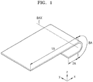
- FIG. 1 is a schematic perspective view of a display apparatus according to an embodiment
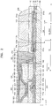
- FIG. 2 is a schematic cross-sectional view of a part of the display apparatus of FIG. 1
- FIG. 3 is a schematic plan view of a part of the display apparatus of FIG. 1 .
- a substrate 100 in the display apparatus includes a bending area BA extending in a first direction (+y direction).
- the bending area BA is between a first area 1A and a second area 2A in a second direction (+x direction) crossing the first direction.
- the substrate 100 is bent about a bending axis BAX extending in the first direction (+y direction) as shown in FIG. 1 .
- the substrate 100 may include various materials having flexible or bendable characteristics, e.g., polymer resins such as polyethersulphone (PES), polyacrylate, polyetherimide (PEI), polyethylene naphthalate (PEN), polyethylene terephthalate (PET), polyphenylene sulfide (PPS), polyarylate (PAR), polyimide (PI), polycarbonate (PC), and cellulose acetate propionate (CAP).
- the substrate 100 may have a multi-layered structure including two layers having one or more of the above polymer resins, as well as a barrier layer including an inorganic material such as silicon oxide, silicon nitride, and silicon oxynitride between the two layers.
- the substrate 100 has a constant width in a y-axis direction throughout the first area 1A, the bending area BA, and the second area 2A, but is not limited thereto.
- the substrate 100 may have a width varying in the y-axis direction within the first area 1A.
- a narrower width of the substrate 100 within the first area 1A may be equal to the width of the substrate within the bending area BA or in the second area 2A, as shown in FIG. 3 .
- the first area 1A includes a display area DA.
- the first area 1A may further include a part of a non-display area outside the display area DA, in addition to the display area DA, as shown in FIG. 2 .
- the second area 2A may also include the non-display area.
- a thin film transistor (TFT) 210 electrically connected to a display device 300 may be located in addition to the display device 300, as shown in FIG. 2 .
- an organic light-emitting device is located in the display area DA as the display device 300. Electric connection of the organic light-emitting device to the TFT 210 may be understood as a pixel electrode 310 being electrically connected to the TFT 210.
- the TFT 210 may include a semiconductor layer 211 including amorphous silicon, polycrystalline silicon, or an organic semiconductor material.
- the TFT 210 may also include a gate electrode 213, a source electrode 215a, and a drain electrode 215b.
- a gate insulating layer 120 may be formed between the semiconductor layer 211 and the gate electrode 213, wherein the gate insulating layer 120 includes an inorganic material such as silicon oxide, silicon nitride, and/or silicon oxynitride.
- an interlayer insulating layer 130 may be on the gate electrode 213, and the source electrode 215a and the drain electrode 215b may be on the interlayer insulating layer 130, wherein the interlayer insulating layer 130 includes an inorganic material such as silicon oxide, silicon nitride, and/or silicon oxynitride.
- the insulating layers including the inorganic material may be formed by chemical vapor deposition (CVD) or atomic layer deposition (ALD). This will be applied to other embodiments and modifications thereof that will be described later.
- a buffer layer 110 may be between the TFT 210 having the above structure and the substrate 100.
- the buffer layer 110 may include an inorganic material such as silicon oxide, silicon nitride, and/or silicon oxynitride.
- the buffer layer 110 may improve smoothness of the upper surface of the substrate 100, or prevent or reduce infiltration of impurities from the substrate 100 into the semiconductor layer 211 of the TFT 210.
- a planarization layer 140 may be arranged on the TFT 210.
- the planarization layer 140 may planarize an upper portion of the TFT 210.
- the planarization layer 140 may include, for example, an organic material such as acryl, benzocyclobutene (BCB), and hexamethyldisiloxane (HMDSO).
- the planarization layer 140 may be variously modified.
- the planarization layer 140 may have a multi-layered structure.
- FIG. 2 shows that the planarization layer 140 may have a multi-layered structure.
- the planarization layer 140 may have an opening outside the display area DA, so that a part of the planarization layer 140 in the display area DA and a part of the planarization layer 140 in the second area 2A may be physically separate from each other. Thus, impurities from outside may not reach the display area DA via the planarization layer 140.
- the display device 300 may be on the planarization layer 140.
- the display device 300 may be an organic light-emitting device including the pixel electrode 310, an opposite electrode 330, and an intermediate layer 320 between the pixel electrode 310 and the opposite electrode 330 and including an emission layer.
- the pixel electrode 310 may contact one of the source electrode 215a and the drain electrode 215b via an opening formed in the planarization layer 140 and may be electrically connected to the TFT 210, as shown in FIG. 2 .
- a pixel defining layer 150 may be on the planarization layer 140.
- the pixel defining layer 150 includes openings corresponding respectively to sub-pixels, that is, at least an opening exposing a center portion of the pixel electrode 310, to define pixels. Also, in the example shown in FIG. 2 , the pixel defining layer 150 increases a distance between an edge of the pixel electrode 310 and the opposite electrode 330 above the pixel electrode 310 so as to prevent an arc from being generated at the edge of the pixel electrode 310.
- the pixel defining layer 150 may include an organic material, for example, PI or HMDSO.
- the intermediate layer 320 of the organic light-emitting device may include low-molecular weight organic materials or polymer materials.
- the intermediate layer 320 may include a hole injection layer (HIL), a hole transport layer (HTL), an emission layer (EML), an electron transport layer (ETL), and an electron injection layer (EIL) in a single or multiple-layered structure
- examples of organic materials may include copper phthalocyanine (CuPc), N,N'-Di(naphthalene-1-yl)-N,N'-diphenyl-benzidine (NPB), and tris-8-hydroxyquinoline aluminum (Alq 3 ).
- the low-molecular weight organic materials may be deposited by a vacuum deposition method.
- the intermediate layer 320 may include an HTL and an EML.
- the HTL may include poly(3,4-ethylenedioxythiophene (PEDOT)
- the EML may include a poly-phenylenevinylene (PPV)-based or polyfluorene-based polymer material.
- the intermediate layer 320 above may be formed by a screen printing method, an inkjet printing method, or a laser induced thermal imaging (LITI) method.
- the intermediate layer 320 is not limited to the above example, and may have various structures.
- the intermediate layer 320 may include a layer that is integrally formed across a plurality of pixel electrodes 310, or a layer that is patterned to correspond to each of the plurality of pixel electrodes 310.
- the opposite electrode 330 is arranged above the display area DA, and as shown in FIG. 2 , may cover the display area DA. That is, the opposite electrode 330 may be integrally formed with respect to a plurality of organic light-emitting devices, so as to correspond to a plurality of pixel electrodes 310.
- an encapsulation layer 400 may cover the organic light-emitting device to protect the organic light-emitting device.
- the encapsulation layer 400 covers the display area DA, and may also extend outside the display area DA.
- the encapsulation layer 400 may include a first inorganic encapsulation layer 410, an organic encapsulation layer 420, and a second inorganic encapsulation layer 430, as shown in FIG. 2 .
- the first inorganic encapsulation layer 410 covers the opposite electrode 330, and may include silicon oxide, silicon nitride, and/or silicon oxynitride. If desired, other layers such as a capping layer may be arranged between the first inorganic encapsulation layer 410 and the opposite electrode 330. Since the first inorganic encapsulation layer 410 is shaped according to its underlying structures, the first inorganic encapsulation layer 410 may have an uneven upper surface.
- the organic encapsulation layer 420 covers the first inorganic encapsulation layer 410, and unlike the first inorganic encapsulation layer 410, the organic encapsulation layer 420 may have an even or substantially flat upper surface.
- the organic encapsulation layer 420 may substantially have an even upper surface at a portion corresponding to the display area DA.
- the organic encapsulation layer 420 may include at least one material selected from PET, PEN, PC, PI, polyethylene sulfonate, polyoxymethylene, polyarylate, and hexamethyldisiloxane.
- the second inorganic encapsulation layer 430 covers the organic encapsulation layer 420, and may include silicon oxide, silicon nitride, and/or silicon oxynitride. The second inorganic encapsulation layer 430 may contact the first inorganic encapsulation layer 410 at an edge thereof outside the display area DA, in order not to expose the organic encapsulation layer 420 to the outside.
- the encapsulation layer 400 includes the first inorganic encapsulation layer 410, the organic encapsulation layer 420, and the second inorganic encapsulation layer 430, even if there is a crack in the encapsulation layer 400 in the above multi-layered structure, the crack may be disconnected between the first inorganic encapsulation layer 410 and the organic encapsulation layer 420 or between the organic encapsulation layer 420 and the second inorganic encapsulation layer 430. As such, the likelihood of forming a path through which external moisture or oxygen may infiltrate into the display area DA may be reduced.
- a polarization plate 520 may be attached on the encapsulation layer 400 via an optically clear adhesive (OCA) 510.
- OCA optically clear adhesive
- the polarization plate 520 may reduce reflection of external light. For example, when external light that passes through the polarization plate 520 is reflected by an upper surface of the opposite electrode 330 and then passes through the polarization plate 520 again, the external light passes through the polarization plate 520 twice and a phase of the external light may be changed. Therefore, a phase of reflected light is different from the phase of the external light entering the polarization plate 520 and thus destructive interference occurs. Accordingly, reflection of external light may be reduced and visibility may be improved.
- the OCA 510 and the polarization plate 520 may cover an opening in the planarization layer 140, as shown in FIG.
- the display apparatus may not necessarily include the polarization plate 520, and if desired, the polarization plate 520 may be omitted or replaced by other elements.
- the polarization plate 520 may be omitted, and a black matrix and a color filter may be used to reduce reflection of external light.
- the buffer layer 110, the gate insulating layer 120, and the interlayer insulating layer 130 including the inorganic material may be collectively referred to as an inorganic insulating layer.
- the inorganic insulating layer may include a first feature that is a first opening corresponding to the bending area BA, as shown in FIG. 2 . That is, the buffer layer 110, the gate insulating layer 120, and the interlayer insulating layer 130 may respectively include openings 110a, 120a, and 130a corresponding to the bending area BA. That the first opening corresponds to the bending area BA may denote that the opening overlaps the bending area BA. Here, an area of the first opening may be greater than that of the bending area BA. To do this, in FIG.
- a width OW of the first opening is greater than a width BAw of the bending area BA.
- the area of the first opening may be defined as the smallest area among areas of the openings 110a, 120a, and 130a, of the buffer layer 110, the gate insulating layer 120, and the interlayer insulating layer 130.
- the area of the first opening is defined by an area of the opening 110a in the buffer layer 110.
- the opening 120a of the gate insulating layer 120 and the opening 130a of the interlayer insulating layer 130 may be simultaneously formed.
- the TFT 210 in order for the source electrode 215a and the drain electrode 215b to contact the semiconductor layer 211, contact holes penetrating through the gate insulating layer 120 and the interlayer insulating layer 130 have to be formed.
- the opening 120a of the gate insulating layer 120 and the opening 130a of the interlayer insulating layer 130 may be simultaneously formed when forming the contact holes. Accordingly, an internal surface of the opening 120a of the gate insulating layer 120 and an internal surface of the opening 130a of the interlayer insulating layer 130 may form a single continuous surface as shown in FIG. 2 .
- the display apparatus includes an organic material layer 160 at least partially filling the first opening of the inorganic insulating layer. In FIG. 2 , the organic material layer 160 completely fills the first opening.
- the display apparatus according to the embodiment includes a first conductive layer 215c, and the first conductive layer 215c extends from the first area 1A to the second area 2A across the bending area BA and above the organic material layer 160.
- the first conductive layer 215c may also extend over an inorganic insulating layer such as the interlayer insulating layer 130, where the organic material layer 160 is not provided.
- the first conductive layer 215c may be formed simultaneously with the source electrode 215a or the drain electrode 215b by using the same material as that of the source electrode 215a or the drain electrode 215b.
- FIG. 2 shows a state in which the display apparatus is not bent for convenience of description
- the display apparatus according to the embodiment is actually in a state in which the substrate 100 is bent at the bending area BA, as shown in FIG. 1 .
- the display apparatus is manufactured so that the substrate 100 is flat, as shown in FIG. 2 , and after that, the substrate 100 is bent at the bending area BA so that the display apparatus may have the shape as shown in FIG. 1 .
- tensile stress may be induced in the first conductive layer 215c.
- the occurrence of defects in the first conductive layer 215c during the bending process may be prevented or reduced.
- the inorganic insulating layers such as the buffer layer 110, the gate insulating layer 120, and/or the interlayer insulating layer 130 do not include openings corresponding to the bending area BA, but continuously extend from the first area 1A to the second area 2A, and if the first conductive layer 215c is on such an inorganic insulating layer, large tensile stress is applied to the first conductive layer 215c during bending of the substrate 100.
- the inorganic insulating layer has a greater hardness than that of the organic material layer, cracks are likely to form in the inorganic insulating layer in the bending area BA, and when a crack occurs in the inorganic insulating layer, a crack may also occur in the first conductive layer 215c on the inorganic insulating layer and thus the probability of generating defects such as disconnections in the first conductive layer 215c increases greatly.
- the inorganic insulating layer includes the first opening corresponding to the bending area BA, and the part of the first conductive layer 215c which corresponds to the bending area BA is on the organic material layer 160 that at least partially fills the first opening. Since the inorganic insulating layer includes the first opening corresponding to the bending area BA, the possibility of cracks occurring in the inorganic insulating layer is greatly decreased, and the organic material layer 160 is less likely to have cracks due to characteristics of the organic material. Therefore, the occurrence of cracks in the portion of the first conductive layer 215c on the organic material layer 160 may be prevented or reduced, wherein the portion of the first conductive layer 215c corresponds to the bending area BA.
- the organic material layer 160 may absorb the tensile stress generated due to the bending of the substrate 100 so as to reduce concentration of the tensile stress in the first conductive layer 215c.
- the inorganic insulating layer has the first opening, but is not limited thereto.
- the inorganic insulating layer may have a first feature that is a first recess, rather than the first opening.
- the buffer layer 110 may not include the opening 110a unlike the example shown in FIG. 2 , but may extend in continuous manner from the first area 1A to the second area 2A across the bending area BA. Then, the gate insulating layer 120 and the interlayer insulating layer 130 may only include the openings 120a and 130a.
- the buffer layer 110, the gate insulating layer 120, and the interlayer insulating layer 130, which include the inorganic material may be collectively referred to as an inorganic insulating layer, and in this case, the inorganic insulating layer may be understood to have the first recess corresponding to the bending area BA.
- the organic material layer 160 may at least partially fill the first recess.
- the inorganic insulating layer since the inorganic insulating layer has the first recess corresponding to the bending area BA, a thickness of the inorganic insulating layer is reduced in the bending area BA, and accordingly, the substrate 100 may be more easily bent.
- the organic material layer 160 is in the bending area BA and the first conductive layer 215c is above the organic material layer 160, damage to the first conductive layer 215c during the bending operation may be effectively prevented.
- An example in which the inorganic insulating layer includes the first opening is described in the above embodiments and other embodiments that will be described later, or modified examples thereof for convenience of description, but the inorganic insulating layer may instead include the first recess as described above.
- the display apparatus may include second conductive layers 213a and 213b, in addition to the first conductive layer 215c.
- the second conductive layers 213a and 213b are located above the first area 1A or the second area 2A to be located at a different layer from that of the first conductive layer 215c, and may be electrically connected to the first conductive layer 215c.
- the second conductive layers 213a and 213b are at the same layer, that is, on the gate insulating layer 120, and use the same material as that of the gate electrode 213.
- the first conductive layer 215c contacts the second conductive layers 213a and 213b via contact holes in the interlayer insulating layer 130.
- the second conductive layer 213a is in the first area 1A
- the second conductive layer 213b is in the second area 2A.
- the second conductive layer 213a in the first area 1A may be electrically connected to the TFT 210 in the display area DA, and accordingly, the first conductive layer 215c may be electrically connected to the TFT 210 in the display area DA via the second conductive layer 213a.
- the second conductive layer 213b in the second area 2A may also be electrically connected to the TFT 210 of the display area DA, via the first conductive layer 215c.
- the second conductive layers 213a and 213b that are outside the display area DA may be electrically connected to the elements in the display area DA, or may extend toward the display area DA so that at least some parts of the second conductive layers 213a and 213b may be located in the display area DA.
- FIG. 2 shows a state in which the display apparatus is not bent for convenience of description
- the display apparatus according to the embodiment is actually in a state in which the substrate 100 is bent at the bending area BA, as shown in FIG. 1 .
- the display apparatus is manufactured so that the substrate 100 is flat, as shown in FIG. 2 , and after that, the substrate 100 is bent at the bending area BA so that the display apparatus may have the shape as shown in FIG. 1 .
- tensile stress may be applied to the elements in the bending area BA.
- the first conductive layer 215c crossing over the bending area BA includes a material having high elongation rate, so that defects such as cracks in the first conductive layer 215c or disconnection of the first conductive layer 215c may be prevented.
- the second conductive layers 213a and 213b including a material having an elongation rate lower than that of the first conductive layer 215c and electrical/physical characteristics different from those of the first conductive layer 215c, are formed in the first area 1A or the second area 2A, and thus, an efficiency of transferring electric signals in the display apparatus may be improved or a defect rate during the manufacturing processes of the display apparatus may be reduced.
- the second conductive layers 213a and 213b may include molybdenum
- the first conductive layer 215c may include aluminum.
- the first conductive layer 215c and the second conductive layers 213a and 213b may have multi-layered structures, if desired.
- the first conductive layer 215c may have a multi-layered structure such as a titanium layer/aluminum layer/titanium layer structure
- the second conductive layers 213a and 213b may each have a multi-layered structure such as a molybdenum layer/titanium layer structure.
- the first conductive layer 215c may extend to the display area to be electrically connected directly to the source electrode 215a, the drain electrode 215b, or the gate electrode 213 of the TFT 210.
- the organic material layer 160 may cover an internal surface of the first opening of the inorganic insulating layer.
- the first conductive layer 215c may include the same material as, and may be formed simultaneously with, the source electrode 215a and the drain electrode 215b, a conductive layer may be formed on the interlayer insulating layer 130 over an entire surface of the substrate 100 and may be patterned to form the source electrode 215a, the drain electrode 215b, and the first conductive layer 215c.
- the organic material layer 160 does not cover the inner side surfaces of the opening 110a in the buffer layer 110, the opening 120a in the gate insulating layer 120, or the opening 130a in the interlayer insulating layer 130, the conductive material of the conductive layer may not be removed from, but may remain on, these inner side surfaces. In this case, the remaining conductive material may cause shorts between different conductive layers.
- the organic material layer 160 may cover the inner side surface of the first opening in the inorganic insulating layer. If the organic material layer 160 includes a second feature that is a second opening 160a that will be described later, in order to make the organic material layer 160 cover the internal surface of the first opening in the inorganic insulating layer, a width OW of the inorganic insulating layer in a direction from the first area 1A towards the second area 2A may be greater than a length d of the second opening 160a of the organic material layer 160 in a direction in which the second opening 160a extends.
- the organic material layer 160 is shown to have a largely constant thickness, but the organic material layer 160 may have a thickness that varies depending on locations therein, so that an upper surface of the organic material layer 160 may have a gradual curve near edges of the opening 110a in the buffer layer 110, the opening 120a in the gate insulating layer 120, and the opening 130a in the interlayer insulating layer 130. Accordingly, remaining conductive material that should have been removed may be prevented during patterning the conductive layer in order to form the source electrode 215a, the drain electrode 215b, and the first conductive layer 215c.
- a bending protection layer (BPL) 600 may be located outside the display area DA. That is, the BPL 600 may be located above the first conductive layer 215c, corresponding at least to the bending area BA.
- the stress neutral plane may be adjusted to be around the first conductive layer 215c via the BPL 600, and thus, the tensile stress applied to the first conductive layer 215c may be reduced or a compressive stress may be applied to the first conductive layer 215c.
- the BPL 600 may include acryl. When compressive stress is applied to the first conductive layer 215c, the possibility of damaging the first conductive layer 215c is much less than when tensile stress is applied to the first conductive layer 215c.
- an end surface of the BPL 600 facing an edge of the substrate 100 (+y direction) does not coincide with an end surface of the substrate 100, but is located on a top surface of the substrate 100.
- the end surface of the BPL 600 may correspond to the end surface of the substrate 100 (see FIG. 15 ).
- an additional BPL that is spaced apart from the BPL 600 to be located closer to the edge of the substrate 100 (+y direction) may be provided. This may be understood that the BPL 600 has an opening that penetrates through the BPL in an up-and-down direction, similarly to the second opening 160a of the organic material layer 160 which will be described later.
- the BPL 600 may be formed before the cutting process.
- the BPL is also cut when the mother substrate is cut, and accordingly, the end surface of the BPL 600 may correspond to the end surface of the substrate 100.
- the cutting may be performed by irradiating a laser beam to the mother substrate.
- an upper surface of the BPL 600 in a direction towards the display area DA (-x direction) corresponds to an upper surface of the polarization plate 520 (in the +z direction), but is not limited thereto.
- an end of the BPL 600 in the direction towards the display area DA (-x direction) may partially cover an upper surface at the edge of the polarization plate 520. Otherwise, the end of the BPL 600 in the direction towards the display area DA (-x direction) may not contact the polarization plate 520 and/or the OCA 510. In the latter case, during or after forming the BPL 600, movement of gas generated from the BPL 600 in a direction toward the display area DA (-x direction), which risks degrading the display device 300, may be prevented.
- a thickness of the BPL 600 corresponding to the display area DA (-x direction) may be greater than that of the other portions in the BPL 600.
- a volume of the BPL 600 may be reduced through the hardening process.
- the portion of the BPL 600 corresponding to the display area DA (-x direction) is in contact with the polarization plate 520 and/or the OCA 510, the portion of the BPL 600 is fixed at the location, and thus, a volume reduction occurs in the remaining portion of the BPL 600. Therefore, the thickness of the BPL 600 corresponding or proximate to the display area DA (-x direction) may be greater than that of the rest of the BPL 600.
- the organic material layer 160 in the display apparatus includes the second opening 160a extending along an edge of the substrate 100 as shown in FIG. 3 .
- the organic material layer 160 includes second openings 160a that extend proximate to the edges of the substrate 100. Since the organic material layer 160 has the second openings 160a, occurrence of defects during manufacturing the display apparatus or using the display apparatus that is manufactured may be reduced.
- FIG. 3 shows a state in which the substrate 100 is not bent for convenience of description
- the display apparatus according to the embodiment is actually bent at the bending area BA, as shown in FIG. 1 . Therefore, the bending area BA is located at an edge of the display apparatus.
- shock may be applied to the bending area BA.
- shock is more likely to be applied to an edge of the bending area BA in the +y direction or -y direction, and in this case, as shown in FIG. 4 that is a schematic cross-sectional view taken along a line IV-IV of FIG. 3 , crack CR may occur in the organic material layer 160 due to external shock. If such a crack CR reaches a center portion of the bending area BA, cracks may also occur in wires such as the first conductive layer 215c, generating defects in the display apparatus.
- the organic material layer 160 includes the second openings 160a as described above.
- the second openings 160a extend along the edges of the substrate 100 (in the +x direction when viewed as if the substrate 100 is not bent). Therefore, even if the crack CR occurs at the edge of the organic material layer 160 as shown in FIG. 4 , the crack CR may not reach the center portion of the bending area BA, but may be stopped by the second openings 160a. As such, even if shock is applied to an outer portion of the bending area BA during manufacturing processes or afterward, generation of defects due to cracks in the display apparatus may be prevented or reduced.
- a length d of the second opening 160a in its lengthwise direction may be greater than the width BAw of the bending area BA from the first area 1A to the second area 2A. As such, occurrence of cracks in the entire bending area BA due to shock applied to the edge of the substrate 100 may be prevented or reduced.
- the second openings 160a of the organic material layer 160 may not necessarily penetrate through the organic material layer 160 as above.
- the organic material layer 160 may include a second feature that is a second recess 160a, rather than the second opening.
- propagation of cracks CR generated in the organic material layer 160 towards the center portion of the bending area BA may be effectively prevented by the second recess 160a.
- the above and other descriptions of the second opening may be applied to the second recess 160a.
- the planarization layer 140 above the organic material layer 160 may also include a third feature that is a third opening 140a corresponding to the second opening 160a.
- the third opening 140a of the planarization layer 140 may extend along an edge of the substrate 100 like the second opening 160a of the organic material layer 160. That is, similar to the second opening 160a shown in FIG. 3 , the planarization layer 140 may have third openings 140a extending along the edges of the substrate 100.
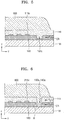
- the third openings 140a extend along the edge of the substrate 100 (in the +x direction when viewed as if the substrate 100 is not bent). Therefore, as shown in FIG. 6 , even if crack CR occurs at the edge of the organic material layer 160 and/or the planarization layer 140, the crack CR may not reach the center portion of the bending area BA, but may be stopped around the second opening 160a and the third opening 140a. As such, even if shock is applied to the outer portion of the bending area BA during manufacturing processes or utilizing processes after manufacturing, defects caused by cracks in the display apparatus may be prevented or reduced.
- a length of the third opening 140a of the planarization layer 140 may be greater than the width BAw of the bending area BA from the first area 1A to the second area 2A. As such, occurrence of cracks in the entire bending area BA due to shock applied to the edge of the substrate 100 may be prevented or reduced.
- the planarization layer 140 may not necessarily have the third opening 140a penetrating through the planarization layer 140 as above. That is, the planarization layer 140 may include a third feature that is a third recess, not the third opening 140a. This is also applied to the above-described embodiments, embodiments that will be described later, or modified examples thereof.
- the embodiment may be variously modified, for example, the organic material layer 160 may not include the second opening 160a or the second recess 160a and the planarization layer 140 may only include the third opening 140a or the third recess. This is also applied to the above-described embodiments, embodiments that will be described later, or modified examples thereof.
- the BPL 600 may at least partially fill the second opening 160a or at least partially fill the third opening 140a.
- the BPL 600 may not only fill the second opening 160a or the third opening 140a at least partially, but may also cover the bending area BA.
- the BPL 600 adjusts the location of a stress neutral plane. If the BPL 600 does not fill the second opening 160a or the third opening 140a, the stress neutral plane is located at an intermediate portion between the upper and lower surfaces of the substrate 100 under the second opening 160a or the third opening 140a, and peripheral portions thereof. Accordingly, when the substrate 100 is bent, compressive stress is applied to a part, e.g., from a center portion toward the lower surface, of the substrate 100, but tensile stress is applied to a part, e.g., from the center portion toward the upper surface, of the substrate 100. Accordingly, cracks or tears may occur between the center portion and the upper surface of the substrate 100.
- the BPL 600 fills at least partially the second opening 160a or the third opening 140a so as to adjust the location of the stress neutral plane, and thus, occurrence of defects in the substrate 100 may be prevented or reduced. Even if a crack CR occurs in the organic material layer 160 and/or the planarization layer 140, the second opening 160a or the third opening 140a may prevent or reduce propagation of the crack CR toward the center portion of the bending area BA.
- the planarization layer 140 may cover an internal side surface of the second opening 160a in the organic material layer 160.
- the first conductive layer 215c may be simultaneously formed with the source electrode 215a and the drain electrode 215b by using the same material as that of the source and drain electrodes 215a and 215b.
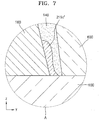
- a conductive layer is formed above the organic material layer 160 and/or the interlayer insulating layer 130 throughout almost the entire surface of the substrate 100, and is then patterned to form the source electrode 215a, the drain electrode 215b, and the first conductive layer 215c. Therefore, as shown in FIG. 7 that is an enlarged cross-sectional view of a part A of FIG. 6 , a conductive material may remain on the internal side surface of the second opening 160a in the organic material layer 160, and thus, a conductive remaining layer 215c' may remain at least partially along the internal side surface of the second opening 160a.
- the conductive remaining layer 215c' may cause shorts between two different conductive layers, or cause defects.
- a material for forming the pixel electrode 310 may agglomerate around the conductive remaining layer 215c'. This is because, if the conductive remaining layer 215c' includes aluminum and the pixel electrode 310 includes silver (Ag), this silver may react with aluminum to form a lump around the conductive remaining layer 215c'.
- the planarization layer 140 covers the internal side surface of the second opening 160a in the organic material layer 160 so as to cover the conductive remaining layer 215c', the conductive remaining layer 215c' may not be exposed. As such, occurrence of defects during manufacturing processes may be prevented or reduced. Since the conductive remaining layer 215c' may be generated when the first conductive layer 215c is formed as described above, the conductive remaining layer 215c' may include at least some of the materials included in the first conductive layer 215c. As described above, the first conductive layer 215c may include titanium or aluminum, and if desired, may have a multi-layered structure including titanium layer/aluminum layer/titanium layer. Therefore, the conductive remaining layer 215c' may also include titanium, aluminum, or a mixture or a compound thereof.
- FIG. 8 is a schematic cross-sectional view taken along a line VIII-VIII of FIG. 3 .
- the length d (see FIG. 3 ) of the second opening 160a in the organic material layer 160 may be greater than the length of the third opening 140a in the planarization layer 140.
- the planarization layer 140 may cover the conductive material that may remain on the internal side surface of the second opening 160a.
- the organic material layer 160 may include an additional opening 160b or an additional recess.
- the additional opening 160b or the additional recess may extend along the edge of the substrate 100 adjacent to the second opening 160a.
- propagation of the crack CR (see FIGS. 4 to 6 ) towards the center portion of the bending area BA may be blocked twice.
- FIG. 9 shows a state in which the substrate 100 is not bent for convenience of description
- the display apparatus according to the embodiment is actually bent at the bending area BA, as shown in FIG. 1 . Therefore, unlike that shown in FIG. 9 , the bending area BA is located at the edge of the display apparatus, and in particular, a virtual line IL that is in parallel with the bending axis BAX (see FIG. 1 ) and crosses a center of the bending area BA, is located at the edge of the display apparatus. Therefore, external shock may be applied to the portion of the bending area BA on which the virtual line IL is located.
- the additional opening 160b or the additional recess of the organic material layer 160 is located to cross the virtual line IL, so as to doubly prevent crack CR from proceeding towards the center portion of the bending area BA. That is, although a length of the additional opening 160b or the additional recess may be less than that of the second opening 160a, the additional opening 160b or the additional recess may still cross the virtual line IL.
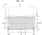
- the second opening 160a in the organic material layer 160 may have a variable width. That is, the second opening 160a may have a greater width at a portion crossing the virtual line IL that is parallel with the bending axis BAX (see FIG. 1 ) and crossing the center of the bending area BA, than that of at least one other portion. The greater the width of the second opening 160a is, the less the possibility of propagating the crack CR at that location. Also, as shown in FIG.
- the second opening 160a extends along the edge of the substrate 100, but an intermediate portion of the second opening 160a in a length direction thereof is curved towards the center of the bending area BA so that the second opening 160a may have a meniscus shape.
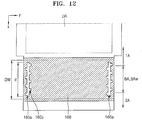
- the organic material layer 160 may further include an auxiliary opening 160c or an auxiliary recess.
- the auxiliary opening 160c or the auxiliary recess may be connected to the second opening 160a and may extend in a direction crossing the lengthwise direction of the second opening 160a.
- the organic material layer 160 may have a plurality of auxiliary openings 160c or a plurality of auxiliary recesss, and in this case, the auxiliary openings 160c or the auxiliary recesss may be located alternately at opposite sides of the second opening 160a in the direction in which the second opening 160a extends.
- the second opening 160a of the organic material layer 160 extends along the edge of the substrate 100, and a plurality of islands of the organic material layer 160 may be located therein.
- the second opening or the second recess extends along the edge of the substrate 100, but one or more embodiments are not limited thereto.
- the second opening or the second recess may not be formed in the organic material layer 160, but may be formed in another portion.
- the insulating layer disposed between the substrate 100 and the first conductive layer 215c may have a first opening or a first recess that extends in a direction crossing the bending axis BAX to correspond to a portion between the edge of the substrate 100 and the first conductive layer 215c at the bending area BA.
- the portion between the edge of the substrate 100 and the first conductive layer 215c may be understood as a portion between the edge of the substrate 100 and a first conductive layer among the plurality of first conductive layers 215c which is closest to the edge of the substrate 100.
- FIG. 14 is a schematic plan view of a part of a display apparatus according to an embodiment
- FIG. 15 is a schematic cross-sectional view taken along a line XV-XV of FIG. 14
- the display apparatus according to the embodiment is different from the display apparatus according to the previous embodiment illustrated with reference to FIG. 3 in view of a shape of a second opening 160a' in the organic material layer 160.
- the second opening 160a' of the organic material layer 160 may extend to the end of the substrate 100 (in the +y direction or -y direction).
- the planarization layer 140 may extend to the edge of the substrate 100 so as to fill the extended second opening 160a' of the organic material layer 160.
- a side end surface of the planarization layer 140 and a side end surface of the BPL 600 roughly correspond to a side end surface of the substrate 100, and thus, the edge of the substrate 100 may be sufficiently supported by the planarization layer 140 and/or the BPL 600 even when the organic material layer 160 includes the second opening 160a'.
- the substrate 100 that is flexible or bendable is very small in thickness, unintentional deformation of the substrate 100 may be effectively prevented.
- a third opening 140a' of the planarization layer 140 may extend to the end of the substrate 100 (in the +y direction or -y direction).
- the side end surface of the BPL 600 roughly corresponds to the side end surface of the substrate 100, and thus, the BPL 600 may sufficiently support the edge of the substrate 100 even when the organic material layer 160 includes the extended second opening 160a' and the planarization layer 140 includes the extended third opening 140a'.
- the substrate 100 that is flexible or bendable is very small in thickness, unintentional deformation of the substrate 100 may be effectively prevented.
- the organic material layer 160 may extend to the edge of the substrate 100 and the planarization layer 140 has a third opening 140a' that may extend to the end of the substrate 100 (in the +y direction or -y direction).
- the side end surface of the BPL 600 may roughly correspond to the side end surface of the substrate 100.
- the organic material layer 160 includes the second opening 160a' extending to the edge of the substrate 100 or the planarization layer 140 includes the third opening 140a' extending to the edge of the substrate 100, but one or more embodiments are not limited thereto.
- the organic material layer 160 may include a second recess extending to the edge of the substrate 100
- the planarization layer 140 may include a third recess extending to the edge of the substrate 100.
- the display apparatus capable of reducing generation of defects during or after manufacturing may be implemented.
- the scope of the inventive concept is not limited to the above effects.
Landscapes
- Engineering & Computer Science (AREA)
- Physics & Mathematics (AREA)
- Microelectronics & Electronic Packaging (AREA)
- Optics & Photonics (AREA)
- Chemical & Material Sciences (AREA)
- Inorganic Chemistry (AREA)
- Manufacturing & Machinery (AREA)
- General Physics & Mathematics (AREA)
- Theoretical Computer Science (AREA)
- Electroluminescent Light Sources (AREA)
- Devices For Indicating Variable Information By Combining Individual Elements (AREA)
Abstract
Description
- One or more embodiments of the invention relate to a display apparatus, and more particularly, to a display apparatus capable of reducing occurrence of defects during manufacture or in subsequent use.
- In general, a display apparatus includes a display unit above a substrate. When such a display apparatus is at least partially bent, visibility at various angles may be improved or the size of a non-display area may be reduced.
- However, in a display apparatus according to the prior art, defects may occur at a bending portion or nearby, during manufacture or later use.
- One or more embodiments of the invention seek to provide a display apparatus capable of reducing occurrence of defects during manufacturing of the display apparatus or while in use after being manufactured.
- Additional aspects will be set forth in part in the description which follows and, in part, will be apparent from the description, or may be learned by practice of the presented or other embodiments.
- According to one or more embodiments, a display apparatus includes: a substrate including a bending area between a first area and a second area, the substrate being bent in the bending area about a bending axis; an inorganic insulating layer over the substrate and including a first feature that is a first opening or a first recess, the first feature positioned to correspond to the bending area; and an organic material layer at least partially filling the first feature, and including a second feature that is a second opening or a second recess, the second feature extending along an edge of the substrate.
- At least one of the first opening and the first recess may overlap the bending area. An area of the first opening or the first recess may be greater than an area of the bending area. A length of the second opening or the second recess may be greater than a width of the bending area in a direction from the first area to the second area.
- The display apparatus may further include a first conductive layer over the organic material layer, the first conductive layer extending from the first area to the second area across the bending area.
- A width of one of the first opening and the first recess may be greater than a length of one of the second opening and the second recess. The display apparatus may further include an additional organic material layer covering the first conductive layer and the organic material layer, wherein the additional organic material layer may include a third feature that is a third opening or a third recess, the third feature extending along the edge of the substrate so as to correspond to the second opening or the second recess.
- A length of one of the second opening and the second recess may be greater than a length of one of the third opening and the third recess.
- The additional organic material layer may cover a side of the second opening or the second recess. The display apparatus may further include a conductive remaining layer over at least a part of a side of the second opening or the second recess, wherein the additional organic material layer may cover the conductive remaining layer. The conductive remaining layer may include a same material as the first conductive layer.
- The display apparatus may further include a second conductive layer in the first area or the second area so as to be located on a layer different from a layer on which the first conductive layer is located, the second conductive layer being electrically connected to the first conductive layer. An elongation rate of the first conductive layer may be greater than an elongation rate of the second conductive layer.
- The organic material layer may include an additional opening or an additional recess extending along an edge of the substrate to be adjacent to the second opening or the second recess. A length of the additional opening or the additional recess may be less than a length of the second opening or the second recess, and the additional opening or the additional recess may cross a virtual line extending parallel with the bending axis and crossing a center of the bending area.
- The second opening or the second recess may have a first width at a first portion proximate to a center of the bending area and a second width remote from the first portion, the first width being greater than the second width.
- The organic material layer may further include an auxiliary opening or an auxiliary recess connected to the second opening or the second recess and extending in a direction crossing a direction in which the second opening or the second recess extends.
- The display apparatus may further include a bending protection layer filling the second opening or the second recess. The bending protection layer may cover the bending area.
- At least some of the above features and other features according to the invention are set out in the claims.
- According to one or more embodiments, a display apparatus includes: a substrate including a bending area between a first area and a second area, the substrate being bent in the bending area about a bending axis; a first conductive layer extending from the first area to the second area across the bending area; and an insulating layer between the substrate and the first conductive layer and including an opening or a recess, the opening or recess extending in a direction crossing the bending axis so as to correspond to a portion between an edge of the substrate and the first conductive layer in the bending area.
- The above and/or other aspects of the invention will become apparent and more readily appreciated from the following description of the embodiments, taken in conjunction with the accompanying drawings in which:
-
FIG. 1 is a schematic perspective view of a part of a display apparatus according to an embodiment; -
FIG. 2 is a schematic cross-sectional view of a part of the display apparatus ofFIG. 1 ; -
FIG. 3 is a schematic plan view of a part of the display apparatus ofFIG. 1 ; -
FIG. 4 is a schematic cross-sectional view taken along a line IV-IV ofFIG. 3 ; -
FIG. 5 is a schematic cross-sectional view of a part of a display apparatus according to an embodiment; -
FIG. 6 is a schematic cross-sectional view of a part of a display apparatus according to an embodiment; -
FIG. 7 is an enlarged cross-sectional view of a part A ofFIG. 6 ; -
FIG. 8 is a schematic cross-sectional view taken along a line VIII-VIII ofFIG. 3 ; -
FIG. 9 is a schematic plan view of a part of a display apparatus according to an embodiment; -
FIG. 10 is a schematic plan view of a part of a display apparatus according to an embodiment; -
FIG. 11 is a schematic plan view of a part of a display apparatus according to an embodiment; -
FIG. 12 is a schematic plan view of a part of a display apparatus according to an embodiment; -
FIG. 13 is a schematic plan view of a part of a display apparatus according to an embodiment; -
FIG. 14 is a schematic plan view of a part of a display apparatus according to an embodiment; -
FIG. 15 is a schematic cross-sectional view taken along a line XV-XV ofFIG. 14 ; -
FIG. 16 is a schematic cross-sectional view of a part of a display apparatus according to an embodiment; and -
FIG. 17 is a schematic cross-sectional view of a part of a display apparatus according to an embodiment. - Reference will now be made in detail to embodiments, examples of which are illustrated in the accompanying drawings, wherein like reference numerals refer to like elements throughout. In this regard, the present embodiments may have different forms and should not be construed as being limited to the descriptions set forth herein. Accordingly, the embodiments are merely described below, by referring to the figures, to explain aspects of the present description. As used herein, the term "and/or" includes any and all combinations of one or more of the associated listed items. Expressions such as "at least one of," when preceding a list of elements, modify the entire list of elements and do not modify the individual elements of the list. All numerical values are approximate, and may vary. All examples of specific materials and compositions are to be taken as nonlimiting and exemplary only. Other suitable materials and compositions may be used instead.
- Hereinafter, the present disclosure will be described in detail by explaining preferred embodiments of the inventive concept with reference to the attached drawings. Like reference numerals in the drawings denote like elements.
- Sizes of components in the drawings may be exaggerated for convenience of explanation. In other words, since sizes and thicknesses of components in the drawings are arbitrarily illustrated for convenience of explanation, the following embodiments are not limited thereto, and the drawings are not necessarily to scale.
- In the following examples, an x-axis, a y-axis and a z-axis are not limited to three axes of the rectangular coordinate system, and may be interpreted in a broader sense. For example, the x-axis, the y-axis, and the z-axis may be perpendicular to one another, or may represent different directions that are not perpendicular to one another.
-
FIG. 1 is a schematic perspective view of a display apparatus according to an embodiment,FIG. 2 is a schematic cross-sectional view of a part of the display apparatus ofFIG. 1 , andFIG. 3 is a schematic plan view of a part of the display apparatus ofFIG. 1 . - As shown in
FIGS. 1 to 3 , asubstrate 100 in the display apparatus according to the embodiment includes a bending area BA extending in a first direction (+y direction). The bending area BA is between afirst area 1A and asecond area 2A in a second direction (+x direction) crossing the first direction. In addition, thesubstrate 100 is bent about a bending axis BAX extending in the first direction (+y direction) as shown inFIG. 1 . Thesubstrate 100 may include various materials having flexible or bendable characteristics, e.g., polymer resins such as polyethersulphone (PES), polyacrylate, polyetherimide (PEI), polyethylene naphthalate (PEN), polyethylene terephthalate (PET), polyphenylene sulfide (PPS), polyarylate (PAR), polyimide (PI), polycarbonate (PC), and cellulose acetate propionate (CAP). Thesubstrate 100 may have a multi-layered structure including two layers having one or more of the above polymer resins, as well as a barrier layer including an inorganic material such as silicon oxide, silicon nitride, and silicon oxynitride between the two layers. - In
FIG. 1 , thesubstrate 100 has a constant width in a y-axis direction throughout thefirst area 1A, the bending area BA, and thesecond area 2A, but is not limited thereto. For example, as shown inFIG. 3 , thesubstrate 100 may have a width varying in the y-axis direction within thefirst area 1A. In this case, a narrower width of thesubstrate 100 within thefirst area 1A may be equal to the width of the substrate within the bending area BA or in thesecond area 2A, as shown inFIG. 3 . - The
first area 1A includes a display area DA. Thefirst area 1A may further include a part of a non-display area outside the display area DA, in addition to the display area DA, as shown inFIG. 2 . Thesecond area 2A may also include the non-display area. - In the display area DA of the
substrate 100, a thin film transistor (TFT) 210 electrically connected to adisplay device 300 may be located in addition to thedisplay device 300, as shown inFIG. 2 . InFIG. 2 , an organic light-emitting device is located in the display area DA as thedisplay device 300. Electric connection of the organic light-emitting device to theTFT 210 may be understood as apixel electrode 310 being electrically connected to theTFT 210. - The
TFT 210 may include asemiconductor layer 211 including amorphous silicon, polycrystalline silicon, or an organic semiconductor material. TheTFT 210 may also include agate electrode 213, asource electrode 215a, and adrain electrode 215b. In order to ensure insulation between thesemiconductor layer 211 and thegate electrode 213, agate insulating layer 120 may be formed between thesemiconductor layer 211 and thegate electrode 213, wherein thegate insulating layer 120 includes an inorganic material such as silicon oxide, silicon nitride, and/or silicon oxynitride. In addition, aninterlayer insulating layer 130 may be on thegate electrode 213, and thesource electrode 215a and thedrain electrode 215b may be on theinterlayer insulating layer 130, wherein theinterlayer insulating layer 130 includes an inorganic material such as silicon oxide, silicon nitride, and/or silicon oxynitride. The insulating layers including the inorganic material may be formed by chemical vapor deposition (CVD) or atomic layer deposition (ALD). This will be applied to other embodiments and modifications thereof that will be described later. - A
buffer layer 110 may be between theTFT 210 having the above structure and thesubstrate 100. Thebuffer layer 110 may include an inorganic material such as silicon oxide, silicon nitride, and/or silicon oxynitride. Thebuffer layer 110 may improve smoothness of the upper surface of thesubstrate 100, or prevent or reduce infiltration of impurities from thesubstrate 100 into thesemiconductor layer 211 of theTFT 210. - A
planarization layer 140 may be arranged on theTFT 210. For example, as shown inFIG. 2 , when the organic light-emitting device is on theTFT 210, theplanarization layer 140 may planarize an upper portion of theTFT 210. Theplanarization layer 140 may include, for example, an organic material such as acryl, benzocyclobutene (BCB), and hexamethyldisiloxane (HMDSO). InFIG. 2 , although theplanarization layer 140 has a single-layered structure, theplanarization layer 140 may be variously modified. For example, theplanarization layer 140 may have a multi-layered structure. In addition, as shown inFIG. 2 , theplanarization layer 140 may have an opening outside the display area DA, so that a part of theplanarization layer 140 in the display area DA and a part of theplanarization layer 140 in thesecond area 2A may be physically separate from each other. Thus, impurities from outside may not reach the display area DA via theplanarization layer 140. - In the display area DA of the
substrate 100, thedisplay device 300 may be on theplanarization layer 140. Thedisplay device 300 may be an organic light-emitting device including thepixel electrode 310, anopposite electrode 330, and anintermediate layer 320 between thepixel electrode 310 and theopposite electrode 330 and including an emission layer. Thepixel electrode 310 may contact one of thesource electrode 215a and thedrain electrode 215b via an opening formed in theplanarization layer 140 and may be electrically connected to theTFT 210, as shown inFIG. 2 . - A
pixel defining layer 150 may be on theplanarization layer 140. Thepixel defining layer 150 includes openings corresponding respectively to sub-pixels, that is, at least an opening exposing a center portion of thepixel electrode 310, to define pixels. Also, in the example shown inFIG. 2 , thepixel defining layer 150 increases a distance between an edge of thepixel electrode 310 and theopposite electrode 330 above thepixel electrode 310 so as to prevent an arc from being generated at the edge of thepixel electrode 310. Thepixel defining layer 150 may include an organic material, for example, PI or HMDSO. - The
intermediate layer 320 of the organic light-emitting device may include low-molecular weight organic materials or polymer materials. When theintermediate layer 320 includes a low-molecular weight organic material, theintermediate layer 320 may include a hole injection layer (HIL), a hole transport layer (HTL), an emission layer (EML), an electron transport layer (ETL), and an electron injection layer (EIL) in a single or multiple-layered structure, and examples of organic materials may include copper phthalocyanine (CuPc), N,N'-Di(naphthalene-1-yl)-N,N'-diphenyl-benzidine (NPB), and tris-8-hydroxyquinoline aluminum (Alq3). The low-molecular weight organic materials may be deposited by a vacuum deposition method. - When the
intermediate layer 320 includes a polymer material, theintermediate layer 320 may include an HTL and an EML. Here, the HTL may include poly(3,4-ethylenedioxythiophene (PEDOT), and the EML may include a poly-phenylenevinylene (PPV)-based or polyfluorene-based polymer material. Theintermediate layer 320 above may be formed by a screen printing method, an inkjet printing method, or a laser induced thermal imaging (LITI) method. - However, the
intermediate layer 320 is not limited to the above example, and may have various structures. In addition, theintermediate layer 320 may include a layer that is integrally formed across a plurality ofpixel electrodes 310, or a layer that is patterned to correspond to each of the plurality ofpixel electrodes 310. - The
opposite electrode 330 is arranged above the display area DA, and as shown inFIG. 2 , may cover the display area DA. That is, theopposite electrode 330 may be integrally formed with respect to a plurality of organic light-emitting devices, so as to correspond to a plurality ofpixel electrodes 310. - Since the organic light-emitting device may be easily damaged by external moisture or oxygen, an
encapsulation layer 400 may cover the organic light-emitting device to protect the organic light-emitting device. Theencapsulation layer 400 covers the display area DA, and may also extend outside the display area DA. Theencapsulation layer 400 may include a firstinorganic encapsulation layer 410, anorganic encapsulation layer 420, and a secondinorganic encapsulation layer 430, as shown inFIG. 2 . - The first
inorganic encapsulation layer 410 covers theopposite electrode 330, and may include silicon oxide, silicon nitride, and/or silicon oxynitride. If desired, other layers such as a capping layer may be arranged between the firstinorganic encapsulation layer 410 and theopposite electrode 330. Since the firstinorganic encapsulation layer 410 is shaped according to its underlying structures, the firstinorganic encapsulation layer 410 may have an uneven upper surface. Theorganic encapsulation layer 420 covers the firstinorganic encapsulation layer 410, and unlike the firstinorganic encapsulation layer 410, theorganic encapsulation layer 420 may have an even or substantially flat upper surface. In more detail, theorganic encapsulation layer 420 may substantially have an even upper surface at a portion corresponding to the display area DA. Theorganic encapsulation layer 420 may include at least one material selected from PET, PEN, PC, PI, polyethylene sulfonate, polyoxymethylene, polyarylate, and hexamethyldisiloxane. The secondinorganic encapsulation layer 430 covers theorganic encapsulation layer 420, and may include silicon oxide, silicon nitride, and/or silicon oxynitride. The secondinorganic encapsulation layer 430 may contact the firstinorganic encapsulation layer 410 at an edge thereof outside the display area DA, in order not to expose theorganic encapsulation layer 420 to the outside. - As described above, since the
encapsulation layer 400 includes the firstinorganic encapsulation layer 410, theorganic encapsulation layer 420, and the secondinorganic encapsulation layer 430, even if there is a crack in theencapsulation layer 400 in the above multi-layered structure, the crack may be disconnected between the firstinorganic encapsulation layer 410 and theorganic encapsulation layer 420 or between theorganic encapsulation layer 420 and the secondinorganic encapsulation layer 430. As such, the likelihood of forming a path through which external moisture or oxygen may infiltrate into the display area DA may be reduced. - A
polarization plate 520 may be attached on theencapsulation layer 400 via an optically clear adhesive (OCA) 510. Thepolarization plate 520 may reduce reflection of external light. For example, when external light that passes through thepolarization plate 520 is reflected by an upper surface of theopposite electrode 330 and then passes through thepolarization plate 520 again, the external light passes through thepolarization plate 520 twice and a phase of the external light may be changed. Therefore, a phase of reflected light is different from the phase of the external light entering thepolarization plate 520 and thus destructive interference occurs. Accordingly, reflection of external light may be reduced and visibility may be improved. TheOCA 510 and thepolarization plate 520 may cover an opening in theplanarization layer 140, as shown inFIG. 2 . The display apparatus according to one or more embodiments may not necessarily include thepolarization plate 520, and if desired, thepolarization plate 520 may be omitted or replaced by other elements. For example, thepolarization plate 520 may be omitted, and a black matrix and a color filter may be used to reduce reflection of external light. - In addition, the
buffer layer 110, thegate insulating layer 120, and the interlayer insulatinglayer 130 including the inorganic material may be collectively referred to as an inorganic insulating layer. The inorganic insulating layer may include a first feature that is a first opening corresponding to the bending area BA, as shown inFIG. 2 . That is, thebuffer layer 110, thegate insulating layer 120, and the interlayer insulatinglayer 130 may respectively includeopenings FIG. 2 , a width OW of the first opening is greater than a width BAw of the bending area BA. Here, the area of the first opening may be defined as the smallest area among areas of theopenings buffer layer 110, thegate insulating layer 120, and the interlayer insulatinglayer 130. InFIG. 2 , the area of the first opening is defined by an area of theopening 110a in thebuffer layer 110. - After forming the
opening 110a in theinterlayer insulating layer 110, theopening 120a of thegate insulating layer 120 and theopening 130a of the interlayer insulatinglayer 130 may be simultaneously formed. When theTFT 210 is formed, in order for thesource electrode 215a and thedrain electrode 215b to contact thesemiconductor layer 211, contact holes penetrating through thegate insulating layer 120 and the interlayer insulatinglayer 130 have to be formed. Thus, theopening 120a of thegate insulating layer 120 and theopening 130a of the interlayer insulatinglayer 130 may be simultaneously formed when forming the contact holes. Accordingly, an internal surface of theopening 120a of thegate insulating layer 120 and an internal surface of theopening 130a of the interlayer insulatinglayer 130 may form a single continuous surface as shown inFIG. 2 . - The display apparatus according to the embodiment includes an
organic material layer 160 at least partially filling the first opening of the inorganic insulating layer. InFIG. 2 , theorganic material layer 160 completely fills the first opening. In addition, the display apparatus according to the embodiment includes a firstconductive layer 215c, and the firstconductive layer 215c extends from thefirst area 1A to thesecond area 2A across the bending area BA and above theorganic material layer 160. The firstconductive layer 215c may also extend over an inorganic insulating layer such as theinterlayer insulating layer 130, where theorganic material layer 160 is not provided. The firstconductive layer 215c may be formed simultaneously with thesource electrode 215a or thedrain electrode 215b by using the same material as that of thesource electrode 215a or thedrain electrode 215b. - As described above, although
FIG. 2 shows a state in which the display apparatus is not bent for convenience of description, the display apparatus according to the embodiment is actually in a state in which thesubstrate 100 is bent at the bending area BA, as shown inFIG. 1 . To do this, the display apparatus is manufactured so that thesubstrate 100 is flat, as shown inFIG. 2 , and after that, thesubstrate 100 is bent at the bending area BA so that the display apparatus may have the shape as shown inFIG. 1 . Here, when thesubstrate 100 is bent at the bending area BA, tensile stress may be induced in the firstconductive layer 215c. However, in the display apparatus according to the embodiment, the occurrence of defects in the firstconductive layer 215c during the bending process may be prevented or reduced. - If the inorganic insulating layers such as the
buffer layer 110, thegate insulating layer 120, and/or the interlayer insulatinglayer 130 do not include openings corresponding to the bending area BA, but continuously extend from thefirst area 1A to thesecond area 2A, and if the firstconductive layer 215c is on such an inorganic insulating layer, large tensile stress is applied to the firstconductive layer 215c during bending of thesubstrate 100. In particular, since the inorganic insulating layer has a greater hardness than that of the organic material layer, cracks are likely to form in the inorganic insulating layer in the bending area BA, and when a crack occurs in the inorganic insulating layer, a crack may also occur in the firstconductive layer 215c on the inorganic insulating layer and thus the probability of generating defects such as disconnections in the firstconductive layer 215c increases greatly. - However, according to the display apparatus of the embodiment, the inorganic insulating layer includes the first opening corresponding to the bending area BA, and the part of the first
conductive layer 215c which corresponds to the bending area BA is on theorganic material layer 160 that at least partially fills the first opening. Since the inorganic insulating layer includes the first opening corresponding to the bending area BA, the possibility of cracks occurring in the inorganic insulating layer is greatly decreased, and theorganic material layer 160 is less likely to have cracks due to characteristics of the organic material. Therefore, the occurrence of cracks in the portion of the firstconductive layer 215c on theorganic material layer 160 may be prevented or reduced, wherein the portion of the firstconductive layer 215c corresponds to the bending area BA. Since theorganic material layer 160 has a lower hardness than that of an inorganic material layer, theorganic material layer 160 may absorb the tensile stress generated due to the bending of thesubstrate 100 so as to reduce concentration of the tensile stress in the firstconductive layer 215c. - In
FIG. 2 , the inorganic insulating layer has the first opening, but is not limited thereto. For example, the inorganic insulating layer may have a first feature that is a first recess, rather than the first opening. For example, thebuffer layer 110 may not include theopening 110a unlike the example shown inFIG. 2 , but may extend in continuous manner from thefirst area 1A to thesecond area 2A across the bending area BA. Then, thegate insulating layer 120 and the interlayer insulatinglayer 130 may only include theopenings buffer layer 110, thegate insulating layer 120, and the interlayer insulatinglayer 130, which include the inorganic material, may be collectively referred to as an inorganic insulating layer, and in this case, the inorganic insulating layer may be understood to have the first recess corresponding to the bending area BA. In addition, theorganic material layer 160 may at least partially fill the first recess. - In the above case, since the inorganic insulating layer has the first recess corresponding to the bending area BA, a thickness of the inorganic insulating layer is reduced in the bending area BA, and accordingly, the
substrate 100 may be more easily bent. In addition, since theorganic material layer 160 is in the bending area BA and the firstconductive layer 215c is above theorganic material layer 160, damage to the firstconductive layer 215c during the bending operation may be effectively prevented. An example in which the inorganic insulating layer includes the first opening is described in the above embodiments and other embodiments that will be described later, or modified examples thereof for convenience of description, but the inorganic insulating layer may instead include the first recess as described above. - The display apparatus according to the embodiment may include second
conductive layers conductive layer 215c. The secondconductive layers first area 1A or thesecond area 2A to be located at a different layer from that of the firstconductive layer 215c, and may be electrically connected to the firstconductive layer 215c. InFIG. 2 , the secondconductive layers gate insulating layer 120, and use the same material as that of thegate electrode 213. In addition, the firstconductive layer 215c contacts the secondconductive layers interlayer insulating layer 130. In addition, the secondconductive layer 213a is in thefirst area 1A, and the secondconductive layer 213b is in thesecond area 2A. - The second
conductive layer 213a in thefirst area 1A may be electrically connected to theTFT 210 in the display area DA, and accordingly, the firstconductive layer 215c may be electrically connected to theTFT 210 in the display area DA via the secondconductive layer 213a. The secondconductive layer 213b in thesecond area 2A may also be electrically connected to theTFT 210 of the display area DA, via the firstconductive layer 215c. As such, the secondconductive layers conductive layers - As described above, although
FIG. 2 shows a state in which the display apparatus is not bent for convenience of description, the display apparatus according to the embodiment is actually in a state in which thesubstrate 100 is bent at the bending area BA, as shown inFIG. 1 . To do this, the display apparatus is manufactured so that thesubstrate 100 is flat, as shown inFIG. 2 , and after that, thesubstrate 100 is bent at the bending area BA so that the display apparatus may have the shape as shown inFIG. 1 . Here, while thesubstrate 100 is bent at the bending area BA, tensile stress may be applied to the elements in the bending area BA. - Therefore, the first
conductive layer 215c crossing over the bending area BA includes a material having high elongation rate, so that defects such as cracks in the firstconductive layer 215c or disconnection of the firstconductive layer 215c may be prevented. In addition, the secondconductive layers conductive layer 215c and electrical/physical characteristics different from those of the firstconductive layer 215c, are formed in thefirst area 1A or thesecond area 2A, and thus, an efficiency of transferring electric signals in the display apparatus may be improved or a defect rate during the manufacturing processes of the display apparatus may be reduced. - For example, the second
conductive layers conductive layer 215c may include aluminum. The firstconductive layer 215c and the secondconductive layers conductive layer 215c may have a multi-layered structure such as a titanium layer/aluminum layer/titanium layer structure, and the secondconductive layers conductive layer 215c may extend to the display area to be electrically connected directly to thesource electrode 215a, thedrain electrode 215b, or thegate electrode 213 of theTFT 210. - In addition, as shown in
FIG. 2 , theorganic material layer 160 may cover an internal surface of the first opening of the inorganic insulating layer. As described above, since the firstconductive layer 215c may include the same material as, and may be formed simultaneously with, thesource electrode 215a and thedrain electrode 215b, a conductive layer may be formed on theinterlayer insulating layer 130 over an entire surface of thesubstrate 100 and may be patterned to form thesource electrode 215a, thedrain electrode 215b, and the firstconductive layer 215c. If theorganic material layer 160 does not cover the inner side surfaces of theopening 110a in thebuffer layer 110, theopening 120a in thegate insulating layer 120, or theopening 130a in theinterlayer insulating layer 130, the conductive material of the conductive layer may not be removed from, but may remain on, these inner side surfaces. In this case, the remaining conductive material may cause shorts between different conductive layers. - Therefore, when the
organic material layer 160 is formed, theorganic material layer 160 may cover the inner side surface of the first opening in the inorganic insulating layer. If theorganic material layer 160 includes a second feature that is asecond opening 160a that will be described later, in order to make theorganic material layer 160 cover the internal surface of the first opening in the inorganic insulating layer, a width OW of the inorganic insulating layer in a direction from thefirst area 1A towards thesecond area 2A may be greater than a length d of thesecond opening 160a of theorganic material layer 160 in a direction in which thesecond opening 160a extends. - In
FIG. 2 , theorganic material layer 160 is shown to have a largely constant thickness, but theorganic material layer 160 may have a thickness that varies depending on locations therein, so that an upper surface of theorganic material layer 160 may have a gradual curve near edges of theopening 110a in thebuffer layer 110, theopening 120a in thegate insulating layer 120, and theopening 130a in theinterlayer insulating layer 130. Accordingly, remaining conductive material that should have been removed may be prevented during patterning the conductive layer in order to form thesource electrode 215a, thedrain electrode 215b, and the firstconductive layer 215c. - In addition, a bending protection layer (BPL) 600 may be located outside the display area DA. That is, the
BPL 600 may be located above the firstconductive layer 215c, corresponding at least to the bending area BA. - When a stack structure is bent, there is a stress neutral plane in the stack structure. If there is no
BPL 600, when thesubstrate 100 is bent, excessive tensile stress may be applied to the firstconductive layer 215c in the bending area BA, because the location of the firstconductive layer 215c may not correspond to a stress neutral plane. However, by forming theBPL 600 and adjusting a thickness and a modulus of theBPL 600, a location of the stress neutral plane in the structure including thesubstrate 100, the firstconductive layer 215c, and theBPL 600 may be adjusted. Therefore, the stress neutral plane may be adjusted to be around the firstconductive layer 215c via theBPL 600, and thus, the tensile stress applied to the firstconductive layer 215c may be reduced or a compressive stress may be applied to the firstconductive layer 215c. TheBPL 600 may include acryl. When compressive stress is applied to the firstconductive layer 215c, the possibility of damaging the firstconductive layer 215c is much less than when tensile stress is applied to the firstconductive layer 215c. - In
FIG. 4 , an end surface of theBPL 600 facing an edge of the substrate 100 (+y direction) does not coincide with an end surface of thesubstrate 100, but is located on a top surface of thesubstrate 100. However, one or more embodiments are not limited thereto, that is, the end surface of theBPL 600 may correspond to the end surface of the substrate 100 (seeFIG. 15 ). Otherwise, unlike the example shown inFIG. 4 , an additional BPL that is spaced apart from theBPL 600 to be located closer to the edge of the substrate 100 (+y direction) may be provided. This may be understood that theBPL 600 has an opening that penetrates through the BPL in an up-and-down direction, similarly to thesecond opening 160a of theorganic material layer 160 which will be described later. - In particular, when a plurality of display units are formed on a mother substrate and then the mother substrate is cut to simultaneously manufacture a plurality of display apparatuses, the
BPL 600 may be formed before the cutting process. In this case, the BPL is also cut when the mother substrate is cut, and accordingly, the end surface of theBPL 600 may correspond to the end surface of thesubstrate 100. The cutting may be performed by irradiating a laser beam to the mother substrate. - In addition, in
FIG. 2 , an upper surface of theBPL 600 in a direction towards the display area DA (-x direction) corresponds to an upper surface of the polarization plate 520 (in the +z direction), but is not limited thereto. For example, an end of theBPL 600 in the direction towards the display area DA (-x direction) may partially cover an upper surface at the edge of thepolarization plate 520. Otherwise, the end of theBPL 600 in the direction towards the display area DA (-x direction) may not contact thepolarization plate 520 and/or theOCA 510. In the latter case, during or after forming theBPL 600, movement of gas generated from theBPL 600 in a direction toward the display area DA (-x direction), which risks degrading thedisplay device 300, may be prevented. - As shown in
FIG. 2 , if the upper surface of theBPL 600 in a direction towards the display area DA (-x direction) coincides with the upper surface of thepolarization plate 520 in the +z direction, if the end of theBPL 600 in the display area DA direction (-x direction) partially covers the upper surface at the end of thepolarization plate 520, or if the end of theBPL 600 in the display area DA direction (-x direction) contacts theOCA 510, a thickness of theBPL 600 corresponding to the display area DA (-x direction) may be greater than that of the other portions in theBPL 600. Since a liquid phase material or a paste-type material may be applied and hardened to form theBPL 600, a volume of theBPL 600 may be reduced through the hardening process. Here, if the portion of theBPL 600 corresponding to the display area DA (-x direction) is in contact with thepolarization plate 520 and/or theOCA 510, the portion of theBPL 600 is fixed at the location, and thus, a volume reduction occurs in the remaining portion of theBPL 600. Therefore, the thickness of theBPL 600 corresponding or proximate to the display area DA (-x direction) may be greater than that of the rest of theBPL 600. - In addition, the
organic material layer 160 in the display apparatus according to the embodiment includes thesecond opening 160a extending along an edge of thesubstrate 100 as shown inFIG. 3 . InFIG. 3 , theorganic material layer 160 includessecond openings 160a that extend proximate to the edges of thesubstrate 100. Since theorganic material layer 160 has thesecond openings 160a, occurrence of defects during manufacturing the display apparatus or using the display apparatus that is manufactured may be reduced. - Although
FIG. 3 shows a state in which thesubstrate 100 is not bent for convenience of description, the display apparatus according to the embodiment is actually bent at the bending area BA, as shown inFIG. 1 . Therefore, the bending area BA is located at an edge of the display apparatus. During the manufacturing processes or afterward, shock may be applied to the bending area BA. In particular, shock is more likely to be applied to an edge of the bending area BA in the +y direction or -y direction, and in this case, as shown inFIG. 4 that is a schematic cross-sectional view taken along a line IV-IV ofFIG. 3 , crack CR may occur in theorganic material layer 160 due to external shock. If such a crack CR reaches a center portion of the bending area BA, cracks may also occur in wires such as the firstconductive layer 215c, generating defects in the display apparatus. - However, according to the display apparatus of the embodiment, the
organic material layer 160 includes thesecond openings 160a as described above. Thesecond openings 160a extend along the edges of the substrate 100 (in the +x direction when viewed as if thesubstrate 100 is not bent). Therefore, even if the crack CR occurs at the edge of theorganic material layer 160 as shown inFIG. 4 , the crack CR may not reach the center portion of the bending area BA, but may be stopped by thesecond openings 160a. As such, even if shock is applied to an outer portion of the bending area BA during manufacturing processes or afterward, generation of defects due to cracks in the display apparatus may be prevented or reduced. - In order to promote defect prevention or reduction effects throughout the entire bending area BA, a length d of the
second opening 160a in its lengthwise direction (seeFIG. 3 ) may be greater than the width BAw of the bending area BA from thefirst area 1A to thesecond area 2A. As such, occurrence of cracks in the entire bending area BA due to shock applied to the edge of thesubstrate 100 may be prevented or reduced. - In addition, the
second openings 160a of theorganic material layer 160 may not necessarily penetrate through theorganic material layer 160 as above. For example, as shown inFIG. 5 that is a schematic cross-sectional view of a part of a display apparatus according to an embodiment, theorganic material layer 160 may include a second feature that is asecond recess 160a, rather than the second opening. In this case, propagation of cracks CR generated in theorganic material layer 160 towards the center portion of the bending area BA may be effectively prevented by thesecond recess 160a. The above and other descriptions of the second opening may be applied to thesecond recess 160a. - Moreover, as shown in
FIG. 6 that is a schematic cross-sectional view of a part of a display apparatus according to an embodiment, in addition to theorganic material layer 160 including thesecond opening 160a, theplanarization layer 140 above theorganic material layer 160 may also include a third feature that is athird opening 140a corresponding to thesecond opening 160a. Thethird opening 140a of theplanarization layer 140 may extend along an edge of thesubstrate 100 like thesecond opening 160a of theorganic material layer 160. That is, similar to thesecond opening 160a shown inFIG. 3 , theplanarization layer 140 may havethird openings 140a extending along the edges of thesubstrate 100. - The
third openings 140a extend along the edge of the substrate 100 (in the +x direction when viewed as if thesubstrate 100 is not bent). Therefore, as shown inFIG. 6 , even if crack CR occurs at the edge of theorganic material layer 160 and/or theplanarization layer 140, the crack CR may not reach the center portion of the bending area BA, but may be stopped around thesecond opening 160a and thethird opening 140a. As such, even if shock is applied to the outer portion of the bending area BA during manufacturing processes or utilizing processes after manufacturing, defects caused by cracks in the display apparatus may be prevented or reduced. - In order to promote defect prevention or reduction effects throughout the entire bending area BA, a length of the
third opening 140a of theplanarization layer 140 may be greater than the width BAw of the bending area BA from thefirst area 1A to thesecond area 2A. As such, occurrence of cracks in the entire bending area BA due to shock applied to the edge of thesubstrate 100 may be prevented or reduced. - The
planarization layer 140 may not necessarily have thethird opening 140a penetrating through theplanarization layer 140 as above. That is, theplanarization layer 140 may include a third feature that is a third recess, not thethird opening 140a. This is also applied to the above-described embodiments, embodiments that will be described later, or modified examples thereof. In addition, the embodiment may be variously modified, for example, theorganic material layer 160 may not include thesecond opening 160a or thesecond recess 160a and theplanarization layer 140 may only include thethird opening 140a or the third recess. This is also applied to the above-described embodiments, embodiments that will be described later, or modified examples thereof. - As described above, when the
organic material layer 160 has thesecond opening 160a and theplanarization layer 140 has thethird opening 140a, theBPL 600 may at least partially fill thesecond opening 160a or at least partially fill thethird opening 140a. TheBPL 600 may not only fill thesecond opening 160a or thethird opening 140a at least partially, but may also cover the bending area BA. - As described above, the
BPL 600 adjusts the location of a stress neutral plane. If theBPL 600 does not fill thesecond opening 160a or thethird opening 140a, the stress neutral plane is located at an intermediate portion between the upper and lower surfaces of thesubstrate 100 under thesecond opening 160a or thethird opening 140a, and peripheral portions thereof. Accordingly, when thesubstrate 100 is bent, compressive stress is applied to a part, e.g., from a center portion toward the lower surface, of thesubstrate 100, but tensile stress is applied to a part, e.g., from the center portion toward the upper surface, of thesubstrate 100. Accordingly, cracks or tears may occur between the center portion and the upper surface of thesubstrate 100. However, theBPL 600 fills at least partially thesecond opening 160a or thethird opening 140a so as to adjust the location of the stress neutral plane, and thus, occurrence of defects in thesubstrate 100 may be prevented or reduced. Even if a crack CR occurs in theorganic material layer 160 and/or theplanarization layer 140, thesecond opening 160a or thethird opening 140a may prevent or reduce propagation of the crack CR toward the center portion of the bending area BA. - In addition, as shown in
FIG. 6 , theplanarization layer 140 may cover an internal side surface of thesecond opening 160a in theorganic material layer 160. As described above, the firstconductive layer 215c may be simultaneously formed with thesource electrode 215a and thedrain electrode 215b by using the same material as that of the source anddrain electrodes organic material layer 160 and/or the interlayer insulatinglayer 130 throughout almost the entire surface of thesubstrate 100, and is then patterned to form thesource electrode 215a, thedrain electrode 215b, and the firstconductive layer 215c. Therefore, as shown inFIG. 7 that is an enlarged cross-sectional view of a part A ofFIG. 6 , a conductive material may remain on the internal side surface of thesecond opening 160a in theorganic material layer 160, and thus, a conductive remaininglayer 215c' may remain at least partially along the internal side surface of thesecond opening 160a. - The conductive remaining
layer 215c' may cause shorts between two different conductive layers, or cause defects. For example, when the pixel electrode 310 (seeFIG. 2 ) is formed, a material for forming thepixel electrode 310 may agglomerate around the conductive remaininglayer 215c'. This is because, if the conductive remaininglayer 215c' includes aluminum and thepixel electrode 310 includes silver (Ag), this silver may react with aluminum to form a lump around the conductive remaininglayer 215c'. - Therefore, as shown in
FIG. 7 , since theplanarization layer 140 covers the internal side surface of thesecond opening 160a in theorganic material layer 160 so as to cover the conductive remaininglayer 215c', the conductive remaininglayer 215c' may not be exposed. As such, occurrence of defects during manufacturing processes may be prevented or reduced. Since the conductive remaininglayer 215c' may be generated when the firstconductive layer 215c is formed as described above, the conductive remaininglayer 215c' may include at least some of the materials included in the firstconductive layer 215c. As described above, the firstconductive layer 215c may include titanium or aluminum, and if desired, may have a multi-layered structure including titanium layer/aluminum layer/titanium layer. Therefore, the conductive remaininglayer 215c' may also include titanium, aluminum, or a mixture or a compound thereof. -
FIG. 8 is a schematic cross-sectional view taken along a line VIII-VIII ofFIG. 3 . As shown inFIG. 8 , the length d (seeFIG. 3 ) of thesecond opening 160a in theorganic material layer 160 may be greater than the length of thethird opening 140a in theplanarization layer 140. Thus, as described above with reference toFIG. 7 , theplanarization layer 140 may cover the conductive material that may remain on the internal side surface of thesecond opening 160a. - In the above description, a case where the
organic material layer 160 includes thesecond opening 160a is described, but one or more embodiments are not limited thereto. As shown inFIG. 9 that is a schematic plan view of a part of a display apparatus according to an embodiment, theorganic material layer 160 may include anadditional opening 160b or an additional recess. Theadditional opening 160b or the additional recess may extend along the edge of thesubstrate 100 adjacent to thesecond opening 160a. As described above, since theorganic material layer 160 includes theadditional opening 160b or the additional recess in addition to thesecond opening 160a, propagation of the crack CR (seeFIGS. 4 to 6 ) towards the center portion of the bending area BA may be blocked twice. - In addition, although
FIG. 9 shows a state in which thesubstrate 100 is not bent for convenience of description, the display apparatus according to the embodiment is actually bent at the bending area BA, as shown inFIG. 1 . Therefore, unlike that shown inFIG. 9 , the bending area BA is located at the edge of the display apparatus, and in particular, a virtual line IL that is in parallel with the bending axis BAX (seeFIG. 1 ) and crosses a center of the bending area BA, is located at the edge of the display apparatus. Therefore, external shock may be applied to the portion of the bending area BA on which the virtual line IL is located. Accordingly, theadditional opening 160b or the additional recess of theorganic material layer 160 is located to cross the virtual line IL, so as to doubly prevent crack CR from proceeding towards the center portion of the bending area BA. That is, although a length of theadditional opening 160b or the additional recess may be less than that of thesecond opening 160a, theadditional opening 160b or the additional recess may still cross the virtual line IL. - Otherwise, in order to achieve similar effects to the above, as shown in
FIG. 10 that is a schematic plan view of a part of a display apparatus according to an embodiment, thesecond opening 160a in theorganic material layer 160 may have a variable width. That is, thesecond opening 160a may have a greater width at a portion crossing the virtual line IL that is parallel with the bending axis BAX (seeFIG. 1 ) and crossing the center of the bending area BA, than that of at least one other portion. The greater the width of thesecond opening 160a is, the less the possibility of propagating the crack CR at that location. Also, as shown inFIG. 11 that is a schematic plan view of a part of a display apparatus according to an embodiment, thesecond opening 160a extends along the edge of thesubstrate 100, but an intermediate portion of thesecond opening 160a in a length direction thereof is curved towards the center of the bending area BA so that thesecond opening 160a may have a meniscus shape. - As shown in
FIG. 12 that is a schematic plan view of a part of a display apparatus according to an embodiment, theorganic material layer 160 may further include anauxiliary opening 160c or an auxiliary recess. Theauxiliary opening 160c or the auxiliary recess may be connected to thesecond opening 160a and may extend in a direction crossing the lengthwise direction of thesecond opening 160a. Theorganic material layer 160 may have a plurality ofauxiliary openings 160c or a plurality of auxiliary recesss, and in this case, theauxiliary openings 160c or the auxiliary recesss may be located alternately at opposite sides of thesecond opening 160a in the direction in which thesecond opening 160a extends. - Also, as shown in
FIG. 13 that is a schematic plan view of a part of a display apparatus according to an embodiment, thesecond opening 160a of theorganic material layer 160 extends along the edge of thesubstrate 100, and a plurality of islands of theorganic material layer 160 may be located therein. - In addition, it is described above that the second opening or the second recess extends along the edge of the
substrate 100, but one or more embodiments are not limited thereto. In addition, the second opening or the second recess may not be formed in theorganic material layer 160, but may be formed in another portion. That is, when thesubstrate 100 including the bending area BA between thefirst area 1A and thesecond area 2A is bent about the bending axis BAX and the firstconductive layer 215c extends from thefirst area 1A to thesecond area 2A through the bending area BA, the insulating layer disposed between thesubstrate 100 and the firstconductive layer 215c may have a first opening or a first recess that extends in a direction crossing the bending axis BAX to correspond to a portion between the edge of thesubstrate 100 and the firstconductive layer 215c at the bending area BA. Here, if the display apparatus includes a plurality of firstconductive layers 215c, the portion between the edge of thesubstrate 100 and the firstconductive layer 215c may be understood as a portion between the edge of thesubstrate 100 and a first conductive layer among the plurality of firstconductive layers 215c which is closest to the edge of thesubstrate 100. -
FIG. 14 is a schematic plan view of a part of a display apparatus according to an embodiment, andFIG. 15 is a schematic cross-sectional view taken along a line XV-XV ofFIG. 14 . The display apparatus according to the embodiment is different from the display apparatus according to the previous embodiment illustrated with reference toFIG. 3 in view of a shape of asecond opening 160a' in theorganic material layer 160. As shown inFIGS. 14 and15 , thesecond opening 160a' of theorganic material layer 160 may extend to the end of the substrate 100 (in the +y direction or -y direction). - In this case, the
planarization layer 140, that is, an additional organic material layer, may extend to the edge of thesubstrate 100 so as to fill the extendedsecond opening 160a' of theorganic material layer 160. In particular, as shown inFIG. 15 , a side end surface of theplanarization layer 140 and a side end surface of theBPL 600 roughly correspond to a side end surface of thesubstrate 100, and thus, the edge of thesubstrate 100 may be sufficiently supported by theplanarization layer 140 and/or theBPL 600 even when theorganic material layer 160 includes thesecond opening 160a'. As such, even if thesubstrate 100 that is flexible or bendable is very small in thickness, unintentional deformation of thesubstrate 100 may be effectively prevented. - In addition, as shown in
FIG. 16 that is a schematic cross-sectional view of a part of a display apparatus according to an embodiment, similar to theorganic material layer 160, athird opening 140a' of theplanarization layer 140 may extend to the end of the substrate 100 (in the +y direction or -y direction). In this case, the side end surface of theBPL 600 roughly corresponds to the side end surface of thesubstrate 100, and thus, theBPL 600 may sufficiently support the edge of thesubstrate 100 even when theorganic material layer 160 includes the extendedsecond opening 160a' and theplanarization layer 140 includes the extendedthird opening 140a'. As such, even if thesubstrate 100 that is flexible or bendable is very small in thickness, unintentional deformation of thesubstrate 100 may be effectively prevented. - As shown in
FIG. 17 that is a schematic cross-sectional view of a part of a display apparatus according to an embodiment, theorganic material layer 160 may extend to the edge of thesubstrate 100 and theplanarization layer 140 has athird opening 140a' that may extend to the end of the substrate 100 (in the +y direction or -y direction). In this case, the side end surface of theBPL 600 may roughly correspond to the side end surface of thesubstrate 100. - In
FIGS. 15 to 17 , theorganic material layer 160 includes thesecond opening 160a' extending to the edge of thesubstrate 100 or theplanarization layer 140 includes thethird opening 140a' extending to the edge of thesubstrate 100, but one or more embodiments are not limited thereto. For example, theorganic material layer 160 may include a second recess extending to the edge of thesubstrate 100, and theplanarization layer 140 may include a third recess extending to the edge of thesubstrate 100. - According to one or more embodiments, the display apparatus capable of reducing generation of defects during or after manufacturing may be implemented. However, the scope of the inventive concept is not limited to the above effects.
- It should be understood that embodiments described herein should be considered in a descriptive sense only and not for purposes of limitation. Descriptions of features or aspects within each embodiment should typically be considered as available for other similar features or aspects in other embodiments.
- While one or more embodiments have been described with reference to the figures, it will be understood by those of ordinary skill in the art that various changes in form and details may be made therein without departing from the scope of the invention as defined by the following claims. Various features of the above described and other embodiments can be mixed and matched in any manner, to produce further embodiments consistent with the invention.
Claims (20)
- A display apparatus comprising:a substrate comprising a bending area between a first area and a second area, the substrate being bent in the bending area about a bending axis;an inorganic insulating layer over the substrate and comprising a first feature that is a first opening or a first recess, the first feature being positioned to correspond to the bending area; andan organic material layer at least partially filling the first feature, and comprising a second feature that is a second opening or a second recess, the second feature extending along an edge of the substrate.
- A display apparatus according to claim 1, wherein the first feature overlaps the bending area.
- A display apparatus according to claim 1 or 2, wherein an area of the first feature is greater than an area of the bending area.
- A display apparatus according to any preceding claim, wherein a length of the second feature is greater than a width of the bending area in a direction from the first area to the second area.
- A display apparatus according to any preceding claim, further comprising a first conductive layer over the organic material layer, the first conductive layer extending from the first area to the second area across the bending area.
- A display apparatus according to claim 5, wherein a width of the first feature is greater than a length of the second feature.
- A display apparatus according to claim 6, further comprising an additional organic material layer covering the first conductive layer and the organic material layer, wherein the additional organic material layer comprises a third feature that is a third opening or a third recess, the third feature extending along the edge of the substrate so as to correspond to the second feature.
- A display apparatus according to claim 7, wherein a length of the second feature is greater than a length of the third feature.
- A display apparatus according to claim 7, wherein the additional organic material layer covers a side of the second feature.
- A display apparatus according to claim 9, further comprising a conductive remaining layer over at least a part of a side of the second feature,
wherein the additional organic material layer covers the conductive remaining layer. - A display apparatus according to claim 10, wherein the conductive remaining layer comprises a same material as the first conductive layer.
- A display apparatus according to claim 5, further comprising a second conductive layer in the first area or the second area so as to be located on a layer different from a layer on which the first conductive layer is located, the second conductive layer being electrically connected to the first conductive layer.
- A display apparatus according to claim 12, wherein an elongation rate of the first conductive layer is greater than an elongation rate of the second conductive layer.
- A display apparatus according to any preceding claim, wherein the organic material layer comprises an additional opening or an additional recess extending along an edge of the substrate to be adjacent to the second feature.
- A display apparatus according to claim 14, wherein a length of the additional opening or the additional recess is less than a length of the second feature, and the additional opening or the additional recess crosses a virtual line extending parallel with the bending axis and crossing a center of the bending area.
- A display apparatus according to any preceding claim, wherein the second feature has a first width at a first portion proximate to a center of the bending area, and a second width remote from the first portion, the first width being greater than the second width.
- A display apparatus according to any preceding claim, wherein the organic material layer further comprises an auxiliary opening or an auxiliary recess connected to the second feature and extending in a direction crossing a direction in which the second feature extends.
- A display apparatus according to any preceding claim, further comprising a bending protection layer filling the second feature.
- A display apparatus according to claim 18, wherein the bending protection layer covers the bending area.
- A display apparatus comprising:a substrate comprising a bending area between a first area and a second area, the substrate being bent in the bending area about a bending axis;a first conductive layer extending from the first area to the second area across the bending area; andan insulating layer between the substrate and the first conductive layer and comprising an opening or a recess, the opening or recess extending in a direction crossing the bending axis so as to correspond to a portion between an edge of the substrate and the first conductive layer in the bending area.
Applications Claiming Priority (1)
| Application Number | Priority Date | Filing Date | Title |
|---|---|---|---|
| KR1020160104990A KR102651056B1 (en) | 2016-08-18 | 2016-08-18 | Display apparatus |
Publications (2)
| Publication Number | Publication Date |
|---|---|
| EP3288084A1 true EP3288084A1 (en) | 2018-02-28 |
| EP3288084B1 EP3288084B1 (en) | 2020-06-10 |
Family
ID=59772372
Family Applications (1)
| Application Number | Title | Priority Date | Filing Date |
|---|---|---|---|
| EP17186417.6A Active EP3288084B1 (en) | 2016-08-18 | 2017-08-16 | Display apparatus having reduced defects |
Country Status (6)
| Country | Link |
|---|---|
| US (5) | US10134827B2 (en) |
| EP (1) | EP3288084B1 (en) |
| JP (1) | JP7117833B2 (en) |
| KR (1) | KR102651056B1 (en) |
| CN (1) | CN107768540B (en) |
| TW (1) | TWI743170B (en) |
Families Citing this family (32)
| Publication number | Priority date | Publication date | Assignee | Title |
|---|---|---|---|---|
| KR102651056B1 (en) | 2016-08-18 | 2024-03-26 | 삼성디스플레이 주식회사 | Display apparatus |
| US10522783B2 (en) * | 2016-09-30 | 2019-12-31 | Lg Display Co., Ltd. | Flexible display including protective coating layer having different thickness in bend section |
| KR102340729B1 (en) * | 2017-07-31 | 2021-12-16 | 엘지디스플레이 주식회사 | Organic light emitting display device |
| US10754387B2 (en) * | 2017-09-29 | 2020-08-25 | Sharp Kabushiki Kaisha | Flexible display device |
| KR102512725B1 (en) | 2018-02-28 | 2023-03-23 | 삼성디스플레이 주식회사 | Display apparatus |
| WO2019186812A1 (en) * | 2018-03-28 | 2019-10-03 | シャープ株式会社 | Display device and method for manufacturing same |
| CN108847136A (en) * | 2018-06-29 | 2018-11-20 | 京东方科技集团股份有限公司 | Electronic equipment |
| CN108922981B (en) * | 2018-07-19 | 2021-02-23 | 上海天马微电子有限公司 | Display panels and display devices |
| CN108898955A (en) * | 2018-07-31 | 2018-11-27 | 武汉天马微电子有限公司 | Display panel and display device |
| CN109103234A (en) * | 2018-08-31 | 2018-12-28 | 京东方科技集团股份有限公司 | A kind of display base plate and preparation method thereof, display device |
| KR102651935B1 (en) * | 2018-10-18 | 2024-03-28 | 삼성디스플레이 주식회사 | Display device and method of manufacturing the same |
| KR102563782B1 (en) | 2018-10-19 | 2023-08-04 | 엘지디스플레이 주식회사 | Display device |
| KR102652572B1 (en) * | 2018-12-03 | 2024-03-28 | 엘지디스플레이 주식회사 | Flexible electroluminesence display |
| KR102735596B1 (en) * | 2019-01-30 | 2024-11-28 | 삼성디스플레이 주식회사 | Adhesion defect detecting device and method for detecting defect using the same |
| KR102818639B1 (en) | 2019-02-15 | 2025-06-11 | 삼성디스플레이 주식회사 | Display panel |
| KR102777238B1 (en) * | 2019-04-02 | 2025-03-06 | 삼성디스플레이 주식회사 | Display device |
| US11043546B2 (en) * | 2019-05-20 | 2021-06-22 | Wuhan China Star Optoelectronics Semiconductor Display Technology Co., Ltd. | Display panel, fabricating method thereof and display device |
| CN110350006B (en) * | 2019-06-27 | 2021-06-01 | 武汉华星光电半导体显示技术有限公司 | Organic Light Emitting Diode Display Devices |
| CN110634402A (en) * | 2019-08-28 | 2019-12-31 | 武汉华星光电半导体显示技术有限公司 | Display panel, bending method thereof and display device |
| KR102912632B1 (en) * | 2019-08-30 | 2026-01-14 | 삼성디스플레이 주식회사 | Display apparatus |
| CN110649087B (en) * | 2019-10-31 | 2022-06-10 | 京东方科技集团股份有限公司 | Back film and flexible display panel |
| KR20210067012A (en) | 2019-11-28 | 2021-06-08 | 삼성디스플레이 주식회사 | Display device |
| CN111081748A (en) | 2019-12-27 | 2020-04-28 | 武汉华星光电半导体显示技术有限公司 | A display panel and display device |
| KR102923874B1 (en) * | 2020-02-11 | 2026-02-09 | 삼성디스플레이 주식회사 | Display device |
| KR102742772B1 (en) * | 2020-02-13 | 2024-12-13 | 삼성디스플레이 주식회사 | Display device |
| WO2021221357A1 (en) * | 2020-04-27 | 2021-11-04 | 엘지이노텍 주식회사 | Elastic member |
| CN111725279B (en) | 2020-06-11 | 2022-10-04 | 武汉华星光电半导体显示技术有限公司 | Array substrate and OLED display panel |
| KR102820735B1 (en) * | 2020-07-14 | 2025-06-16 | 삼성디스플레이 주식회사 | Display apparatus |
| CN112150929A (en) * | 2020-09-27 | 2020-12-29 | 武汉华星光电半导体显示技术有限公司 | Backboard and display device |
| KR20220052390A (en) * | 2020-10-20 | 2022-04-28 | 삼성디스플레이 주식회사 | Display device |
| CN112711354B (en) * | 2021-01-20 | 2023-03-10 | 成都京东方光电科技有限公司 | Touch panel, preparation method thereof and display touch device |
| CN113129755B (en) * | 2021-04-19 | 2023-09-12 | 京东方科技集团股份有限公司 | Back film structure, display panel and display device |
Citations (5)
| Publication number | Priority date | Publication date | Assignee | Title |
|---|---|---|---|---|
| EP1584971A1 (en) * | 2004-03-29 | 2005-10-12 | Samsung SDI Co., Ltd. | Flat display device |
| US20140306941A1 (en) * | 2013-04-11 | 2014-10-16 | Lg Display Co., Ltd. | Flexible display panel |
| EP2814074A1 (en) * | 2013-05-28 | 2014-12-17 | LG Display Co., Ltd. | Flexible display device and method for manufacturing the same |
| US20150382446A1 (en) * | 2014-06-30 | 2015-12-31 | Lg Display Co., Ltd. | Flexible display device with reduced bend stress wires and manufacturing method for the same |
| US9287329B1 (en) * | 2014-12-30 | 2016-03-15 | Lg Display Co., Ltd. | Flexible display device with chamfered polarization layer |
Family Cites Families (21)
| Publication number | Priority date | Publication date | Assignee | Title |
|---|---|---|---|---|
| EP0428357B1 (en) * | 1989-11-13 | 1996-04-03 | Fujitsu Limited | Josephson junction apparatus |
| KR20020049941A (en) | 2000-12-20 | 2002-06-26 | 박종섭 | structure of socket of handler for testing semiconductor package |
| KR100574367B1 (en) | 2003-12-18 | 2006-04-27 | 엘지.필립스 엘시디 주식회사 | Thin film transistor substrate for display element and manufacturing method thereof |
| WO2007011061A1 (en) | 2005-07-22 | 2007-01-25 | Semiconductor Energy Laboratory Co., Ltd. | Semiconductor device |
| JP2007053355A (en) * | 2005-07-22 | 2007-03-01 | Semiconductor Energy Lab Co Ltd | Semiconductor device |
| US7767543B2 (en) * | 2005-09-06 | 2010-08-03 | Semiconductor Energy Laboratory Co., Ltd. | Method for manufacturing a micro-electro-mechanical device with a folded substrate |
| KR100770127B1 (en) * | 2006-11-10 | 2007-10-24 | 삼성에스디아이 주식회사 | Organic electroluminescent display and manufacturing method thereof |
| KR101965257B1 (en) | 2012-10-08 | 2019-04-04 | 삼성디스플레이 주식회사 | Flexible display apparatus |
| JP2014232568A (en) * | 2013-05-28 | 2014-12-11 | キヤノン株式会社 | Organic el device |
| US9472507B2 (en) | 2013-06-17 | 2016-10-18 | Samsung Display Co., Ltd. | Array substrate and organic light-emitting display including the same |
| US9876064B2 (en) | 2013-08-30 | 2018-01-23 | Lg Display Co., Ltd. | Flexible organic electroluminescent device and method for fabricating the same |
| KR102156765B1 (en) | 2013-12-13 | 2020-09-16 | 엘지디스플레이 주식회사 | Organic Emitting Display Device and Method for Manufacturing the Same |
| US10910590B2 (en) * | 2014-03-27 | 2021-02-02 | Universal Display Corporation | Hermetically sealed isolated OLED pixels |
| TWI553838B (en) * | 2014-07-04 | 2016-10-11 | 友達光電股份有限公司 | Pixel array substrate and panel |
| KR102324543B1 (en) | 2014-12-11 | 2021-11-11 | 엘지디스플레이 주식회사 | Display device and display panel |
| US9741772B2 (en) * | 2014-12-26 | 2017-08-22 | Lg Display Co., Ltd. | Display device comprising bending sensor |
| KR102343656B1 (en) * | 2015-01-15 | 2021-12-27 | 삼성디스플레이 주식회사 | Organic light emitting diode display |
| KR102405257B1 (en) * | 2015-01-28 | 2022-06-03 | 삼성디스플레이 주식회사 | Display device |
| JP6553382B2 (en) * | 2015-03-20 | 2019-07-31 | 株式会社ジャパンディスプレイ | Display device |
| KR102458686B1 (en) * | 2015-04-30 | 2022-10-26 | 삼성디스플레이 주식회사 | Flexible display apparatus and manufacturing method thereof |
| KR102651056B1 (en) * | 2016-08-18 | 2024-03-26 | 삼성디스플레이 주식회사 | Display apparatus |
-
2016
- 2016-08-18 KR KR1020160104990A patent/KR102651056B1/en active Active
-
2017
- 2017-06-08 US US15/617,895 patent/US10134827B2/en active Active
- 2017-08-15 CN CN201710697080.4A patent/CN107768540B/en active Active
- 2017-08-16 JP JP2017157034A patent/JP7117833B2/en active Active
- 2017-08-16 EP EP17186417.6A patent/EP3288084B1/en active Active
- 2017-08-16 TW TW106127813A patent/TWI743170B/en active
-
2018
- 2018-10-22 US US16/167,211 patent/US10388715B2/en active Active
-
2019
- 2019-07-08 US US16/505,638 patent/US10629670B2/en active Active
-
2020
- 2020-03-25 US US16/830,182 patent/US11038008B2/en active Active
-
2021
- 2021-05-31 US US17/335,021 patent/US12127450B2/en active Active
Patent Citations (5)
| Publication number | Priority date | Publication date | Assignee | Title |
|---|---|---|---|---|
| EP1584971A1 (en) * | 2004-03-29 | 2005-10-12 | Samsung SDI Co., Ltd. | Flat display device |
| US20140306941A1 (en) * | 2013-04-11 | 2014-10-16 | Lg Display Co., Ltd. | Flexible display panel |
| EP2814074A1 (en) * | 2013-05-28 | 2014-12-17 | LG Display Co., Ltd. | Flexible display device and method for manufacturing the same |
| US20150382446A1 (en) * | 2014-06-30 | 2015-12-31 | Lg Display Co., Ltd. | Flexible display device with reduced bend stress wires and manufacturing method for the same |
| US9287329B1 (en) * | 2014-12-30 | 2016-03-15 | Lg Display Co., Ltd. | Flexible display device with chamfered polarization layer |
Also Published As
| Publication number | Publication date |
|---|---|
| US20190058030A1 (en) | 2019-02-21 |
| EP3288084B1 (en) | 2020-06-10 |
| US20200227510A1 (en) | 2020-07-16 |
| CN107768540A (en) | 2018-03-06 |
| US12127450B2 (en) | 2024-10-22 |
| TW201818538A (en) | 2018-05-16 |
| US11038008B2 (en) | 2021-06-15 |
| CN107768540B (en) | 2021-10-26 |
| US10134827B2 (en) | 2018-11-20 |
| US20180053816A1 (en) | 2018-02-22 |
| JP2018028663A (en) | 2018-02-22 |
| US20190348490A1 (en) | 2019-11-14 |
| JP7117833B2 (en) | 2022-08-15 |
| TWI743170B (en) | 2021-10-21 |
| US10629670B2 (en) | 2020-04-21 |
| US20210288132A1 (en) | 2021-09-16 |
| US10388715B2 (en) | 2019-08-20 |
| KR20180021293A (en) | 2018-03-02 |
| KR102651056B1 (en) | 2024-03-26 |
Similar Documents
| Publication | Publication Date | Title |
|---|---|---|
| US12127450B2 (en) | Display apparatus having reduced defects | |
| US20220293713A1 (en) | Display apparatus | |
| US12133452B2 (en) | Display device | |
| US10256282B2 (en) | Display apparatus having reduced defects | |
| US20170352717A1 (en) | Display apparatus having reduced defects | |
| KR102710823B1 (en) | Display apparatus | |
| US11836323B2 (en) | Display device including inorganic insulating layer in bending area |
Legal Events
| Date | Code | Title | Description |
|---|---|---|---|
| PUAI | Public reference made under article 153(3) epc to a published international application that has entered the european phase |
Free format text: ORIGINAL CODE: 0009012 |
|
| STAA | Information on the status of an ep patent application or granted ep patent |
Free format text: STATUS: THE APPLICATION HAS BEEN PUBLISHED |
|
| AK | Designated contracting states |
Kind code of ref document: A1 Designated state(s): AL AT BE BG CH CY CZ DE DK EE ES FI FR GB GR HR HU IE IS IT LI LT LU LV MC MK MT NL NO PL PT RO RS SE SI SK SM TR |
|
| AX | Request for extension of the european patent |
Extension state: BA ME |
|
| STAA | Information on the status of an ep patent application or granted ep patent |
Free format text: STATUS: REQUEST FOR EXAMINATION WAS MADE |
|
| 17P | Request for examination filed |
Effective date: 20180424 |
|
| RBV | Designated contracting states (corrected) |
Designated state(s): AL AT BE BG CH CY CZ DE DK EE ES FI FR GB GR HR HU IE IS IT LI LT LU LV MC MK MT NL NO PL PT RO RS SE SI SK SM TR |
|
| RIC1 | Information provided on ipc code assigned before grant |
Ipc: H01L 51/00 20060101ALI20191022BHEP Ipc: H01L 51/52 20060101ALN20191022BHEP Ipc: H01L 27/32 20060101AFI20191022BHEP |
|
| GRAP | Despatch of communication of intention to grant a patent |
Free format text: ORIGINAL CODE: EPIDOSNIGR1 |
|
| STAA | Information on the status of an ep patent application or granted ep patent |
Free format text: STATUS: GRANT OF PATENT IS INTENDED |
|
| INTG | Intention to grant announced |
Effective date: 20200107 |
|
| GRAS | Grant fee paid |
Free format text: ORIGINAL CODE: EPIDOSNIGR3 |
|
| GRAA | (expected) grant |
Free format text: ORIGINAL CODE: 0009210 |
|
| STAA | Information on the status of an ep patent application or granted ep patent |
Free format text: STATUS: THE PATENT HAS BEEN GRANTED |
|
| AK | Designated contracting states |
Kind code of ref document: B1 Designated state(s): AL AT BE BG CH CY CZ DE DK EE ES FI FR GB GR HR HU IE IS IT LI LT LU LV MC MK MT NL NO PL PT RO RS SE SI SK SM TR |
|
| REG | Reference to a national code |
Ref country code: GB Ref legal event code: FG4D |
|
| REG | Reference to a national code |
Ref country code: AT Ref legal event code: REF Ref document number: 1279871 Country of ref document: AT Kind code of ref document: T Effective date: 20200615 Ref country code: CH Ref legal event code: EP |
|
| REG | Reference to a national code |
Ref country code: IE Ref legal event code: FG4D |
|
| REG | Reference to a national code |
Ref country code: DE Ref legal event code: R096 Ref document number: 602017017900 Country of ref document: DE |
|
| REG | Reference to a national code |
Ref country code: NL Ref legal event code: FP |
|
| REG | Reference to a national code |
Ref country code: LT Ref legal event code: MG4D |
|
| PG25 | Lapsed in a contracting state [announced via postgrant information from national office to epo] |
Ref country code: SE Free format text: LAPSE BECAUSE OF FAILURE TO SUBMIT A TRANSLATION OF THE DESCRIPTION OR TO PAY THE FEE WITHIN THE PRESCRIBED TIME-LIMIT Effective date: 20200610 Ref country code: FI Free format text: LAPSE BECAUSE OF FAILURE TO SUBMIT A TRANSLATION OF THE DESCRIPTION OR TO PAY THE FEE WITHIN THE PRESCRIBED TIME-LIMIT Effective date: 20200610 Ref country code: LT Free format text: LAPSE BECAUSE OF FAILURE TO SUBMIT A TRANSLATION OF THE DESCRIPTION OR TO PAY THE FEE WITHIN THE PRESCRIBED TIME-LIMIT Effective date: 20200610 Ref country code: NO Free format text: LAPSE BECAUSE OF FAILURE TO SUBMIT A TRANSLATION OF THE DESCRIPTION OR TO PAY THE FEE WITHIN THE PRESCRIBED TIME-LIMIT Effective date: 20200910 Ref country code: GR Free format text: LAPSE BECAUSE OF FAILURE TO SUBMIT A TRANSLATION OF THE DESCRIPTION OR TO PAY THE FEE WITHIN THE PRESCRIBED TIME-LIMIT Effective date: 20200911 |
|
| PG25 | Lapsed in a contracting state [announced via postgrant information from national office to epo] |
Ref country code: HR Free format text: LAPSE BECAUSE OF FAILURE TO SUBMIT A TRANSLATION OF THE DESCRIPTION OR TO PAY THE FEE WITHIN THE PRESCRIBED TIME-LIMIT Effective date: 20200610 Ref country code: LV Free format text: LAPSE BECAUSE OF FAILURE TO SUBMIT A TRANSLATION OF THE DESCRIPTION OR TO PAY THE FEE WITHIN THE PRESCRIBED TIME-LIMIT Effective date: 20200610 Ref country code: BG Free format text: LAPSE BECAUSE OF FAILURE TO SUBMIT A TRANSLATION OF THE DESCRIPTION OR TO PAY THE FEE WITHIN THE PRESCRIBED TIME-LIMIT Effective date: 20200910 Ref country code: RS Free format text: LAPSE BECAUSE OF FAILURE TO SUBMIT A TRANSLATION OF THE DESCRIPTION OR TO PAY THE FEE WITHIN THE PRESCRIBED TIME-LIMIT Effective date: 20200610 |
|
| REG | Reference to a national code |
Ref country code: AT Ref legal event code: MK05 Ref document number: 1279871 Country of ref document: AT Kind code of ref document: T Effective date: 20200610 |
|
| PG25 | Lapsed in a contracting state [announced via postgrant information from national office to epo] |
Ref country code: AL Free format text: LAPSE BECAUSE OF FAILURE TO SUBMIT A TRANSLATION OF THE DESCRIPTION OR TO PAY THE FEE WITHIN THE PRESCRIBED TIME-LIMIT Effective date: 20200610 |
|
| PG25 | Lapsed in a contracting state [announced via postgrant information from national office to epo] |
Ref country code: IT Free format text: LAPSE BECAUSE OF FAILURE TO SUBMIT A TRANSLATION OF THE DESCRIPTION OR TO PAY THE FEE WITHIN THE PRESCRIBED TIME-LIMIT Effective date: 20200610 Ref country code: SM Free format text: LAPSE BECAUSE OF FAILURE TO SUBMIT A TRANSLATION OF THE DESCRIPTION OR TO PAY THE FEE WITHIN THE PRESCRIBED TIME-LIMIT Effective date: 20200610 Ref country code: RO Free format text: LAPSE BECAUSE OF FAILURE TO SUBMIT A TRANSLATION OF THE DESCRIPTION OR TO PAY THE FEE WITHIN THE PRESCRIBED TIME-LIMIT Effective date: 20200610 Ref country code: CZ Free format text: LAPSE BECAUSE OF FAILURE TO SUBMIT A TRANSLATION OF THE DESCRIPTION OR TO PAY THE FEE WITHIN THE PRESCRIBED TIME-LIMIT Effective date: 20200610 Ref country code: EE Free format text: LAPSE BECAUSE OF FAILURE TO SUBMIT A TRANSLATION OF THE DESCRIPTION OR TO PAY THE FEE WITHIN THE PRESCRIBED TIME-LIMIT Effective date: 20200610 Ref country code: AT Free format text: LAPSE BECAUSE OF FAILURE TO SUBMIT A TRANSLATION OF THE DESCRIPTION OR TO PAY THE FEE WITHIN THE PRESCRIBED TIME-LIMIT Effective date: 20200610 Ref country code: PT Free format text: LAPSE BECAUSE OF FAILURE TO SUBMIT A TRANSLATION OF THE DESCRIPTION OR TO PAY THE FEE WITHIN THE PRESCRIBED TIME-LIMIT Effective date: 20201012 Ref country code: ES Free format text: LAPSE BECAUSE OF FAILURE TO SUBMIT A TRANSLATION OF THE DESCRIPTION OR TO PAY THE FEE WITHIN THE PRESCRIBED TIME-LIMIT Effective date: 20200610 |
|
| PG25 | Lapsed in a contracting state [announced via postgrant information from national office to epo] |
Ref country code: IS Free format text: LAPSE BECAUSE OF FAILURE TO SUBMIT A TRANSLATION OF THE DESCRIPTION OR TO PAY THE FEE WITHIN THE PRESCRIBED TIME-LIMIT Effective date: 20201010 Ref country code: PL Free format text: LAPSE BECAUSE OF FAILURE TO SUBMIT A TRANSLATION OF THE DESCRIPTION OR TO PAY THE FEE WITHIN THE PRESCRIBED TIME-LIMIT Effective date: 20200610 Ref country code: SK Free format text: LAPSE BECAUSE OF FAILURE TO SUBMIT A TRANSLATION OF THE DESCRIPTION OR TO PAY THE FEE WITHIN THE PRESCRIBED TIME-LIMIT Effective date: 20200610 |
|
| REG | Reference to a national code |
Ref country code: DE Ref legal event code: R097 Ref document number: 602017017900 Country of ref document: DE |
|
| PG25 | Lapsed in a contracting state [announced via postgrant information from national office to epo] |
Ref country code: MC Free format text: LAPSE BECAUSE OF FAILURE TO SUBMIT A TRANSLATION OF THE DESCRIPTION OR TO PAY THE FEE WITHIN THE PRESCRIBED TIME-LIMIT Effective date: 20200610 |
|
| REG | Reference to a national code |
Ref country code: CH Ref legal event code: PL |
|
| PLBE | No opposition filed within time limit |
Free format text: ORIGINAL CODE: 0009261 |
|
| STAA | Information on the status of an ep patent application or granted ep patent |
Free format text: STATUS: NO OPPOSITION FILED WITHIN TIME LIMIT |
|
| PG25 | Lapsed in a contracting state [announced via postgrant information from national office to epo] |
Ref country code: LU Free format text: LAPSE BECAUSE OF NON-PAYMENT OF DUE FEES Effective date: 20200816 Ref country code: LI Free format text: LAPSE BECAUSE OF NON-PAYMENT OF DUE FEES Effective date: 20200831 Ref country code: CH Free format text: LAPSE BECAUSE OF NON-PAYMENT OF DUE FEES Effective date: 20200831 Ref country code: DK Free format text: LAPSE BECAUSE OF FAILURE TO SUBMIT A TRANSLATION OF THE DESCRIPTION OR TO PAY THE FEE WITHIN THE PRESCRIBED TIME-LIMIT Effective date: 20200610 |
|
| 26N | No opposition filed |
Effective date: 20210311 |
|
| REG | Reference to a national code |
Ref country code: BE Ref legal event code: MM Effective date: 20200831 |
|
| PG25 | Lapsed in a contracting state [announced via postgrant information from national office to epo] |
Ref country code: SI Free format text: LAPSE BECAUSE OF FAILURE TO SUBMIT A TRANSLATION OF THE DESCRIPTION OR TO PAY THE FEE WITHIN THE PRESCRIBED TIME-LIMIT Effective date: 20200610 |
|
| PG25 | Lapsed in a contracting state [announced via postgrant information from national office to epo] |
Ref country code: BE Free format text: LAPSE BECAUSE OF NON-PAYMENT OF DUE FEES Effective date: 20200831 Ref country code: IE Free format text: LAPSE BECAUSE OF NON-PAYMENT OF DUE FEES Effective date: 20200816 |
|
| PG25 | Lapsed in a contracting state [announced via postgrant information from national office to epo] |
Ref country code: TR Free format text: LAPSE BECAUSE OF FAILURE TO SUBMIT A TRANSLATION OF THE DESCRIPTION OR TO PAY THE FEE WITHIN THE PRESCRIBED TIME-LIMIT Effective date: 20200610 Ref country code: MT Free format text: LAPSE BECAUSE OF FAILURE TO SUBMIT A TRANSLATION OF THE DESCRIPTION OR TO PAY THE FEE WITHIN THE PRESCRIBED TIME-LIMIT Effective date: 20200610 Ref country code: CY Free format text: LAPSE BECAUSE OF FAILURE TO SUBMIT A TRANSLATION OF THE DESCRIPTION OR TO PAY THE FEE WITHIN THE PRESCRIBED TIME-LIMIT Effective date: 20200610 |
|
| PG25 | Lapsed in a contracting state [announced via postgrant information from national office to epo] |
Ref country code: MK Free format text: LAPSE BECAUSE OF FAILURE TO SUBMIT A TRANSLATION OF THE DESCRIPTION OR TO PAY THE FEE WITHIN THE PRESCRIBED TIME-LIMIT Effective date: 20200610 |
|
| REG | Reference to a national code |
Ref country code: DE Ref legal event code: R079 Ref document number: 602017017900 Country of ref document: DE Free format text: PREVIOUS MAIN CLASS: H01L0027320000 Ipc: H10K0059000000 |
|
| P01 | Opt-out of the competence of the unified patent court (upc) registered |
Effective date: 20230516 |
|
| PGFP | Annual fee paid to national office [announced via postgrant information from national office to epo] |
Ref country code: NL Payment date: 20250722 Year of fee payment: 9 |
|
| PGFP | Annual fee paid to national office [announced via postgrant information from national office to epo] |
Ref country code: DE Payment date: 20250721 Year of fee payment: 9 |
|
| PGFP | Annual fee paid to national office [announced via postgrant information from national office to epo] |
Ref country code: GB Payment date: 20250722 Year of fee payment: 9 |
|
| PGFP | Annual fee paid to national office [announced via postgrant information from national office to epo] |
Ref country code: FR Payment date: 20250725 Year of fee payment: 9 |