EP3288067A1 - Method for transferring a group iii-iv semiconductor active layer - Google Patents
Method for transferring a group iii-iv semiconductor active layer Download PDFInfo
- Publication number
- EP3288067A1 EP3288067A1 EP16185708.1A EP16185708A EP3288067A1 EP 3288067 A1 EP3288067 A1 EP 3288067A1 EP 16185708 A EP16185708 A EP 16185708A EP 3288067 A1 EP3288067 A1 EP 3288067A1
- Authority
- EP
- European Patent Office
- Prior art keywords
- active layer
- wafer
- sacrificial layer
- layer
- layer comprises
- Prior art date
- Legal status (The legal status is an assumption and is not a legal conclusion. Google has not performed a legal analysis and makes no representation as to the accuracy of the status listed.)
- Granted
Links
Images



Classifications
-
- H—ELECTRICITY
- H10—SEMICONDUCTOR DEVICES; ELECTRIC SOLID-STATE DEVICES NOT OTHERWISE PROVIDED FOR
- H10P—GENERIC PROCESSES OR APPARATUS FOR THE MANUFACTURE OR TREATMENT OF DEVICES COVERED BY CLASS H10
- H10P95/00—Generic processes or apparatus for manufacture or treatments not covered by the other groups of this subclass
- H10P95/11—Separation of active layers from substrates
- H10P95/112—Separation of active layers from substrates leaving a reusable substrate, e.g. epitaxial lift off
-
- H—ELECTRICITY
- H10—SEMICONDUCTOR DEVICES; ELECTRIC SOLID-STATE DEVICES NOT OTHERWISE PROVIDED FOR
- H10D—INORGANIC ELECTRIC SEMICONDUCTOR DEVICES
- H10D84/00—Integrated devices formed in or on semiconductor substrates that comprise only semiconducting layers, e.g. on Si wafers or on GaAs-on-Si wafers
- H10D84/01—Manufacture or treatment
- H10D84/02—Manufacture or treatment characterised by using material-based technologies
- H10D84/05—Manufacture or treatment characterised by using material-based technologies using Group III-V technology
-
- H—ELECTRICITY
- H10—SEMICONDUCTOR DEVICES; ELECTRIC SOLID-STATE DEVICES NOT OTHERWISE PROVIDED FOR
- H10D—INORGANIC ELECTRIC SEMICONDUCTOR DEVICES
- H10D84/00—Integrated devices formed in or on semiconductor substrates that comprise only semiconducting layers, e.g. on Si wafers or on GaAs-on-Si wafers
- H10D84/01—Manufacture or treatment
- H10D84/02—Manufacture or treatment characterised by using material-based technologies
- H10D84/08—Manufacture or treatment characterised by using material-based technologies using combinations of technologies, e.g. using both Si and SiC technologies or using both Si and Group III-V technologies
-
- H—ELECTRICITY
- H10—SEMICONDUCTOR DEVICES; ELECTRIC SOLID-STATE DEVICES NOT OTHERWISE PROVIDED FOR
- H10P—GENERIC PROCESSES OR APPARATUS FOR THE MANUFACTURE OR TREATMENT OF DEVICES COVERED BY CLASS H10
- H10P72/00—Handling or holding of wafers, substrates or devices during manufacture or treatment thereof
- H10P72/70—Handling or holding of wafers, substrates or devices during manufacture or treatment thereof for supporting or gripping
- H10P72/74—Handling or holding of wafers, substrates or devices during manufacture or treatment thereof for supporting or gripping using temporarily an auxiliary support
-
- H—ELECTRICITY
- H10—SEMICONDUCTOR DEVICES; ELECTRIC SOLID-STATE DEVICES NOT OTHERWISE PROVIDED FOR
- H10P—GENERIC PROCESSES OR APPARATUS FOR THE MANUFACTURE OR TREATMENT OF DEVICES COVERED BY CLASS H10
- H10P90/00—Preparation of wafers not covered by a single main group of this subclass, e.g. wafer reinforcement
- H10P90/19—Preparing inhomogeneous wafers
- H10P90/1904—Preparing vertically inhomogeneous wafers
- H10P90/1906—Preparing SOI wafers
- H10P90/1914—Preparing SOI wafers using bonding
-
- H—ELECTRICITY
- H10—SEMICONDUCTOR DEVICES; ELECTRIC SOLID-STATE DEVICES NOT OTHERWISE PROVIDED FOR
- H10P—GENERIC PROCESSES OR APPARATUS FOR THE MANUFACTURE OR TREATMENT OF DEVICES COVERED BY CLASS H10
- H10P95/00—Generic processes or apparatus for manufacture or treatments not covered by the other groups of this subclass
- H10P95/11—Separation of active layers from substrates
-
- H—ELECTRICITY
- H10—SEMICONDUCTOR DEVICES; ELECTRIC SOLID-STATE DEVICES NOT OTHERWISE PROVIDED FOR
- H10W—GENERIC PACKAGES, INTERCONNECTIONS, CONNECTORS OR OTHER CONSTRUCTIONAL DETAILS OF DEVICES COVERED BY CLASS H10
- H10W10/00—Isolation regions in semiconductor bodies between components of integrated devices
- H10W10/10—Isolation regions comprising dielectric materials
- H10W10/181—Semiconductor-on-insulator [SOI] isolation regions, e.g. buried oxide regions of SOI wafers
-
- H—ELECTRICITY
- H10—SEMICONDUCTOR DEVICES; ELECTRIC SOLID-STATE DEVICES NOT OTHERWISE PROVIDED FOR
- H10P—GENERIC PROCESSES OR APPARATUS FOR THE MANUFACTURE OR TREATMENT OF DEVICES COVERED BY CLASS H10
- H10P14/00—Formation of materials, e.g. in the shape of layers or pillars
- H10P14/20—Formation of materials, e.g. in the shape of layers or pillars of semiconductor materials
- H10P14/34—Deposited materials, e.g. layers
- H10P14/3402—Deposited materials, e.g. layers characterised by the chemical composition
- H10P14/3404—Deposited materials, e.g. layers characterised by the chemical composition being Group IVA materials
- H10P14/3411—Silicon, silicon germanium or germanium
-
- H—ELECTRICITY
- H10—SEMICONDUCTOR DEVICES; ELECTRIC SOLID-STATE DEVICES NOT OTHERWISE PROVIDED FOR
- H10P—GENERIC PROCESSES OR APPARATUS FOR THE MANUFACTURE OR TREATMENT OF DEVICES COVERED BY CLASS H10
- H10P14/00—Formation of materials, e.g. in the shape of layers or pillars
- H10P14/20—Formation of materials, e.g. in the shape of layers or pillars of semiconductor materials
- H10P14/34—Deposited materials, e.g. layers
- H10P14/3402—Deposited materials, e.g. layers characterised by the chemical composition
- H10P14/3414—Deposited materials, e.g. layers characterised by the chemical composition being group IIIA-VIA materials
- H10P14/3416—Nitrides
-
- H—ELECTRICITY
- H10—SEMICONDUCTOR DEVICES; ELECTRIC SOLID-STATE DEVICES NOT OTHERWISE PROVIDED FOR
- H10P—GENERIC PROCESSES OR APPARATUS FOR THE MANUFACTURE OR TREATMENT OF DEVICES COVERED BY CLASS H10
- H10P14/00—Formation of materials, e.g. in the shape of layers or pillars
- H10P14/20—Formation of materials, e.g. in the shape of layers or pillars of semiconductor materials
- H10P14/34—Deposited materials, e.g. layers
- H10P14/3402—Deposited materials, e.g. layers characterised by the chemical composition
- H10P14/3414—Deposited materials, e.g. layers characterised by the chemical composition being group IIIA-VIA materials
- H10P14/3418—Phosphides
-
- H—ELECTRICITY
- H10—SEMICONDUCTOR DEVICES; ELECTRIC SOLID-STATE DEVICES NOT OTHERWISE PROVIDED FOR
- H10P—GENERIC PROCESSES OR APPARATUS FOR THE MANUFACTURE OR TREATMENT OF DEVICES COVERED BY CLASS H10
- H10P14/00—Formation of materials, e.g. in the shape of layers or pillars
- H10P14/20—Formation of materials, e.g. in the shape of layers or pillars of semiconductor materials
- H10P14/34—Deposited materials, e.g. layers
- H10P14/3402—Deposited materials, e.g. layers characterised by the chemical composition
- H10P14/3414—Deposited materials, e.g. layers characterised by the chemical composition being group IIIA-VIA materials
- H10P14/3421—Arsenides
-
- H—ELECTRICITY
- H10—SEMICONDUCTOR DEVICES; ELECTRIC SOLID-STATE DEVICES NOT OTHERWISE PROVIDED FOR
- H10P—GENERIC PROCESSES OR APPARATUS FOR THE MANUFACTURE OR TREATMENT OF DEVICES COVERED BY CLASS H10
- H10P14/00—Formation of materials, e.g. in the shape of layers or pillars
- H10P14/20—Formation of materials, e.g. in the shape of layers or pillars of semiconductor materials
- H10P14/34—Deposited materials, e.g. layers
- H10P14/3402—Deposited materials, e.g. layers characterised by the chemical composition
- H10P14/3414—Deposited materials, e.g. layers characterised by the chemical composition being group IIIA-VIA materials
- H10P14/3422—Antimonides
Definitions
- the present invention relates to the manufacturing of semiconductor devices with an active channel or active layer comprising a group IV or group III-V semiconductor material. Additionally, the present invention relates to a donor wafer for providing such an active region.
- Si silicon
- Ge germanium
- III-V materials such as e.g. GaAs, InGaAs or InAs.
- III-V materials such as e.g. GaAs, InGaAs or InAs.
- III-V III-V on a Si platform may however be challenging due to crystalline defects such as e.g. lattice mismatch, anti-phase boundaries, mismatch stress relaxation, threading dislocations etcetera.
- EP 2 924 722 A1 discloses a method for forming such III-V structures on an insulator wafer, wherein a pre-patterned donor wafer is used for transferring channel regions of a group III-V semiconductor material to a Si handling wafer.
- the group III-V material is provided in fins arranged between shallow trench isolation (STI) regions in a front side of the donor wafer, and is bonded to the handling wafer by means of a bonding oxide layer.
- the donor wafer is then removed from its back side by e.g. thinning, leaving channel regions of the group III-V semiconductor material on the handling wafer.
- STI shallow trench isolation
- a method for manufacturing a semiconductor device comprises a donor wafer that comprises a first semiconductor material.
- a sacrificial layer is formed, which comprises a second semiconductor material forming a pattern of fins that are separated from each other by isolation regions such as e.g. shallow trench isolation, STI, regions.
- the second semiconductor material may be different from the first semiconductor material.
- an active layer is formed on the sacrificial layer.
- the active layer may comprise a group IV semiconductor material, a group III-V semiconductor material or a group II-VI semiconductor material.
- the active layer is then bonded to a handling wafer, and the donor wafer lifted off from the handling wafer, leaving the active layer bonded to the handling wafer.
- the present invention makes use of an understanding that by removing the donor wafer by means of a sacrificial layer, the risk of damaging the active layer may be reduced and the donor wafer reused.
- the donor wafer may e.g. be lifted off by means of a selective etching of at least a part of the sacrificial layer or by breaking or splitting the sacrificial layer such that the donor wafer can be broken off from the handling wafer.
- the advantages of using the sacrificial layer could be compared to prior art technologies such as e.g.
- the "smartcut” process which involves the implantation of hydrogen to a predetermined depth into the donor wafer prior to the step of bonding, and thereafter releasing the donor wafer at the predetermined depth of the hydrogen implantation by means of an anneal process.
- the present disclosure is also advantageous over the thinning process, wherein the donor wafer is removed from its back side by means of e.g. grinding. Lifting off the donor wafer by means of the sacrificial layer allows for the donor wafer to be removed without involving any ion-implantation or annealing required e.g. by the smartcut process, thereby reducing the risk of ion-induced damages and diffusion related damages of the active layer.
- the present aspects are also advantageous over e.g.
- the present invention thus allows for a simpler and more cost efficient process for the donor wafer removal, requiring less processing steps and reducing the risk of damaging the active layer.
- the handling wafer or substrate may be blanket or patterned, and may e.g. be chosen from a Si wafer, a Ge wafer, a germanium-on-silicon wafer, a GeOI wafer, or a III-V on insulator wafer such as e.g. InGaAsOI.
- the donor wafer may be a pre-patterned wafer (e.g. using an ART process for manufacturing thereof) onto which the material of the active layer may be grown only on certain areas of the wafer, thereby reducing costs compared to prior art techniques wherein III-V material is provided over the whole wafer. Further, providing the active layer in fin-shaped or confined areas, instead of a coherent wafer-scaled layer, may reduce the risk of cracking and allows for an increased transfer yield.
- III-V material may be integrated on the handling wafer monolithically without the use of expensive and small III-V wafers and/or without the use of expensive and thick strain relaxed buffer (SRB)-based substrate.
- SRB strain relaxed buffer
- the step of providing the donor wafer may include a forming of the isolation regions.
- the isolation regions may be formed in a substrate, such as a blanket Si wafer, comprising the first semiconductor material.
- the isolating material of the isolation regions may e.g. comprise an oxide such as SiO 2 .
- the fins may be formed between the isolation regions, such that at least a top portion of the fins may comprise the second semiconductor material.
- the fins may extend from the donor substrate and be separated by, and in between, the isolation regions.
- the fins may be formed by recessing at least a portion of the first semiconductor material between the isolation regions.
- the fins may thus be formed by replacing at least part of the first semiconductor material, either partially (not reaching the depth of the isolation structures) or completely (reaching the full depth of the isolation structures).
- the removal may be performed by means of etching.
- the fins may be formed by growing the second semiconductor material, e.g. by epitaxial growth, starting from the first semiconductor material.
- the mechanism of replacing the first semiconductor material into the second semiconductor material may also be referred to as aspect ratio trapping (ART) technique, which is advantageous in that may reduce the formation of defects during such a regrowth process.
- ART aspect ratio trapping
- the first semiconductor material may be silicon.
- the second semiconductor material of the fins may be a group III-V, a group II-VI or a group IV semiconductor material, and that the sacrificial layer may be formed of the same second semiconductor material or a material that is different from the second semiconductor material.
- the sacrificial layer may be integrally formed with the second semiconductor material of the fins, or be formed of a stack of a plurality of materials.
- the method may comprise a step of forming a release layer for facilitating the removal of the donor wafer from the handling wafer.
- the release layer may e.g. be embedded in the sacrificial layer, or arranged on top of the sacrificial layer (thus forming an intermediate layer between the sacrificial layer and the active layer).
- the release layer may be an ion-implanted hydrogen layer of the type used in the smartcut process.
- a dielectric layer may be formed on the active layer. Further, the dielectric layer may be planarised (e.g. by chemical mechanical polishing, CMP), preferably down to the active layer which thereby is exposed. The planarisation may be performed so as to provide a levelled surface of the active layer. After planarisation the dielectric layer may be removed prior to bonding.
- CMP chemical mechanical polishing
- a bonding layer may be formed on the active layer of the donor wafer.
- the handling wafer may be provided with a similar bonding layer for facilitating the bonding.
- the choice and presence of a bonding layer may be determined by the particular process used for bonding the donor wafer to the handling wafer.
- the bonding layer is capable of reducing the surface roughness of the surface(s) to be bonded.
- the bonding layer may e.g. be a dielectric layer, including e.g. insulating metal oxides (e.g. Al 2 O 3 , HfO 2 ), insulating dielectrics (e.g. SiO, SiN), and insulating wide bandgap semiconductors (such as AIN).
- the donor wafer may be lifted off or removed from the handling wafer in a single piece. This allows for the donor wafer to be reused, e.g. by re-growing the fins between the STI regions, so as to reduce the processing costs.
- the lift-off may be facilitated by means of a mechanical splitting initiation.
- the handling wafer may be a flexible wafer or substrate, which e.g. may be lifted off by means of a break-off process.
- the flexible wafer may e.g. be released by being guided over a cylinder surface, or pulled off by an applied force.
- Examples of such wafers, or substrates include polyimide materials, polyether ether ketone (PEEK), transparent and conductive polyester materials, and thin sheets of glass.
- PEEK polyether ether ketone
- Such substrates may e.g. be used in connection with flexible electronics or optoelectronics, which e.g. may be employed in flex circuits, foldable displays and solar panels.
- the donor wafer and/or the handling wafer may have a wafer size of at least 300 mm.
- the group III-V semiconductor material(s) may be selected from InP, InGaAs, InAs, GaAs, AlAs, GaSb, AlSb, InSb, GaP, AlP, BAs, BP, BSb, GaN, AIN, InN, GaAsSb and ternary and quaternary combinations thereof.
- the group IV semiconductor material may be chosen from Ge, SiGe, SnGe or SnSi.
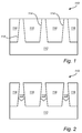
- FIGS 1 to 3 schematically illustrate different process steps according for providing a patterned donor wafer 110 according to an embodiment.
- the donor wafer may be provided by means of a technique known as aspect ratio trapping (ART), which involves high aspect ratio sub-micron trenches to trap threading dislocations, thereby reducing the dislocation density of lattice mismatched materials grown on silicon.
- ART aspect ratio trapping
- a semiconductor substrate 112 may be provided, comprising a first semiconductor material 112 such as e.g. Si.
- Isolation regions, such as shallow trench isolation (STI) regions 116 may be provided, defining fins or lines 114 extending between the STI regions 116.
- the forming of the STI regions 116 may include patterning and etching of the substrate 112 and filling the etched regions with an insulating material such as for example SiO 2 .
- the fins 114 may have a height corresponding to the height (or depth) of the STI regions 116, such as e.g. between 100 nm to 500 nanometres, and a width ranging from 200 nm down to 20 nm or even 5 nm, more preferably ranging from 100 nm down to 20 nm or even 5 nm.
- the fins 114 may be formed of a second semiconductor material 115 forming the sacrificial layer 120. It will however be appreciated that the sacrificial layer 120 (and hence the fin structures 114) may be formed of several layers or materials arranged in e.g. a stacked structure.
- the second semiconductor 115 material may e.g. comprise a group IV, a group III-V or a group II-VI semiconductor material.
- the fins 114 may be at least partly etched back, leaving cavities or recesses 118 between the STI regions 116. These recesses 118 may then be re-filled with the second semiconductor material 115 indicated in figure 3 , forming the sacrificial layer 120.
- the sacrificial layer 120 may comprise a release layer 122 for facilitating the removal of the donor wafer 110 from the handling wafer.
- the release layer 122 may e.g. be embedded in the sacrificial layer 120, as indicated in one of the examples given in figure 3 , or added on top of the sacrificial layer 120.
- Figure 4 illustrates a donor wafer 110 wherein an active layer 130 and a bonding layer 132 are formed on the sacrificial layer 120.
- the active layer 130 may e.g. be provided by epitaxial growth, and may comprise a group III-V, a group IV or a group II-VI semiconductor material serving as the active regions or channel regions of the final semiconductor device.
- Different regions of the sacrificial layer 120 may be provided with different types of active layer 130 materials. In one example, the different regions may correspond to different fins 114 of the donor substrate 112. Some of the regions may then be provided with e.g. an InP layer, whereas other regions may be provided with a Ge layer.
- Such co-integration of different semiconductor materials allows for the InP regions to be used for an NMOS device and the Ge regions to be used for a PMOS device.
- the donor wafer may further be provided with a release layer 122.
- the release layer 122 may e.g. be arranged between the sacrificial layer 120 and the active layer 122 (as illustrated in the middle structure of the sacrificial layer in figure 4 ), or embedded in the sacrificial layer 120 (as indicated in the rightmost structure of the sacrificial layer in figure 4 ).
- the bonding layer 132 may be formed on the active layer 130 so as to facilitate the subsequent bonding to the handling layer.
- the bonding layer 132 may in one example be an Al 2 O 3 /SiO deposited by e.g. chemical vapour deposition (CVD) or atomic layer deposition (ALD) or another bonding material as known to a person skilled in the art.
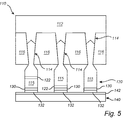
- Figure 5 illustrates the donor wafer 110 (now turned upside down) bonded to a handling wafer 140.
- the handling wafer may be a Si based substrate, such as a blanket Si wafer or a previously patterned Si wafer with Si active and/or Ge, SiGe active regions or e.g. a Ge-on-Si (patterned or blanket) wafer, or a Ge-OI on Si (patterned or blanket) wafer.
- the handling wafer 140 and the donor wafer 110 may be bonded to each other by contacting the bonding layer 132 of the donor wafer 110 to the handling wafer 140, or, if present, to a corresponding bonding layer 142 of the handling wafer 140.
- the donor wafer 110 may be removed from the handling wafer 140 in a lift-off process leaving the active layer 130 on the handling wafer 140.
- the lift-off may be performed by selectively etching at least part of the sacrificial layer 120, e.g. in a dry etch process, until the donor wafer 110 can be released from the handling wafer 140.
- the sacrificial layer 120 may be etched in a manner that allows for the donor wafer 140 to be reused in the processing of subsequent semiconductor devices.
- the sacrificial layer 120 may be removed completely such that the recesses 118 are exposed (cf. figure 2 ).
- the lift-off process may leave at least some of the second material 115 between the fins 116 of the donor substrate 112.
- Other lift-off processes are however conceivable, e.g. including breaking off the donor wafer 110 from the handling wafer 140, preferable at the narrowest portion of the sacrificial layer (as indicated in e.g. figure 6 ). Further examples may include etching a release layer (not shown in figure 6 ) that may be formed in the sacrificial 120 layer or between the sacrificial layer 120 and the active layer 130.
- the lift-off may leave at least some of the material of the sacrificial layer on the active layer (as indicated in the leftmost example of the active layer in figure 6 ).
- the remaining material of the sacrificial layer 120 may be removed in a subsequent etching or planarization process.
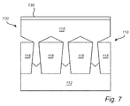
- Figure 7 illustrates a donor wafer 110 according to an embodiment that may be similarly configured embodiment described with reference to figure 4 .
- the sacrificial layer 120 may be grown out of the trenches between the isolation regions 116 such that the fin structure is closed or merged into a substantially continuous layer covering the underlying isolation regions 116. This advantageously allows for a substantially continuous, or non-patterned, active layer 130 to be formed on the sacrificial layer 120.
- the type of sacrificial layer 120 discussed in connection with the above embodiments may be selected based on the type of active layer 130 to be transferred to the handling wafer 140. Some conceivable examples, allowing for a selective etching of the sacrificial layer 120, are listed below:
- the term 'active material' may relate to other materials than channel materials, such as e.g. materials for laser applications, detectors, modulators etcetera.
- the active layer may be strained so as to achieve a desired materials characteristic. The strain may be defined by the specific combination of active material and sacrificial layer.
- Examples of selective etching may include the following processes:
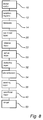
- the method may comprise the steps of providing 10 a donor wafer by forming 12 isolation regions in a donor substrate, and forming fins between the STI regions by recessing 14 at least a portion of the first semiconductor material between the STI regions and forming 20 a sacrificial layer of a second semiconductor material on the donor wafer wherein the forming may include a step of forming 22 a release layer that may be embedded in the sacrificial layer.
- the method may also include a step of forming 30 an active layer on the sacrificial layer, including a planarization process wherein a dielectric layer may be formed 32 on the active layer and planarized 34 prior to the forming 36 of the bonding layer.
- the donor wafer may be removed from the handling wafer by means of e.g. a lift-off step 50, wherein the sacrificial layer may be selectively etched or broken such that the active layer is transferred to the handling wafer.
Landscapes
- Element Separation (AREA)
- Recrystallisation Techniques (AREA)
Abstract
Description
- The present invention relates to the manufacturing of semiconductor devices with an active channel or active layer comprising a group IV or group III-V semiconductor material. Additionally, the present invention relates to a donor wafer for providing such an active region.
- There is a growing interest in materials other than silicon (Si) as active channel material. Possible candidates for replacing Si are e.g. germanium (Ge), which is a group IV material, and III-V materials such as e.g. GaAs, InGaAs or InAs. To be competitive, these should be integrated on a Si platform in order to benefit from the existing Si-based semiconductor processing technologies. The integration of III-V on a Si platform may however be challenging due to crystalline defects such as e.g. lattice mismatch, anti-phase boundaries, mismatch stress relaxation, threading dislocations etcetera.
-
EP 2 924 722 A1 discloses a method for forming such III-V structures on an insulator wafer, wherein a pre-patterned donor wafer is used for transferring channel regions of a group III-V semiconductor material to a Si handling wafer. The group III-V material is provided in fins arranged between shallow trench isolation (STI) regions in a front side of the donor wafer, and is bonded to the handling wafer by means of a bonding oxide layer. The donor wafer is then removed from its back side by e.g. thinning, leaving channel regions of the group III-V semiconductor material on the handling wafer. - Although different methods for manufacturing semiconductor devices as described above are known, there is a need for alternative and improved methods for providing semiconductor devices having an active layer of a group IV or group III-V material.
- It is an object of the present invention to provide an improved methodology for manufacturing semiconductor devices, and in particular to provide a method and a semiconductor wafer for manufacturing a device having an active layer of a group IV material, a group III-V material or a group II-VI material.
- This and other objects of the technology disclosed are achieved by means of a method having the features defined in the independent claim. Different implementations of the technology disclosed are defined in the dependent claims.
- Hence, according to an aspect a method for manufacturing a semiconductor device is provided. In the method, a donor wafer is provided that comprises a first semiconductor material. On this wafer, a sacrificial layer is formed, which comprises a second semiconductor material forming a pattern of fins that are separated from each other by isolation regions such as e.g. shallow trench isolation, STI, regions. The second semiconductor material may be different from the first semiconductor material. Further, an active layer is formed on the sacrificial layer. The active layer may comprise a group IV semiconductor material, a group III-V semiconductor material or a group II-VI semiconductor material. The active layer is then bonded to a handling wafer, and the donor wafer lifted off from the handling wafer, leaving the active layer bonded to the handling wafer.
- The present invention makes use of an understanding that by removing the donor wafer by means of a sacrificial layer, the risk of damaging the active layer may be reduced and the donor wafer reused. The donor wafer may e.g. be lifted off by means of a selective etching of at least a part of the sacrificial layer or by breaking or splitting the sacrificial layer such that the donor wafer can be broken off from the handling wafer. The advantages of using the sacrificial layer could be compared to prior art technologies such as e.g. the "smartcut" process, which involves the implantation of hydrogen to a predetermined depth into the donor wafer prior to the step of bonding, and thereafter releasing the donor wafer at the predetermined depth of the hydrogen implantation by means of an anneal process. The present disclosure is also advantageous over the thinning process, wherein the donor wafer is removed from its back side by means of e.g. grinding. Lifting off the donor wafer by means of the sacrificial layer allows for the donor wafer to be removed without involving any ion-implantation or annealing required e.g. by the smartcut process, thereby reducing the risk of ion-induced damages and diffusion related damages of the active layer. The present aspects are also advantageous over e.g. the thinning process, in which the donor wafer is destroyed in a manner that excludes any reuse and the active layer may be damaged by mechanical stress induced by the grinding. The present invention thus allows for a simpler and more cost efficient process for the donor wafer removal, requiring less processing steps and reducing the risk of damaging the active layer.
- The handling wafer or substrate may be blanket or patterned, and may e.g. be chosen from a Si wafer, a Ge wafer, a germanium-on-silicon wafer, a GeOI wafer, or a III-V on insulator wafer such as e.g. InGaAsOI.
- The donor wafer may be a pre-patterned wafer (e.g. using an ART process for manufacturing thereof) onto which the material of the active layer may be grown only on certain areas of the wafer, thereby reducing costs compared to prior art techniques wherein III-V material is provided over the whole wafer. Further, providing the active layer in fin-shaped or confined areas, instead of a coherent wafer-scaled layer, may reduce the risk of cracking and allows for an increased transfer yield.
- The III-V material may be integrated on the handling wafer monolithically without the use of expensive and small III-V wafers and/or without the use of expensive and thick strain relaxed buffer (SRB)-based substrate.
- According to an embodiment, the step of providing the donor wafer may include a forming of the isolation regions. The isolation regions may be formed in a substrate, such as a blanket Si wafer, comprising the first semiconductor material. The isolating material of the isolation regions may e.g. comprise an oxide such as SiO2. Further, the fins may be formed between the isolation regions, such that at least a top portion of the fins may comprise the second semiconductor material. Thus, the fins may extend from the donor substrate and be separated by, and in between, the isolation regions.
- According to an embodiment, the fins may be formed by recessing at least a portion of the first semiconductor material between the isolation regions. The fins may thus be formed by replacing at least part of the first semiconductor material, either partially (not reaching the depth of the isolation structures) or completely (reaching the full depth of the isolation structures). The removal may be performed by means of etching.
- According to an embodiment, the fins may be formed by growing the second semiconductor material, e.g. by epitaxial growth, starting from the first semiconductor material.
- The mechanism of replacing the first semiconductor material into the second semiconductor material may also be referred to as aspect ratio trapping (ART) technique, which is advantageous in that may reduce the formation of defects during such a regrowth process.
- According to an embodiment, the first semiconductor material may be silicon. It will also be appreciated that the second semiconductor material of the fins may be a group III-V, a group II-VI or a group IV semiconductor material, and that the sacrificial layer may be formed of the same second semiconductor material or a material that is different from the second semiconductor material. The sacrificial layer may be integrally formed with the second semiconductor material of the fins, or be formed of a stack of a plurality of materials.
- According to an embodiment, the method may comprise a step of forming a release layer for facilitating the removal of the donor wafer from the handling wafer. The release layer may e.g. be embedded in the sacrificial layer, or arranged on top of the sacrificial layer (thus forming an intermediate layer between the sacrificial layer and the active layer). In one example, the release layer may be an ion-implanted hydrogen layer of the type used in the smartcut process.
- According to an embodiment, a dielectric layer may be formed on the active layer. Further, the dielectric layer may be planarised (e.g. by chemical mechanical polishing, CMP), preferably down to the active layer which thereby is exposed. The planarisation may be performed so as to provide a levelled surface of the active layer. After planarisation the dielectric layer may be removed prior to bonding.
- According to an embodiment, a bonding layer may be formed on the active layer of the donor wafer. Alternatively, or additionally, the handling wafer may be provided with a similar bonding layer for facilitating the bonding. The choice and presence of a bonding layer may be determined by the particular process used for bonding the donor wafer to the handling wafer. Preferably, the bonding layer is capable of reducing the surface roughness of the surface(s) to be bonded. The bonding layer may e.g. be a dielectric layer, including e.g. insulating metal oxides (e.g. Al2O3, HfO2), insulating dielectrics (e.g. SiO, SiN), and insulating wide bandgap semiconductors (such as AIN).
- According to an embodiment, the donor wafer may be lifted off or removed from the handling wafer in a single piece. This allows for the donor wafer to be reused, e.g. by re-growing the fins between the STI regions, so as to reduce the processing costs. The lift-off may be facilitated by means of a mechanical splitting initiation.
- According to an embodiment, the handling wafer (or the donor wafer) may be a flexible wafer or substrate, which e.g. may be lifted off by means of a break-off process. The flexible wafer may e.g. be released by being guided over a cylinder surface, or pulled off by an applied force. Examples of such wafers, or substrates, include polyimide materials, polyether ether ketone (PEEK), transparent and conductive polyester materials, and thin sheets of glass. Such substrates may e.g. be used in connection with flexible electronics or optoelectronics, which e.g. may be employed in flex circuits, foldable displays and solar panels.
- According to some embodiments, the donor wafer and/or the handling wafer may have a wafer size of at least 300 mm.
- According to some embodiments, the group III-V semiconductor material(s) may be selected from InP, InGaAs, InAs, GaAs, AlAs, GaSb, AlSb, InSb, GaP, AlP, BAs, BP, BSb, GaN, AIN, InN, GaAsSb and ternary and quaternary combinations thereof.
- The group IV semiconductor material may be chosen from Ge, SiGe, SnGe or SnSi.
- Further objectives, features and advantages of the present invention will appear from the following detailed disclosures as well as from the drawings and the appended claims. Those skilled in the art will realise that different features of the present embodiment can be combined to create embodiments other than those described in the following.
- In the following, reference will be made to the appended drawings, on which:
-
figures 1 and 2 are schematic cross sections of a donor wafer at different stages of the manufacturing method according to embodiments of the present invention; -
figure 3 is a schematic cross section illustrating a donor wafer comprising a sacrificial layer according to an embodiment; -
figure 4 is a schematic cross section of the donor wafer offigure 3 , further comprising an active layer and a bonding layer; -
figure 5 schematically illustrates a donor wafer that has been bonded to a handling wafer according to an embodiment; -
figure 6 illustrates the lift-off process of the donor wafer according to an embodiment; -
figure 7 is a schematic cross section of a donor wafer wherein the sacrificial layer is merged into a substantially continuous layer; and -
figure 8 is a schematic illustration of a method according to an embodiment. - All the figures are schematic, not necessarily to scale, and generally only show parts which are necessary in order to elucidate the invention, wherein other parts may be omitted or merely suggested.
-
Figures 1 to 3 schematically illustrate different process steps according for providing a patterneddonor wafer 110 according to an embodiment. The donor wafer may be provided by means of a technique known as aspect ratio trapping (ART), which involves high aspect ratio sub-micron trenches to trap threading dislocations, thereby reducing the dislocation density of lattice mismatched materials grown on silicon. - Firstly, a
semiconductor substrate 112 may be provided, comprising afirst semiconductor material 112 such as e.g. Si. Isolation regions, such as shallow trench isolation (STI)regions 116 may be provided, defining fins orlines 114 extending between theSTI regions 116. The forming of theSTI regions 116 may include patterning and etching of thesubstrate 112 and filling the etched regions with an insulating material such as for example SiO2. Thefins 114 may have a height corresponding to the height (or depth) of theSTI regions 116, such as e.g. between 100 nm to 500 nanometres, and a width ranging from 200 nm down to 20 nm or even 5 nm, more preferably ranging from 100 nm down to 20 nm or even 5 nm. - The
fins 114 may be formed of asecond semiconductor material 115 forming thesacrificial layer 120. It will however be appreciated that the sacrificial layer 120 (and hence the fin structures 114) may be formed of several layers or materials arranged in e.g. a stacked structure. Thesecond semiconductor 115 material may e.g. comprise a group IV, a group III-V or a group II-VI semiconductor material. As indicated infigure 2 , thefins 114 may be at least partly etched back, leaving cavities or recesses 118 between theSTI regions 116. Theserecesses 118 may then be re-filled with thesecond semiconductor material 115 indicated infigure 3 , forming thesacrificial layer 120. According to some embodiments, thesacrificial layer 120 may comprise arelease layer 122 for facilitating the removal of thedonor wafer 110 from the handling wafer. Therelease layer 122 may e.g. be embedded in thesacrificial layer 120, as indicated in one of the examples given infigure 3 , or added on top of thesacrificial layer 120. -
Figure 4 illustrates adonor wafer 110 wherein anactive layer 130 and abonding layer 132 are formed on thesacrificial layer 120. Theactive layer 130 may e.g. be provided by epitaxial growth, and may comprise a group III-V, a group IV or a group II-VI semiconductor material serving as the active regions or channel regions of the final semiconductor device. Different regions of thesacrificial layer 120 may be provided with different types ofactive layer 130 materials. In one example, the different regions may correspond todifferent fins 114 of thedonor substrate 112. Some of the regions may then be provided with e.g. an InP layer, whereas other regions may be provided with a Ge layer. Such co-integration of different semiconductor materials allows for the InP regions to be used for an NMOS device and the Ge regions to be used for a PMOS device. - As indicated in
figure 4 , the donor wafer may further be provided with arelease layer 122. Therelease layer 122 may e.g. be arranged between thesacrificial layer 120 and the active layer 122 (as illustrated in the middle structure of the sacrificial layer infigure 4 ), or embedded in the sacrificial layer 120 (as indicated in the rightmost structure of the sacrificial layer infigure 4 ). - The
bonding layer 132 may be formed on theactive layer 130 so as to facilitate the subsequent bonding to the handling layer. Thebonding layer 132 may in one example be an Al2O3/SiO deposited by e.g. chemical vapour deposition (CVD) or atomic layer deposition (ALD) or another bonding material as known to a person skilled in the art. -
Figure 5 illustrates the donor wafer 110 (now turned upside down) bonded to ahandling wafer 140. The handling wafer may be a Si based substrate, such as a blanket Si wafer or a previously patterned Si wafer with Si active and/or Ge, SiGe active regions or e.g. a Ge-on-Si (patterned or blanket) wafer, or a Ge-OI on Si (patterned or blanket) wafer. - The handling
wafer 140 and thedonor wafer 110 may be bonded to each other by contacting thebonding layer 132 of thedonor wafer 110 to thehandling wafer 140, or, if present, to acorresponding bonding layer 142 of thehandling wafer 140. - As indicated in
figure 6 , thedonor wafer 110 may be removed from the handlingwafer 140 in a lift-off process leaving theactive layer 130 on thehandling wafer 140. The lift-off may be performed by selectively etching at least part of thesacrificial layer 120, e.g. in a dry etch process, until thedonor wafer 110 can be released from the handlingwafer 140. Thesacrificial layer 120 may be etched in a manner that allows for thedonor wafer 140 to be reused in the processing of subsequent semiconductor devices. During the lift-off thesacrificial layer 120 may be removed completely such that therecesses 118 are exposed (cf.figure 2 ). Alternatively, the lift-off process may leave at least some of thesecond material 115 between thefins 116 of thedonor substrate 112. Other lift-off processes are however conceivable, e.g. including breaking off thedonor wafer 110 from the handlingwafer 140, preferable at the narrowest portion of the sacrificial layer (as indicated in e.g.figure 6 ). Further examples may include etching a release layer (not shown infigure 6 ) that may be formed in the sacrificial 120 layer or between thesacrificial layer 120 and theactive layer 130. In case the release layer is embedded in thesacrificial layer 120, the lift-off may leave at least some of the material of the sacrificial layer on the active layer (as indicated in the leftmost example of the active layer infigure 6 ). The remaining material of thesacrificial layer 120 may be removed in a subsequent etching or planarization process. -
Figure 7 illustrates adonor wafer 110 according to an embodiment that may be similarly configured embodiment described with reference tofigure 4 . As indicated in the figure, thesacrificial layer 120 may be grown out of the trenches between theisolation regions 116 such that the fin structure is closed or merged into a substantially continuous layer covering theunderlying isolation regions 116. This advantageously allows for a substantially continuous, or non-patterned,active layer 130 to be formed on thesacrificial layer 120. - The type of
sacrificial layer 120 discussed in connection with the above embodiments may be selected based on the type ofactive layer 130 to be transferred to thehandling wafer 140. Some conceivable examples, allowing for a selective etching of thesacrificial layer 120, are listed below: - sacrificial layer: InP, active layer: GaInAs;
- sacrificial layer: InP, active layer: GaSbAs;
- sacrificial layer: GaInAs, active layer: InP;
- sacrificial layer: GaInAs, active layer: GeSn;
- sacrificial layer: InAs, active layer: GaSb;
- sacrificial layer: GaSb, active layer: InAs;
- sacrificial layer: GaAs, active layer: Ge;
- sacrificial layer: Ga, active layer: GaAs;
- sacrificial layer: GeSi, active layer: GaPAs;
- sacrificial layer: BGaP, active layer: Si;
- sacrificial layer: GaPN, active layer: Si;
- sacrificial layer: GaAsP, active layer: SiGe.
- It will however be appreciated the term 'active material' may relate to other materials than channel materials, such as e.g. materials for laser applications, detectors, modulators etcetera. Further, the active layer may be strained so as to achieve a desired materials characteristic. The strain may be defined by the specific combination of active material and sacrificial layer.
- Examples of selective etching may include the following processes:
- InGaAs or InAlAs selectively removed from InP by means of H2SO4:H2O2:H2O or H3PO4:H2O2:H2O in a wet or vapour etching process.
- InAs selectively removed from InP by means of HF:H2O or HNO3:H2O2
- GaSb may be selectively removed from InP by means of CH3COOH:HN03:HF followed by HCl:HNO3:H2O2
- GaSb selectively removed from InAs by means of HF:H2O2:H2O, wherein InAs may act as a stop layer
- GaAs selectively removed from Ge by means of H2SO4:H2O2:H2O, or by XeF2 in a dry etching process
- GaP selectively removed from Si by means of aqua regia, 1:1 or 3:1 (HCl:HNO3) or 1:1:1 (HCl:HNO3:CH3COOH).
- With reference to
figure 8 there is illustrated a schematic outline of a method for manufacturing a semiconductor device according to an embodiment. The method may comprise the steps of providing 10 a donor wafer by forming 12 isolation regions in a donor substrate, and forming fins between the STI regions by recessing 14 at least a portion of the first semiconductor material between the STI regions and forming 20 a sacrificial layer of a second semiconductor material on the donor wafer wherein the forming may include a step of forming 22 a release layer that may be embedded in the sacrificial layer. The method may also include a step of forming 30 an active layer on the sacrificial layer, including a planarization process wherein a dielectric layer may be formed 32 on the active layer and planarized 34 prior to the forming 36 of the bonding layer. After thebonding step 40, the donor wafer may be removed from the handling wafer by means of e.g. a lift-off step 50, wherein the sacrificial layer may be selectively etched or broken such that the active layer is transferred to the handling wafer.
Claims (14)
- A method for manufacturing a semiconductor device (100), comprising:providing (10) a donor wafer (110) comprising a first semiconductor material (112);forming (20) a sacrificial layer (120) on the donor wafer, the sacrificial layer comprising a second semiconductor material (115) forming a pattern of fins (114) separated from each other by isolation regions (116);forming (30) an active layer (130) on the sacrificial layer, the active layer comprising a group IV semiconductor material or a group III-V semiconductor material or a group II-VI semiconductor material;bonding (40) the active layer to a handling wafer (140);lifting off (50) the donor wafer from the handling wafer such that the active layer is left on the handling wafer.
- The method according to claim 1, wherein providing the donor wafer comprises:forming (12) the isolation regions in a donor substrate comprising the first semiconductor material; andforming (14) fins between the isolation regions, wherein at least a top portion of the fins comprises the second semiconductor material.
- The method according to claim 1, wherein the sacrificial layer comprises a group III-V or a group II-VI or a group IV material being different from the material of the active layer.
- The method according to claims 1 to 3, wherein the first semiconductor material is silicon and/or the second semiconductor material is a group III-V or a group II-VI or a group IV semiconductor material.
- The method according to any one of the preceding claims, further comprising forming (22) a release layer (122) on the sacrificial layer, wherein the step of lifting off the donor wafer comprises selectively etching the release layer.
- The method according to any one of claims 1 to 4, wherein forming the sacrificial layer further comprises:forming (22) a release layer that is embedded in the sacrificial layer;lifting off the donor wafer by selectively etching the release layer; andselectively removing the remaining portions of the sacrificial layer from the active layer.
- The method according to any one of the preceding claims, further comprising, before bonding the active layer to the handling wafer:forming (32) a dielectric layer on the active layer; andplanarising (34) the dielectric layer.
- The method according to any one of the preceding claims, wherein bonding the active layer further comprises:forming (36) a bonding layer (132) on the active layer;wherein the active layer is bonded to the handling wafer by means of the bonding layer.
- The method according to any one of the preceding claims, wherein the active layer is bonded by means of a bonding layer (142) of the handling layer.
- The method according to any one of the preceding claims, wherein the donor wafer is lifted off from the handling wafer by means of selectively etching of at least a part of the sacrificial layer.
- The method according to claim 1, wherein the donor wafer is lifted off from the handling wafer by means of breaking off the donor wafer from the handling wafer.
- The method according to any one of the preceding claims, wherein the donor wafer is lifted off in a single piece.
- The method according to any one of the preceding claims, wherein the handling wafer is a flexible wafer.
- The method according to any one of the preceding claims, wherein:the sacrificial layer comprises InP and the active layer comprises GaInAs; orthe sacrificial layer comprises InP and the active layer comprises GaSbAs; orthe sacrificial layer comprises GaInAs and the active layer comprises InP; orthe sacrificial layer comprises GaInAs and the active layer comprises GeSn; orthe sacrificial layer comprises InAs and the active layer comprises GaSb;orthe sacrificial layer comprises GaSb and the active layer comprises InAs;orthe sacrificial layer comprises GaAs and the active layer comprises Ge; orthe sacrificial layer comprises Ga and the active layer comprises GaAs; orthe sacrificial layer comprises GeSi and the active layer comprises GaPAs;orthe sacrificial layer comprises BGaP and the active layer comprises Si; orthe sacrificial layer comprises GaPN and the active layer comprises Si; orthe sacrificial layer comprises GaAsP and the active layer comprises SiGe.
Priority Applications (2)
| Application Number | Priority Date | Filing Date | Title |
|---|---|---|---|
| EP16185708.1A EP3288067B1 (en) | 2016-08-25 | 2016-08-25 | Method for transferring a group iii-iv semiconductor active layer |
| US15/687,304 US10340188B2 (en) | 2016-08-25 | 2017-08-25 | Method of transferring a semiconductor layer |
Applications Claiming Priority (1)
| Application Number | Priority Date | Filing Date | Title |
|---|---|---|---|
| EP16185708.1A EP3288067B1 (en) | 2016-08-25 | 2016-08-25 | Method for transferring a group iii-iv semiconductor active layer |
Publications (2)
| Publication Number | Publication Date |
|---|---|
| EP3288067A1 true EP3288067A1 (en) | 2018-02-28 |
| EP3288067B1 EP3288067B1 (en) | 2021-10-27 |
Family
ID=56893700
Family Applications (1)
| Application Number | Title | Priority Date | Filing Date |
|---|---|---|---|
| EP16185708.1A Active EP3288067B1 (en) | 2016-08-25 | 2016-08-25 | Method for transferring a group iii-iv semiconductor active layer |
Country Status (2)
| Country | Link |
|---|---|
| US (1) | US10340188B2 (en) |
| EP (1) | EP3288067B1 (en) |
Cited By (3)
| Publication number | Priority date | Publication date | Assignee | Title |
|---|---|---|---|---|
| CN113690190A (en) * | 2020-05-18 | 2021-11-23 | Imec 非营利协会 | III-V architecture integration on group IV substrates |
| EP4287247A1 (en) | 2022-06-02 | 2023-12-06 | Imec VZW | A method for producing a semiconductor chip |
| WO2025230716A1 (en) * | 2024-04-29 | 2025-11-06 | Qualcomm Incorporated | Impure indium phosphide semiconductor substrate on a silicon wafer |
Families Citing this family (1)
| Publication number | Priority date | Publication date | Assignee | Title |
|---|---|---|---|---|
| GB2593864B (en) * | 2020-02-28 | 2023-01-04 | X Fab France Sas | Improved transfer printing for RF applications |
Citations (7)
| Publication number | Priority date | Publication date | Assignee | Title |
|---|---|---|---|---|
| JP2001102668A (en) * | 1999-09-28 | 2001-04-13 | Kyocera Corp | Semiconductor substrate manufacturing method |
| US20070054465A1 (en) * | 2005-09-07 | 2007-03-08 | Amberwave Systems Corporation | Lattice-mismatched semiconductor structures on insulators |
| US20130214284A1 (en) * | 2012-02-17 | 2013-08-22 | The Regents Of The University Of California | Method for the reuse of gallium nitride epitaxial substrates |
| US20150137187A1 (en) * | 2012-07-24 | 2015-05-21 | Sumitomo Chemical Company, Limited | Semiconductor wafer, manufacturing method of semiconductor wafer and method for maunfacturing composite wafer |
| US20150162403A1 (en) * | 2013-12-10 | 2015-06-11 | Taiwan Semiconductor Manufacturing Company Limited | Replacement gate nanowire device |
| US20150179664A1 (en) * | 2013-12-24 | 2015-06-25 | Alejandro X. Levander | Heterogeneous semiconductor material integration techniques |
| EP2924722A1 (en) | 2014-03-28 | 2015-09-30 | IMEC vzw | Method for manufacturing a semiconductor-on-insulator device |
Family Cites Families (11)
| Publication number | Priority date | Publication date | Assignee | Title |
|---|---|---|---|---|
| US7279369B2 (en) | 2003-08-21 | 2007-10-09 | Intel Corporation | Germanium on insulator fabrication via epitaxial germanium bonding |
| US20060234474A1 (en) | 2005-04-15 | 2006-10-19 | The Regents Of The University Of California | Method of transferring a thin crystalline semiconductor layer |
| US8098612B2 (en) * | 2007-05-21 | 2012-01-17 | Spatial Digital Systems, Inc. | Apparatus and method for remote beam forming for satellite broadcasting systems |
| US8735191B2 (en) | 2012-01-04 | 2014-05-27 | Skorpios Technologies, Inc. | Method and system for template assisted wafer bonding using pedestals |
| EP2686878B1 (en) | 2011-03-16 | 2016-05-18 | MEMC Electronic Materials, Inc. | Silicon on insulator structures having high resistivity regions in the handle wafer and methods for producing such structures |
| FR2975222A1 (en) | 2011-05-10 | 2012-11-16 | Soitec Silicon On Insulator | PROCESS FOR PRODUCING A SEMICONDUCTOR SUBSTRATE |
| US8741739B2 (en) | 2012-01-03 | 2014-06-03 | International Business Machines Corporation | High resistivity silicon-on-insulator substrate and method of forming |
| US9000557B2 (en) | 2012-03-17 | 2015-04-07 | Zvi Or-Bach | Semiconductor device and structure |
| US9257339B2 (en) | 2012-05-04 | 2016-02-09 | Silicon Genesis Corporation | Techniques for forming optoelectronic devices |
| US9386842B2 (en) * | 2013-07-11 | 2016-07-12 | David Scott Doherty | Broom with hooked bristles section |
| US9355889B2 (en) * | 2014-03-28 | 2016-05-31 | Imec Vzw | Semiconductor-on-insulator device and method of fabricating the same |
-
2016
- 2016-08-25 EP EP16185708.1A patent/EP3288067B1/en active Active
-
2017
- 2017-08-25 US US15/687,304 patent/US10340188B2/en active Active
Patent Citations (7)
| Publication number | Priority date | Publication date | Assignee | Title |
|---|---|---|---|---|
| JP2001102668A (en) * | 1999-09-28 | 2001-04-13 | Kyocera Corp | Semiconductor substrate manufacturing method |
| US20070054465A1 (en) * | 2005-09-07 | 2007-03-08 | Amberwave Systems Corporation | Lattice-mismatched semiconductor structures on insulators |
| US20130214284A1 (en) * | 2012-02-17 | 2013-08-22 | The Regents Of The University Of California | Method for the reuse of gallium nitride epitaxial substrates |
| US20150137187A1 (en) * | 2012-07-24 | 2015-05-21 | Sumitomo Chemical Company, Limited | Semiconductor wafer, manufacturing method of semiconductor wafer and method for maunfacturing composite wafer |
| US20150162403A1 (en) * | 2013-12-10 | 2015-06-11 | Taiwan Semiconductor Manufacturing Company Limited | Replacement gate nanowire device |
| US20150179664A1 (en) * | 2013-12-24 | 2015-06-25 | Alejandro X. Levander | Heterogeneous semiconductor material integration techniques |
| EP2924722A1 (en) | 2014-03-28 | 2015-09-30 | IMEC vzw | Method for manufacturing a semiconductor-on-insulator device |
Cited By (6)
| Publication number | Priority date | Publication date | Assignee | Title |
|---|---|---|---|---|
| CN113690190A (en) * | 2020-05-18 | 2021-11-23 | Imec 非营利协会 | III-V architecture integration on group IV substrates |
| EP3913655A1 (en) * | 2020-05-18 | 2021-11-24 | IMEC vzw | Integration of a iii-v construction on a group iv substrate |
| US11646200B2 (en) | 2020-05-18 | 2023-05-09 | Imec Vzw | Integration of a III-V construction on a group IV substrate |
| CN113690190B (en) * | 2020-05-18 | 2026-04-24 | Imec非营利协会 | III-V structure integrated on a group IV substrate |
| EP4287247A1 (en) | 2022-06-02 | 2023-12-06 | Imec VZW | A method for producing a semiconductor chip |
| WO2025230716A1 (en) * | 2024-04-29 | 2025-11-06 | Qualcomm Incorporated | Impure indium phosphide semiconductor substrate on a silicon wafer |
Also Published As
| Publication number | Publication date |
|---|---|
| EP3288067B1 (en) | 2021-10-27 |
| US10340188B2 (en) | 2019-07-02 |
| US20180061712A1 (en) | 2018-03-01 |
Similar Documents
| Publication | Publication Date | Title |
|---|---|---|
| US7790528B2 (en) | Dual substrate orientation or bulk on SOI integrations using oxidation for silicon epitaxy spacer formation | |
| US9355889B2 (en) | Semiconductor-on-insulator device and method of fabricating the same | |
| CN100362618C (en) | A kind of semiconductor device and manufacturing method | |
| US7282425B2 (en) | Structure and method of integrating compound and elemental semiconductors for high-performance CMOS | |
| US11728207B2 (en) | Method for fabricating a strained semiconductor-on-insulator substrate | |
| EP2153462B1 (en) | Method for producing hybrid components | |
| US9570351B2 (en) | Reusable semiconductor substrates | |
| US10340188B2 (en) | Method of transferring a semiconductor layer | |
| EP3459106B1 (en) | Method for fabricating a strained semiconductor-on-insulator substrate | |
| KR101904114B1 (en) | Method for fabricating semiconductor layers including transistor channels having different strain states, and related semiconductor layers | |
| US20080254591A1 (en) | Method for Making a Thin-Film Element | |
| US20060128078A1 (en) | SOI substrate manufacturing method | |
| EP2924722A1 (en) | Method for manufacturing a semiconductor-on-insulator device | |
| US10504771B2 (en) | Semiconductor device including strained germanium and method for manufacturing the same | |
| US12438036B2 (en) | Method for manufacturing a SOI or SiGeOI type semiconductor-on-insulator substrate by BESOI and structure for manufacturing such a substrate | |
| US9048286B2 (en) | Substrate for integrated circuit and method for forming the same | |
| WO2011018780A1 (en) | A process for manufacturing a hybrid substrate | |
| US11295950B2 (en) | Structure comprising single-crystal semiconductor islands and process for making such a structure | |
| US10014374B2 (en) | Planar heterogeneous device | |
| JP2005045115A (en) | Semiconductor device and manufacturing method thereof | |
| EP2779212A2 (en) | Method of forming a high electron mobility semiconductor device | |
| JP2005268697A (en) | Semiconductor substrate manufacturing method and semiconductor device manufacturing method | |
| KR20180130792A (en) | Semicondutor device with horizontally aligned semiconductor channels and method for manufacturing the same |
Legal Events
| Date | Code | Title | Description |
|---|---|---|---|
| PUAI | Public reference made under article 153(3) epc to a published international application that has entered the european phase |
Free format text: ORIGINAL CODE: 0009012 |
|
| STAA | Information on the status of an ep patent application or granted ep patent |
Free format text: STATUS: THE APPLICATION HAS BEEN PUBLISHED |
|
| AK | Designated contracting states |
Kind code of ref document: A1 Designated state(s): AL AT BE BG CH CY CZ DE DK EE ES FI FR GB GR HR HU IE IS IT LI LT LU LV MC MK MT NL NO PL PT RO RS SE SI SK SM TR |
|
| AX | Request for extension of the european patent |
Extension state: BA ME |
|
| STAA | Information on the status of an ep patent application or granted ep patent |
Free format text: STATUS: REQUEST FOR EXAMINATION WAS MADE |
|
| RBV | Designated contracting states (corrected) |
Designated state(s): AL AT BE BG CH CY CZ DE DK EE ES FI FR GB GR HR HU IE IS IT LI LT LU LV MC MK MT NL NO PL PT RO RS SE SI SK SM TR |
|
| 17P | Request for examination filed |
Effective date: 20180828 |
|
| STAA | Information on the status of an ep patent application or granted ep patent |
Free format text: STATUS: EXAMINATION IS IN PROGRESS |
|
| 17Q | First examination report despatched |
Effective date: 20200312 |
|
| GRAP | Despatch of communication of intention to grant a patent |
Free format text: ORIGINAL CODE: EPIDOSNIGR1 |
|
| STAA | Information on the status of an ep patent application or granted ep patent |
Free format text: STATUS: GRANT OF PATENT IS INTENDED |
|
| INTG | Intention to grant announced |
Effective date: 20210616 |
|
| GRAS | Grant fee paid |
Free format text: ORIGINAL CODE: EPIDOSNIGR3 |
|
| GRAA | (expected) grant |
Free format text: ORIGINAL CODE: 0009210 |
|
| STAA | Information on the status of an ep patent application or granted ep patent |
Free format text: STATUS: THE PATENT HAS BEEN GRANTED |
|
| AK | Designated contracting states |
Kind code of ref document: B1 Designated state(s): AL AT BE BG CH CY CZ DE DK EE ES FI FR GB GR HR HU IE IS IT LI LT LU LV MC MK MT NL NO PL PT RO RS SE SI SK SM TR |
|
| REG | Reference to a national code |
Ref country code: GB Ref legal event code: FG4D |
|
| REG | Reference to a national code |
Ref country code: CH Ref legal event code: EP |
|
| REG | Reference to a national code |
Ref country code: AT Ref legal event code: REF Ref document number: 1442601 Country of ref document: AT Kind code of ref document: T Effective date: 20211115 |
|
| REG | Reference to a national code |
Ref country code: DE Ref legal event code: R096 Ref document number: 602016065337 Country of ref document: DE |
|
| REG | Reference to a national code |
Ref country code: IE Ref legal event code: FG4D |
|
| REG | Reference to a national code |
Ref country code: LT Ref legal event code: MG9D |
|
| REG | Reference to a national code |
Ref country code: NL Ref legal event code: MP Effective date: 20211027 |
|
| REG | Reference to a national code |
Ref country code: AT Ref legal event code: MK05 Ref document number: 1442601 Country of ref document: AT Kind code of ref document: T Effective date: 20211027 |
|
| PG25 | Lapsed in a contracting state [announced via postgrant information from national office to epo] |
Ref country code: RS Free format text: LAPSE BECAUSE OF FAILURE TO SUBMIT A TRANSLATION OF THE DESCRIPTION OR TO PAY THE FEE WITHIN THE PRESCRIBED TIME-LIMIT Effective date: 20211027 Ref country code: LT Free format text: LAPSE BECAUSE OF FAILURE TO SUBMIT A TRANSLATION OF THE DESCRIPTION OR TO PAY THE FEE WITHIN THE PRESCRIBED TIME-LIMIT Effective date: 20211027 Ref country code: FI Free format text: LAPSE BECAUSE OF FAILURE TO SUBMIT A TRANSLATION OF THE DESCRIPTION OR TO PAY THE FEE WITHIN THE PRESCRIBED TIME-LIMIT Effective date: 20211027 Ref country code: BG Free format text: LAPSE BECAUSE OF FAILURE TO SUBMIT A TRANSLATION OF THE DESCRIPTION OR TO PAY THE FEE WITHIN THE PRESCRIBED TIME-LIMIT Effective date: 20220127 Ref country code: AT Free format text: LAPSE BECAUSE OF FAILURE TO SUBMIT A TRANSLATION OF THE DESCRIPTION OR TO PAY THE FEE WITHIN THE PRESCRIBED TIME-LIMIT Effective date: 20211027 |
|
| PG25 | Lapsed in a contracting state [announced via postgrant information from national office to epo] |
Ref country code: IS Free format text: LAPSE BECAUSE OF FAILURE TO SUBMIT A TRANSLATION OF THE DESCRIPTION OR TO PAY THE FEE WITHIN THE PRESCRIBED TIME-LIMIT Effective date: 20220227 Ref country code: SE Free format text: LAPSE BECAUSE OF FAILURE TO SUBMIT A TRANSLATION OF THE DESCRIPTION OR TO PAY THE FEE WITHIN THE PRESCRIBED TIME-LIMIT Effective date: 20211027 Ref country code: PT Free format text: LAPSE BECAUSE OF FAILURE TO SUBMIT A TRANSLATION OF THE DESCRIPTION OR TO PAY THE FEE WITHIN THE PRESCRIBED TIME-LIMIT Effective date: 20220228 Ref country code: PL Free format text: LAPSE BECAUSE OF FAILURE TO SUBMIT A TRANSLATION OF THE DESCRIPTION OR TO PAY THE FEE WITHIN THE PRESCRIBED TIME-LIMIT Effective date: 20211027 Ref country code: NO Free format text: LAPSE BECAUSE OF FAILURE TO SUBMIT A TRANSLATION OF THE DESCRIPTION OR TO PAY THE FEE WITHIN THE PRESCRIBED TIME-LIMIT Effective date: 20220127 Ref country code: NL Free format text: LAPSE BECAUSE OF FAILURE TO SUBMIT A TRANSLATION OF THE DESCRIPTION OR TO PAY THE FEE WITHIN THE PRESCRIBED TIME-LIMIT Effective date: 20211027 Ref country code: LV Free format text: LAPSE BECAUSE OF FAILURE TO SUBMIT A TRANSLATION OF THE DESCRIPTION OR TO PAY THE FEE WITHIN THE PRESCRIBED TIME-LIMIT Effective date: 20211027 Ref country code: HR Free format text: LAPSE BECAUSE OF FAILURE TO SUBMIT A TRANSLATION OF THE DESCRIPTION OR TO PAY THE FEE WITHIN THE PRESCRIBED TIME-LIMIT Effective date: 20211027 Ref country code: GR Free format text: LAPSE BECAUSE OF FAILURE TO SUBMIT A TRANSLATION OF THE DESCRIPTION OR TO PAY THE FEE WITHIN THE PRESCRIBED TIME-LIMIT Effective date: 20220128 Ref country code: ES Free format text: LAPSE BECAUSE OF FAILURE TO SUBMIT A TRANSLATION OF THE DESCRIPTION OR TO PAY THE FEE WITHIN THE PRESCRIBED TIME-LIMIT Effective date: 20211027 |
|
| REG | Reference to a national code |
Ref country code: DE Ref legal event code: R097 Ref document number: 602016065337 Country of ref document: DE |
|
| PG25 | Lapsed in a contracting state [announced via postgrant information from national office to epo] |
Ref country code: SM Free format text: LAPSE BECAUSE OF FAILURE TO SUBMIT A TRANSLATION OF THE DESCRIPTION OR TO PAY THE FEE WITHIN THE PRESCRIBED TIME-LIMIT Effective date: 20211027 Ref country code: SK Free format text: LAPSE BECAUSE OF FAILURE TO SUBMIT A TRANSLATION OF THE DESCRIPTION OR TO PAY THE FEE WITHIN THE PRESCRIBED TIME-LIMIT Effective date: 20211027 Ref country code: RO Free format text: LAPSE BECAUSE OF FAILURE TO SUBMIT A TRANSLATION OF THE DESCRIPTION OR TO PAY THE FEE WITHIN THE PRESCRIBED TIME-LIMIT Effective date: 20211027 Ref country code: EE Free format text: LAPSE BECAUSE OF FAILURE TO SUBMIT A TRANSLATION OF THE DESCRIPTION OR TO PAY THE FEE WITHIN THE PRESCRIBED TIME-LIMIT Effective date: 20211027 Ref country code: DK Free format text: LAPSE BECAUSE OF FAILURE TO SUBMIT A TRANSLATION OF THE DESCRIPTION OR TO PAY THE FEE WITHIN THE PRESCRIBED TIME-LIMIT Effective date: 20211027 Ref country code: CZ Free format text: LAPSE BECAUSE OF FAILURE TO SUBMIT A TRANSLATION OF THE DESCRIPTION OR TO PAY THE FEE WITHIN THE PRESCRIBED TIME-LIMIT Effective date: 20211027 |
|
| PLBE | No opposition filed within time limit |
Free format text: ORIGINAL CODE: 0009261 |
|
| STAA | Information on the status of an ep patent application or granted ep patent |
Free format text: STATUS: NO OPPOSITION FILED WITHIN TIME LIMIT |
|
| 26N | No opposition filed |
Effective date: 20220728 |
|
| PG25 | Lapsed in a contracting state [announced via postgrant information from national office to epo] |
Ref country code: AL Free format text: LAPSE BECAUSE OF FAILURE TO SUBMIT A TRANSLATION OF THE DESCRIPTION OR TO PAY THE FEE WITHIN THE PRESCRIBED TIME-LIMIT Effective date: 20211027 |
|
| PG25 | Lapsed in a contracting state [announced via postgrant information from national office to epo] |
Ref country code: SI Free format text: LAPSE BECAUSE OF FAILURE TO SUBMIT A TRANSLATION OF THE DESCRIPTION OR TO PAY THE FEE WITHIN THE PRESCRIBED TIME-LIMIT Effective date: 20211027 |
|
| PG25 | Lapsed in a contracting state [announced via postgrant information from national office to epo] |
Ref country code: MC Free format text: LAPSE BECAUSE OF FAILURE TO SUBMIT A TRANSLATION OF THE DESCRIPTION OR TO PAY THE FEE WITHIN THE PRESCRIBED TIME-LIMIT Effective date: 20211027 |
|
| REG | Reference to a national code |
Ref country code: CH Ref legal event code: PL |
|
| GBPC | Gb: european patent ceased through non-payment of renewal fee |
Effective date: 20220825 |
|
| PG25 | Lapsed in a contracting state [announced via postgrant information from national office to epo] |
Ref country code: LU Free format text: LAPSE BECAUSE OF NON-PAYMENT OF DUE FEES Effective date: 20220825 Ref country code: LI Free format text: LAPSE BECAUSE OF NON-PAYMENT OF DUE FEES Effective date: 20220831 Ref country code: CH Free format text: LAPSE BECAUSE OF NON-PAYMENT OF DUE FEES Effective date: 20220831 |
|
| REG | Reference to a national code |
Ref country code: BE Ref legal event code: MM Effective date: 20220831 |
|
| PG25 | Lapsed in a contracting state [announced via postgrant information from national office to epo] |
Ref country code: IT Free format text: LAPSE BECAUSE OF FAILURE TO SUBMIT A TRANSLATION OF THE DESCRIPTION OR TO PAY THE FEE WITHIN THE PRESCRIBED TIME-LIMIT Effective date: 20211027 |
|
| P01 | Opt-out of the competence of the unified patent court (upc) registered |
Effective date: 20230513 |
|
| PG25 | Lapsed in a contracting state [announced via postgrant information from national office to epo] |
Ref country code: IE Free format text: LAPSE BECAUSE OF NON-PAYMENT OF DUE FEES Effective date: 20220825 Ref country code: FR Free format text: LAPSE BECAUSE OF NON-PAYMENT OF DUE FEES Effective date: 20220831 |
|
| PG25 | Lapsed in a contracting state [announced via postgrant information from national office to epo] |
Ref country code: BE Free format text: LAPSE BECAUSE OF NON-PAYMENT OF DUE FEES Effective date: 20220831 |
|
| PG25 | Lapsed in a contracting state [announced via postgrant information from national office to epo] |
Ref country code: GB Free format text: LAPSE BECAUSE OF NON-PAYMENT OF DUE FEES Effective date: 20220825 |
|
| PG25 | Lapsed in a contracting state [announced via postgrant information from national office to epo] |
Ref country code: HU Free format text: LAPSE BECAUSE OF FAILURE TO SUBMIT A TRANSLATION OF THE DESCRIPTION OR TO PAY THE FEE WITHIN THE PRESCRIBED TIME-LIMIT; INVALID AB INITIO Effective date: 20160825 |
|
| PG25 | Lapsed in a contracting state [announced via postgrant information from national office to epo] |
Ref country code: CY Free format text: LAPSE BECAUSE OF FAILURE TO SUBMIT A TRANSLATION OF THE DESCRIPTION OR TO PAY THE FEE WITHIN THE PRESCRIBED TIME-LIMIT Effective date: 20211027 |
|
| PG25 | Lapsed in a contracting state [announced via postgrant information from national office to epo] |
Ref country code: MK Free format text: LAPSE BECAUSE OF FAILURE TO SUBMIT A TRANSLATION OF THE DESCRIPTION OR TO PAY THE FEE WITHIN THE PRESCRIBED TIME-LIMIT Effective date: 20211027 |
|
| PG25 | Lapsed in a contracting state [announced via postgrant information from national office to epo] |
Ref country code: MT Free format text: LAPSE BECAUSE OF FAILURE TO SUBMIT A TRANSLATION OF THE DESCRIPTION OR TO PAY THE FEE WITHIN THE PRESCRIBED TIME-LIMIT Effective date: 20211027 |
|
| PGFP | Annual fee paid to national office [announced via postgrant information from national office to epo] |
Ref country code: DE Payment date: 20250724 Year of fee payment: 10 |
|
| REG | Reference to a national code |
Ref country code: DE Ref legal event code: R079 Ref document number: 602016065337 Country of ref document: DE Free format text: PREVIOUS MAIN CLASS: H01L0021780000 Ipc: H10P0058000000 |
|
| PG25 | Lapsed in a contracting state [announced via postgrant information from national office to epo] |
Ref country code: TR Free format text: LAPSE BECAUSE OF FAILURE TO SUBMIT A TRANSLATION OF THE DESCRIPTION OR TO PAY THE FEE WITHIN THE PRESCRIBED TIME-LIMIT Effective date: 20211027 |