EP3288011A1 - Mirror with display device - Google Patents
Mirror with display device Download PDFInfo
- Publication number
- EP3288011A1 EP3288011A1 EP16783018.1A EP16783018A EP3288011A1 EP 3288011 A1 EP3288011 A1 EP 3288011A1 EP 16783018 A EP16783018 A EP 16783018A EP 3288011 A1 EP3288011 A1 EP 3288011A1
- Authority
- EP
- European Patent Office
- Prior art keywords
- display device
- mirror
- planar material
- transparent planar
- light
- Prior art date
- Legal status (The legal status is an assumption and is not a legal conclusion. Google has not performed a legal analysis and makes no representation as to the accuracy of the status listed.)
- Withdrawn
Links
Images






Classifications
-
- G—PHYSICS
- G02—OPTICS
- G02B—OPTICAL ELEMENTS, SYSTEMS OR APPARATUS
- G02B5/00—Optical elements other than lenses
- G02B5/08—Mirrors
- G02B5/0816—Multilayer mirrors, i.e. having two or more reflecting layers
- G02B5/085—Multilayer mirrors, i.e. having two or more reflecting layers at least one of the reflecting layers comprising metal
- G02B5/0858—Multilayer mirrors, i.e. having two or more reflecting layers at least one of the reflecting layers comprising metal the reflecting layers comprising a single metallic layer with one or more dielectric layers
-
- G—PHYSICS
- G02—OPTICS
- G02F—OPTICAL DEVICES OR ARRANGEMENTS FOR THE CONTROL OF LIGHT BY MODIFICATION OF THE OPTICAL PROPERTIES OF THE MEDIA OF THE ELEMENTS INVOLVED THEREIN; NON-LINEAR OPTICS; FREQUENCY-CHANGING OF LIGHT; OPTICAL LOGIC ELEMENTS; OPTICAL ANALOGUE/DIGITAL CONVERTERS
- G02F1/00—Devices or arrangements for the control of the intensity, colour, phase, polarisation or direction of light arriving from an independent light source, e.g. switching, gating or modulating; Non-linear optics
- G02F1/01—Devices or arrangements for the control of the intensity, colour, phase, polarisation or direction of light arriving from an independent light source, e.g. switching, gating or modulating; Non-linear optics for the control of the intensity, phase, polarisation or colour
- G02F1/13—Devices or arrangements for the control of the intensity, colour, phase, polarisation or direction of light arriving from an independent light source, e.g. switching, gating or modulating; Non-linear optics for the control of the intensity, phase, polarisation or colour based on liquid crystals, e.g. single liquid crystal display cells
-
- G—PHYSICS
- G02—OPTICS
- G02F—OPTICAL DEVICES OR ARRANGEMENTS FOR THE CONTROL OF LIGHT BY MODIFICATION OF THE OPTICAL PROPERTIES OF THE MEDIA OF THE ELEMENTS INVOLVED THEREIN; NON-LINEAR OPTICS; FREQUENCY-CHANGING OF LIGHT; OPTICAL LOGIC ELEMENTS; OPTICAL ANALOGUE/DIGITAL CONVERTERS
- G02F1/00—Devices or arrangements for the control of the intensity, colour, phase, polarisation or direction of light arriving from an independent light source, e.g. switching, gating or modulating; Non-linear optics
- G02F1/01—Devices or arrangements for the control of the intensity, colour, phase, polarisation or direction of light arriving from an independent light source, e.g. switching, gating or modulating; Non-linear optics for the control of the intensity, phase, polarisation or colour
- G02F1/13—Devices or arrangements for the control of the intensity, colour, phase, polarisation or direction of light arriving from an independent light source, e.g. switching, gating or modulating; Non-linear optics for the control of the intensity, phase, polarisation or colour based on liquid crystals, e.g. single liquid crystal display cells
- G02F1/133—Constructional arrangements; Operation of liquid crystal cells; Circuit arrangements
- G02F1/1333—Constructional arrangements; Manufacturing methods
- G02F1/1335—Structural association of cells with optical devices, e.g. polarisers or reflectors
- G02F1/133509—Filters, e.g. light shielding masks
- G02F1/133512—Light shielding layers, e.g. black matrix
-
- G—PHYSICS
- G02—OPTICS
- G02F—OPTICAL DEVICES OR ARRANGEMENTS FOR THE CONTROL OF LIGHT BY MODIFICATION OF THE OPTICAL PROPERTIES OF THE MEDIA OF THE ELEMENTS INVOLVED THEREIN; NON-LINEAR OPTICS; FREQUENCY-CHANGING OF LIGHT; OPTICAL LOGIC ELEMENTS; OPTICAL ANALOGUE/DIGITAL CONVERTERS
- G02F1/00—Devices or arrangements for the control of the intensity, colour, phase, polarisation or direction of light arriving from an independent light source, e.g. switching, gating or modulating; Non-linear optics
- G02F1/01—Devices or arrangements for the control of the intensity, colour, phase, polarisation or direction of light arriving from an independent light source, e.g. switching, gating or modulating; Non-linear optics for the control of the intensity, phase, polarisation or colour
- G02F1/13—Devices or arrangements for the control of the intensity, colour, phase, polarisation or direction of light arriving from an independent light source, e.g. switching, gating or modulating; Non-linear optics for the control of the intensity, phase, polarisation or colour based on liquid crystals, e.g. single liquid crystal display cells
- G02F1/133—Constructional arrangements; Operation of liquid crystal cells; Circuit arrangements
- G02F1/1333—Constructional arrangements; Manufacturing methods
- G02F1/1335—Structural association of cells with optical devices, e.g. polarisers or reflectors
- G02F1/133553—Reflecting elements
-
- G—PHYSICS
- G02—OPTICS
- G02F—OPTICAL DEVICES OR ARRANGEMENTS FOR THE CONTROL OF LIGHT BY MODIFICATION OF THE OPTICAL PROPERTIES OF THE MEDIA OF THE ELEMENTS INVOLVED THEREIN; NON-LINEAR OPTICS; FREQUENCY-CHANGING OF LIGHT; OPTICAL LOGIC ELEMENTS; OPTICAL ANALOGUE/DIGITAL CONVERTERS
- G02F1/00—Devices or arrangements for the control of the intensity, colour, phase, polarisation or direction of light arriving from an independent light source, e.g. switching, gating or modulating; Non-linear optics
- G02F1/01—Devices or arrangements for the control of the intensity, colour, phase, polarisation or direction of light arriving from an independent light source, e.g. switching, gating or modulating; Non-linear optics for the control of the intensity, phase, polarisation or colour
- G02F1/13—Devices or arrangements for the control of the intensity, colour, phase, polarisation or direction of light arriving from an independent light source, e.g. switching, gating or modulating; Non-linear optics for the control of the intensity, phase, polarisation or colour based on liquid crystals, e.g. single liquid crystal display cells
- G02F1/133—Constructional arrangements; Operation of liquid crystal cells; Circuit arrangements
- G02F1/1333—Constructional arrangements; Manufacturing methods
- G02F1/1347—Arrangement of liquid crystal layers or cells in which the final condition of one light beam is achieved by the addition of the effects of two or more layers or cells
- G02F1/13471—Arrangement of liquid crystal layers or cells in which the final condition of one light beam is achieved by the addition of the effects of two or more layers or cells in which all the liquid crystal cells or layers remain transparent, e.g. FLC, ECB, DAP, HAN, TN, STN, SBE-LC cells
-
- G—PHYSICS
- G09—EDUCATION; CRYPTOGRAPHY; DISPLAY; ADVERTISING; SEALS
- G09F—DISPLAYING; ADVERTISING; SIGNS; LABELS OR NAME-PLATES; SEALS
- G09F23/00—Advertising on or in specific articles, e.g. ashtrays, letter-boxes
-
- G—PHYSICS
- G09—EDUCATION; CRYPTOGRAPHY; DISPLAY; ADVERTISING; SEALS
- G09F—DISPLAYING; ADVERTISING; SIGNS; LABELS OR NAME-PLATES; SEALS
- G09F9/00—Indicating arrangements for variable information in which the information is built-up on a support by selection or combination of individual elements
- G09F9/30—Indicating arrangements for variable information in which the information is built-up on a support by selection or combination of individual elements in which the desired character or characters are formed by combining individual elements
-
- G—PHYSICS
- G09—EDUCATION; CRYPTOGRAPHY; DISPLAY; ADVERTISING; SEALS
- G09F—DISPLAYING; ADVERTISING; SIGNS; LABELS OR NAME-PLATES; SEALS
- G09F9/00—Indicating arrangements for variable information in which the information is built-up on a support by selection or combination of individual elements
- G09F9/30—Indicating arrangements for variable information in which the information is built-up on a support by selection or combination of individual elements in which the desired character or characters are formed by combining individual elements
- G09F9/35—Indicating arrangements for variable information in which the information is built-up on a support by selection or combination of individual elements in which the desired character or characters are formed by combining individual elements being liquid crystals
-
- G—PHYSICS
- G02—OPTICS
- G02F—OPTICAL DEVICES OR ARRANGEMENTS FOR THE CONTROL OF LIGHT BY MODIFICATION OF THE OPTICAL PROPERTIES OF THE MEDIA OF THE ELEMENTS INVOLVED THEREIN; NON-LINEAR OPTICS; FREQUENCY-CHANGING OF LIGHT; OPTICAL LOGIC ELEMENTS; OPTICAL ANALOGUE/DIGITAL CONVERTERS
- G02F1/00—Devices or arrangements for the control of the intensity, colour, phase, polarisation or direction of light arriving from an independent light source, e.g. switching, gating or modulating; Non-linear optics
- G02F1/01—Devices or arrangements for the control of the intensity, colour, phase, polarisation or direction of light arriving from an independent light source, e.g. switching, gating or modulating; Non-linear optics for the control of the intensity, phase, polarisation or colour
- G02F1/13—Devices or arrangements for the control of the intensity, colour, phase, polarisation or direction of light arriving from an independent light source, e.g. switching, gating or modulating; Non-linear optics for the control of the intensity, phase, polarisation or colour based on liquid crystals, e.g. single liquid crystal display cells
- G02F1/133—Constructional arrangements; Operation of liquid crystal cells; Circuit arrangements
- G02F1/1333—Constructional arrangements; Manufacturing methods
- G02F1/133308—Support structures for LCD panels, e.g. frames or bezels
-
- G—PHYSICS
- G02—OPTICS
- G02F—OPTICAL DEVICES OR ARRANGEMENTS FOR THE CONTROL OF LIGHT BY MODIFICATION OF THE OPTICAL PROPERTIES OF THE MEDIA OF THE ELEMENTS INVOLVED THEREIN; NON-LINEAR OPTICS; FREQUENCY-CHANGING OF LIGHT; OPTICAL LOGIC ELEMENTS; OPTICAL ANALOGUE/DIGITAL CONVERTERS
- G02F1/00—Devices or arrangements for the control of the intensity, colour, phase, polarisation or direction of light arriving from an independent light source, e.g. switching, gating or modulating; Non-linear optics
- G02F1/01—Devices or arrangements for the control of the intensity, colour, phase, polarisation or direction of light arriving from an independent light source, e.g. switching, gating or modulating; Non-linear optics for the control of the intensity, phase, polarisation or colour
- G02F1/13—Devices or arrangements for the control of the intensity, colour, phase, polarisation or direction of light arriving from an independent light source, e.g. switching, gating or modulating; Non-linear optics for the control of the intensity, phase, polarisation or colour based on liquid crystals, e.g. single liquid crystal display cells
- G02F1/133—Constructional arrangements; Operation of liquid crystal cells; Circuit arrangements
- G02F1/1333—Constructional arrangements; Manufacturing methods
- G02F1/133308—Support structures for LCD panels, e.g. frames or bezels
- G02F1/133331—Cover glasses
-
- G—PHYSICS
- G02—OPTICS
- G02F—OPTICAL DEVICES OR ARRANGEMENTS FOR THE CONTROL OF LIGHT BY MODIFICATION OF THE OPTICAL PROPERTIES OF THE MEDIA OF THE ELEMENTS INVOLVED THEREIN; NON-LINEAR OPTICS; FREQUENCY-CHANGING OF LIGHT; OPTICAL LOGIC ELEMENTS; OPTICAL ANALOGUE/DIGITAL CONVERTERS
- G02F1/00—Devices or arrangements for the control of the intensity, colour, phase, polarisation or direction of light arriving from an independent light source, e.g. switching, gating or modulating; Non-linear optics
- G02F1/01—Devices or arrangements for the control of the intensity, colour, phase, polarisation or direction of light arriving from an independent light source, e.g. switching, gating or modulating; Non-linear optics for the control of the intensity, phase, polarisation or colour
- G02F1/13—Devices or arrangements for the control of the intensity, colour, phase, polarisation or direction of light arriving from an independent light source, e.g. switching, gating or modulating; Non-linear optics for the control of the intensity, phase, polarisation or colour based on liquid crystals, e.g. single liquid crystal display cells
- G02F1/133—Constructional arrangements; Operation of liquid crystal cells; Circuit arrangements
- G02F1/1333—Constructional arrangements; Manufacturing methods
- G02F1/133357—Planarisation layers
-
- G—PHYSICS
- G02—OPTICS
- G02F—OPTICAL DEVICES OR ARRANGEMENTS FOR THE CONTROL OF LIGHT BY MODIFICATION OF THE OPTICAL PROPERTIES OF THE MEDIA OF THE ELEMENTS INVOLVED THEREIN; NON-LINEAR OPTICS; FREQUENCY-CHANGING OF LIGHT; OPTICAL LOGIC ELEMENTS; OPTICAL ANALOGUE/DIGITAL CONVERTERS
- G02F2202/00—Materials and properties
- G02F2202/28—Adhesive materials or arrangements
Definitions
- the disclosure herein generally relates to a mirror with display device, in which the display device is adhered directly to a surface of the mirror.
- Patent Document 1 discloses a thin display apparatus in which a half mirror is arranged on a front surface side of a thin display device.
- the half mirror disclosed in Patent Document 1 is provided with display device on a back surface of a glass plate.
- the half mirror includes a translucent region in which the display device is present, and a light-shielding layer formed in a region which does not have the display device.
- a metallic thin film layer is arranged on a surface of the glass plate where the display device is present.
- a transparent film is arranged between the metallic thin film layer and the light-shielding layer. Therefore, intensity of a light passing through the translucent region is small.
- Patent Document 2 discloses a mirror for vehicle with display device.
- a light transmissive metallic thin film layer for a half mirror is formed in the mirror for vehicle.
- a black paint film is formed in a part of a back surface of the glass plate.
- a liquid crystal display device is arranged at a position facing the light transmission window.
- the light-shielding part in a state where the display device is not caused to operate (OFF time), the light-shielding part cannot be made sufficiently black, and a border between the translucent part and the light-shielding part has been visible.
- the display device in a state where the display device is caused to operate (ON time), there is a problem that when viewing an image through a transparent planar material (glass plate), due to multiple reflections, a display image becomes indistinct.
- the intensity of light of the display device needs to be strong so as to make an intensity of a reflected image relatively smaller.
- the present invention was made in view of such a problem, and it is an object of the present invention to provide a mirror with display device, in which in an OFF time of the display apparatus a border between a light-shielding part and a translucent part is not visible, and in an ON time of the display apparatus a sharp image is displayed in a translucent part.
- the inventors have found that when the display part of the display device for displaying an image and a transparent planar material are bonded via an adhesive layer, multiple reflections on the surfaces of the display device and the transparent planar material are reduced, and that the above-described problem can be solved, and thereby completed the present invention.
- a mirror with display device includes a transparent planar material; and a display device.
- the transparent planar material has a metallic thin film.
- a light-shielding part is formed in the transparent planar material so that the transparent planar material has a translucent part.
- a display part of the display device for displaying an image is bonded to the translucent part via an adhesive layer.
- the mirror with display device of the present invention in an OFF time of the display device, a border between the light-shielding part and the translucent part is not visible, and in an ON time of the display device, a sharp image can be displayed on the translucent part.
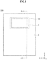
- FIG. 1 is a diagram depicting an example of a mirror with display device 100 according to an embodiment.
- FIG. 2 is a diagram depicting a cross-section cut along a line A-A in FIG. 1 .
- an X-direction is a direction of a width of the mirror with display device 100
- a Y-direction is a direction of a thickness of the mirror with display device 100
- a Z-direction is a direction of a height of the mirror with display device 100.
- the mirror with display device 100 includes, as illustrated in FIG. 1 , in a front view, a translucent part 1 and a mirror surface part 2.
- the mirror with display device 100 according to the embodiment includes, as illustrated in FIG. 2 , a transparent planar material 10 in which a metallic thin film 20 is provided on one surface, and a light-shielding part 40 is formed on the other surface so that the translucent part 1 is formed.
- a display part for displaying an image from the display device 30 is bonded at a position corresponding to the translucent part 1, via an adhesive layer 11.
- a mirror surface part 2 is constituted in the region where the metallic thin film 20 is arranged on one surface of the transparent planar material 10 and where the light-shielding part 40 is arranged on the other surface, and when the display device is in the ON time and in the OFF time.
- the translucent part 1 becomes a mirror surface.
- a surface of the transparent planar material 10 on which the display device is provided will be referred to as a back surface
- a surface of the transparent planar material 10 on which the metallic thin film 20 is arranged will be referred to as a front surface.
- the transparent planar material 10 is, for example, an inorganic glass such as a soda lime glass, an aluminosilicate glass, an aluminoborosilicate glass, or an alkali-free glass, or a transparent resin, such as a polycarbonate resin, or an acrylic resin.
- the transparent surface may be a laminated glass in which a plurality of glass plates are bonded via an intermediate film, or may be a laminated body in which a glass plate and a transparent resin are bonded via an intermediate film or transparent resins are bonded via an intermediate film.
- a publicly known material can be used for the intermediate film used in the laminated glass and the laminated body.
- the material includes PVB (polyvinyl butyral), EVA (ethylene vinyl acetate) or the like.
- the laminated glass may include three inorganic glass plates.
- the material may be subjected to a surface tempering treatment, such as a chemically tempering treatment or a physically tempering treatment.
- the transparent planar material 10 has a rectangular shape. But, the material may have any shape other than the rectangular shape. Moreover, a thickness of the transparent planar material 10 is, for example, 2 to 6mm.
- the transparent planar material 10 has a metallic thin film 20 and a light-shielding part 40, and enable forming of the light-shielding part 40 is arranged so as to form a translucent part 1.
- the metallic thin film 20 and the light-shielding part 40 may be arranged on the same surface of the transparent planar material 10, or may be arranged on different surfaces, respectively.
- the light-shielding part 40 is preferably formed between the metallic thin film 20 and the display device 30.
- a metallic thin film 20 is arranged on one surface of the transparent planar material 10.
- a visible light for light wavelengths falling within a range of 400 to 600 nm (The same applies to the following.)
- a mirror surface part 2 is formed on the transparent planar material 10.
- the metallic thin film 20 is preferably arranged on the front surface of the transparent planar material 10 (a surface that does not face the display part). According to the above-described configuration, the effect of reflecting a visible light becomes more prominent, and a design property of the mirror with display device is enhanced.
- the metallic thin film 20 is a film of a metal, a metallic oxide, or a metallic nitride.
- the metallic film may be configured by a single film or a plurality of films.
- the metallic thin film 20 may be formed directly on a surface of the transparent planar material 10, or may be formed by adhering a film having the metallic thin film 20 to the transparent planar material 10 via an adhesive layer. In this case, the adhesive layer is not limited.
- An average reflectance of the metallic thin film 20 for a visible light is, for example, 10 - 90%.
- the average reflectance is preferably greater than 50% and less than or equal to 90% for a case of making a reflected image clearer.
- the average reflectance is preferably 20 - 50% in the case of making image transmission of the display device 30 clearer. When the average reflectance falls within a range of 20 - 50%, a mirror that is excellent in image reproducibility can be obtained with the translucent part 1 for the display device being OFF and the mirror surface part 2.
- the average reflectance of the metallic thin film 20 for a visible light is preferably 25 to 45% and more preferably 30 to 40% in that a clear image can be displayed on the translucent part 1 when the display device 30 is ON, and a mirror that is excellent in image reproducibility can be obtained with the translucent part 1 for the display device 30 being OFF and the mirror surface part 2.
- the mirror excellent in image reproducibility indicates reproducibility not to the extent that an image is visible on the mirror surface, but to the extent that color and a shape of the image can be clearly recognized.
- the metallic thin film 20 preferably has a high average transmittance for a visible light, and is preferably a film that reflects an infrared light (for light wavelengths falling within a range of 800 nm - 2000 nm (The same applies to the following)).
- an infrared light for light wavelengths falling within a range of 800 nm - 2000 nm (The same applies to the following)
- the average transmittance of the metallic thin film 20 for a visible light is preferably 50% or more. When the average transmittance is 50% or more, a clear display image can be displayed on the translucent part 1 when the display device 30 is ON.
- the average transmittance is preferably 55% or more, and more preferably 60% or more, on the point of improving the clarity of an image.
- the average transmittance of the metallic thin film 20 for a visible light is preferably 80% or less.
- An average reflectance of the metallic thin film 20 for an infrared light is preferably 5% or more, and more preferably 10% or more. When the average reflectance for an infrared light is 5% or more, a heat damage of the display device 30 can be reduced.
- a deposition method for the metallic thin film 20 includes a sputtering method, a vapor deposition method, a wet coating method, or the like.
- An appropriate deposition method may be employed according to a material used for the metallic thin film 20. The above-described method is the same in the case of depositing directly on the transparent planar material 10 and in the case of depositing on another film.
- a metallic material for the metallic thin film 20 is preferably, Si, Sn, Zn, Al, Ti, In, or Cr.
- the metallic oxide is preferably an oxide of the above-described metal.
- the metallic nitride is preferably a nitride of the above-described metal.
- a typical material for the metallic thin film 20 includes ITO (Indium Tin Oxide), Al, or a cobalt oxide.
- a film thickness of the metallic thin film 20, as a whole, is preferably 50 - 500 nm, and more preferably 100 to 200 nm.
- a thickness of each metallic thin firm can be set freely, but the film thickness, as a whole, preferably falls within the above-described range.
- a resin thin film (not shown) may be arranged to an extent of not decreasing the above-described spectroscopic characteristics for the metallic thin film 20. Arranging the resin thin film is preferable, because antifouling performance or ease of cleanliness can be improved thereby.
- the resin thin film includes a fluorine resin, a silicon resin or the like. When the resin thin film layer of fluorine resin is arranged, the resin thin film can be formed by a vapor deposition method, and by adhering films configured by the above-described resin via an adhesive layer.
- the light-shielding part 40 is formed so as to have the translucent part 1.
- a region where the light-shielding part 40 is not formed constitutes the translucent part 1 as viewed from the front surface side of the transparent planar material 10.
- a region where the light-shielding part 40 constitutes formed is the mirror surface part 2 as viewed from the front surface side of the transparent planar material 10.
- the light-shielding part 40 is preferably arranged on the back surface of the transparent planar material 10 (surface facing the display part). According to the above-described configuration, a border between the light-shielding part 40 and the translucent part 1 becomes less prominent, and the design property is enhanced.
- a color of the light-shielding part 40 is preferably close to a color of the display surface when the display device 30 is OFF. According to the above-described configuration, the border between the translucent part 1 and the mirror surface part 2 becomes further indistinct when the display device 30 is OFF. As a result, a mirror can be obtained in which the translucent part 1 and the mirror surface part 2, of the mirror with display device 100, are integrated.
- the display surface is a color close to black, and the light-shielding part 40 is preferably black.
- the light-shielding part 40 preferably has an average transmittance of 1% or less for a visible light (wavelength of light is 400 - 600 nm), and more preferably 0% substantially.
- the average transmittance of the light-shielding part 40 is 1% or less, when viewed from the front surface side of the transparent planar material 10, the back surface cannot be seen, and the light-shielding part 40 functions as a mirror surface sufficiently.
- a shape of the translucent part 1 is not limited to a rectangular shape. The shape may be changed freely depending on a size of the display device, a display image of the display device, or the like.
- a method of forming the light-shielding part 40 includes, a method of forming directly on the transparent planar material 10, a method of forming by adhering a planar material having a light-shielding part to the transparent planar material 10, a method of adhering a resin film with the average transmittance for a visible light that falls within the above-described range, or the like.
- the method of forming directly on the transparent planar material 10 includes, for example, a screen printing using a paint including ceramic pigment, an inkjet printing, or the like.
- the forming method of adhering a planar material having a light-shielding part to the transparent planar material 10 includes a method of forming a light-shielding part on another planar material by the above-described method, and adhering the other planar material to the transparent planar material 10 via PVB (polyvinyl butyral) or the like.
- the method of adhering a resin film with an average transmittance for a visible light that falls within the above described range includes, for example, a method of adhering a black PET (polyethylene terephthalate) film to the transparent planar material 10 via an adhesive layer.
- a black PET polyethylene terephthalate
- the number of the translucent parts 1 of the transparent planar material 10, and a position, an area, and a shape for which a translucent part 1 is arranged are not limited. Therefore, the light-shielding part 40 of the mirror with display device 100 is formed to have a configuration according to a desired design with respect to the number of the translucent parts 1, the position, the area, the shape or the like.
- the display device 30 includes, for example, a liquid crystal display device, an organic EL display device, a plasma display device, or the like.
- the display device 30 displays, for example, an image stored in a storage device (not shown), or an image sent from a computer, a server, or the like connected via a network.
- a liquid crystal display device is used as the display device 30.
- a display panel 31 is bonded to the transparent planar material 10 via the adhesive layer 11.
- a back light 32 is arranged on the back surface side of the display panel 31.
- the display part for displaying an image of the display device 30 is bonded to the transparent planar material 10 via the adhesive layer 11, with respect to the back surface of the translucent part 1 of the transparent planar material 10, a display image displayed on the display device 30 is not readily reflected. As a result, when the display device 30 is ON, a distinct display image can be displayed on a front surface side of the transparent planar material 10.
- An area of the display part for displaying an image of the display device 30 is preferably greater than the area of the translucent part.
- outer peripheral edges of the display part are arranged so as to overlap with the light-shielding part 40.
- the display device 30 may include a chassis for protecting the display panel 31 and the back light 32.
- the chassis is preferably bonded to the light-shielding part 40 via another adhesive layer (not shown) different from the adhesive layer 11. According to the above-described configuration, even when the mirror with display device 100 is viewed from the front surface side of the transparent planar material 10, a bonded part between the chassis and the transparent planar material 10 is not identifiable, and the mirror with display device is excellent in design nature.
- the display part for displaying an image of the display device 30 is bonded to the translucent part 1 via the adhesive layer.
- the translucent part 1 becomes a mirror surface, and a border between the translucent part 1 and the mirror surface part 2 becomes indistinct.
- the mirror with display device 100 functions as an integrated mirror.
- the display device 30 is ON, on the back surface of the translucent part 1 of the transparent planar material 10, reflection of a display image is reduced.
- a sharp display image can be displayed on a front surface side of the transparent planar material 10.
- an intensity of a light of a display image passing through the translucent part 1 does not readily decrease, an intensity of a light of the display device 30 need not be high. Therefore, heat or power consumption due to a high intensity of light of the display device 30 can be reduced.
- the adhesive layer 11 preferably has a shear storage modulus G' within a range of 10 3 Pa to 10 7 Pa at 25 °C and at 1 Hz.
- the adhesive layer 11, the transparent planar material 10 and the display device 30 can be sufficiently wet with a shape of the adhesive layer 11 maintained; thus, the display device 30 and the transparent planar material 10 can be firmly fixed.
- the shear storage modulus G' of the adhesive layer 11 is more preferably 10 4 Pa to 10 6 Pa, and the shear storage modulus G' is further preferably 10 4 Pa to 10 5 Pa.
- a thickness of the adhesive layer 11 is, for example, preferably 0.03 mm to 2 mm, and more preferably 0.1 mm to 1 mm. If the thickness of the adhesive layer 11 is 0.03 mm or more, when an external force or the like is applied from the front surface side of the transparent planar material 10, the adhesive layer 11 reduces an impact of the external force, and thereby protects the display device 30. Moreover, even if a foreign matter with a size less than the thickness of the adhesive layer 11 enters between the display device 30 and the transparent planar material 10, because the thickness of the adhesive layer 11 does not change, any effect due to an entrance of a foreign matter on visibility can be controlled. Furthermore, from the standpoint of ensuring a visibility of a display part of the display device 30, the thickness of the adhesive layer 11 is preferably 2 mm or less.
- FIG. 3A and FIG. 3B are cross-sectional diagrams depicting examples in which a sheet of the inorganic glass or the transparent resin is used as the transparent planar material 10.
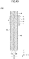
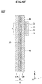
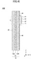
- FIGs. 4A to 4J are cross-sectional diagrams depicting examples in which a laminated glass or a laminated body is used as the transparent planar material 10.
- the mirror with display device according to the present invention can take forms as illustrated in the drawings.
- a mirror with display device 101A illustrated in FIG. 3A , includes a metallic thin film 20 and a light-shielding part 40 on a front surface of a transparent planar material 10.
- a light-shielding part 40 is formed between the metallic thin film 20 and a display device 30. Then, a back surface of the transparent planar material 10 is bonded to a display part of the display device 30 via an adhesive layer 11.
- a mirror with display device 101B illustrated in FIG. 3B , includes a metallic thin film 20 and a light-shielding part 40 on a back surface of a transparent planar material 10.
- a light-shielding part 40 is formed between the metallic thin film 20 and a display device 30. Then, a back surface of the transparent planar material 10 is bonded to a display part of the display device 30 via an adhesive layer 11.
- FIGs. 4A to FIG. 4J are diagrams depicting examples of a laminated glass formed by laminating a first glass plate and a second glass plate via an intermediate film of PVB (polyvinyl butyral).
- a glass plate of a front surface (surface that does not face the display part) of the transparent planar material 10 will be referred to as a first glass plate 10A
- a glass plate of a back surface (surface that faces the display part) of the transparent planar material 10 will be referred to as a second glass plate 10B.
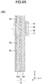
- the mirror with display device 102A illustrated in FIG. 4A , includes a metallic thin film 20 and a light-shielding part 40 on a surface, of the first glass plate 10A of the transparent planar material 10, that does not contact the intermediate film 13.
- the light-shielding part 40 is formed between the metallic thin film 20 and the display device 30.
- the second glass plate 10B of the transparent planar material 10 is bonded to a display part of the display device 30 via the adhesive layer 11.
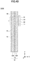
- the mirror with display device 102B illustrated in FIG. 4B , includes a metallic thin film 20 on a surface, of the first glass plate 10A of the transparent planar material 10, that does not contact the intermediate film 13, and includes a light-shielding part 40 on a surface that contacts the intermediate film 13. Then, the second glass plate 10B of the transparent planar material 10 is bonded to a display part of the display device 30 via the adhesive layer 11.
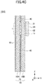
- the mirror with display device 102C illustrated in FIG. 4C , includes a metallic thin film 20 on a surface, of the first glass plate 10A of the transparent planar material 10, that does not contact the intermediate film 13.
- a light-shielding part 40 on a surface, of the second glass plate 10B of the transparent planar material 10, that contacts the intermediate film 13 is included; the surface which does not contact the intermediate film 13 is bonded to a display part of the display device 30 via the adhesive layer 11.
- the mirror with display device 102D illustrated in FIG. 4D , includes a metallic thin film 20 on a surface, of the first glass plate 10A of the transparent planar material 10, that does not contact the intermediate film 13, and includes a light-shielding part 40 on a surface of the second glass plate 10B of the transparent planar material 10 that does not contact the intermediate film 13.
- the same surface is bonded to a display part of the display device 30 via the adhesive layer 11.
- the mirror with display device 102E illustrated in FIG. 4E , includes a metallic thin film 20 and a light-shielding part 40 on a surface, of the first glass plate 10A of the transparent planar material 10, that contacts the intermediate film 13.
- the light-shielding part 40 is formed between the metallic thin film 20 and the display device 30.
- the second glass plate 10B of the transparent planar material 10 is bonded to a display part of the display device 30 via the adhesive layer 11.
- the mirror with display device 102F illustrated in FIG. 4F , includes a metallic thin film 20 on a surface, of the first glass plate 10A of the transparent planar material 10, that contacts the intermediate film 13, and includes a light-shielding part 40 on a surface of the second glass plate 10B that contacts the intermediate film 13.
- the surface that does not contact the intermediate film 13 is bonded to a display part of the display device 30 via the adhesive layer 11.
- the mirror with display device 102G illustrated in FIG. 4G , includes a metallic thin film 20 on a surface, of the first glass plate 10A of the transparent planar material 10, that contacts the intermediate film 13, and includes a light-shielding part 40 on a surface of the second glass plate 10B that does not contact the intermediate film 13. The same surface is bonded to a display part of the display device 30 via the adhesive layer 11.
- the mirror with display device 102H illustrated in FIG. 4H , includes a metallic thin film 20 and a light-shielding part 40 on a surface, of the second glass plate 10B of the transparent planar material 10, that contacts the intermediate film 13.
- the light-shielding part 40 is formed between the metallic thin film 20 and the display device 30. Then, a surface of the second glass plate 10B that does not contact the intermediate film 13 is bonded to a display part of the display device 30 via the adhesive layer 11.
- the mirror with display device 102I illustrated in FIG. 4I , includes a metallic thin film 20 on a surface, of the second glass plate 10B of the transparent planar material 10, that contacts the intermediate film 13, and includes a light-shielding part 40 on a surface that does not contact the intermediate film 13. Then, a surface of the second glass plate 10B that does not contact the intermediate film 13 is bonded to a display part of the display device 30 via the adhesive layer 11.
- the mirror with display device 102J illustrated in FIG. 4J , includes a metallic thin film 20 and a light-shielding part 40 on a surface, of the second glass plate 10B of the transparent planar material 10, that does not contact the intermediate film 13.
- the light-shielding part 40 is formed between the metallic thin film 20 and the display device 30. Then, a surface of the second glass plate 10B that does not contact the intermediate film 13 is bonded to a display part of the display device 30 via the adhesive layer 11.
- the mirror with display device according to the embodiment has been described.
- the present invention is not limited to the embodiments, and various variations and modifications may be made without deviating from the scope of the present invention.
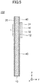
- FIG. 5 is a cross-sectional diagram schematically depicting a conventional mirror with display device 200.
- the conventional mirror with display device 200 includes a metallic thin film 20 on one surface, and a transparent planar material 10 on which a light-shielding part 40 is formed on another surface such that arrangement of a translucent part 1 can be enabled.
- a display device 30 is arranged so as to face the translucent part 1.
- an air layer 12 is formed between a back surface side of the translucent part 1 and a display device 30.
- a border between the translucent part 1 and a mirror surface part 2 becomes distinct.
- the border between the translucent part 1 and the mirror surface part 2 becomes distinct, and a design property is low.
- the display device is ON, multiple reflections occur on a back surface of the translucent part 1 and a front surface of the display device 30.
- a display image viewed from the front surface side of the transparent planar material 10 becomes indistinct.
- a light intensity of the display device 30 is required to be increased.
- the mirror with display device 100 can be arranged, for example, on a partition wall, a column support, or the like of a shop.
- a customer can use the mirror with display device for acquiring information about products, floor guide, or the like, which is displayed on the display device 30.
- the mirror with display device is arranged in a clothing shop, the appearance customer wearing various products with different colors and designs can be displayed in a virtual manner on the display device 30, such that the customer can examine his or her appearance for various products.
- the mirror with display device is arranged in a fitting room of a clothing shop, a back shot of the customer who tries on a product is shot by a camera, and is displayed on the display device 30, such that the customer can examine the back shot when trying on a product.
- a use of the mirror with display device 100 is not limited to the above-described examples.
- the mirror with display device 100 of the embodiment by bonding the display device 30 to a back surface of the translucent part 1 of the transparent planar material 10 via the adhesive layer 11, visibility of an image displayed on the display device 30 is enhanced.
Landscapes
- Physics & Mathematics (AREA)
- General Physics & Mathematics (AREA)
- Nonlinear Science (AREA)
- Optics & Photonics (AREA)
- Chemical & Material Sciences (AREA)
- Crystallography & Structural Chemistry (AREA)
- Engineering & Computer Science (AREA)
- Theoretical Computer Science (AREA)
- Mathematical Physics (AREA)
- Devices For Indicating Variable Information By Combining Individual Elements (AREA)
- Optical Elements Other Than Lenses (AREA)
Abstract
Description
- The disclosure herein generally relates to a mirror with display device, in which the display device is adhered directly to a surface of the mirror.
- As an example of configuring a mirror and a display device as a unit, a configuration has been known in which a translucent part is formed in a part of the mirror, and the display device is arranged on a back side of the translucent part so that a user see a display surface of the display device while seeing the mirror (See
Patent Documents 1 and 2). -
Patent Document 1 discloses a thin display apparatus in which a half mirror is arranged on a front surface side of a thin display device. The half mirror disclosed inPatent Document 1 is provided with display device on a back surface of a glass plate. The half mirror includes a translucent region in which the display device is present, and a light-shielding layer formed in a region which does not have the display device. In the configuration described inPatent Document 1, a metallic thin film layer is arranged on a surface of the glass plate where the display device is present. A transparent film is arranged between the metallic thin film layer and the light-shielding layer. Therefore, intensity of a light passing through the translucent region is small. -
Patent Document 2 discloses a mirror for vehicle with display device. In the mirror for vehicle, on an entire front surface of a glass plate, a light transmissive metallic thin film layer for a half mirror is formed. In a part of a back surface of the glass plate, a black paint film is formed so as to form a light transmission window. Furthermore, a liquid crystal display device is arranged at a position facing the light transmission window. -
- [PTL 1] Japanese Unexamined Patent Application Publication No.
2011-71973 - [PTL 2] Japanese Unexamined Patent Application Publication No.
2002-67806 - In the related art, in a state where the display device is not caused to operate (OFF time), the light-shielding part cannot be made sufficiently black, and a border between the translucent part and the light-shielding part has been visible. Moreover, in the related art, in a state where the display device is caused to operate (ON time), there is a problem that when viewing an image through a transparent planar material (glass plate), due to multiple reflections, a display image becomes indistinct. In order to display a sharp image, the intensity of light of the display device needs to be strong so as to make an intensity of a reflected image relatively smaller.
- The present invention was made in view of such a problem, and it is an object of the present invention to provide a mirror with display device, in which in an OFF time of the display apparatus a border between a light-shielding part and a translucent part is not visible, and in an ON time of the display apparatus a sharp image is displayed in a translucent part.
- According to study by inventors of the present invention, the inventors have found that when the display part of the display device for displaying an image and a transparent planar material are bonded via an adhesive layer, multiple reflections on the surfaces of the display device and the transparent planar material are reduced, and that the above-described problem can be solved, and thereby completed the present invention.
- That is, a mirror with display device according to the present invention includes a transparent planar material; and a display device. The transparent planar material has a metallic thin film. A light-shielding part is formed in the transparent planar material so that the transparent planar material has a translucent part. A display part of the display device for displaying an image is bonded to the translucent part via an adhesive layer.
- According to the mirror with display device of the present invention, in an OFF time of the display device, a border between the light-shielding part and the translucent part is not visible, and in an ON time of the display device, a sharp image can be displayed on the translucent part.
- Other objects and further features of embodiments will become apparent from the following detailed description when read in conjunction with the accompanying drawings, in which:
- [
FIGURE 1 ]
FIG. 1 is a front view depicting a mirror with display device according to an embodiment of the present invention. - [
FIGURE 2 ]
FIG. 2 is a diagram schematically depicting a cross-section cut along a line A-A inFIG. 1 . - [
FIGURE 3A ]
FIG. 3A is a cross-sectional diagram depicting an example of a mirror with display device in which a transparent planar material is a single plate. - [
FIGURE 3B ]
FIG. 3B is a cross-sectional diagram depicting another example of the mirror with display device in which the transparent planar material is a single plate. - [
FIGURE 4A ]
FIG. 4A is a cross-sectional diagram depicting an example of a mirror with display device in which a transparent planar material is a laminated body. - [
FIGURE 4B ]
FIG. 4B is a cross-sectional diagram depicting another example of the mirror with display device in which the transparent planar material is a laminated body. - [
FIGURE 4C ]
FIG. 4C is a cross-sectional diagram depicting still another example of the mirror with display device in which the transparent planar material is a laminated body. - [
FIGURE 4D ]
FIG. 4D is a cross-sectional diagram depicting yet another example of the mirror with display device in which the transparent planar material is a laminated body. - [
FIGURE 4E ]
FIG. 4E is a cross-sectional diagram depicting still another example of the mirror with display device in which the transparent planar material is a laminated body. - [
FIGURE 4F ]
FIG. 4F is a cross-sectional diagram depicting yet another example of the mirror with display device in which the transparent planar material is a laminated body. - [
FIGURE 4G ]
FIG. 4G is a cross-sectional diagram depicting still another example of the mirror with display device in which the transparent planar material is a laminated body. - [
FIGURE 4H ]
FIG. 4H is a cross-sectional diagram depicting yet another example of the mirror with display device in which the transparent planar material is a laminated body. - [
FIGURE 4I ]
FIG. 4I is a cross-sectional diagram depicting still another example of the mirror with display device in which the transparent planar material is a laminated body. - [
FIGURE 4J ]
FIG. 4J is a cross-sectional diagram depicting yet another example of the mirror with display device in which the transparent planar material is a laminated body. - [
FIGURE 5 ]
FIG. 5 is a diagram schematically depicting a cross-section of a conventional mirror with display device. - In the following, with reference to drawings, embodiments of the present invention will be described. In each drawing, the same reference numeral is assigned to the same component, and redundant explanation will be omitted.
-
FIG. 1 is a diagram depicting an example of a mirror withdisplay device 100 according to an embodiment. Moreover,FIG. 2 is a diagram depicting a cross-section cut along a line A-A inFIG. 1 . InFIG. 1 andFIG. 2 , an X-direction is a direction of a width of the mirror withdisplay device 100, a Y-direction is a direction of a thickness of the mirror withdisplay device 100, and a Z-direction is a direction of a height of the mirror withdisplay device 100. - The mirror with
display device 100 according to the embodiment includes, as illustrated inFIG. 1 , in a front view, atranslucent part 1 and amirror surface part 2. The mirror withdisplay device 100 according to the embodiment includes, as illustrated inFIG. 2 , a transparentplanar material 10 in which a metallicthin film 20 is provided on one surface, and a light-shieldingpart 40 is formed on the other surface so that thetranslucent part 1 is formed. On the other surface of the transparentplanar material 10, a display part for displaying an image from thedisplay device 30 is bonded at a position corresponding to thetranslucent part 1, via anadhesive layer 11. - For the mirror with
display device 100 according to the embodiment, amirror surface part 2 is constituted in the region where the metallicthin film 20 is arranged on one surface of the transparentplanar material 10 and where the light-shieldingpart 40 is arranged on the other surface, and when the display device is in the ON time and in the OFF time. In the mirror withdisplay device 100 according to the embodiment, when thedisplay device 30 is in the ON time, a display image is displayed in thetranslucent part 1, and when thedisplay device 30 is in the OFF time, thetranslucent part 1 becomes a mirror surface. As a result, when the display device is in the OFF time, the border between thetranslucent part 1 and themirror surface part 2 is not visible, and an integrated mirror can be obtained. - In the following description, a surface of the transparent
planar material 10 on which the display device is provided will be referred to as a back surface, and a surface of the transparentplanar material 10 on which the metallicthin film 20 is arranged will be referred to as a front surface. - The transparent
planar material 10 is, for example, an inorganic glass such as a soda lime glass, an aluminosilicate glass, an aluminoborosilicate glass, or an alkali-free glass, or a transparent resin, such as a polycarbonate resin, or an acrylic resin. Moreover, the transparent surface may be a laminated glass in which a plurality of glass plates are bonded via an intermediate film, or may be a laminated body in which a glass plate and a transparent resin are bonded via an intermediate film or transparent resins are bonded via an intermediate film. For the intermediate film used in the laminated glass and the laminated body, a publicly known material can be used. For example, the material includes PVB (polyvinyl butyral), EVA (ethylene vinyl acetate) or the like. - A number of the inorganic glasses and transparent resins configuring the laminated glass and the laminated body is not limited. For example, the laminated glass may include three inorganic glass plates.
- When the transparent
planar material 10 is inorganic glass, the material may be subjected to a surface tempering treatment, such as a chemically tempering treatment or a physically tempering treatment. - The transparent
planar material 10 according to the embodiment has a rectangular shape. But, the material may have any shape other than the rectangular shape. Moreover, a thickness of the transparentplanar material 10 is, for example, 2 to 6mm. - The transparent
planar material 10 has a metallicthin film 20 and a light-shieldingpart 40, and enable forming of the light-shieldingpart 40 is arranged so as to form atranslucent part 1. The metallicthin film 20 and the light-shieldingpart 40 may be arranged on the same surface of the transparentplanar material 10, or may be arranged on different surfaces, respectively. In order to reduce the visibility of the border between thetranslucent part 1 and themirror surface part 2, the light-shieldingpart 40 is preferably formed between the metallicthin film 20 and thedisplay device 30. - On one surface of the transparent
planar material 10, a metallicthin film 20 is arranged. By arranging the metallicthin film 20 on one surface of the transparentplanar material 10, a visible light (for light wavelengths falling within a range of 400 to 600 nm (The same applies to the following.)) is more reflected than in a case of using the transparentplanar material 10 alone. Then, when a light-shieldingpart 40 is arranged on the back surface of the transparentplanar material 10, amirror surface part 2 is formed on the transparentplanar material 10. - The metallic
thin film 20 is preferably arranged on the front surface of the transparent planar material 10 (a surface that does not face the display part). According to the above-described configuration, the effect of reflecting a visible light becomes more prominent, and a design property of the mirror with display device is enhanced. - The metallic
thin film 20 is a film of a metal, a metallic oxide, or a metallic nitride. The metallic film may be configured by a single film or a plurality of films. The metallicthin film 20 may be formed directly on a surface of the transparentplanar material 10, or may be formed by adhering a film having the metallicthin film 20 to the transparentplanar material 10 via an adhesive layer. In this case, the adhesive layer is not limited. - An average reflectance of the metallic
thin film 20 for a visible light is, for example, 10 - 90%. The average reflectance is preferably greater than 50% and less than or equal to 90% for a case of making a reflected image clearer. The average reflectance is preferably 20 - 50% in the case of making image transmission of thedisplay device 30 clearer. When the average reflectance falls within a range of 20 - 50%, a mirror that is excellent in image reproducibility can be obtained with thetranslucent part 1 for the display device being OFF and themirror surface part 2. The average reflectance of the metallicthin film 20 for a visible light is preferably 25 to 45% and more preferably 30 to 40% in that a clear image can be displayed on thetranslucent part 1 when thedisplay device 30 is ON, and a mirror that is excellent in image reproducibility can be obtained with thetranslucent part 1 for thedisplay device 30 being OFF and themirror surface part 2. The mirror excellent in image reproducibility indicates reproducibility not to the extent that an image is visible on the mirror surface, but to the extent that color and a shape of the image can be clearly recognized. - The metallic
thin film 20 preferably has a high average transmittance for a visible light, and is preferably a film that reflects an infrared light (for light wavelengths falling within a range of 800 nm - 2000 nm (The same applies to the following)). By making the average transmittance for a visible light high, it is possible to transmit sufficiently a light emitted from thedisplay device 30 bonded to a back surface (surface facing the display part) via theadhesive layer 11, and to display a clear image. Moreover, by enhancing the reflectance for an infrared light, external heat is not transferred from the transparentplanar material 10 to the inside, and a heat damage of thedisplay device 30 can be reduced. - The average transmittance of the metallic
thin film 20 for a visible light is preferably 50% or more. When the average transmittance is 50% or more, a clear display image can be displayed on thetranslucent part 1 when thedisplay device 30 is ON. The average transmittance is preferably 55% or more, and more preferably 60% or more, on the point of improving the clarity of an image. In order to obtain a mirror that is excellent in image reproducibility with thetranslucent part 1 for thedisplay device 30 being OFF and themirror surface part 2, the average transmittance of the metallicthin film 20 for a visible light is preferably 80% or less. - An average reflectance of the metallic
thin film 20 for an infrared light is preferably 5% or more, and more preferably 10% or more. When the average reflectance for an infrared light is 5% or more, a heat damage of thedisplay device 30 can be reduced. - A deposition method for the metallic
thin film 20 includes a sputtering method, a vapor deposition method, a wet coating method, or the like. An appropriate deposition method may be employed according to a material used for the metallicthin film 20. The above-described method is the same in the case of depositing directly on the transparentplanar material 10 and in the case of depositing on another film. - A metallic material for the metallic
thin film 20 is preferably, Si, Sn, Zn, Al, Ti, In, or Cr. The metallic oxide is preferably an oxide of the above-described metal. The metallic nitride is preferably a nitride of the above-described metal. A typical material for the metallicthin film 20 includes ITO (Indium Tin Oxide), Al, or a cobalt oxide. - A film thickness of the metallic
thin film 20, as a whole, is preferably 50 - 500 nm, and more preferably 100 to 200 nm. When the metallic thin film is configured by a plurality of metallic thin films, a thickness of each metallic thin firm can be set freely, but the film thickness, as a whole, preferably falls within the above-described range. - On the surface of the metallic thin film 20 (on the surface at which the transparent
planar material 10 is not provided), a resin thin film (not shown) may be arranged to an extent of not decreasing the above-described spectroscopic characteristics for the metallicthin film 20. Arranging the resin thin film is preferable, because antifouling performance or ease of cleanliness can be improved thereby. The resin thin film includes a fluorine resin, a silicon resin or the like. When the resin thin film layer of fluorine resin is arranged, the resin thin film can be formed by a vapor deposition method, and by adhering films configured by the above-described resin via an adhesive layer. - On one surface of the transparent
planar material 10, the light-shieldingpart 40 is formed so as to have thetranslucent part 1. A region where the light-shieldingpart 40 is not formed constitutes thetranslucent part 1 as viewed from the front surface side of the transparentplanar material 10. A region where the light-shieldingpart 40 constitutes formed is themirror surface part 2 as viewed from the front surface side of the transparentplanar material 10. - The light-shielding
part 40 is preferably arranged on the back surface of the transparent planar material 10 (surface facing the display part). According to the above-described configuration, a border between the light-shieldingpart 40 and thetranslucent part 1 becomes less prominent, and the design property is enhanced. - A color of the light-shielding
part 40 is preferably close to a color of the display surface when thedisplay device 30 is OFF. According to the above-described configuration, the border between thetranslucent part 1 and themirror surface part 2 becomes further indistinct when thedisplay device 30 is OFF. As a result, a mirror can be obtained in which thetranslucent part 1 and themirror surface part 2, of the mirror withdisplay device 100, are integrated. - When the
display device 30 is a liquid crystal display device, the display surface is a color close to black, and the light-shieldingpart 40 is preferably black. - The light-shielding
part 40 preferably has an average transmittance of 1% or less for a visible light (wavelength of light is 400 - 600 nm), and more preferably 0% substantially. When the average transmittance of the light-shieldingpart 40 is 1% or less, when viewed from the front surface side of the transparentplanar material 10, the back surface cannot be seen, and the light-shieldingpart 40 functions as a mirror surface sufficiently. - A shape of the
translucent part 1 is not limited to a rectangular shape. The shape may be changed freely depending on a size of the display device, a display image of the display device, or the like. - A method of forming the light-shielding
part 40 includes, a method of forming directly on the transparentplanar material 10, a method of forming by adhering a planar material having a light-shielding part to the transparentplanar material 10, a method of adhering a resin film with the average transmittance for a visible light that falls within the above-described range, or the like. - The method of forming directly on the transparent
planar material 10 includes, for example, a screen printing using a paint including ceramic pigment, an inkjet printing, or the like. - The forming method of adhering a planar material having a light-shielding part to the transparent
planar material 10 includes a method of forming a light-shielding part on another planar material by the above-described method, and adhering the other planar material to the transparentplanar material 10 via PVB (polyvinyl butyral) or the like. - The method of adhering a resin film with an average transmittance for a visible light that falls within the above described range includes, for example, a method of adhering a black PET (polyethylene terephthalate) film to the transparent
planar material 10 via an adhesive layer. - The number of the
translucent parts 1 of the transparentplanar material 10, and a position, an area, and a shape for which atranslucent part 1 is arranged are not limited. Therefore, the light-shieldingpart 40 of the mirror withdisplay device 100 is formed to have a configuration according to a desired design with respect to the number of thetranslucent parts 1, the position, the area, the shape or the like. - To the back surface of the transparent
planar material 10 at the position corresponding to thetranslucent part 1, a display part for displaying an image of thedisplay device 30 is bonded via theadhesive layer 11. Thedisplay device 30 includes, for example, a liquid crystal display device, an organic EL display device, a plasma display device, or the like. Thedisplay device 30 displays, for example, an image stored in a storage device (not shown), or an image sent from a computer, a server, or the like connected via a network. - In the mirror with
display device 100 according to the embodiment, a liquid crystal display device is used as thedisplay device 30. In the liquid crystal display device, adisplay panel 31 is bonded to the transparentplanar material 10 via theadhesive layer 11. Furthermore, aback light 32 is arranged on the back surface side of thedisplay panel 31. - Because in the mirror with
display device 100 according to the embodiment, the display part for displaying an image of thedisplay device 30 is bonded to the transparentplanar material 10 via theadhesive layer 11, with respect to the back surface of thetranslucent part 1 of the transparentplanar material 10, a display image displayed on thedisplay device 30 is not readily reflected. As a result, when thedisplay device 30 is ON, a distinct display image can be displayed on a front surface side of the transparentplanar material 10. - An area of the display part for displaying an image of the
display device 30 is preferably greater than the area of the translucent part. In this case, outer peripheral edges of the display part are arranged so as to overlap with the light-shieldingpart 40. With the above-described configuration, the outer peripheral edges of the display part become invisible from a front surface of the transparentplanar material 10, and thereby an effect that an image displayed on thetranslucent part 1 appears floating toward the front surface side of the transparentplanar material 10 can be obtained. - The
display device 30 may include a chassis for protecting thedisplay panel 31 and theback light 32. The chassis is preferably bonded to the light-shieldingpart 40 via another adhesive layer (not shown) different from theadhesive layer 11. According to the above-described configuration, even when the mirror withdisplay device 100 is viewed from the front surface side of the transparentplanar material 10, a bonded part between the chassis and the transparentplanar material 10 is not identifiable, and the mirror with display device is excellent in design nature. - In the mirror with
display device 100 according to the embodiment, the display part for displaying an image of thedisplay device 30 is bonded to thetranslucent part 1 via the adhesive layer. According to the above-described configuration, in the mirror withdisplay device 100, when thedisplay device 30 is OFF, thetranslucent part 1 becomes a mirror surface, and a border between thetranslucent part 1 and themirror surface part 2 becomes indistinct. As a result, when thedisplay device 30 is OFF, the mirror withdisplay device 100 functions as an integrated mirror. Furthermore, when thedisplay device 30 is ON, on the back surface of thetranslucent part 1 of the transparentplanar material 10, reflection of a display image is reduced. As a result, when thedisplay device 30 is ON, a sharp display image can be displayed on a front surface side of the transparentplanar material 10. Furthermore, because an intensity of a light of a display image passing through thetranslucent part 1 does not readily decrease, an intensity of a light of thedisplay device 30 need not be high. Therefore, heat or power consumption due to a high intensity of light of thedisplay device 30 can be reduced. - The
adhesive layer 11 preferably has a shear storage modulus G' within a range of 103 Pa to 107 Pa at 25 °C and at 1 Hz. When the storage shear elasticity G' falls within the above-described range, theadhesive layer 11, the transparentplanar material 10 and thedisplay device 30 can be sufficiently wet with a shape of theadhesive layer 11 maintained; thus, thedisplay device 30 and the transparentplanar material 10 can be firmly fixed. The shear storage modulus G' of theadhesive layer 11 is more preferably 104 Pa to 106 Pa, and the shear storage modulus G' is further preferably 104 Pa to 105 Pa. - A thickness of the
adhesive layer 11 is, for example, preferably 0.03 mm to 2 mm, and more preferably 0.1 mm to 1 mm. If the thickness of theadhesive layer 11 is 0.03 mm or more, when an external force or the like is applied from the front surface side of the transparentplanar material 10, theadhesive layer 11 reduces an impact of the external force, and thereby protects thedisplay device 30. Moreover, even if a foreign matter with a size less than the thickness of theadhesive layer 11 enters between thedisplay device 30 and the transparentplanar material 10, because the thickness of theadhesive layer 11 does not change, any effect due to an entrance of a foreign matter on visibility can be controlled. Furthermore, from the standpoint of ensuring a visibility of a display part of thedisplay device 30, the thickness of theadhesive layer 11 is preferably 2 mm or less. -
FIG. 3A andFIG. 3B are cross-sectional diagrams depicting examples in which a sheet of the inorganic glass or the transparent resin is used as the transparentplanar material 10.FIGs. 4A to 4J are cross-sectional diagrams depicting examples in which a laminated glass or a laminated body is used as the transparentplanar material 10. The mirror with display device according to the present invention can take forms as illustrated in the drawings. - A mirror with
display device 101A, illustrated inFIG. 3A , includes a metallicthin film 20 and a light-shieldingpart 40 on a front surface of a transparentplanar material 10. A light-shieldingpart 40 is formed between the metallicthin film 20 and adisplay device 30. Then, a back surface of the transparentplanar material 10 is bonded to a display part of thedisplay device 30 via anadhesive layer 11. - A mirror with
display device 101B, illustrated inFIG. 3B , includes a metallicthin film 20 and a light-shieldingpart 40 on a back surface of a transparentplanar material 10. A light-shieldingpart 40 is formed between the metallicthin film 20 and adisplay device 30. Then, a back surface of the transparentplanar material 10 is bonded to a display part of thedisplay device 30 via anadhesive layer 11. -
FIGs. 4A to FIG. 4J are diagrams depicting examples of a laminated glass formed by laminating a first glass plate and a second glass plate via an intermediate film of PVB (polyvinyl butyral). In the following description, a glass plate of a front surface (surface that does not face the display part) of the transparentplanar material 10 will be referred to as afirst glass plate 10A, and a glass plate of a back surface (surface that faces the display part) of the transparentplanar material 10 will be referred to as asecond glass plate 10B. - The mirror with
display device 102A, illustrated inFIG. 4A , includes a metallicthin film 20 and a light-shieldingpart 40 on a surface, of thefirst glass plate 10A of the transparentplanar material 10, that does not contact theintermediate film 13. The light-shieldingpart 40 is formed between the metallicthin film 20 and thedisplay device 30. Then, thesecond glass plate 10B of the transparentplanar material 10 is bonded to a display part of thedisplay device 30 via theadhesive layer 11. - The mirror with
display device 102B, illustrated inFIG. 4B , includes a metallicthin film 20 on a surface, of thefirst glass plate 10A of the transparentplanar material 10, that does not contact theintermediate film 13, and includes a light-shieldingpart 40 on a surface that contacts theintermediate film 13. Then, thesecond glass plate 10B of the transparentplanar material 10 is bonded to a display part of thedisplay device 30 via theadhesive layer 11. - The mirror with
display device 102C, illustrated inFIG. 4C , includes a metallicthin film 20 on a surface, of thefirst glass plate 10A of the transparentplanar material 10, that does not contact theintermediate film 13. A light-shieldingpart 40 on a surface, of thesecond glass plate 10B of the transparentplanar material 10, that contacts theintermediate film 13 is included; the surface which does not contact theintermediate film 13 is bonded to a display part of thedisplay device 30 via theadhesive layer 11. - The mirror with
display device 102D, illustrated inFIG. 4D , includes a metallicthin film 20 on a surface, of thefirst glass plate 10A of the transparentplanar material 10, that does not contact theintermediate film 13, and includes a light-shieldingpart 40 on a surface of thesecond glass plate 10B of the transparentplanar material 10 that does not contact theintermediate film 13. The same surface is bonded to a display part of thedisplay device 30 via theadhesive layer 11. - The mirror with
display device 102E, illustrated inFIG. 4E , includes a metallicthin film 20 and a light-shieldingpart 40 on a surface, of thefirst glass plate 10A of the transparentplanar material 10, that contacts theintermediate film 13. The light-shieldingpart 40 is formed between the metallicthin film 20 and thedisplay device 30. Then, thesecond glass plate 10B of the transparentplanar material 10 is bonded to a display part of thedisplay device 30 via theadhesive layer 11. - The mirror with
display device 102F, illustrated inFIG. 4F , includes a metallicthin film 20 on a surface, of thefirst glass plate 10A of the transparentplanar material 10, that contacts theintermediate film 13, and includes a light-shieldingpart 40 on a surface of thesecond glass plate 10B that contacts theintermediate film 13. The surface that does not contact theintermediate film 13 is bonded to a display part of thedisplay device 30 via theadhesive layer 11. - The mirror with
display device 102G, illustrated inFIG. 4G , includes a metallicthin film 20 on a surface, of thefirst glass plate 10A of the transparentplanar material 10, that contacts theintermediate film 13, and includes a light-shieldingpart 40 on a surface of thesecond glass plate 10B that does not contact theintermediate film 13. The same surface is bonded to a display part of thedisplay device 30 via theadhesive layer 11. - The mirror with
display device 102H, illustrated inFIG. 4H , includes a metallicthin film 20 and a light-shieldingpart 40 on a surface, of thesecond glass plate 10B of the transparentplanar material 10, that contacts theintermediate film 13. The light-shieldingpart 40 is formed between the metallicthin film 20 and thedisplay device 30. Then, a surface of thesecond glass plate 10B that does not contact theintermediate film 13 is bonded to a display part of thedisplay device 30 via theadhesive layer 11. - The mirror with display device 102I, illustrated in
FIG. 4I , includes a metallicthin film 20 on a surface, of thesecond glass plate 10B of the transparentplanar material 10, that contacts theintermediate film 13, and includes a light-shieldingpart 40 on a surface that does not contact theintermediate film 13. Then, a surface of thesecond glass plate 10B that does not contact theintermediate film 13 is bonded to a display part of thedisplay device 30 via theadhesive layer 11. - The mirror with
display device 102J, illustrated inFIG. 4J , includes a metallicthin film 20 and a light-shieldingpart 40 on a surface, of thesecond glass plate 10B of the transparentplanar material 10, that does not contact theintermediate film 13. The light-shieldingpart 40 is formed between the metallicthin film 20 and thedisplay device 30. Then, a surface of thesecond glass plate 10B that does not contact theintermediate film 13 is bonded to a display part of thedisplay device 30 via theadhesive layer 11. - As described above, the mirror with display device according to the embodiment has been described. However, the present invention is not limited to the embodiments, and various variations and modifications may be made without deviating from the scope of the present invention.
-
FIG. 5 is a cross-sectional diagram schematically depicting a conventional mirror withdisplay device 200. As illustrated inFIG. 5 , the conventional mirror withdisplay device 200 includes a metallicthin film 20 on one surface, and a transparentplanar material 10 on which a light-shieldingpart 40 is formed on another surface such that arrangement of atranslucent part 1 can be enabled. On the other surface of the transparentplanar material 10, adisplay device 30 is arranged so as to face thetranslucent part 1. - Because in the mirror with display device 200 a peripheral part of a chassis of the
display device 30 is bonded to the light-shieldingpart 40 via an adhesive layer which is not shown, anair layer 12 is formed between a back surface side of thetranslucent part 1 and adisplay device 30. In the above-described configuration, when thedisplay device 30 is OFF, a border between thetranslucent part 1 and amirror surface part 2 becomes distinct. As a result, in the mirror withdisplay device 200, when thedisplay device 30 is OFF, the border between thetranslucent part 1 and themirror surface part 2 becomes distinct, and a design property is low. Furthermore, in the above-described configuration, when the display device is ON, multiple reflections occur on a back surface of thetranslucent part 1 and a front surface of thedisplay device 30. As a result, in the mirror withdisplay device 200, when thedisplay device 30 is ON, a display image viewed from the front surface side of the transparentplanar material 10 becomes indistinct. Moreover, in order to increase a light intensity of the display image, a light intensity of thedisplay device 30 is required to be increased. - The mirror with
display device 100 according to the embodiment can be arranged, for example, on a partition wall, a column support, or the like of a shop. A customer can use the mirror with display device for acquiring information about products, floor guide, or the like, which is displayed on thedisplay device 30. Furthermore, when the mirror with display device is arranged in a clothing shop, the appearance customer wearing various products with different colors and designs can be displayed in a virtual manner on thedisplay device 30, such that the customer can examine his or her appearance for various products. Moreover, when the mirror with display device is arranged in a fitting room of a clothing shop, a back shot of the customer who tries on a product is shot by a camera, and is displayed on thedisplay device 30, such that the customer can examine the back shot when trying on a product. A use of the mirror withdisplay device 100 is not limited to the above-described examples. - As described above, according to the mirror with
display device 100 of the embodiment, by bonding thedisplay device 30 to a back surface of thetranslucent part 1 of the transparentplanar material 10 via theadhesive layer 11, visibility of an image displayed on thedisplay device 30 is enhanced. - The present application is based on and claims the benefit of priority of Japanese Priority Application No.
2015-087075 filed on April 21, 2015 -
- 1
- translucent part
- 2
- mirror surface part
- 10
- transparent planar material
- 11
- adhesive layer
- 12
- air layer
- 20
- metallic thin film
- 30
- display device
- 31
- display panel
- 32
- back light
- 100
- mirror with display device
Claims (8)
- A mirror with display device comprising:a transparent planar material; anda display device,wherein the transparent planar material has a metallic thin film, and a light-shielding part is formed in the transparent planar material so that the transparent planar material has a translucent part, andwherein a display part of the display device for displaying an image is bonded to the translucent part via an adhesive layer.
- The mirror with display device according to claim 1,
wherein the light-shielding part is formed between the metallic thin film and the display device. - The mirror with display device according to claim 1 or 2,
wherein the metallic thin film is formed on one surface of the transparent planar material, and the light-shielding part is formed on another surface of the transparent planar material. - The mirror with display device according to any one of claims 1 to 3,
wherein an average reflectance of the metallic thin film for a wavelength of 400 nm to 600 nm is within a range of 20% to 50%. - The mirror with display device according to any one of claims 1 to 4,
wherein an average transmittance of the metallic thin film for a wavelength of 400 nm to 600 nm is 50% or more. - The mirror with display device according to any one of claims 1 to 5,
wherein a shear storage modulus G' of the adhesive layer at 25 °C and at 1 Hz is within a range of 103 Pa to 107 Pa. - The mirror with display device according to any one of claims 1 to 6,
wherein an average transmittance of the light-shielding part for a wavelength of 400 nm to 600 nm is 1% or less. - The mirror with display device according to any one of claims 1 to 7,
wherein the display device is a liquid crystal display apparatus.
Applications Claiming Priority (2)
| Application Number | Priority Date | Filing Date | Title |
|---|---|---|---|
| JP2015087075 | 2015-04-21 | ||
| PCT/JP2016/061460 WO2016170997A1 (en) | 2015-04-21 | 2016-04-07 | Mirror with display device |
Publications (2)
| Publication Number | Publication Date |
|---|---|
| EP3288011A1 true EP3288011A1 (en) | 2018-02-28 |
| EP3288011A4 EP3288011A4 (en) | 2018-10-31 |
Family
ID=57144527
Family Applications (1)
| Application Number | Title | Priority Date | Filing Date |
|---|---|---|---|
| EP16783018.1A Withdrawn EP3288011A4 (en) | 2015-04-21 | 2016-04-07 | Mirror with display device |
Country Status (5)
| Country | Link |
|---|---|
| US (1) | US10775536B2 (en) |
| EP (1) | EP3288011A4 (en) |
| JP (1) | JP6794984B2 (en) |
| TW (1) | TW201702098A (en) |
| WO (1) | WO2016170997A1 (en) |
Families Citing this family (5)
| Publication number | Priority date | Publication date | Assignee | Title |
|---|---|---|---|---|
| WO2017126624A1 (en) | 2016-01-20 | 2017-07-27 | 旭硝子株式会社 | Mirror surface display device and light reflecting and transmitting member |
| CN111977985A (en) * | 2019-05-24 | 2020-11-24 | 科勒(中国)投资有限公司 | Mirror surface manufacturing method, intelligent mirror and mirror cabinet |
| WO2022026563A1 (en) * | 2020-07-31 | 2022-02-03 | Inari Agriculture Technology, Inc. | Inht31 transgenic soybean |
| JP7550111B2 (en) | 2021-06-25 | 2024-09-12 | 株式会社ジャパンディスプレイ | Display device |
| KR20240138593A (en) * | 2023-03-08 | 2024-09-20 | 삼성전자주식회사 | Electronic apparatus for providing a plurality of modes and control method thereof |
Family Cites Families (27)
| Publication number | Priority date | Publication date | Assignee | Title |
|---|---|---|---|---|
| JPS537321B2 (en) | 1974-01-10 | 1978-03-16 | ||
| DE2611339C3 (en) * | 1975-03-17 | 1979-02-08 | Sharp K.K., Osaka (Japan) | Mirror with information display |
| US4588267A (en) * | 1984-01-18 | 1986-05-13 | Ronald Pastore | Combination rear view mirror and digital clock |
| JPH08173285A (en) * | 1994-12-26 | 1996-07-09 | Central Glass Co Ltd | Manufacture of mirror furnished with display function |
| DE20113689U1 (en) * | 2000-06-24 | 2001-12-20 | Röttcher, Oliver, 78244 Gottmadingen | Mirror with a sub-area designed as an information provider |
| JP2002067806A (en) | 2000-08-31 | 2002-03-08 | Ichikoh Ind Ltd | Mirror with vehicle monitor |
| JP2002229494A (en) * | 2001-02-02 | 2002-08-14 | Shin Etsu Polymer Co Ltd | Mirror with information display function |
| KR101110737B1 (en) * | 2003-02-20 | 2012-02-24 | 코닌클리즈케 필립스 일렉트로닉스 엔.브이. | Mirror with built in display |
| JP2004357103A (en) * | 2003-05-30 | 2004-12-16 | Pioneer Electronic Corp | Mirror device with display device |
| KR20050049118A (en) * | 2003-11-21 | 2005-05-25 | 주식회사 우영 | Multipurpose mirror |
| JP2006050203A (en) * | 2004-08-04 | 2006-02-16 | Rb Controls Co | Tv image display device, and half mirror board therefor |
| JP2007034061A (en) * | 2005-07-28 | 2007-02-08 | Murakami Corp | Semi-transparent mirror for display device |
| EP1949666B1 (en) * | 2005-11-01 | 2013-07-17 | Magna Mirrors of America, Inc. | Interior rearview mirror with display |
| US7805260B2 (en) * | 2005-11-23 | 2010-09-28 | Electric Mirror, Llc | Mirror assembly |
| WO2007062409A2 (en) * | 2005-11-23 | 2007-05-31 | Electric Mirror, L.L.C. | Back lit mirror with media display device |
| US8910402B2 (en) * | 2005-11-23 | 2014-12-16 | Electric Mirror, Llc | Medicine cabinet assembly |
| JP5307321B2 (en) | 2006-05-24 | 2013-10-02 | 日本電気株式会社 | Display device |
| JP5156319B2 (en) * | 2007-09-28 | 2013-03-06 | 株式会社村上開明堂 | Rearview mirror for vehicles |
| US8154418B2 (en) * | 2008-03-31 | 2012-04-10 | Magna Mirrors Of America, Inc. | Interior rearview mirror system |
| JP2010240012A (en) * | 2009-04-01 | 2010-10-28 | Good Staff:Kk | Mirror device |
| JP2011045427A (en) * | 2009-08-25 | 2011-03-10 | Seiko Instruments Inc | Mirror with information display function |
| JP5232839B2 (en) * | 2009-08-31 | 2013-07-10 | 浜新硝子株式会社 | Thin display device |
| JP5122616B2 (en) * | 2009-08-31 | 2013-01-16 | 浜新硝子株式会社 | Glass plate mounting structure and mounting method for thin display |
| JP5506411B2 (en) * | 2010-01-12 | 2014-05-28 | スタンレー電気株式会社 | Mirror assembly with monitor |
| WO2012077726A1 (en) | 2010-12-08 | 2012-06-14 | 旭硝子株式会社 | Adhesive-layer-equipped transparent surface material, display device, and methods for producing same |
| JP2014139297A (en) | 2012-12-21 | 2014-07-31 | Asahi Glass Co Ltd | Transparent face material with adhesive layer, display device and manufacturing method thereof |
| JP6413405B2 (en) | 2014-07-07 | 2018-10-31 | Agc株式会社 | Double-sided adhesive film, transparent surface material with adhesive layer, and laminate |
-
2016
- 2016-04-07 EP EP16783018.1A patent/EP3288011A4/en not_active Withdrawn
- 2016-04-07 JP JP2017514061A patent/JP6794984B2/en active Active
- 2016-04-07 WO PCT/JP2016/061460 patent/WO2016170997A1/en not_active Ceased
- 2016-04-15 TW TW105111829A patent/TW201702098A/en unknown
-
2017
- 2017-09-22 US US15/712,970 patent/US10775536B2/en not_active Expired - Fee Related
Also Published As
| Publication number | Publication date |
|---|---|
| WO2016170997A1 (en) | 2016-10-27 |
| US20180011229A1 (en) | 2018-01-11 |
| EP3288011A4 (en) | 2018-10-31 |
| US10775536B2 (en) | 2020-09-15 |
| JPWO2016170997A1 (en) | 2018-02-15 |
| TW201702098A (en) | 2017-01-16 |
| JP6794984B2 (en) | 2020-12-02 |
Similar Documents
| Publication | Publication Date | Title |
|---|---|---|
| JP7192829B2 (en) | Image display transparent member, image display system and image display method | |
| US10775536B2 (en) | Mirror with display device | |
| JP6569673B2 (en) | Video display transparent member, video display system, and video display method | |
| JP2017090617A (en) | Screen glass with dimming function and picture display system | |
| CN101432639A (en) | Antireflection coating, polarizing plate, liquid crystal display element and display element | |
| SE526062C2 (en) | Rear-view / visningsspegels composition | |
| JP2021534457A (en) | Vehicle projection assembly with side panes | |
| US20120026112A1 (en) | Image display apparatus and method thereof | |
| KR20100112409A (en) | Display apparatus | |
| EP3888077B1 (en) | Dynamically adjustable display system and methods of dynamically adjusting a display | |
| US10095333B2 (en) | Touch apparatus | |
| WO2016035624A1 (en) | Mirror display having touch panel | |
| JP2016095456A (en) | Video display transparent member, video display system, and video display method | |
| JP2016109778A (en) | Light-transmissive transparent screen, and system and method for displaying image | |
| JP6565581B2 (en) | Transparent screen including video display transparent member and video display system | |
| WO2016121591A1 (en) | Architectural glass plate provided with display device and architectural glass structure | |
| CN211956065U (en) | Liquid crystal display device | |
| JP2016109894A (en) | Video display transparent member, video display system, and video display method | |
| JP2003005662A (en) | Display device with protective plate and protective plate suitable for it | |
| CN117320879A (en) | Composite glass panel with first reflective layer and second reflective layer | |
| CN119486877A (en) | Laminated glass panel with wedge-shaped interlayer and multiple reflective areas | |
| CN116868094A (en) | Projection device including composite glass panels | |
| KR20100112413A (en) | Display apparatus | |
| JP2017090616A (en) | Blind glass with screen function and picture display system | |
| JP2017083628A (en) | Image display device |
Legal Events
| Date | Code | Title | Description |
|---|---|---|---|
| STAA | Information on the status of an ep patent application or granted ep patent |
Free format text: STATUS: THE INTERNATIONAL PUBLICATION HAS BEEN MADE |
|
| PUAI | Public reference made under article 153(3) epc to a published international application that has entered the european phase |
Free format text: ORIGINAL CODE: 0009012 |
|
| STAA | Information on the status of an ep patent application or granted ep patent |
Free format text: STATUS: REQUEST FOR EXAMINATION WAS MADE |
|
| 17P | Request for examination filed |
Effective date: 20171011 |
|
| AK | Designated contracting states |
Kind code of ref document: A1 Designated state(s): AL AT BE BG CH CY CZ DE DK EE ES FI FR GB GR HR HU IE IS IT LI LT LU LV MC MK MT NL NO PL PT RO RS SE SI SK SM TR |
|
| AX | Request for extension of the european patent |
Extension state: BA ME |
|
| DAV | Request for validation of the european patent (deleted) | ||
| DAX | Request for extension of the european patent (deleted) | ||
| RAP1 | Party data changed (applicant data changed or rights of an application transferred) |
Owner name: AGC INC. |
|
| A4 | Supplementary search report drawn up and despatched |
Effective date: 20181004 |
|
| RIC1 | Information provided on ipc code assigned before grant |
Ipc: G09F 9/00 20060101AFI20180927BHEP Ipc: G02F 1/13 20060101ALI20180927BHEP Ipc: G09F 9/30 20060101ALI20180927BHEP Ipc: G09F 9/35 20060101ALI20180927BHEP |
|
| STAA | Information on the status of an ep patent application or granted ep patent |
Free format text: STATUS: EXAMINATION IS IN PROGRESS |
|
| 17Q | First examination report despatched |
Effective date: 20200512 |
|
| GRAP | Despatch of communication of intention to grant a patent |
Free format text: ORIGINAL CODE: EPIDOSNIGR1 |
|
| STAA | Information on the status of an ep patent application or granted ep patent |
Free format text: STATUS: GRANT OF PATENT IS INTENDED |
|
| INTG | Intention to grant announced |
Effective date: 20201221 |
|
| STAA | Information on the status of an ep patent application or granted ep patent |
Free format text: STATUS: THE APPLICATION IS DEEMED TO BE WITHDRAWN |
|
| 18D | Application deemed to be withdrawn |
Effective date: 20210501 |