EP3287823A1 - Tapered optical needle - Google Patents
Tapered optical needle Download PDFInfo
- Publication number
- EP3287823A1 EP3287823A1 EP17166975.7A EP17166975A EP3287823A1 EP 3287823 A1 EP3287823 A1 EP 3287823A1 EP 17166975 A EP17166975 A EP 17166975A EP 3287823 A1 EP3287823 A1 EP 3287823A1
- Authority
- EP
- European Patent Office
- Prior art keywords
- tip
- needle
- tapered
- tapered optical
- surface plasmon
- Prior art date
- Legal status (The legal status is an assumption and is not a legal conclusion. Google has not performed a legal analysis and makes no representation as to the accuracy of the status listed.)
- Granted
Links
Images




Classifications
-
- G—PHYSICS
- G01—MEASURING; TESTING
- G01N—INVESTIGATING OR ANALYSING MATERIALS BY DETERMINING THEIR CHEMICAL OR PHYSICAL PROPERTIES
- G01N21/00—Investigating or analysing materials by the use of optical means, i.e. using sub-millimetre waves, infrared, visible or ultraviolet light
- G01N21/62—Systems in which the material investigated is excited whereby it emits light or causes a change in wavelength of the incident light
- G01N21/63—Systems in which the material investigated is excited whereby it emits light or causes a change in wavelength of the incident light optically excited
- G01N21/65—Raman scattering
-
- G—PHYSICS
- G01—MEASURING; TESTING
- G01N—INVESTIGATING OR ANALYSING MATERIALS BY DETERMINING THEIR CHEMICAL OR PHYSICAL PROPERTIES
- G01N21/00—Investigating or analysing materials by the use of optical means, i.e. using sub-millimetre waves, infrared, visible or ultraviolet light
- G01N21/62—Systems in which the material investigated is excited whereby it emits light or causes a change in wavelength of the incident light
- G01N21/63—Systems in which the material investigated is excited whereby it emits light or causes a change in wavelength of the incident light optically excited
- G01N21/65—Raman scattering
- G01N21/658—Raman scattering enhancement Raman, e.g. surface plasmons
-
- G—PHYSICS
- G01—MEASURING; TESTING
- G01Q—SCANNING-PROBE TECHNIQUES OR APPARATUS; APPLICATIONS OF SCANNING-PROBE TECHNIQUES, e.g. SCANNING PROBE MICROSCOPY [SPM]
- G01Q60/00—Particular types of SPM [Scanning Probe Microscopy] or microscopes; Essential components thereof
- G01Q60/18—SNOM [Scanning Near-Field Optical Microscopy] or apparatus therefor, e.g. SNOM probes
- G01Q60/22—Probes, their manufacture, or their related instrumentation, e.g. holders
-
- G—PHYSICS
- G01—MEASURING; TESTING
- G01Q—SCANNING-PROBE TECHNIQUES OR APPARATUS; APPLICATIONS OF SCANNING-PROBE TECHNIQUES, e.g. SCANNING PROBE MICROSCOPY [SPM]
- G01Q60/00—Particular types of SPM [Scanning Probe Microscopy] or microscopes; Essential components thereof
- G01Q60/24—AFM [Atomic Force Microscopy] or apparatus therefor, e.g. AFM probes
- G01Q60/38—Probes, their manufacture, or their related instrumentation, e.g. holders
-
- G—PHYSICS
- G02—OPTICS
- G02B—OPTICAL ELEMENTS, SYSTEMS OR APPARATUS
- G02B5/00—Optical elements other than lenses
- G02B5/008—Surface plasmon devices
-
- G—PHYSICS
- G01—MEASURING; TESTING
- G01N—INVESTIGATING OR ANALYSING MATERIALS BY DETERMINING THEIR CHEMICAL OR PHYSICAL PROPERTIES
- G01N21/00—Investigating or analysing materials by the use of optical means, i.e. using sub-millimetre waves, infrared, visible or ultraviolet light
- G01N21/62—Systems in which the material investigated is excited whereby it emits light or causes a change in wavelength of the incident light
- G01N21/63—Systems in which the material investigated is excited whereby it emits light or causes a change in wavelength of the incident light optically excited
- G01N21/65—Raman scattering
- G01N2021/653—Coherent methods [CARS]
- G01N2021/655—Stimulated Raman
-
- G—PHYSICS
- G01—MEASURING; TESTING
- G01N—INVESTIGATING OR ANALYSING MATERIALS BY DETERMINING THEIR CHEMICAL OR PHYSICAL PROPERTIES
- G01N21/00—Investigating or analysing materials by the use of optical means, i.e. using sub-millimetre waves, infrared, visible or ultraviolet light
- G01N21/62—Systems in which the material investigated is excited whereby it emits light or causes a change in wavelength of the incident light
- G01N21/63—Systems in which the material investigated is excited whereby it emits light or causes a change in wavelength of the incident light optically excited
- G01N21/65—Raman scattering
- G01N2021/653—Coherent methods [CARS]
- G01N2021/656—Raman microprobe
-
- G—PHYSICS
- G02—OPTICS
- G02B—OPTICAL ELEMENTS, SYSTEMS OR APPARATUS
- G02B6/00—Light guides; Structural details of arrangements comprising light guides and other optical elements, e.g. couplings
- G02B6/10—Light guides; Structural details of arrangements comprising light guides and other optical elements, e.g. couplings of the optical waveguide type
- G02B6/12—Light guides; Structural details of arrangements comprising light guides and other optical elements, e.g. couplings of the optical waveguide type of the integrated circuit kind
- G02B6/122—Basic optical elements, e.g. light-guiding paths
- G02B6/1226—Basic optical elements, e.g. light-guiding paths involving surface plasmon interaction
-
- G—PHYSICS
- G02—OPTICS
- G02B—OPTICAL ELEMENTS, SYSTEMS OR APPARATUS
- G02B6/00—Light guides; Structural details of arrangements comprising light guides and other optical elements, e.g. couplings
- G02B6/10—Light guides; Structural details of arrangements comprising light guides and other optical elements, e.g. couplings of the optical waveguide type
- G02B6/12—Light guides; Structural details of arrangements comprising light guides and other optical elements, e.g. couplings of the optical waveguide type of the integrated circuit kind
- G02B6/122—Basic optical elements, e.g. light-guiding paths
- G02B6/1228—Tapered waveguides, e.g. integrated spot-size transformers
Definitions
- the disclosure relates to an optical structure, and particularly relates to a tapered optical needle.
- the surface plasmon is a collective electron gas resonance wave existing at the interface between a metal and a dielectric, and such resonance wave may produce an electromagnetic field nanofocus effect to form a nano light source through a specific structure design, wherein the nano light source has a nanoscale, and may produce a high efficiency interaction force with a substance with the nanoscale, so that sensitivity of the optical detection is improved to reach a single molecule level.
- the nano light source technology can be applied to detect contaminants in environment and food such as plasticizers, environmental hormones, phosphates, etc., or applied to biomedical field detection, for example, non-dye based biological calibration, antigen detection, DNA synthesis, drug or biological screening and tissue testing, etc.
- the nano light source technology can be combined with a tip enhanced Raman spectroscopy (TERS) method for applying to an atomic force microscope (AFM), in this way, such device has both of sensitivity of surface-enhanced Raman spectroscopy (SERS) and an ultra high spectral resolution provided by the AFM.
- TMS tip enhanced Raman spectroscopy
- a front end of a needle-like structure of a probe is opened by 100 nm, and the nanoscale light source is produced at a near-field of the opening, though a light intensity of the nanoscale light source of such structure is limited by Bethe's theory, such that a light flux of the nano light source only has a light conversion efficiency of 10 -5 to 10 -7 to decrease a signal to noise ratio.
- an actual size of an aperture of such structure is about 50 to 100 nm, which results in a fact that the optical resolution is only 50 to 100 nm and a spatial resolution is greater than 100 nm.
- the disclosure is directed to a tapered optical needle, where a nano light source is produced at a tip thereof through an excitation light source, so as to improve a resolution and a light emitting gain, or an optical signal is received by the tip to improve a measuring resolution.
- An embodiment of the disclosure provides a tapered optical needle including a tapered light-transmissive needle and a surface plasmon wave transport layer.
- the tapered light-transmissive needle has a first tip, a bottom, and a curved surface connecting the first tip and the bottom.
- the surface plasmon wave transport layer is disposed on the curved surface and covers the first tip, wherein the surface plasmon wave transport layer has a curved slit structure.
- the curved slit structure includes a plurality of curved portions arranged from the first tip to an edge of the bottom and located between the first tip and the edge of the bottom, and extending directions of the curved portions are different to a direction from the first tip to the edge of the bottom.
- the surface plasmon wave transport layer has the curved slit structure, so as to induce a surface plasmon wave on the surface plasmon wave transport layer.
- the tapered optical needle of the embodiment of the disclosure is adapted to transport the surface plasmon wave to the tip of the tapered optical needle, and form a nanofocus effect at the tip to produce a high efficiency nanoscale light source, so as to improve the resolution and light emitting gain.
- the tapered optical needle of the disclosure is adapted to receive an optical signal from the tip of the tapered optical needle, so as to improve a measuring resolution.
- FIG. 1 is a side view of a tapered optical needle according to an embodiment of the disclosure.
- FIG. 2 is a cross-sectional view of the tapered optical needle of FIG. 1 .
- the tapered optical needle 50 includes a tapered light-transmissive needle 100 and a surface plasmon wave transport layer 200.
- the tapered light-transmissive needle 100 has a first tip T1, a bottom 120, and a curved surface S1 connecting the first tip T1 and the bottom 120.
- the tapered light-transmissive needle 100 of the present embodiment is a circularly symmetric tapered structure, and the curved surface S1 is a tapered surface of the tapered light-transmissive needle 100.
- the tapered surface can be a quasi-parabolic surface, a conic surface, or other circularly symmetric tapered curved surfaces, and in the present embodiment, the curved surface S1 is, for example, a quasi-parabolic surface, as shown in FIG. 1 , though the disclosure is not limited thereto.
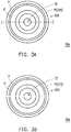
- FIG. 3A is a top view of the tapered optical needle of FIG. 1 .
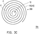
- FIG. 3B and FIG. 3C are top views of a tapered optical needle according to other embodiments of the disclosure.
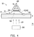
- FIG. 4 is a schematic diagram of a light source device having the tapered optical needle of FIG. 1 .
- the light source device 75 includes a tapered optical needle 50 and an excitation light source 300 used for emitting an exciting beam LB1 to the tapered optical needle 50, wherein the surface plasmon wave transport layer 200 is disposed on the curved surface S1.
- the surface plasmon wave transport layer 200 covers the first tip T1 and the curved surface S1 of the tapered light-transmissive needle 100.
- the surface plasmon wave transport layer 200 has a curved slit structure 210.
- the curved slit structure 210 is actually a gap, as shown in FIG. 2 . Therefore, the internal tapered light-transmissive needle 100 may simultaneously contact the surface plasmon wave transport layer 200 and air through the gap.
- the excitation light source 300 provides a radial polarized light entering the tapered light-transmissive needle 100 from the bottom 120, a surface plasmon wave is induced at the curved slit structure 210, and the surface plasmon wave is transported on an outer surface S2 of the surface plasmon wave transport layer 200 facing away from the tapered light-transmissive needle 100.
- a material of the tapered light-transmissive needle 100 includes silicon dioxide, for example, glass with a main component of silicon dioxide, and a material of the surface plasmon wave transport layer 200 may be metal, for example, gold, silver, aluminium, etc., which is adapted to a situation that the exciting beam LB1 is a visible light beam since the silicon dioxide is a transparent material for the visible light.
- the material of the tapered light-transmissive needle 100 includes silicon, for example, a main component thereof is silicon, and the material of the surface plasmon wave transport layer 200 can be made of a semiconductor material, for example, silicon carbide, which is adapted to a situation that the exciting beam LB1 is an infrared light beam since silicon is a transparent material for the infrared light, though the disclosure is not limited thereto.
- a slit width B of the curved slit structure 210 satisfies: B ⁇ ⁇ 2 , in other words, the slit width B of the curved slit structure 210 is smaller than a half wavelength of the exciting beam LB1, by which a light transmittance of the slit is decreased to reduce noise, though the disclosure is not limited thereto.
- the curved slit structure 210 includes a plurality of curved portions P arranged from the first tip T1 to an edge R of the bottom 120 and located between the first tip T1 and the edge R of the bottom 120, and extending directions of the curved portions P are different to a direction from the first tip T1 to the edge R of the bottom 120.
- the curved slit structure 210 is a circularly symmetric ring-like slit extending to form a circle, as that shown in FIG. 3A .
- the curved slit structure 210 can be a continuous spiral slit (as shown in FIG.
- a distance between a center of an orthogonal projection of the curved slit structure 210 on a reference plane E parallel to the bottom 120 and an orthogonal projection of the first tip T1 on the reference plane E is not more than 1/10 of the wavelength of the exciting beam LB1 used for driving the tapered optical needle 50.
- a distance between an orthogonal projection of a center of the ring-shape structure on the reference plane E and an orthogonal projection of the first tip T1 on the reference plane E can be within 1/10 of the wavelength of the exciting beam LB1, though the disclosure is not limited thereto.
- one end of the surface plasmon wave transport layer 200 facing away from the first tip T1 is a second tip T2, and among the curved portions P arranged from the first tip T1 of the tapered light-transmissive needle 100 to the edge R of the bottom 120, a distance between the second tip T2 and the curved portion P closest to the second tip T2 and distances between the adjacent curved portions P are all different.
- the distances between the adjacent curved portions P arranged from the first tip T to the edge R of the bottom 120 are specific distances, and the distances are different to each other, so as to produce a surface plasmon resonance.
- the curved portions P are located at the positions producing the surface plasmon resonance at the outer surface S2 of the surface plasmon wave transport layer 200.
- the actual positions of the curved portions P are determined one-by-one outward from the center by a two-dimensional simulation program according to an appearance of the outer surface S2 of the curved slit structure 210, and then an optimal electromagnetic field strength produced at the second tip T2 is simulated by a three-dimensional simulation program.
- a distance L1 between the second tip T2 and the curved portion P closest to the second tip T2 is 10 times the half wavelength of the surface plasmon wave; a distance L2 between the curved portion P closest to the second tip T2 and the curved portion P secondly closest to the second tip T2 is 6 times the half wavelength of the surface plasmon wave; a distance L3 between the curved portion P secondly closest to the second tip T2 and the curved portion P thirdly closest to the second tip T2 is 3 times the half wavelength of the surface plasmon wave; a distance L4 between the curved portion P thirdly closest to the second tip T2 and the curved portion P fourthly closest to the second tip T2 is 4 times the half wavelength of the surface plasmon wave; a distance L5 between the curved portion P fourthly closest to the second tip T2 and the curved portion P fifthly closest to the second tip T2 is one time the half wavelength of the surface plasmon wave; and a distance L6 between the curved portion P fifthly closest to the second tip T2 is
- the distance between the second tip T2 and the curved portion P closest to the second tip T2 and the distances between every adjacent curved portions P can be positive integer multiples of the half wavelength of the excited surface plasmon wave.
- FIG. 5A and FIG. 5B are respectively schematic diagrams of cross sections of a radial polarized light and a linear polarized light.
- the tapered optical needle 50 of the disclosure is driven by the exciting beam LB1, wherein the exciting beam LB1 may be a radial polarized light (as shown in FIG. 5A ), and enters the tapered optical needle 50 for driving the same from the bottom 120 towards the first tip T1 along a direction perpendicular to the reference plane E.
- a polarization direction K1 of each part of the radial polarized light surrounding a central axis of the beam is on a radial direction perpendicular to the central axis, as shown in FIG. 5A .
- the exciting beam LB1 can also be a linear polarized light (as shown in FIG. 5B ), which enters the tapered optical needle 50 for driving the same from the bottom 120 towards the first tip T1 along a direction including an angle with the reference plane E.
- an incident direction of the exciting beam LB1 implemented by the linear polarized light is not parallel to a direction from the first tip T1 to a center of the bottom 120, though the disclosure is not limited thereto.
- a polarization direction K2 of the linear polarized light is perpendicular to the central axis of the beam, and the polarization direction K2 of the entire beam is toward the same direction.
- the curved slit structure 210 may induce the surface plasmon wave on the surface plasmon wave transport layer 200, and the surface plasmon wave is focused at the second tip T2 to form a nanoscale light source LB2.
- the exciting beam LB1 enters the tapered light-transmissive needle 100
- the surface plasmon wave is induced at the curved slit structure 210, and the surface plasmon wave is transported on the outer surface S2 of the surface plasmon wave transport layer 200 to form the surface plasmon resonance.
- the surface plasmon wave is focused at the second tip T2 to form the nanoscale light source LB2.
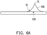
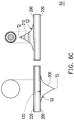
- FIG. 6A to FIG. 6C illustrate a fabrication flow of a tapered optical needle according to an embodiment of the disclosure.
- the tapered light-transmissive needle 100 connected to a substrate is prepared, wherein the tapered light-transmissive needle 100 can be fabricated by using silicon dioxide through a non-isotropic etching process, and the tapered light-transmissive needle 100 includes the first tip T1 and the bottom 120, as shown in FIG. 6A .
- a reflection layer 220 and the surface plasmon wave transport layer 200 are respectively coated on the tapered light-transmissive needle 100 in a sputtering manner along a direction from the bottom 120 to the first tip T1 and a direction from the first tip T1 to the bottom 120 (a sputtering direction A shown in FIG. 6B ).
- a material of the coated reflection layer 220 and the coated surface plasmon wave transport layer 200 is metal, for example, gold, as shown in FIG. 6B , though the disclosure is not limited thereto.
- a focused ion beam is adopted to hollow the substrate at the bottom 120 to facilitate the exciting beam to pass.
- the substrate at the bottom 120 is not hollowed such that the tapered optical needle 50 can be used as a probe, wherein the reflection layer 220 may serve as a reflection surface for reflecting, for example, a laser beam in an atomic force microscope (AFM).
- the reflection layer 220 may serve as a reflection surface for reflecting, for example, a laser beam in an atomic force microscope (AFM).
- the focused ion beam is adopted to form the curved slit structure 210 on the curved surface S1, so as to complete the tapered optical needle 50 of the disclosure, as shown in FIG. 6C .
- FIG. 7 is a variation broken line diagram of the number of ring-like structures of a tapered optical needle and a light intensity enhancement factor according to an embodiment of the disclosure.
- FIG. 8 is a variation curve diagram of a light intensity enhancement of a nano-light source of the light source device of FIG. 4 and a distance from the tip.
- the actual position thereof is determined by the two-dimensional simulation program by adopting the radial polarized light according to a plasmon wave resonance condition.
- E F E tip E illumination 2 (enhancement factor), wherein E tip refers to an electric field at the second tip T2, and E illuminaiton refers to an electric field of the exciting beam LB1, as shown by a left scale of FIG. 7 , wherein the light intensity enhancement factor is increased along with increase of the number of the ring-like structures, and the more the number of the ring-like structures is increased, the increase of the light intensity enhancement becomes flatter.
- a curve 420 in FIG. 7 represents a light intensity enhancement efficiency E FN E F N ⁇ 1 (wherein E FN represents the E F value (i.e.
- the light intensity enhancement factor) in case of the N ring-like structures obtained when the curved slit structure 210 has N ring-like structures and when the curved slit structure 210 has (N-1) ring-like structures, and the enhancement efficiency thereof is gradually flattened along with increase of the number of the ring-like structures, as shown by a right scale of FIG. 7 .
- the light intensity enhancement efficiency obtained in case that the number of the ring-like structure is 1 and the number of the ring-like structure is 0 is about 13
- the light intensity enhancement efficiency obtained in case that the number of the ring-like structure is 2 and the number of the ring-like structure is 1 is about 2. Therefore, according to the result of FIG.
- an electric field enhancement of a general opening-type probe is about 100 times, and the light intensity enhancement of the tampered optical needle 50 manufactured according to the disclosure may reach about 4000 times (as shown in FIG. 8 ), which has an enhancement effect 40 times that of the general opening-type probe, and at the second tip T2, the electric field enhancement may even reach 7000 times.
- a full width at half maximum (FWHM) W thereof is about 7.8 nm according to the relationship between the light intensity enhancement and the distance from the second tip T2, and since the probe used in the disclosure is a non-opening-type probe, a radius of the needle tip thereof can be reduced to improve a spatial resolution.
- the size of the nanoscale light source LB2 can be regarded as 7.8 nm, and the optical resolution of the tapered optical needle 50 of the disclosure may reach a size smaller than 10 nm.
- the manufacturing process of the tapered optical needle 50 of the disclosure may be further combined with a microelectromechanical systems (MEMS) technique, so that the tapered optical needle 50 of the disclosure has higher stability compared to the conventional optical probe, and has higher applicability in commercial application.
- the tapered optical needle 50 of the disclosure can also be applied to a material detection field to serve as a probe, for example, applied to a Near-field scanning optical microscope (NSOM), a tip enhancement Raman spectroscopy (TERS) or a light-emitting diode device to use as an optical coupling structure.
- NOM Near-field scanning optical microscope
- TMS tip enhancement Raman spectroscopy
- the tapered optical needle 50 in the embodiments of the disclosure may receive an external light signal through the second tip T2, so as to improve a measuring resolution.
- the surface plasmon wave transport layer has the curved slit structure, so as to induce a surface plasmon wave on the surface plasmon wave transport layer.
- the tapered optical needle in the embodiments of the disclosure is adapted to transport the surface plasmon wave to the tip of the tapered optical needle, and form a nanofocus effect at the tip to produce a high efficiency nanoscale light source, and may improve the resolution and light emitting gain.
- the tapered optical needle in the embodiments of the disclosure is adapted to receive an optical signal from the tip of the tapered optical needle, so as to improve a measuring resolution.
Landscapes
- Health & Medical Sciences (AREA)
- Physics & Mathematics (AREA)
- General Physics & Mathematics (AREA)
- Nuclear Medicine, Radiotherapy & Molecular Imaging (AREA)
- General Health & Medical Sciences (AREA)
- Biochemistry (AREA)
- Analytical Chemistry (AREA)
- Chemical & Material Sciences (AREA)
- Life Sciences & Earth Sciences (AREA)
- Immunology (AREA)
- Pathology (AREA)
- Radiology & Medical Imaging (AREA)
- Optics & Photonics (AREA)
- Investigating, Analyzing Materials By Fluorescence Or Luminescence (AREA)
- Investigating Or Analysing Materials By Optical Means (AREA)
Abstract
Description
- The disclosure relates to an optical structure, and particularly relates to a tapered optical needle.
- Along with development of technology, sizes of materials and components have been reduced to a nanoscale, and people have entered a new nanotechnology era. In various nanotechnology developments, nano microscopy technique and nano manipulation technique have attracted extensive attention, and based on the aforementioned techniques, atoms, molecules or molecule arrangement can be controlled according to material characteristics, and new techniques applied to human life can be further created, for example, an optical lithography technique, a nanomaterial sensing technique, micro drag detection, DNA detection, etc. However, in development of optical technology, since an optical lens is limited by Abbe's diffraction limit, a size of a light source can only be about several hundreds of nanometers or more, which greatly limits the development of the optical technology. On the other hand, in the optical detection technique, since a difference between sizes of a light source and a nano substance is too large, efficiency of an interaction force between light and the nano substance is decreased, which causes inadequate sensitivity of the optical detection, for example, a weak Raman signal. Therefore, under the current nanotechnology development, it is one of the popular research trends to develop a stable nanometer light source.
- In the current nanotechnology development, research of surface plasmon occupies an important position. The surface plasmon is a collective electron gas resonance wave existing at the interface between a metal and a dielectric, and such resonance wave may produce an electromagnetic field nanofocus effect to form a nano light source through a specific structure design, wherein the nano light source has a nanoscale, and may produce a high efficiency interaction force with a substance with the nanoscale, so that sensitivity of the optical detection is improved to reach a single molecule level. In a daily life level, the nano light source technology can be applied to detect contaminants in environment and food such as plasticizers, environmental hormones, phosphates, etc., or applied to biomedical field detection, for example, non-dye based biological calibration, antigen detection, DNA synthesis, drug or biological screening and tissue testing, etc. Moreover, in the field of microscope, the nano light source technology can be combined with a tip enhanced Raman spectroscopy (TERS) method for applying to an atomic force microscope (AFM), in this way, such device has both of sensitivity of surface-enhanced Raman spectroscopy (SERS) and an ultra high spectral resolution provided by the AFM.
- In current development of nano light source structure, a front end of a needle-like structure of a probe is opened by 100 nm, and the nanoscale light source is produced at a near-field of the opening, though a light intensity of the nanoscale light source of such structure is limited by Bethe's theory, such that a light flux of the nano light source only has a light conversion efficiency of 10-5 to 10-7 to decrease a signal to noise ratio. In order to maintain an enough signal to noise ratio to decrease a measuring time or an lithography exposure time, an actual size of an aperture of such structure is about 50 to 100 nm, which results in a fact that the optical resolution is only 50 to 100 nm and a spatial resolution is greater than 100 nm.
- The disclosure is directed to a tapered optical needle, where a nano light source is produced at a tip thereof through an excitation light source, so as to improve a resolution and a light emitting gain, or an optical signal is received by the tip to improve a measuring resolution.
- An embodiment of the disclosure provides a tapered optical needle including a tapered light-transmissive needle and a surface plasmon wave transport layer. The tapered light-transmissive needle has a first tip, a bottom, and a curved surface connecting the first tip and the bottom. The surface plasmon wave transport layer is disposed on the curved surface and covers the first tip, wherein the surface plasmon wave transport layer has a curved slit structure. The curved slit structure includes a plurality of curved portions arranged from the first tip to an edge of the bottom and located between the first tip and the edge of the bottom, and extending directions of the curved portions are different to a direction from the first tip to the edge of the bottom.
- In the tapered optical needle of the embodiment of the disclosure, the surface plasmon wave transport layer has the curved slit structure, so as to induce a surface plasmon wave on the surface plasmon wave transport layer. In this way, the tapered optical needle of the embodiment of the disclosure is adapted to transport the surface plasmon wave to the tip of the tapered optical needle, and form a nanofocus effect at the tip to produce a high efficiency nanoscale light source, so as to improve the resolution and light emitting gain. Alternatively, the tapered optical needle of the disclosure is adapted to receive an optical signal from the tip of the tapered optical needle, so as to improve a measuring resolution.
- In order to make the aforementioned and other features and advantages of the disclosure comprehensible, several exemplary embodiments accompanied with figures are described in detail below.
-
-
FIG. 1 is a side view of a tapered optical needle according to an embodiment of the disclosure. -
FIG. 2 is a cross-sectional view of the tapered optical needle ofFIG. 1 . -
FIG. 3A is a top view of the tapered optical needle ofFIG. 1 . -
FIG. 3B andFIG. 3C are top views of a tapered optical needle according to another embodiment. -
FIG. 4 is a schematic diagram of a light source device having the tapered optical needle ofFIG. 1 . -
FIG. 5A and FIG. 5B are respectively schematic diagrams of cross sections of a radial polarized light and a linear polarized light. -
FIG. 6A to FIG. 6C illustrate a fabrication flow of a tapered optical needle according to an embodiment of the disclosure. -
FIG. 7 is a variation broken line diagram of the number of ring-like structures of a tapered optical needle and a light intensity enhancement factor according to an embodiment of the disclosure. -
FIG. 8 is a variation curve diagram of a light intensity enhancement of a nano-light source of the light source device ofFIG. 4 and a distance from the tip. -
FIG. 1 is a side view of a tapered optical needle according to an embodiment of the disclosure.FIG. 2 is a cross-sectional view of the tapered optical needle ofFIG. 1 . Referring toFIG. 1 and FIG. 2 , in an embodiment of the disclosure, the taperedoptical needle 50 includes a tapered light-transmissive needle 100 and a surface plasmonwave transport layer 200. The tapered light-transmissive needle 100 has a first tip T1, abottom 120, and a curved surface S1 connecting the first tip T1 and thebottom 120. To be specific, the tapered light-transmissive needle 100 of the present embodiment is a circularly symmetric tapered structure, and the curved surface S1 is a tapered surface of the tapered light-transmissive needle 100. The tapered surface can be a quasi-parabolic surface, a conic surface, or other circularly symmetric tapered curved surfaces, and in the present embodiment, the curved surface S1 is, for example, a quasi-parabolic surface, as shown inFIG. 1 , though the disclosure is not limited thereto. -
FIG. 3A is a top view of the tapered optical needle ofFIG. 1 .FIG. 3B andFIG. 3C are top views of a tapered optical needle according to other embodiments of the disclosure.FIG. 4 is a schematic diagram of a light source device having the tapered optical needle ofFIG. 1 . Referring toFIG. 2 to FIG. 4 , in the present embodiment, thelight source device 75 includes a taperedoptical needle 50 and anexcitation light source 300 used for emitting an exciting beam LB1 to the taperedoptical needle 50, wherein the surface plasmonwave transport layer 200 is disposed on the curved surface S1. To be specific, the surface plasmonwave transport layer 200 covers the first tip T1 and the curved surface S1 of the tapered light-transmissive needle 100. The surface plasmonwave transport layer 200 has acurved slit structure 210. To be specific, thecurved slit structure 210 is actually a gap, as shown inFIG. 2 . Therefore, the internal tapered light-transmissive needle 100 may simultaneously contact the surface plasmonwave transport layer 200 and air through the gap. When theexcitation light source 300 provides a radial polarized light entering the tapered light-transmissive needle 100 from thebottom 120, a surface plasmon wave is induced at thecurved slit structure 210, and the surface plasmon wave is transported on an outer surface S2 of the surface plasmonwave transport layer 200 facing away from the tapered light-transmissive needle 100. In the present embodiment, a material of the tapered light-transmissive needle 100 includes silicon dioxide, for example, glass with a main component of silicon dioxide, and a material of the surface plasmonwave transport layer 200 may be metal, for example, gold, silver, aluminium, etc., which is adapted to a situation that the exciting beam LB1 is a visible light beam since the silicon dioxide is a transparent material for the visible light. In other embodiments, the material of the tapered light-transmissive needle 100 includes silicon, for example, a main component thereof is silicon, and the material of the surface plasmonwave transport layer 200 can be made of a semiconductor material, for example, silicon carbide, which is adapted to a situation that the exciting beam LB1 is an infrared light beam since silicon is a transparent material for the infrared light, though the disclosure is not limited thereto. - Moreover, in the present embodiment, a thickness of the surface plasmon
wave transport layer 200 is greater than a penetration depth D that the exciting beam LB1 penetrates through the surface plasmonwave transport layer 200, and the penetration depth D satisfies:

wave transport layer 200. A slit width B of thecurved slit structure 210 satisfies:
curved slit structure 210 is smaller than a half wavelength of the exciting beam LB1, by which a light transmittance of the slit is decreased to reduce noise, though the disclosure is not limited thereto. - On the other hand, the
curved slit structure 210 includes a plurality of curved portions P arranged from the first tip T1 to an edge R of thebottom 120 and located between the first tip T1 and the edge R of thebottom 120, and extending directions of the curved portions P are different to a direction from the first tip T1 to the edge R of thebottom 120. To be specific, thecurved slit structure 210 is a circularly symmetric ring-like slit extending to form a circle, as that shown inFIG. 3A . However, in other embodiments, viewing from a top view, thecurved slit structure 210 can be a continuous spiral slit (as shown inFIG. 3C ), or can be constructed by a plurality of C-shape ring-like slits with different radiuses by taking the first tip T1 as a common center. In the present embodiment, the ring-like slit is taken as an example for description, as shown inFIG. 3A , though the disclosure is not limited thereto. Besides, in other embodiments, a distance between a center of an orthogonal projection of thecurved slit structure 210 on a reference plane E parallel to the bottom 120 and an orthogonal projection of the first tip T1 on the reference plane E is not more than 1/10 of the wavelength of the exciting beam LB1 used for driving the taperedoptical needle 50. For example, taking the ring-shape structure as an example, a distance between an orthogonal projection of a center of the ring-shape structure on the reference plane E and an orthogonal projection of the first tip T1 on the reference plane E can be within 1/10 of the wavelength of the exciting beam LB1, though the disclosure is not limited thereto. - On the other hand, one end of the surface plasmon
wave transport layer 200 facing away from the first tip T1 is a second tip T2, and among the curved portions P arranged from the first tip T1 of the tapered light-transmissive needle 100 to the edge R of the bottom 120, a distance between the second tip T2 and the curved portion P closest to the second tip T2 and distances between the adjacent curved portions P are all different. In brief, the distances between the adjacent curved portions P arranged from the first tip T to the edge R of the bottom 120 are specific distances, and the distances are different to each other, so as to produce a surface plasmon resonance. Namely, the curved portions P are located at the positions producing the surface plasmon resonance at the outer surface S2 of the surface plasmonwave transport layer 200. In detail, the actual positions of the curved portions P are determined one-by-one outward from the center by a two-dimensional simulation program according to an appearance of the outer surface S2 of thecurved slit structure 210, and then an optimal electromagnetic field strength produced at the second tip T2 is simulated by a three-dimensional simulation program. For example, a distance L1 between the second tip T2 and the curved portion P closest to the second tip T2 is 10 times the half wavelength of the surface plasmon wave; a distance L2 between the curved portion P closest to the second tip T2 and the curved portion P secondly closest to the second tip T2 is 6 times the half wavelength of the surface plasmon wave; a distance L3 between the curved portion P secondly closest to the second tip T2 and the curved portion P thirdly closest to the second tip T2 is 3 times the half wavelength of the surface plasmon wave; a distance L4 between the curved portion P thirdly closest to the second tip T2 and the curved portion P fourthly closest to the second tip T2 is 4 times the half wavelength of the surface plasmon wave; a distance L5 between the curved portion P fourthly closest to the second tip T2 and the curved portion P fifthly closest to the second tip T2 is one time the half wavelength of the surface plasmon wave; and a distance L6 between the curved portion P fifthly closest to the second tip T2 and the curved portion P sixthly closest to the second tip T2 is 2 times the half wavelength of the surface plasmon wave, as shown inFIG. 2 (only L1 and L2 are illustrated). In other words, the distance between the second tip T2 and the curved portion P closest to the second tip T2 and the distances between every adjacent curved portions P can be positive integer multiples of the half wavelength of the excited surface plasmon wave. On the other hand, the distance L between the second tip T2 and each of the curved portions P arranged from the second tip T2 to the edge R of the bottom 120 in thecurved slit structure 210 satisfies:


transmissive needle 100. The position setting of thecurved slit structure 210 and the curved portions P therein optimized by the simulation programs may greatly improve a focusing effect of the taperedoptical needle 50, and an electric field enhancement strength thereof is far greater than that of a general mainstream optical probe. -
FIG. 5A and FIG. 5B are respectively schematic diagrams of cross sections of a radial polarized light and a linear polarized light. Referring toFIG. 4 to FIG. 5B , the taperedoptical needle 50 of the disclosure is driven by the exciting beam LB1, wherein the exciting beam LB1 may be a radial polarized light (as shown inFIG. 5A ), and enters the taperedoptical needle 50 for driving the same from the bottom 120 towards the first tip T1 along a direction perpendicular to the reference plane E. A polarization direction K1 of each part of the radial polarized light surrounding a central axis of the beam is on a radial direction perpendicular to the central axis, as shown inFIG. 5A . In other embodiments, the exciting beam LB1 can also be a linear polarized light (as shown inFIG. 5B ), which enters the taperedoptical needle 50 for driving the same from the bottom 120 towards the first tip T1 along a direction including an angle with the reference plane E. In other words, an incident direction of the exciting beam LB1 implemented by the linear polarized light is not parallel to a direction from the first tip T1 to a center of the bottom 120, though the disclosure is not limited thereto. A polarization direction K2 of the linear polarized light is perpendicular to the central axis of the beam, and the polarization direction K2 of the entire beam is toward the same direction. When the taperedoptical needle 50 is driven by the exciting beam LB1, thecurved slit structure 210 may induce the surface plasmon wave on the surface plasmonwave transport layer 200, and the surface plasmon wave is focused at the second tip T2 to form a nanoscale light source LB2. To be specific, when the exciting beam LB1 enters the tapered light-transmissive needle 100, the surface plasmon wave is induced at thecurved slit structure 210, and the surface plasmon wave is transported on the outer surface S2 of the surface plasmonwave transport layer 200 to form the surface plasmon resonance. Finally, the surface plasmon wave is focused at the second tip T2 to form the nanoscale light source LB2. -
FIG. 6A to FIG. 6C illustrate a fabrication flow of a tapered optical needle according to an embodiment of the disclosure. Referring toFIG. 6A to FIG. 6C , in the fabrication steps of the taperedoptical needle 50 of the disclosure, first, the tapered light-transmissive needle 100 connected to a substrate is prepared, wherein the tapered light-transmissive needle 100 can be fabricated by using silicon dioxide through a non-isotropic etching process, and the tapered light-transmissive needle 100 includes the first tip T1 and the bottom 120, as shown inFIG. 6A . Then, areflection layer 220 and the surface plasmonwave transport layer 200 are respectively coated on the tapered light-transmissive needle 100 in a sputtering manner along a direction from the bottom 120 to the first tip T1 and a direction from the first tip T1 to the bottom 120 (a sputtering direction A shown inFIG. 6B ). In the present embodiment, a material of thecoated reflection layer 220 and the coated surface plasmonwave transport layer 200 is metal, for example, gold, as shown inFIG. 6B , though the disclosure is not limited thereto. Then, a focused ion beam is adopted to hollow the substrate at the bottom 120 to facilitate the exciting beam to pass. In other embodiments, the substrate at the bottom 120 is not hollowed such that the taperedoptical needle 50 can be used as a probe, wherein thereflection layer 220 may serve as a reflection surface for reflecting, for example, a laser beam in an atomic force microscope (AFM). On the other hand, according to position data of thecurved slit structure 210 determined in advance by using the two-dimensional simulation program according to the appearance of the curved surface S1 of the tapered light-transmissive needle 100, the focused ion beam is adopted to form thecurved slit structure 210 on the curved surface S1, so as to complete the taperedoptical needle 50 of the disclosure, as shown inFIG. 6C . -
FIG. 7 is a variation broken line diagram of the number of ring-like structures of a tapered optical needle and a light intensity enhancement factor according to an embodiment of the disclosure.FIG. 8 is a variation curve diagram of a light intensity enhancement of a nano-light source of the light source device ofFIG. 4 and a distance from the tip. Referring toFIG. 3A ,FIG. 7 and FIG. 8 , as described above, regarding thecurved slit structure 210 in the taperedoptical needle 50 of the disclosure, the actual position thereof is determined by the two-dimensional simulation program by adopting the radial polarized light according to a plasmon wave resonance condition. Acurve 410 inFIG. 7 represents a ratio between the light intensity enhancement corresponding to the number of the ring-like structures in thecurved slit structure 210 and an intensity enhancement of the exciting beam LB1:
FIG. 7 , wherein the light intensity enhancement factor is increased along with increase of the number of the ring-like structures, and the more the number of the ring-like structures is increased, the increase of the light intensity enhancement becomes flatter. For example, when the number of the ring-like structures is 1, the light intensity enhancement factor EF1 thereof is about 30, and when the number of the ring-like structures is 2, the light intensity enhancement factor EF2 thereof is about 50, so that the whole light intensity enhancement can be increased by increasing the number of the ring-like structures, as shown by thecurve 410 ofFIG. 7 . On the other hand, acurve 420 inFIG. 7 represents a light intensity enhancement efficiency
curved slit structure 210 has N ring-like structures and when thecurved slit structure 210 has (N-1) ring-like structures, and the enhancement efficiency thereof is gradually flattened along with increase of the number of the ring-like structures, as shown by a right scale ofFIG. 7 . For example, the light intensity enhancement efficiency obtained in case that the number of the ring-like structure is 1 and the number of the ring-like structure is 0 is about 13, and the light intensity enhancement efficiency obtained in case that the number of the ring-like structure is 2 and the number of the ring-like structure is 1 is about 2. Therefore, according to the result ofFIG. 7 , it is learned that a difference between an enhancement effect of the taperedoptical needle 50 with 7 ring-like structures and an enhancement effect of the taperedoptical needle 50 with 6 ring-like structures is not large, so that the optimized taperedoptical needle 50 with 6 ring-like structures has reach optical field intensity enhancement optimization. It should be noted that an electric field enhancement of a general opening-type probe is about 100 times, and the light intensity enhancement of the tamperedoptical needle 50 manufactured according to the disclosure may reach about 4000 times (as shown inFIG. 8 ), which has an enhancement effect 40 times that of the general opening-type probe, and at the second tip T2, the electric field enhancement may even reach 7000 times. On the other hand, regarding the nanoscale light source LB2 produced at the second tip T2, it is learned that a full width at half maximum (FWHM) W thereof is about 7.8 nm according to the relationship between the light intensity enhancement and the distance from the second tip T2, and since the probe used in the disclosure is a non-opening-type probe, a radius of the needle tip thereof can be reduced to improve a spatial resolution. In other words, the size of the nanoscale light source LB2 can be regarded as 7.8 nm, and the optical resolution of the taperedoptical needle 50 of the disclosure may reach a size smaller than 10 nm. - The manufacturing process of the tapered
optical needle 50 of the disclosure may be further combined with a microelectromechanical systems (MEMS) technique, so that the taperedoptical needle 50 of the disclosure has higher stability compared to the conventional optical probe, and has higher applicability in commercial application. The taperedoptical needle 50 of the disclosure can also be applied to a material detection field to serve as a probe, for example, applied to a Near-field scanning optical microscope (NSOM), a tip enhancement Raman spectroscopy (TERS) or a light-emitting diode device to use as an optical coupling structure. Namely, the taperedoptical needle 50 in the embodiments of the disclosure may receive an external light signal through the second tip T2, so as to improve a measuring resolution. - In summary, in the tapered optical needle in the embodiments of the disclosure, the surface plasmon wave transport layer has the curved slit structure, so as to induce a surface plasmon wave on the surface plasmon wave transport layer. In this way, the tapered optical needle in the embodiments of the disclosure is adapted to transport the surface plasmon wave to the tip of the tapered optical needle, and form a nanofocus effect at the tip to produce a high efficiency nanoscale light source, and may improve the resolution and light emitting gain. Alternatively, the tapered optical needle in the embodiments of the disclosure is adapted to receive an optical signal from the tip of the tapered optical needle, so as to improve a measuring resolution.
Claims (13)
- A tapered optical needle (50, 50a, 50b, 50c), comprising:a tapered light-transmissive needle (100), having a first tip (T1), a bottom (120), and a curved surface (S1) connecting the first tip (T1) and the bottom (120); anda surface plasmon wave transport layer (200), disposed on the curved surface (S1) and covering the first tip (T1), wherein the surface plasmon wave transport layer (200) has a curved slit structure (210), the curved slit structure (210) comprises a plurality of curved portions (P) arranged from the first tip (T1) to an edge (R) of the bottom (120) and located between the first tip (T1) and the edge (R) of the bottom (120), and extending directions of the curved portions (P) are different to a direction from the first tip (T1) to the edge (R) of the bottom (120).
- The tapered optical needle (50, 50a, 50b, 50c) as claimed in claim 1, wherein the tapered optical needle (50, 50a, 50b, 50c) is driven by an excitation light source (300), and a surface plasmon wave is induced at the curved slit structure (210), and the curved portions (P) are located at positions producing a surface plasmon resonance at a surface of the surface plasmon wave transport layer (200) facing away from the tapered light-transmissive needle (100), and a nanoscale light source (LB2) is formed by focusing at one end of the surface plasmon wave transport layer (200) facing away from the first tip (T1).
- The tapered optical needle (50, 50a, 50b, 50c) as claimed in claim 2, wherein the excitation light source (300) provides a radial polarized light to drive the tapered optical needle (50, 50a, 50b, 50c).
- The tapered optical needle (50, 50a, 50b, 50c) as claimed in claim 2, wherein the excitation light source (300) provides a linear polarized light to the tapered optical needle (50, 50a, 50b, 50c) to drive the tapered optical needle (50, 50a, 50b, 50c), and an incident direction of the linear polarized light is not parallel to a direction from the first tip (T1) to a center of the bottom (120).
- The tapered optical needle (50, 50a, 50b, 50c) as claimed in claim 1, wherein the tapered light-transmissive needle (100) is a circularly symmetric tapered structure.
- The tapered optical needle (50, 50a, 50b, 50c) as claimed in claim 5, wherein the curved surface (S1) is a quasi-parabolic surface.
- The tapered optical needle (50, 50a, 50b, 50c) as claimed in claim 1, wherein a material of the tapered light-transmissive needle (100) comprises silicon dioxide.
- The tapered optical needle (50, 50a, 50b, 50c) as claimed in claim 7, wherein a material of the surface plasmon wave transport layer (200) is metal.
- The tapered optical needle (50, 50a, 50b, 50c) as claimed in claim 1, wherein a material of the tapered light-transmissive needle (100) comprises silicon.
- The tapered optical needle (50, 50a, 50b, 50c) as claimed in claim 9, wherein the surface plasmon wave transport layer (200) is a semiconductor material.
- The tapered optical needle (50, 50a, 50b, 50c) as claimed in claim 1, wherein one end of the surface plasmon wave transport layer (200) facing away from the first tip (T1) is a second tip (T2), a distance between the second tip (T2) and the curved portion closest to the second tip (T2) among the curved portions (P) and distances between the adjacent curved portions (P) are all different.
- The tapered optical needle (50, 50a, 50b, 50c) as claimed in claim 11, wherein the tapered optical needle (50, 50a, 50b, 50c) is driven by an excitation light source (300), a distance L between the second tip (T2) and each of the curved portions (P) arranged from the second tip (T2) to the edge (R) of the bottom (120) in the curved slit structure (210) satisfies:


- The tapered optical needle (50, 50a, 50b, 50c) as claimed in claim 1, wherein a distance between a center of an orthogonal projection of the curved slit structure (210) on a reference plane (E) parallel to the bottom (120) and an orthogonal projection of the first tip (T1) on the reference plane (E) is not more than 1/10 of a wavelength of an excitation light source (300) used for driving the tapered optical needle (50, 50a, 50b, 50c).
Applications Claiming Priority (2)
| Application Number | Priority Date | Filing Date | Title |
|---|---|---|---|
| US201662378684P | 2016-08-24 | 2016-08-24 | |
| TW105142127A TWI638991B (en) | 2016-08-24 | 2016-12-20 | Tapered optical needle |
Publications (2)
| Publication Number | Publication Date |
|---|---|
| EP3287823A1 true EP3287823A1 (en) | 2018-02-28 |
| EP3287823B1 EP3287823B1 (en) | 2020-11-18 |
Family
ID=58714898
Family Applications (1)
| Application Number | Title | Priority Date | Filing Date |
|---|---|---|---|
| EP17166975.7A Active EP3287823B1 (en) | 2016-08-24 | 2017-04-19 | Tapered optical needle |
Country Status (3)
| Country | Link |
|---|---|
| US (1) | US10088424B2 (en) |
| EP (1) | EP3287823B1 (en) |
| CN (1) | CN107782710B (en) |
Cited By (3)
| Publication number | Priority date | Publication date | Assignee | Title |
|---|---|---|---|---|
| CN110955054A (en) * | 2019-11-26 | 2020-04-03 | 中国科学院光电技术研究所 | A method for producing nano-optical needles based on angularly polarized light |
| CN111721750A (en) * | 2020-06-23 | 2020-09-29 | 深圳大学 | Method and device for enhancing TERS signal in non-contact mode of atomic force microscope |
| CN111999904A (en) * | 2020-08-26 | 2020-11-27 | 东南大学 | Device for generating super-chiral optical field |
Families Citing this family (7)
| Publication number | Priority date | Publication date | Assignee | Title |
|---|---|---|---|---|
| US20160026275A1 (en) * | 2014-07-23 | 2016-01-28 | Verifone, Inc. | Data device including ofn functionality |
| US10332553B1 (en) * | 2017-12-29 | 2019-06-25 | Headway Technologies, Inc. | Double ridge near-field transducers |
| CN112964908B (en) * | 2021-02-04 | 2022-05-20 | 西安交通大学 | Scattering type tapered tip optical fiber probe for exciting and collecting near-field optical signals and working method thereof |
| CN112858729A (en) * | 2021-02-04 | 2021-05-28 | 西安交通大学 | Plasmon probe with conical optical fiber combined with semi-ring asymmetric nano slit and working method thereof |
| CN115524310B (en) * | 2022-09-19 | 2026-04-21 | 华南理工大学 | A spiral conical metal probe and its method for measuring the refractive index gradient in liquids. |
| CN115629068B (en) * | 2022-09-19 | 2025-06-24 | 华南理工大学 | A spiral cone metal probe and method for using the same for super-resolution near-field detection |
| CN120446056A (en) * | 2025-07-09 | 2025-08-08 | 中国科学院长春光学精密机械与物理研究所 | A method for generating linear light intensity optical needle and OCT system |
Citations (4)
| Publication number | Priority date | Publication date | Assignee | Title |
|---|---|---|---|---|
| US20050289576A1 (en) * | 2004-06-23 | 2005-12-29 | Seagate Technology Llc | Transducer for heat assisted magnetic recording |
| JP2007155453A (en) * | 2005-12-02 | 2007-06-21 | Ricoh Co Ltd | Optical fiber probe, inspection method and inspection apparatus |
| JP2007155454A (en) * | 2005-12-02 | 2007-06-21 | Ricoh Co Ltd | Optical fiber probe, inspection method and inspection apparatus |
| US20110321204A1 (en) * | 2010-06-23 | 2011-12-29 | The University Of Tokyo | Near-field optical microscope, near-field optical probe, and sample observation method |
Family Cites Families (20)
| Publication number | Priority date | Publication date | Assignee | Title |
|---|---|---|---|---|
| EP0924524A4 (en) * | 1996-09-06 | 1999-11-24 | Kanagawa Kagaku Gijutsu Akad | Optical fiber probe and its manufacturing method |
| JP3513448B2 (en) | 1999-11-11 | 2004-03-31 | キヤノン株式会社 | Optical probe |
| US6834027B1 (en) | 2000-02-28 | 2004-12-21 | Nec Laboratories America, Inc. | Surface plasmon-enhanced read/write heads for optical data storage media |
| US20050031278A1 (en) | 2003-05-16 | 2005-02-10 | Xiaolei Shi | Near-field sub-wavelength apertures |
| US7250598B2 (en) | 2004-01-02 | 2007-07-31 | Hollingsworth Russell E | Plasmon enhanced near-field optical probes |
| US7054528B2 (en) | 2004-04-14 | 2006-05-30 | Lucent Technologies Inc. | Plasmon-enhanced tapered optical fibers |
| KR100584987B1 (en) | 2004-10-11 | 2006-05-29 | 삼성전기주식회사 | Pyramid-shaped near field probe using surface plasmon wave |
| EP2033028A4 (en) * | 2006-05-31 | 2011-05-04 | Georgia Tech Res Inst | INTEGRATED DETECTION PROBES, METHODS OF MANUFACTURE AND METHODS OF USE THEREOF |
| DE102006040057A1 (en) | 2006-08-26 | 2008-02-28 | MAX-PLANCK-Gesellschaft zur Förderung der Wissenschaften e.V. | Device for concentration of polarized light of area substantially smaller than light wave length, has slots to support excitation of automatic concentrated surface plasmon resonance in metal shield by light radiation in chamber |
| US7772555B2 (en) * | 2007-02-05 | 2010-08-10 | Itn Energy Systems, Inc. | Plasmon coupling apparatus and method |
| IT1397108B1 (en) | 2008-09-23 | 2012-12-28 | Calmed S R L | PROCESS OF MANUFACTURE OF A PHOTONIC CRYSTAL DEVICE PROVIDED WITH A PLASMON WAVE GUIDE. |
| CN101447235B (en) | 2008-12-30 | 2010-09-15 | 安徽师范大学 | A localized surface plasmon resonance enhanced near-field optical probe |
| KR101117220B1 (en) | 2010-02-11 | 2012-03-20 | 연세대학교 산학협력단 | Method for fabricating The Nano Probe Array of Plasmonic Optical Apparatus |
| JP5560891B2 (en) * | 2010-05-13 | 2014-07-30 | セイコーエプソン株式会社 | Optical device and analyzer |
| KR20130136906A (en) | 2010-06-18 | 2013-12-13 | 글로 에이비 | Nanowire led structure and method for manufacturing the same |
| TWI461741B (en) | 2011-11-09 | 2014-11-21 | Univ Nat Taiwan | Optical head |
| US8921141B2 (en) | 2012-09-18 | 2014-12-30 | Glo Ab | Nanopyramid sized opto-electronic structure and method for manufacturing of same |
| CN103176283B (en) | 2013-03-29 | 2014-11-26 | 南开大学 | Micro-medium cone and nanometal grating-compounded optical probe |
| TW201511334A (en) | 2013-06-07 | 2015-03-16 | Glo Ab | Nanowire LED structure with decreased leakage and method of making same |
| CN103837709B (en) | 2014-03-04 | 2016-03-30 | 国家纳米科学中心 | A kind of surface plasma excimer strengthens needle point and needle point Enhancement Method |
-
2016
- 2016-12-25 US US15/390,525 patent/US10088424B2/en active Active
- 2016-12-29 CN CN201611243250.3A patent/CN107782710B/en active Active
-
2017
- 2017-04-19 EP EP17166975.7A patent/EP3287823B1/en active Active
Patent Citations (4)
| Publication number | Priority date | Publication date | Assignee | Title |
|---|---|---|---|---|
| US20050289576A1 (en) * | 2004-06-23 | 2005-12-29 | Seagate Technology Llc | Transducer for heat assisted magnetic recording |
| JP2007155453A (en) * | 2005-12-02 | 2007-06-21 | Ricoh Co Ltd | Optical fiber probe, inspection method and inspection apparatus |
| JP2007155454A (en) * | 2005-12-02 | 2007-06-21 | Ricoh Co Ltd | Optical fiber probe, inspection method and inspection apparatus |
| US20110321204A1 (en) * | 2010-06-23 | 2011-12-29 | The University Of Tokyo | Near-field optical microscope, near-field optical probe, and sample observation method |
Cited By (3)
| Publication number | Priority date | Publication date | Assignee | Title |
|---|---|---|---|---|
| CN110955054A (en) * | 2019-11-26 | 2020-04-03 | 中国科学院光电技术研究所 | A method for producing nano-optical needles based on angularly polarized light |
| CN111721750A (en) * | 2020-06-23 | 2020-09-29 | 深圳大学 | Method and device for enhancing TERS signal in non-contact mode of atomic force microscope |
| CN111999904A (en) * | 2020-08-26 | 2020-11-27 | 东南大学 | Device for generating super-chiral optical field |
Also Published As
| Publication number | Publication date |
|---|---|
| CN107782710A (en) | 2018-03-09 |
| US10088424B2 (en) | 2018-10-02 |
| US20180059025A1 (en) | 2018-03-01 |
| EP3287823B1 (en) | 2020-11-18 |
| CN107782710B (en) | 2020-08-11 |
Similar Documents
| Publication | Publication Date | Title |
|---|---|---|
| EP3287823B1 (en) | Tapered optical needle | |
| Wang et al. | Plasmonic nearfield scanning probe with high transmission | |
| Spesyvtseva et al. | Trapping in a material world | |
| Lindquist et al. | Plasmonic nanofocusing with a metallic pyramid and an integrated C-shaped aperture | |
| Zhang et al. | Local field enhancement of an infinite conical metal tip illuminated by a focused beam | |
| Lindquist et al. | Tip‐based plasmonics: squeezing light with metallic nanoprobes | |
| US8993339B2 (en) | Hybrid nanostructures for molecular analysis | |
| US8599486B2 (en) | Three dimensional sub-wavelength structure with surface plasmon energy matching properties | |
| CN102707342B (en) | Surface plasmon lens integrated with metal nano-cavity | |
| CN111896500A (en) | Refractive index sensor and method based on metal nanostructure and single-layer TMDS composite system | |
| Guillot et al. | Lithographied nanostructures as nanosensors | |
| Ye et al. | Optical and electrical mappings of surface plasmon cavity modes | |
| CN110926667A (en) | A pressure sensing device based on asymmetric periodic surface plasmon lattice resonance | |
| Guan et al. | Direct measurement of optical force induced by near-field plasmonic cavity using dynamic mode AFM | |
| Zhu et al. | Three-dimensional cavity-coupled metamaterials for plasmonic color and real-time colorimetric biosensors | |
| CN114235712A (en) | A single-molecule sensor based on an array of chiral metal nanostructures | |
| Chen et al. | Optimal plasmonic focusing with radial polarization | |
| Tuna et al. | Levitated plasmonic nanoantennas in an aqueous environment | |
| Nguyen et al. | Enhanced near-infrared fluorescent sensing using metal-dielectric-metal plasmonic array | |
| CN112857232B (en) | Long Range Optical Self-Reference Displacement Sensor | |
| Valev | Chiral nanomaterials and chiral light | |
| TWI638991B (en) | Tapered optical needle | |
| EP2876431B1 (en) | Substrate for the generation of surface plasmons and surface plasmon polaritons by means of an excitation radiation, method for the production of the substrate, and uses of the substrate | |
| Wang et al. | Unveiling the Loss Mode Enabled Tunable Plasmonic Chirality at Flat Metal Surface | |
| Denisyuk et al. | Tunable optical antennas based on metallic nanoshells with nanoknobs |
Legal Events
| Date | Code | Title | Description |
|---|---|---|---|
| PUAI | Public reference made under article 153(3) epc to a published international application that has entered the european phase |
Free format text: ORIGINAL CODE: 0009012 |
|
| STAA | Information on the status of an ep patent application or granted ep patent |
Free format text: STATUS: REQUEST FOR EXAMINATION WAS MADE |
|
| 17P | Request for examination filed |
Effective date: 20170419 |
|
| AK | Designated contracting states |
Kind code of ref document: A1 Designated state(s): AL AT BE BG CH CY CZ DE DK EE ES FI FR GB GR HR HU IE IS IT LI LT LU LV MC MK MT NL NO PL PT RO RS SE SI SK SM TR |
|
| AX | Request for extension of the european patent |
Extension state: BA ME |
|
| RBV | Designated contracting states (corrected) |
Designated state(s): AL AT BE BG CH CY CZ DE DK EE ES FI FR GB GR HR HU IE IS IT LI LT LU LV MC MK MT NL NO PL PT RO RS SE SI SK SM TR |
|
| STAA | Information on the status of an ep patent application or granted ep patent |
Free format text: STATUS: EXAMINATION IS IN PROGRESS |
|
| 17Q | First examination report despatched |
Effective date: 20190305 |
|
| RIC1 | Information provided on ipc code assigned before grant |
Ipc: G02B 6/122 20060101AFI20200408BHEP Ipc: G01N 21/65 20060101ALN20200408BHEP Ipc: G01Q 60/22 20100101ALI20200408BHEP |
|
| GRAP | Despatch of communication of intention to grant a patent |
Free format text: ORIGINAL CODE: EPIDOSNIGR1 |
|
| STAA | Information on the status of an ep patent application or granted ep patent |
Free format text: STATUS: GRANT OF PATENT IS INTENDED |
|
| INTG | Intention to grant announced |
Effective date: 20200616 |
|
| GRAS | Grant fee paid |
Free format text: ORIGINAL CODE: EPIDOSNIGR3 |
|
| GRAA | (expected) grant |
Free format text: ORIGINAL CODE: 0009210 |
|
| STAA | Information on the status of an ep patent application or granted ep patent |
Free format text: STATUS: THE PATENT HAS BEEN GRANTED |
|
| AK | Designated contracting states |
Kind code of ref document: B1 Designated state(s): AL AT BE BG CH CY CZ DE DK EE ES FI FR GB GR HR HU IE IS IT LI LT LU LV MC MK MT NL NO PL PT RO RS SE SI SK SM TR |
|
| REG | Reference to a national code |
Ref country code: GB Ref legal event code: FG4D |
|
| REG | Reference to a national code |
Ref country code: CH Ref legal event code: EP |
|
| REG | Reference to a national code |
Ref country code: IE Ref legal event code: FG4D |
|
| REG | Reference to a national code |
Ref country code: DE Ref legal event code: R096 Ref document number: 602017027614 Country of ref document: DE |
|
| REG | Reference to a national code |
Ref country code: AT Ref legal event code: REF Ref document number: 1336385 Country of ref document: AT Kind code of ref document: T Effective date: 20201215 |
|
| REG | Reference to a national code |
Ref country code: NL Ref legal event code: FP |
|
| REG | Reference to a national code |
Ref country code: AT Ref legal event code: MK05 Ref document number: 1336385 Country of ref document: AT Kind code of ref document: T Effective date: 20201118 |
|
| PG25 | Lapsed in a contracting state [announced via postgrant information from national office to epo] |
Ref country code: PT Free format text: LAPSE BECAUSE OF FAILURE TO SUBMIT A TRANSLATION OF THE DESCRIPTION OR TO PAY THE FEE WITHIN THE PRESCRIBED TIME-LIMIT Effective date: 20210318 Ref country code: RS Free format text: LAPSE BECAUSE OF FAILURE TO SUBMIT A TRANSLATION OF THE DESCRIPTION OR TO PAY THE FEE WITHIN THE PRESCRIBED TIME-LIMIT Effective date: 20201118 Ref country code: NO Free format text: LAPSE BECAUSE OF FAILURE TO SUBMIT A TRANSLATION OF THE DESCRIPTION OR TO PAY THE FEE WITHIN THE PRESCRIBED TIME-LIMIT Effective date: 20210218 Ref country code: FI Free format text: LAPSE BECAUSE OF FAILURE TO SUBMIT A TRANSLATION OF THE DESCRIPTION OR TO PAY THE FEE WITHIN THE PRESCRIBED TIME-LIMIT Effective date: 20201118 Ref country code: GR Free format text: LAPSE BECAUSE OF FAILURE TO SUBMIT A TRANSLATION OF THE DESCRIPTION OR TO PAY THE FEE WITHIN THE PRESCRIBED TIME-LIMIT Effective date: 20210219 |
|
| PG25 | Lapsed in a contracting state [announced via postgrant information from national office to epo] |
Ref country code: SE Free format text: LAPSE BECAUSE OF FAILURE TO SUBMIT A TRANSLATION OF THE DESCRIPTION OR TO PAY THE FEE WITHIN THE PRESCRIBED TIME-LIMIT Effective date: 20201118 Ref country code: BG Free format text: LAPSE BECAUSE OF FAILURE TO SUBMIT A TRANSLATION OF THE DESCRIPTION OR TO PAY THE FEE WITHIN THE PRESCRIBED TIME-LIMIT Effective date: 20210218 Ref country code: PL Free format text: LAPSE BECAUSE OF FAILURE TO SUBMIT A TRANSLATION OF THE DESCRIPTION OR TO PAY THE FEE WITHIN THE PRESCRIBED TIME-LIMIT Effective date: 20201118 Ref country code: LV Free format text: LAPSE BECAUSE OF FAILURE TO SUBMIT A TRANSLATION OF THE DESCRIPTION OR TO PAY THE FEE WITHIN THE PRESCRIBED TIME-LIMIT Effective date: 20201118 Ref country code: IS Free format text: LAPSE BECAUSE OF FAILURE TO SUBMIT A TRANSLATION OF THE DESCRIPTION OR TO PAY THE FEE WITHIN THE PRESCRIBED TIME-LIMIT Effective date: 20210318 Ref country code: AT Free format text: LAPSE BECAUSE OF FAILURE TO SUBMIT A TRANSLATION OF THE DESCRIPTION OR TO PAY THE FEE WITHIN THE PRESCRIBED TIME-LIMIT Effective date: 20201118 |
|
| REG | Reference to a national code |
Ref country code: ES Ref legal event code: FG2A Ref document number: 2836268 Country of ref document: ES Kind code of ref document: T3 Effective date: 20210624 |
|
| REG | Reference to a national code |
Ref country code: LT Ref legal event code: MG9D |
|
| PG25 | Lapsed in a contracting state [announced via postgrant information from national office to epo] |
Ref country code: HR Free format text: LAPSE BECAUSE OF FAILURE TO SUBMIT A TRANSLATION OF THE DESCRIPTION OR TO PAY THE FEE WITHIN THE PRESCRIBED TIME-LIMIT Effective date: 20201118 |
|
| PG25 | Lapsed in a contracting state [announced via postgrant information from national office to epo] |
Ref country code: SM Free format text: LAPSE BECAUSE OF FAILURE TO SUBMIT A TRANSLATION OF THE DESCRIPTION OR TO PAY THE FEE WITHIN THE PRESCRIBED TIME-LIMIT Effective date: 20201118 Ref country code: LT Free format text: LAPSE BECAUSE OF FAILURE TO SUBMIT A TRANSLATION OF THE DESCRIPTION OR TO PAY THE FEE WITHIN THE PRESCRIBED TIME-LIMIT Effective date: 20201118 Ref country code: EE Free format text: LAPSE BECAUSE OF FAILURE TO SUBMIT A TRANSLATION OF THE DESCRIPTION OR TO PAY THE FEE WITHIN THE PRESCRIBED TIME-LIMIT Effective date: 20201118 Ref country code: CZ Free format text: LAPSE BECAUSE OF FAILURE TO SUBMIT A TRANSLATION OF THE DESCRIPTION OR TO PAY THE FEE WITHIN THE PRESCRIBED TIME-LIMIT Effective date: 20201118 Ref country code: SK Free format text: LAPSE BECAUSE OF FAILURE TO SUBMIT A TRANSLATION OF THE DESCRIPTION OR TO PAY THE FEE WITHIN THE PRESCRIBED TIME-LIMIT Effective date: 20201118 Ref country code: RO Free format text: LAPSE BECAUSE OF FAILURE TO SUBMIT A TRANSLATION OF THE DESCRIPTION OR TO PAY THE FEE WITHIN THE PRESCRIBED TIME-LIMIT Effective date: 20201118 |
|
| REG | Reference to a national code |
Ref country code: DE Ref legal event code: R097 Ref document number: 602017027614 Country of ref document: DE |
|
| PG25 | Lapsed in a contracting state [announced via postgrant information from national office to epo] |
Ref country code: DK Free format text: LAPSE BECAUSE OF FAILURE TO SUBMIT A TRANSLATION OF THE DESCRIPTION OR TO PAY THE FEE WITHIN THE PRESCRIBED TIME-LIMIT Effective date: 20201118 |
|
| PLBE | No opposition filed within time limit |
Free format text: ORIGINAL CODE: 0009261 |
|
| STAA | Information on the status of an ep patent application or granted ep patent |
Free format text: STATUS: NO OPPOSITION FILED WITHIN TIME LIMIT |
|
| 26N | No opposition filed |
Effective date: 20210819 |
|
| PG25 | Lapsed in a contracting state [announced via postgrant information from national office to epo] |
Ref country code: AL Free format text: LAPSE BECAUSE OF FAILURE TO SUBMIT A TRANSLATION OF THE DESCRIPTION OR TO PAY THE FEE WITHIN THE PRESCRIBED TIME-LIMIT Effective date: 20201118 |
|
| PG25 | Lapsed in a contracting state [announced via postgrant information from national office to epo] |
Ref country code: MC Free format text: LAPSE BECAUSE OF FAILURE TO SUBMIT A TRANSLATION OF THE DESCRIPTION OR TO PAY THE FEE WITHIN THE PRESCRIBED TIME-LIMIT Effective date: 20201118 Ref country code: SI Free format text: LAPSE BECAUSE OF FAILURE TO SUBMIT A TRANSLATION OF THE DESCRIPTION OR TO PAY THE FEE WITHIN THE PRESCRIBED TIME-LIMIT Effective date: 20201118 |
|
| PG25 | Lapsed in a contracting state [announced via postgrant information from national office to epo] |
Ref country code: LU Free format text: LAPSE BECAUSE OF NON-PAYMENT OF DUE FEES Effective date: 20210419 |
|
| REG | Reference to a national code |
Ref country code: BE Ref legal event code: MM Effective date: 20210430 |
|
| PG25 | Lapsed in a contracting state [announced via postgrant information from national office to epo] |
Ref country code: CH Free format text: LAPSE BECAUSE OF NON-PAYMENT OF DUE FEES Effective date: 20210430 Ref country code: LI Free format text: LAPSE BECAUSE OF NON-PAYMENT OF DUE FEES Effective date: 20210430 |
|
| PG25 | Lapsed in a contracting state [announced via postgrant information from national office to epo] |
Ref country code: IE Free format text: LAPSE BECAUSE OF NON-PAYMENT OF DUE FEES Effective date: 20210419 |
|
| PG25 | Lapsed in a contracting state [announced via postgrant information from national office to epo] |
Ref country code: IS Free format text: LAPSE BECAUSE OF FAILURE TO SUBMIT A TRANSLATION OF THE DESCRIPTION OR TO PAY THE FEE WITHIN THE PRESCRIBED TIME-LIMIT Effective date: 20210318 |
|
| PG25 | Lapsed in a contracting state [announced via postgrant information from national office to epo] |
Ref country code: BE Free format text: LAPSE BECAUSE OF NON-PAYMENT OF DUE FEES Effective date: 20210430 |
|
| PG25 | Lapsed in a contracting state [announced via postgrant information from national office to epo] |
Ref country code: HU Free format text: LAPSE BECAUSE OF FAILURE TO SUBMIT A TRANSLATION OF THE DESCRIPTION OR TO PAY THE FEE WITHIN THE PRESCRIBED TIME-LIMIT; INVALID AB INITIO Effective date: 20170419 |
|
| PG25 | Lapsed in a contracting state [announced via postgrant information from national office to epo] |
Ref country code: CY Free format text: LAPSE BECAUSE OF FAILURE TO SUBMIT A TRANSLATION OF THE DESCRIPTION OR TO PAY THE FEE WITHIN THE PRESCRIBED TIME-LIMIT Effective date: 20201118 |
|
| PG25 | Lapsed in a contracting state [announced via postgrant information from national office to epo] |
Ref country code: MK Free format text: LAPSE BECAUSE OF FAILURE TO SUBMIT A TRANSLATION OF THE DESCRIPTION OR TO PAY THE FEE WITHIN THE PRESCRIBED TIME-LIMIT Effective date: 20201118 |
|
| PG25 | Lapsed in a contracting state [announced via postgrant information from national office to epo] |
Ref country code: MT Free format text: LAPSE BECAUSE OF FAILURE TO SUBMIT A TRANSLATION OF THE DESCRIPTION OR TO PAY THE FEE WITHIN THE PRESCRIBED TIME-LIMIT Effective date: 20201118 |
|
| PGFP | Annual fee paid to national office [announced via postgrant information from national office to epo] |
Ref country code: NL Payment date: 20250407 Year of fee payment: 9 |
|
| PGFP | Annual fee paid to national office [announced via postgrant information from national office to epo] |
Ref country code: DE Payment date: 20250328 Year of fee payment: 9 |
|
| PGFP | Annual fee paid to national office [announced via postgrant information from national office to epo] |
Ref country code: ES Payment date: 20250505 Year of fee payment: 9 |
|
| PGFP | Annual fee paid to national office [announced via postgrant information from national office to epo] |
Ref country code: IT Payment date: 20250430 Year of fee payment: 9 |
|
| PGFP | Annual fee paid to national office [announced via postgrant information from national office to epo] |
Ref country code: FR Payment date: 20250415 Year of fee payment: 9 |
|
| PG25 | Lapsed in a contracting state [announced via postgrant information from national office to epo] |
Ref country code: TR Free format text: LAPSE BECAUSE OF FAILURE TO SUBMIT A TRANSLATION OF THE DESCRIPTION OR TO PAY THE FEE WITHIN THE PRESCRIBED TIME-LIMIT Effective date: 20201118 |
|
| PGFP | Annual fee paid to national office [announced via postgrant information from national office to epo] |
Ref country code: GB Payment date: 20260331 Year of fee payment: 10 |