EP3286751B1 - Pixelstruktur, anzeigetafel und anzeigevorrichtung - Google Patents
Pixelstruktur, anzeigetafel und anzeigevorrichtung Download PDFInfo
- Publication number
- EP3286751B1 EP3286751B1 EP15849826.1A EP15849826A EP3286751B1 EP 3286751 B1 EP3286751 B1 EP 3286751B1 EP 15849826 A EP15849826 A EP 15849826A EP 3286751 B1 EP3286751 B1 EP 3286751B1
- Authority
- EP
- European Patent Office
- Prior art keywords
- pixel
- pixels
- cells
- adjacent
- red
- Prior art date
- Legal status (The legal status is an assumption and is not a legal conclusion. Google has not performed a legal analysis and makes no representation as to the accuracy of the status listed.)
- Active
Links
Images


Classifications
-
- G—PHYSICS
- G09—EDUCATION; CRYPTOGRAPHY; DISPLAY; ADVERTISING; SEALS
- G09G—ARRANGEMENTS OR CIRCUITS FOR CONTROL OF INDICATING DEVICES USING STATIC MEANS TO PRESENT VARIABLE INFORMATION
- G09G3/00—Control arrangements or circuits, of interest only in connection with visual indicators other than cathode-ray tubes
- G09G3/20—Control arrangements or circuits, of interest only in connection with visual indicators other than cathode-ray tubes for presentation of an assembly of a number of characters, e.g. a page, by composing the assembly by combination of individual elements arranged in a matrix no fixed position being assigned to or needed to be assigned to the individual characters or partial characters
- G09G3/2003—Display of colours
-
- H—ELECTRICITY
- H10—SEMICONDUCTOR DEVICES; ELECTRIC SOLID-STATE DEVICES NOT OTHERWISE PROVIDED FOR
- H10K—ORGANIC ELECTRIC SOLID-STATE DEVICES
- H10K59/00—Integrated devices, or assemblies of multiple devices, comprising at least one organic light-emitting element covered by group H10K50/00
- H10K59/30—Devices specially adapted for multicolour light emission
- H10K59/35—Devices specially adapted for multicolour light emission comprising red-green-blue [RGB] subpixels
- H10K59/352—Devices specially adapted for multicolour light emission comprising red-green-blue [RGB] subpixels the areas of the RGB subpixels being different
-
- H—ELECTRICITY
- H10—SEMICONDUCTOR DEVICES; ELECTRIC SOLID-STATE DEVICES NOT OTHERWISE PROVIDED FOR
- H10K—ORGANIC ELECTRIC SOLID-STATE DEVICES
- H10K59/00—Integrated devices, or assemblies of multiple devices, comprising at least one organic light-emitting element covered by group H10K50/00
- H10K59/30—Devices specially adapted for multicolour light emission
- H10K59/35—Devices specially adapted for multicolour light emission comprising red-green-blue [RGB] subpixels
- H10K59/353—Devices specially adapted for multicolour light emission comprising red-green-blue [RGB] subpixels characterised by the geometrical arrangement of the RGB subpixels
-
- G—PHYSICS
- G09—EDUCATION; CRYPTOGRAPHY; DISPLAY; ADVERTISING; SEALS
- G09G—ARRANGEMENTS OR CIRCUITS FOR CONTROL OF INDICATING DEVICES USING STATIC MEANS TO PRESENT VARIABLE INFORMATION
- G09G2300/00—Aspects of the constitution of display devices
- G09G2300/04—Structural and physical details of display devices
- G09G2300/0439—Pixel structures
- G09G2300/0452—Details of colour pixel setup, e.g. pixel composed of a red, a blue and two green components
-
- G—PHYSICS
- G09—EDUCATION; CRYPTOGRAPHY; DISPLAY; ADVERTISING; SEALS
- G09G—ARRANGEMENTS OR CIRCUITS FOR CONTROL OF INDICATING DEVICES USING STATIC MEANS TO PRESENT VARIABLE INFORMATION
- G09G2300/00—Aspects of the constitution of display devices
- G09G2300/04—Structural and physical details of display devices
- G09G2300/0439—Pixel structures
- G09G2300/0465—Improved aperture ratio, e.g. by size reduction of the pixel circuit, e.g. for improving the pixel density or the maximum displayable luminance or brightness
Definitions
- the present disclosure generally relates to the field of display technologies and, more particularly, relates to a pixel structure, a configuring method of the pixel structure, and a display panel including the pixel structure, and a display apparatus including the display panel.
- a conventional display device is configured with a plurality of pixels. Each pixel includes at least three pixels of different colors. Typically, a pixel includes three pixels in red, green and blue.
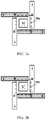
- the pixel arrangement in the conventional display devices includes array arrangement, mosaic arrangement and Bayer arrangement, as shown in FIGS. 1a-1c .
- the pixel arrangement is illustrated in accompanying figures with three pixels representing different colors ABC.
- FIG. 1a shows an array arrangement. Three pixels of ABC colors are alternately arranged in the same row. Pixels in the same column have the same color.
- FIG. 1b shows a mosaic arrangement. Adjacent pixels in the same row or in the same column are in different colors. Pixels in the same diagonal line are in the same color.
- FIG. 1c shows a Bayer arrangement. Pixels of two colors are alternately arranged in the same row. Pixels of two colors are alternately arranged in the same column. Pixels in the same diagonal line may be in one or two colors.
- US patent application US2011/260951A1 discloses a subpixel arrangement structure for a display device, including a plurality of unit pixels each having a red subpixel, a green subpixel and a blue subpixel which form a delta arrangement structure, wherein openings of the red and green subpixels of each unit pixel are substantially aligned along a direction of a column axis, wherein an opening of the blue subpixel of each until pixel are substantially aligned along the direction of the column axis or a direction of a row axis that is perpendicular to the column axis, and wherein two of the plurality of unit pixels of each pixel group, that are positioned adjacent to each other in the direction of the column axis or the direction of the row axis, share one blue subpixel with each other.
- the present disclosure provides a pixel structure, a configuring method of the pixel structure, and a display panel including the pixel structure, and a display apparatus including the display panel, to reduce the process complexity and production cost of high resolution displays.
- One aspect of the present disclosure provides a pixel structure as set forth in claim 1.
- Preferred embodiments of the invention are subject matter of the dependent claims.
- the resolution limit is determined by the density of the human retinal rod photoreceptor cells sensitive to brightness.
- the human retinal cone photoreceptor cells sensitive to different colors have lower densities than the human retinal rod photoreceptor cells.
- the cone photoreceptor cells sensitive to short wavelength blue color have the lowest density.
- the cone photoreceptor cells sensitive to red color have the second lowest density.
- the brightness effect of blue color and red color for stimulating the rod photoreceptor cells is far less than the brightness effect of green color.
- the position resolutions of blue and red pixels by human eyes are greatly lower than the position resolutions of green color pixels and positions of brightness center of the pixel.
- human eyes may be able to recognize the position of the pixel brightness center and to distinguish colors, but may be unable to recognize and distinguish the position and boundary of blue or red color pixels at the pixel scale. This provides an opportunity that adjacent blue and/or red color pixels may be shared between adjacent pixels.
- the present disclosure provides a pixel structure, a configuring method of the pixel structure, and a display panel including the pixel structure, and a display apparatus including the display panel.
- the present disclosure provides a pixel structure.
- the pixel structure includes pixel cells, for example, that are uniformly configured.
- Each pixel cell include a first pixel.
- the first pixel is surrounded by two second pixels and two third pixels in the pixel cell.
- each second pixel may be shared by four adjacent pixel cells and each third pixel may be shared by four adjacent pixel cells.
- commonly adjacent pixels may be shared in any group including four adjacent pixel cells in the 2x2 arrangement.
- a quarter of the second pixel and a quarter of the third pixel may be shared in each pixel cell. Both the second pixel and the third pixel may be shared with the other three adjacent pixel cells.
- each of the two second pixels and the two third pixels may have: a first portion arranged in a first pixel cell covered by a first virtual rectangular area; a second portion arranged in a first adjacent pixel cell covered by a second virtual rectangular area; a third portion arranged in a second adjacent pixel cell covered by a third virtual rectangular area, and a fourth portion arranged in a pixel cell, adjacent to the first adjacent pixel cell or the second adjacent pixel cell, covered by a fourth virtual rectangular area.
- Each of the first, second, third, and fourth portions is a quarter of the corresponding pixel.
- the first pixel may be in the rectangular shape or a square shape.
- the second and third pixels have the rectangular shape.
- the lengths of the second and third pixels may be equal. Both lengths may each be greater than twice of the length of the first pixel.
- the lengths of the second and third pixels may be equal. Both lengths may each be substantially equal to twice of length of the first pixel length plus a width of either the second pixel or the third pixel.
- the first, second and third pixels may have chamfered corners.
- pixels may be formed in a quadrilateral shape.
- the quadrilateral shape may not be a complete quadrilateral shape, for example, may not have four complete corners.
- One or more corners may be chamfered corners.
- the pixel cells each including one first pixel, and two second pixels along with two third pixels surrounding the first pixel may be arranged as follows.
- the two second pixels and the two third pixels may be configured along sides of a virtual rectangle. Accordingly, adjacent pixels may be perpendicular to one another, for example, to form a T-shaped structure.
- the one first pixel may surrounded, e.g., centered, by the two second pixels and two third pixels and be placed within a virtual rectangular area corresponding to the virtual rectangle.
- the one first pixel and a portion of each of the two second pixels and the two third pixels are included in the virtual rectangular area.
- the second and third pixels may be the red and blue pixels respectively, having relatively lower position resolutions recognized by human eyes.
- the first pixel may be the green pixel, having relatively higher position resolutions recognized by human eyes.
- the second and third pixels may be interchangeable.
- the present disclosure is primarily described using red pixel as the second pixel, blue pixel as the third pixel, and green pixel as the first pixel, as an example, although any suitable arrangement for the first, second, and third pixels may be used and encompassed in the present disclosure.
- the two second pixels and the two third pixels may include pixels 1, 2, 3, and 4 arranged as described below to provide a virtual rectangular area.
- Each of the pixels 1, 2, 3, and 4 may be any one of the two second pixels and the two third pixels.
- pixel 1 may be placed in a horizontal or vertical direction.
- pixel 2 may be placed by overlapping with pixel 1, then using one end of the pixel 1 as a first center to rotate for about 90 degrees clockwise or counterclockwise.
- the rotated pixel 2 may be moved in a horizontal or vertical direction, such that the pixels 1 and 2 form a substantially T-shaped structure.
- media used to prevent light mixing may be between the two perpendicular sections of the T shape.
- the pixel 3 may be placed by first overlapping with the pixel 2, then using one end of the pixel 2, corresponding to the one end of the pixel 1 as the first center, as a second center to rotate for about 90 degrees clockwise or counterclockwise.
- the rotated pixel 3 may be moved in a horizontal or vertical direction, such that the pixels 2 and 3 form a T-shaped structure.
- the pixel 4 may be placed by first overlapping with the pixel 3, then using one end of the pixel 3, corresponding to the one end of the pixel 2 as the second center, as a third center to rotate for about 90 degrees clockwise or counterclockwise.
- the rotated pixel 4 may be moved in a horizontal or vertical direction, such that the pixels 3 and 4 form a T-shaped structure.
- pixels 2, 3, and 4 may be rotated in a same direction, either clockwise or counterclockwise.
- the T-shaped structures formed by the pixels 1, 2, 3, and 4 may further overlap with a virtual rectangular area, for example, centered by the first pixel.
- One first pixel may then be placed within the rectangular area to form a pixel cell.
- the above described method of forming a pixel cell may include various embodiments.
- any pixels having a same color may be configured in parallel with one another; and any pixels having different colors may be configured perpendicular to one another, as illustrated in FIGS. 2a-2d .
- any pixels having a same color may be configured perpendicular to one another, and any pixels having different colors may be configured in parallel with one another, as illustrated in FIGS. 3a-3d .
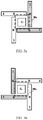
- FIGS. 2a-2b illustrate exemplary pixel cells
- FIGS. 2c-2d illustrate another exemplary pixel cells. Note that the pixel cells respectively illustrated in FIGS. 2a-2b and FIGS. 2c-2d may at least be used to define a position relationship between individual pixels.
- the starting pixel is placed vertically.
- the starting pixel is denoted as the red pixel 1.
- the next pixel is placed by overlapping with the red pixel 1, rotating by about 90 degrees clockwise using the bottom end of the red pixel 1 as the rotation center, and moving horizontally to the left until forming a T-shaped structure with the red pixel 1.
- the pixel is denoted as the blue pixel 2.
- the left end of the blue pixel 2 corresponds to the bottom end of the red pixel 1, which is the rotation center.
- the next pixel is placed by overlapping the blue pixel 2, rotating by about 90 degrees clockwise using the left end of the blue pixel 2 as the rotation center, and moving vertically to the top until forming a T-shaped structure with the blue pixel 2.
- the pixel is denoted as the red pixel 3.
- the top end of the red pixel 3 corresponds to the left end of the blue pixel 2, which is the rotation center.
- the next pixel is placed by overlapping the red pixel 3, rotating by 90 degrees clockwise using the top end of the red pixel 3 as the rotation center, and moving horizontally to the right until forming a T-shaped structure with the red pixel 3.
- the pixel is denoted as the blue pixel 4.
- the right end of the blue pixel 4 corresponds to the top end of the red pixel 3, which is the rotation center.
- the starting pixel is placed vertically.
- the starting pixel is denoted as the red pixel 1.
- the next pixel is placed by overlapping the red pixel 1, rotating by about 90 degrees counterclockwise using the bottom end of the red pixel 1 as the rotation center, and moving vertically to the top until forming a T-shaped structure with the red pixel 1.
- the pixel is denoted as the blue pixel 2.
- the right end of the blue pixel 2 corresponds to the bottom end of the red pixel 1, which is the rotation center.
- the next pixel is placed by overlapping the blue pixel 2, rotating by about 90 degrees counterclockwise using the right end of the blue pixel 2 as the rotation center, and moving horizontally to the left until forming a T-shaped structure with the blue pixel 2.
- the pixel is denoted as the red pixel 3.
- the top end of the red pixel 3 corresponds to the right end of the blue pixel 2, which is the rotation center.
- the next pixel is placed by overlapping the red pixel 3, rotating by 90 degrees counterclockwise using the top end of the red pixel 3 as the rotation center, and moving vertically to the bottom until forming a T-shaped structure with the red pixel 3.
- the pixel is denoted as the blue pixel 4.
- the left end of the blue pixel 4 corresponds to the top end of the red pixel 3, which is the rotation center.
- portions of two red (R) pixels and two blue (B) pixels may define a virtual rectangular area.
- a green (G) pixel is placed within each virtual rectangular area to form the exemplary pixel cells.
- FIGS. 2c-2d illustrate additional exemplary pixel cells.
- the starting pixel is placed horizontally.
- the starting pixel is denoted as the blue pixel 1.
- the next pixel is placed by overlapping the blue pixel 1, rotating by about 90 degrees clockwise using the left end of the blue pixel 1 as the rotation center, and moving horizontally to the right until forming a T-shaped structure with the blue pixel 1.
- the pixel is denoted as the red pixel 2.
- the top end of the red pixel 2 corresponds to the left end of the blue pixel 1, which is the rotation center.
- the next pixel is placed by overlapping the red pixel 2, rotating by about 90 degrees clockwise using the top end of the red pixel 2 as the rotation center, and moving vertically to the bottom until forming a T-shaped structure with the red pixel 2.
- the pixel is denoted as the blue pixel 3.
- the right end of the blue pixel 3 corresponds to the top end of the red pixel 2, which is the previous rotation center.
- the next pixel is placed by overlapping the blue pixel 3, rotating by about 90 degrees clockwise using the right end of the blue pixel 3 as the rotation center, and moving horizontally to the left until forming a T-shaped structure with the blue pixel 3.
- the pixel is denoted as the red pixel 4.
- the bottom end of the red pixel 4 corresponds to the right end of the blue pixel 3, which is the rotation center.
- the starting pixel is placed horizontally.
- the starting pixel is denoted as the blue pixel 1.
- the next pixel is placed by overlapping the blue pixel 1, rotating by about 90 degrees counterclockwise using the left end of the blue pixel 1 as the rotation center, and moving vertically to the bottom until forming a T-shaped structure with the blue pixel 1.
- the pixel is denoted as the red pixel 2.
- the bottom end of the red pixel 2 corresponds to the left end of the blue pixel 1, which is the rotation center.
- the next pixel is placed by overlapping the red pixel 2, rotating by 90 degrees counterclockwise using the bottom end of the red pixel 2 as the rotation center, and moving horizontally to the right until forming a T-shaped structure with the red pixel 2.
- the pixel is denoted as the blue pixel 3.
- the right end of the blue pixel 3 corresponds to the bottom end of the red pixel 2, which is the rotation center.
- the next pixel is placed by overlapping the blue pixel 3, rotating by 90 degrees counterclockwise using the right end of the blue pixel 3 as the rotation center, and moving vertically to the top until forming a T-shaped structure with the blue pixel 3.
- the pixel is denoted as the red pixel 4.
- the top end of the red pixel 4 corresponds to the right end of the blue pixel 3, which is the rotation center.
- a virtual rectangular area 20a-20d may include at least a portion of each of the separated two red (R) pixels 3, 4 and two blue (B) pixels 1, 2 configured along a side direction of the virtual rectangular area.
- the green (G) pixel is placed inside each virtual rectangular area to form exemplary pixel cells. In one embodiment, the virtual rectangular area 20a-20d is centered by the exemplary green (G) pixel.
- similar pixel cells compared with the pixel cells shown in FIGS. 2a-2d , may be formed such that pixels of the same color are perpendicular to one another and the pixels of different colors are in parallel with one another.
- FIGS. 3c-3d two red (R) pixels 3, 4 and two blue (B) pixels 1, 2 are separated from one another.
- a virtual rectangular area 30a-30d may be defined to include at least a portion of each of the separated two red (R) pixels 3, 4 and two blue (B) pixels 1, 2 configured along a side direction of the virtual rectangular area.
- the green (G) pixel is placed inside each virtual rectangular area to form exemplary pixel cells.
- the exemplary green (G) pixel is configured in the center of each of the virtual rectangular areas 30a-30d.
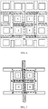
- FIG. 4 illustrates an exemplary pixel structure including exemplary pixel cells as shown in FIGS. 2a-2d .
- Two second pixels are symmetrically arranged with respect to the center of each first pixel.
- two third pixels are symmetrically arranged with respect to the center of each first pixel.
- the third pixels are perpendicular to each of the adjacent second pixels.
- the pixel structure may include the pixel cells shown in FIGS. 2a-2d .
- the pixel cells shown in FIGS. 2a-2b are labeled as type 1 pixel cells in FIG. 4 and the pixel cells shown in FIGS. 2c-2d are labeled as type 2 pixel cells in FIG. 4 .
- the type 1 and type 2 pixel cells are symmetrically configured in the vertical direction.
- FIG. 4 shows four pixel cells for illustration purposes, more or less than four pixel cells, selected from type 1 pixel cells as illustrated in FIGS. 2a-2b and type 2 pixel cells as illustrated in FIGS. 2c-2d , may be included in the pixel structure in the present disclosure.
- the pixel structure in FIG. 4 may include two type 1 pixel cells and two type 2 pixel cells. In certain embodiments, the number of pixel cells of each type may be determined by the required dimensions of the display panel.
- FIG. 5 illustrates an extended pixel structure according to FIG. 4 .
- the type 1 and type 2 pixel cells are replicated alternately in the horizontal direction and in the vertical direction. In other words, the type 1 and type 2 pixel cells appear alternately in the horizontal direction and in the vertical direction.
- adjacent pixel cells share adjacent pixels to provide pixel structure in FIGS. 4-5 .
- FIG. 6 illustrates a display area with pixel structures arranged according to FIG. 4 .
- commonly adjacent pixels are shared in any group including four adjacent pixel cells in the 2x2 arrangement, including two type 1 pixel cells and two type 2 pixel cells. It should be noted that pixels in the peripheral may be independently arranged and may not be shared.
- FIG. 7 illustrates another exemplary pixel structure with pixel cells as illustrated in FIGS. 3a-3d .
- Two adjacent second pixels are perpendicular to one another.
- Two adjacent third pixels are perpendicular to one another.
- Each second pixel is perpendicular to an adjacent third pixel.
- the pixel structure may include the pixel cells illustrated in FIGS. 3a-3d .
- the pixel cell as shown in FIG. 3a is labeled as type 1 pixel cell in FIG. 7 .
- the pixel cell as shown in FIG. 3b is labeled as type 2 pixel cell in FIG. 7 .
- the pixel cell as shown in FIG. 3c is labeled as type 3 pixel cell in FIG. 7 .
- the pixel cell as shown in FIG. 3d is labeled as type 4 pixel cell in FIG. 7 .
- the type 1 and type 2 pixel cells are symmetrically configured in the vertical direction.
- the type 1 and type 3 pixel cells are symmetrically configured in the horizontal direction.
- the type 2 and type 4 pixel cells are symmetrically configured in the horizontal direction.
- the type 3 and type 4 pixel cells are symmetrically configured in the vertical direction.
- FIG. 7 shows four pixel cells for illustration purposes, more or less than four pixel cells, selected from type 1 pixel cell as illustrated in FIG. 3a , type 2 pixel cell as illustrated in FIG. 3b , type 3 pixel cell as illustrated in FIG. 3c , and type 4 pixel cell as illustrated in FIG. 3d , may be included in the pixel structure in the present disclosure.
- the number of pixel cells of each type may be determined by the required dimensions of the display panel.
- FIG. 8 illustrates an extended pixel structure according to FIG. 7 .
- Each exemplary pixel structure in FIG. 7 may include the four types of pixel cells in FIGS. 3a-3d .
- the type 1, type 2, type 3 and type 4 pixel cells are replicated alternately in the horizontal direction and in the vertical direction. In other words, the type 1, type 2, type 3 and type 4 pixel cells appear alternately in the horizontal direction and in the vertical direction.
- adjacent pixel cells may share adjacent pixels to provide the exemplary pixel structures in FIGS. 7-8 .
- FIG. 9 illustrates a display area with pixel structures arranged according to FIG. 7 .
- commonly adjacent pixels are shared in any group including four adjacent pixel cells shown in FIGS. 3a-3d in the exemplary 2x2 arrangement.
- pixels in the peripheral may be independently arranged and may not be shared.
- individual pixels may be separated by a predetermined distance.
- the number of green (G) pixels may be equal to the number of pixel cells.
- the number of red (R) pixels and the number of blue (B) pixels may be the same, which is equal to a half of the number of pixel cells.
- each pixel cell in a pixel structure may include one first pixel, one quarter of the two second pixels, and one quarter of the two third pixels.
- the present disclosure reduces the number of pixels required for each pixel cell, and reduces the physical density of pixels while the pixel resolution of image display remains the same.
- the process complexity and production cost are reduced and the production yield is increased, for example, for producing high resolution display products such as thin film transistor liquid crystal display (TFT LCD) and active-matrix organic light-emitting diode (AMOLD) displays.
- TFT LCD thin film transistor liquid crystal display
- AMOLD active-matrix organic light-emitting diode
- the present disclosure also provides a display panel.
- the display panel may include pixel cells in FIGS. 2a-2d and FIGS. 3a-3d arranged according to the disclosed methods. The detail description will not be duplicated herein.
- the disclosed display panel may include a TFT LCD or an OLED display panel, or any other suitable display panel.
- a TFT LCD display panel may include an array substrate and a color filter substrate.
- An OLED display panel may include an array substrate.
- the present disclosure also provides a display apparatus.
- the display apparatus may include a disclosed display panel.
- the disclosed display apparatus may be a color liquid crystal display (LCD) display apparatus, an organic light-emitting diode (OLED) display apparatus, a cathode ray tube (CRT) display apparatus, a plasma apparatus, an electronic paper display apparatus, an AMOLED display apparatus, or any suitable display apparatus, without limitation.
- LCD liquid crystal display
- OLED organic light-emitting diode
- CRT cathode ray tube
- plasma apparatus an electronic paper display apparatus
- AMOLED display apparatus any suitable display apparatus, without limitation.
Landscapes
- Engineering & Computer Science (AREA)
- Physics & Mathematics (AREA)
- Computer Hardware Design (AREA)
- General Physics & Mathematics (AREA)
- Theoretical Computer Science (AREA)
- Electroluminescent Light Sources (AREA)
- Devices For Indicating Variable Information By Combining Individual Elements (AREA)
Claims (13)
- Pixelstruktur, aufweisend:
mehrere Pixelzellen mit einer ersten Pixelzelle und benachbarten Pixelzellen, wobei jede Pixelzelle Folgendes aufweist:ein erstes Pixel (G); undzwei zweite Pixel (R,R; R,B) und zwei dritte Pixel (B,B; B,R), die das erste Pixel (G) umgeben und ihm benachbart sind, und wobei zwei der zwei zweiten Pixel (R,R; R,B) und die zwei dritten Pixel auf zwei gegenüberliegenden Seiten des ersten Pixels (G) angeordnet sind, wobei die anderen zwei der beiden zweiten Pixel und die zwei dritten Pixel (B,B; B,R) an den zwei gegenüberliegenden übrigen Seiten des ersten Pixels (G) angeordnet sind,jedes der beiden zweiten Pixel (R,R; R,B) und der dritten Pixel (B,B; B,R) eine rechteckige Gestalt mit einer Längsrichtung aufweist,dadurch gekennzeichnet, dassjedes der beiden zweiten Pixel (R,R; R,B) auch ein zweites Pixel einer benachbarten zweiten Pixelzelle ist, die der ersten Pixelzelle benachbart ist, die entlang der Längsrichtung der zweiten Pixel (R,R; R,B) angeordnet ist, und das zweite Pixel auch ein zweites Pixel von benachbarten dritten und vierten Pixelzellen ist, die ersten und zweiten Pixelzellen einerseits und die dritten und vierten Pixelzellen andererseits jeweils symmetrisch in Bezug auf eine Achse senkrecht zu der Längsrichtung des zweiten Pixels sind, jedes der beiden dritten Pixel (B,B; B,R) auch ein drittes Pixel einer benachbarten fünften Pixelzelle ist, die der ersten Pixelzelle benachbart ist, die entlang der Längsrichtung der dritten Pixel (B,B; B,R) angeordnet ist, und das dritte Pixel auch ein drittes Pixel von benachbarten sechsten und siebten Pixelzellen ist, die ersten und fünften Pixelzellen einerseits und die sechsten und siebten Pixelzellen andererseits jeweils symmetrisch in Bezug auf eine Achse sind, die senkrecht zu der Längsrichtung des dritten Pixels ist. - Pixelstruktur nach Anspruch 1, wobei:
jedes zweite Pixel (R,R; R,B) senkrecht zu jedem der dritten Pixel (B,B; B,R) ist, das dem zweiten Pixel (R,R; R,B) benachbart ist. - Pixelstruktur nach Anspruch 2, wobei:
das zweite Pixel (R,R; R,B) und jedes der benachbarten dritten Pixel (B,B; B,R) so angeordnet sind, dass sie eine T-Gestalt bilden, wobei ein Pixel mit einer Mitte des anderen Pixels entlang seiner Längsachse ausgerichtet ist. - Pixelstruktur nach Anspruch 1, wobei:das erste Pixel (G) eine rechteckige Gestalt hat, unddie ersten Pixel (G) in den mehreren Pixelzellen einheitlich konfiguriert sind;vorzugsweise das erste Pixel (G) eine quadratische Gestalt hat.
- Pixelstruktur nach Anspruch 4, wobei:das erste Pixel (G) eine quadratische Gestalt hat,die beiden zweiten Pixel (R,R; R,B) und die beiden dritten Pixel (B,B; B,R) im Wesentlichen die gleiche Länge haben, unddie gleiche Länge größer ist als das Doppelte einer Länge des ersten Pixels (G);vorzugsweise die gleiche Länge im Wesentlichen das Doppelte einer Länge des ersten Pixels (G) plus einer Breite des zweiten Pixels (R,R; R,B) oder des dritten Pixels (B,B; B,R) beträgt.
- Pixelstruktur nach Anspruch 5, wobei jedes von dem ersten Pixel, den beiden zweiten Pixeln (R,R; R,B) und den beiden dritten Pixeln (B,B; B,R) eine abgeschrägte Ecke aufweist; vorzugsweise das benachbarte zweite Pixel (R,R; R,B) und das dritte Pixel (B,B; B,R) so angeordnet sind, dass sie eine T-Gestalt bilden, wobei ein Pixel mit einer Mitte des anderen Pixels entlang seiner Längsachse ausgerichtet ist.
- Pixelstruktur nach Anspruch 6, wobei gleiche Pixel aus den zwei zweiten Pixeln (R,R; R,B) und den zwei dritten Pixeln (B,B; B,R) in jeder Pixelzelle auf gegenüberliegenden Seiten des ersten Pixels angeordnet sind.
- Pixelstruktur nach Anspruch 6, wobei
unterschiedliche Pixel aus den zwei zweiten Pixeln (R,R; R,B) und den zwei dritten Pixeln (B,B; B,R) in jeder Pixelzelle auf gegenüberliegenden Seiten des ersten Pixels (G) konfiguriert sind. - Pixelstruktur nach einem der Ansprüche 1 - 8, wobei:das erste Pixel (G), das zweite Pixel (R,R; R,B) und das dritte Pixel (B,B; B,R) konfiguriert sind, um Lichter unterschiedlicher Farbe zu emittieren;vorzugsweise:das erste Pixel (G) konfiguriert ist, um grünes Licht zu emittieren,das zweite Pixel (R,R; R,B) konfiguriert ist, um entweder rotes oder blaues Licht zu emittieren, unddas dritte Pixel (B,B; B,R) konfiguriert ist, um entweder rotes oder blaues Licht zu emittieren.
- Pixelstruktur nach Anspruch 7, wobei die gleichen Pixel symmetrisch angeordnet und durch das erste Pixel (G) zentriert sind.
- Pixelstruktur nach Anspruch 8, wobei die unterschiedlichen Pixel symmetrisch angeordnet und durch das erste Pixel (G) zentriert sind.
- Anzeigetafel, die Pixelstruktur nach einem der Ansprüche 1 bis 11 aufweisend.
- Anzeigevorrichtung, die Anzeigetafel nach Anspruch 12 aufweisend.
Applications Claiming Priority (2)
| Application Number | Priority Date | Filing Date | Title |
|---|---|---|---|
| CN201510197247.1A CN104766563B (zh) | 2015-04-23 | 2015-04-23 | 一种像素结构及显示面板和显示装置 |
| PCT/CN2015/097047 WO2016169278A1 (en) | 2015-04-23 | 2015-12-10 | Pixel structure, display panel, and display apparatus |
Publications (3)
| Publication Number | Publication Date |
|---|---|
| EP3286751A1 EP3286751A1 (de) | 2018-02-28 |
| EP3286751A4 EP3286751A4 (de) | 2018-11-21 |
| EP3286751B1 true EP3286751B1 (de) | 2022-08-17 |
Family
ID=53648353
Family Applications (1)
| Application Number | Title | Priority Date | Filing Date |
|---|---|---|---|
| EP15849826.1A Active EP3286751B1 (de) | 2015-04-23 | 2015-12-10 | Pixelstruktur, anzeigetafel und anzeigevorrichtung |
Country Status (4)
| Country | Link |
|---|---|
| US (1) | US9935155B2 (de) |
| EP (1) | EP3286751B1 (de) |
| CN (1) | CN104766563B (de) |
| WO (1) | WO2016169278A1 (de) |
Families Citing this family (14)
| Publication number | Priority date | Publication date | Assignee | Title |
|---|---|---|---|---|
| CN104766563B (zh) | 2015-04-23 | 2016-03-02 | 京东方科技集团股份有限公司 | 一种像素结构及显示面板和显示装置 |
| CN105096911B (zh) * | 2015-08-28 | 2018-10-30 | 厦门天马微电子有限公司 | 像素结构、包含其的阵列基板和显示装置 |
| CN106486513B (zh) * | 2015-08-31 | 2023-09-29 | 昆山国显光电有限公司 | 像素结构以及oled显示面板 |
| US11430411B2 (en) * | 2015-11-26 | 2022-08-30 | Barco Nv | Content sharing protocol |
| CN108511481B (zh) * | 2017-08-31 | 2019-07-26 | 昆山国显光电有限公司 | 像素结构及显示装置 |
| WO2019042013A1 (zh) | 2017-08-31 | 2019-03-07 | 昆山国显光电有限公司 | 像素结构及显示装置 |
| US11423812B2 (en) | 2017-12-14 | 2022-08-23 | Hewlett-Packard Development Company, L.P. | Rotatable substrates having micro-light emitting diodes (LEDs) |
| CN113851513A (zh) * | 2018-01-02 | 2021-12-28 | 京东方科技集团股份有限公司 | 一种显示基板、高精度金属掩模板组及显示装置 |
| KR102623201B1 (ko) * | 2018-11-29 | 2024-01-09 | 엘지디스플레이 주식회사 | 전계발광 표시장치 |
| KR102866754B1 (ko) | 2019-03-04 | 2025-09-30 | 삼성디스플레이 주식회사 | 표시 장치, 표시 장치의 제조장치 및 표시 장치의 제조방법 |
| US11557635B2 (en) | 2019-12-10 | 2023-01-17 | Samsung Display Co., Ltd. | Display device, mask assembly, and apparatus for manufacturing the display device |
| US12419175B2 (en) | 2019-12-10 | 2025-09-16 | Samsung Display Co., Ltd. | Display device, mask assembly, and apparatus for manufacturing display device |
| CN120569022A (zh) * | 2020-10-23 | 2025-08-29 | 武汉天马微电子有限公司 | 一种显示面板及显示装置 |
| CN113035125A (zh) * | 2021-03-09 | 2021-06-25 | 京东方科技集团股份有限公司 | 一种显示面板、显示装置及其控制方法 |
Family Cites Families (13)
| Publication number | Priority date | Publication date | Assignee | Title |
|---|---|---|---|---|
| US7508431B2 (en) | 2004-06-17 | 2009-03-24 | Hoya Corporation | Solid state imaging device |
| US9041625B2 (en) | 2010-04-21 | 2015-05-26 | Lg Display Co., Ltd. | Subpixel arrangement structure for a display device and display device |
| KR101189025B1 (ko) * | 2010-05-31 | 2012-10-08 | 삼성디스플레이 주식회사 | 유기전계발광 표시장치의 화소배열구조 |
| US8902245B2 (en) * | 2011-04-07 | 2014-12-02 | Universal Display Corporation | Method for driving quad-subpixel display |
| US8552420B2 (en) * | 2011-08-09 | 2013-10-08 | Universal Display Corporation | OLED light panel with controlled brightness variation |
| US8921842B2 (en) * | 2012-11-14 | 2014-12-30 | Lg Display Co., Ltd. | Organic light emitting display device and method of manufacturing the same |
| CN103024305B (zh) | 2012-12-27 | 2018-05-29 | 上海集成电路研发中心有限公司 | 改进的像素阵列 |
| KR102030799B1 (ko) | 2013-03-11 | 2019-10-11 | 삼성디스플레이 주식회사 | 유기발광표시장치 |
| CN103366683B (zh) | 2013-07-12 | 2014-10-29 | 上海和辉光电有限公司 | 像素阵列、显示器以及将图像呈现于显示器上的方法 |
| KR102124043B1 (ko) | 2013-07-25 | 2020-06-18 | 삼성디스플레이 주식회사 | 화소 배열 구조 및 이를 채용하는 표시 장치 |
| US9262961B2 (en) * | 2013-08-30 | 2016-02-16 | Au Optronics Corporation | Pixel arrangement of color display apparatus |
| CN104464541B (zh) * | 2014-12-30 | 2017-10-17 | 昆山国显光电有限公司 | 显示屏及其驱动方法 |
| CN104766563B (zh) | 2015-04-23 | 2016-03-02 | 京东方科技集团股份有限公司 | 一种像素结构及显示面板和显示装置 |
-
2015
- 2015-04-23 CN CN201510197247.1A patent/CN104766563B/zh active Active
- 2015-12-10 US US15/031,026 patent/US9935155B2/en active Active
- 2015-12-10 EP EP15849826.1A patent/EP3286751B1/de active Active
- 2015-12-10 WO PCT/CN2015/097047 patent/WO2016169278A1/en not_active Ceased
Also Published As
| Publication number | Publication date |
|---|---|
| US20170104040A1 (en) | 2017-04-13 |
| EP3286751A1 (de) | 2018-02-28 |
| CN104766563B (zh) | 2016-03-02 |
| US9935155B2 (en) | 2018-04-03 |
| EP3286751A4 (de) | 2018-11-21 |
| CN104766563A (zh) | 2015-07-08 |
| WO2016169278A1 (en) | 2016-10-27 |
Similar Documents
| Publication | Publication Date | Title |
|---|---|---|
| EP3286751B1 (de) | Pixelstruktur, anzeigetafel und anzeigevorrichtung | |
| JP7633334B2 (ja) | 画素配列構造、表示パネル及び表示装置 | |
| KR101755271B1 (ko) | 화소 배열 구조, 표시 패널 및 표시 장치 | |
| EP3203523B1 (de) | Anzeigeverfahren für eine pixelstruktur | |
| CN109713027B (zh) | 一种有机发光显示面板的像素排布及有机发光显示面板 | |
| US9735207B2 (en) | Display substrate and driving method thereof, display apparatus | |
| US9542885B2 (en) | Pixel unit, display panel, display method and display device | |
| US10013938B2 (en) | Display panel and display device, and fabrication method thereof | |
| CN103472608B (zh) | 显示面板的像素与子像素配置 | |
| EP3281227B1 (de) | Pixelstruktur, anzeigetafel und anzeigevorrichtung | |
| EP3121804B1 (de) | Pixelstruktur, anzeigesubstrat und anzeigevorrichtung | |
| US9779645B2 (en) | Display panel, display method and display device | |
| WO2019041910A1 (zh) | 显示面板以及显示装置 | |
| US20150380471A1 (en) | Pixel arrangement structure, display device and display method thereof | |
| US9892696B2 (en) | Display panel having a plurality of pixels driven in a time-sharing manner, display method thereof and display device | |
| US20160223856A1 (en) | Display substrate and display apparatus | |
| CN110320719A (zh) | 显示面板及其制作方法和显示装置 | |
| CN105355643B (zh) | 一种像素结构、其制作方法、显示面板及显示装置 | |
| US9472143B2 (en) | Pixel structure and driving method thereof, display panel and display device | |
| CN107799013B (zh) | 一种显示面板、显示屏及显示装置 | |
| WO2020073401A1 (zh) | 像素结构、阵列基板及显示装置 | |
| CN106782097A (zh) | 一种显示基板、显示面板以及显示装置 | |
| CN109581723B (zh) | 一种显示面板和显示装置 | |
| CN105044954A (zh) | 像素结构、显示方法及显示面板 | |
| JP2005315960A (ja) | カラー画像表示装置 |
Legal Events
| Date | Code | Title | Description |
|---|---|---|---|
| STAA | Information on the status of an ep patent application or granted ep patent |
Free format text: STATUS: THE INTERNATIONAL PUBLICATION HAS BEEN MADE |
|
| PUAI | Public reference made under article 153(3) epc to a published international application that has entered the european phase |
Free format text: ORIGINAL CODE: 0009012 |
|
| STAA | Information on the status of an ep patent application or granted ep patent |
Free format text: STATUS: REQUEST FOR EXAMINATION WAS MADE |
|
| 17P | Request for examination filed |
Effective date: 20160421 |
|
| AK | Designated contracting states |
Kind code of ref document: A1 Designated state(s): AL AT BE BG CH CY CZ DE DK EE ES FI FR GB GR HR HU IE IS IT LI LT LU LV MC MK MT NL NO PL PT RO RS SE SI SK SM TR |
|
| AX | Request for extension of the european patent |
Extension state: BA ME |
|
| DAV | Request for validation of the european patent (deleted) | ||
| DAX | Request for extension of the european patent (deleted) | ||
| REG | Reference to a national code |
Ref country code: DE Ref legal event code: R079 Ref document number: 602015080410 Country of ref document: DE Free format text: PREVIOUS MAIN CLASS: G09G0003200000 Ipc: H01L0027320000 |
|
| A4 | Supplementary search report drawn up and despatched |
Effective date: 20181018 |
|
| RIC1 | Information provided on ipc code assigned before grant |
Ipc: H01L 27/32 20060101AFI20181012BHEP Ipc: G09G 3/20 20060101ALI20181012BHEP |
|
| STAA | Information on the status of an ep patent application or granted ep patent |
Free format text: STATUS: EXAMINATION IS IN PROGRESS |
|
| 17Q | First examination report despatched |
Effective date: 20200529 |
|
| GRAP | Despatch of communication of intention to grant a patent |
Free format text: ORIGINAL CODE: EPIDOSNIGR1 |
|
| STAA | Information on the status of an ep patent application or granted ep patent |
Free format text: STATUS: GRANT OF PATENT IS INTENDED |
|
| INTG | Intention to grant announced |
Effective date: 20220506 |
|
| GRAS | Grant fee paid |
Free format text: ORIGINAL CODE: EPIDOSNIGR3 |
|
| GRAA | (expected) grant |
Free format text: ORIGINAL CODE: 0009210 |
|
| STAA | Information on the status of an ep patent application or granted ep patent |
Free format text: STATUS: THE PATENT HAS BEEN GRANTED |
|
| AK | Designated contracting states |
Kind code of ref document: B1 Designated state(s): AL AT BE BG CH CY CZ DE DK EE ES FI FR GB GR HR HU IE IS IT LI LT LU LV MC MK MT NL NO PL PT RO RS SE SI SK SM TR |
|
| REG | Reference to a national code |
Ref country code: CH Ref legal event code: EP |
|
| REG | Reference to a national code |
Ref country code: DE Ref legal event code: R096 Ref document number: 602015080410 Country of ref document: DE |
|
| REG | Reference to a national code |
Ref country code: IE Ref legal event code: FG4D |
|
| REG | Reference to a national code |
Ref country code: AT Ref legal event code: REF Ref document number: 1512734 Country of ref document: AT Kind code of ref document: T Effective date: 20220915 |
|
| REG | Reference to a national code |
Ref country code: DE Ref legal event code: R079 Ref document number: 602015080410 Country of ref document: DE Free format text: PREVIOUS MAIN CLASS: H01L0027320000 Ipc: H10K0059000000 |
|
| REG | Reference to a national code |
Ref country code: NL Ref legal event code: MP Effective date: 20220817 |
|
| REG | Reference to a national code |
Ref country code: LT Ref legal event code: MG9D |
|
| PG25 | Lapsed in a contracting state [announced via postgrant information from national office to epo] |
Ref country code: SE Free format text: LAPSE BECAUSE OF FAILURE TO SUBMIT A TRANSLATION OF THE DESCRIPTION OR TO PAY THE FEE WITHIN THE PRESCRIBED TIME-LIMIT Effective date: 20220817 Ref country code: RS Free format text: LAPSE BECAUSE OF FAILURE TO SUBMIT A TRANSLATION OF THE DESCRIPTION OR TO PAY THE FEE WITHIN THE PRESCRIBED TIME-LIMIT Effective date: 20220817 Ref country code: PT Free format text: LAPSE BECAUSE OF FAILURE TO SUBMIT A TRANSLATION OF THE DESCRIPTION OR TO PAY THE FEE WITHIN THE PRESCRIBED TIME-LIMIT Effective date: 20221219 Ref country code: NO Free format text: LAPSE BECAUSE OF FAILURE TO SUBMIT A TRANSLATION OF THE DESCRIPTION OR TO PAY THE FEE WITHIN THE PRESCRIBED TIME-LIMIT Effective date: 20221117 Ref country code: NL Free format text: LAPSE BECAUSE OF FAILURE TO SUBMIT A TRANSLATION OF THE DESCRIPTION OR TO PAY THE FEE WITHIN THE PRESCRIBED TIME-LIMIT Effective date: 20220817 Ref country code: LV Free format text: LAPSE BECAUSE OF FAILURE TO SUBMIT A TRANSLATION OF THE DESCRIPTION OR TO PAY THE FEE WITHIN THE PRESCRIBED TIME-LIMIT Effective date: 20220817 Ref country code: LT Free format text: LAPSE BECAUSE OF FAILURE TO SUBMIT A TRANSLATION OF THE DESCRIPTION OR TO PAY THE FEE WITHIN THE PRESCRIBED TIME-LIMIT Effective date: 20220817 Ref country code: FI Free format text: LAPSE BECAUSE OF FAILURE TO SUBMIT A TRANSLATION OF THE DESCRIPTION OR TO PAY THE FEE WITHIN THE PRESCRIBED TIME-LIMIT Effective date: 20220817 Ref country code: ES Free format text: LAPSE BECAUSE OF FAILURE TO SUBMIT A TRANSLATION OF THE DESCRIPTION OR TO PAY THE FEE WITHIN THE PRESCRIBED TIME-LIMIT Effective date: 20220817 |
|
| REG | Reference to a national code |
Ref country code: AT Ref legal event code: MK05 Ref document number: 1512734 Country of ref document: AT Kind code of ref document: T Effective date: 20220817 |
|
| PG25 | Lapsed in a contracting state [announced via postgrant information from national office to epo] |
Ref country code: PL Free format text: LAPSE BECAUSE OF FAILURE TO SUBMIT A TRANSLATION OF THE DESCRIPTION OR TO PAY THE FEE WITHIN THE PRESCRIBED TIME-LIMIT Effective date: 20220817 Ref country code: IS Free format text: LAPSE BECAUSE OF FAILURE TO SUBMIT A TRANSLATION OF THE DESCRIPTION OR TO PAY THE FEE WITHIN THE PRESCRIBED TIME-LIMIT Effective date: 20221217 Ref country code: HR Free format text: LAPSE BECAUSE OF FAILURE TO SUBMIT A TRANSLATION OF THE DESCRIPTION OR TO PAY THE FEE WITHIN THE PRESCRIBED TIME-LIMIT Effective date: 20220817 Ref country code: GR Free format text: LAPSE BECAUSE OF FAILURE TO SUBMIT A TRANSLATION OF THE DESCRIPTION OR TO PAY THE FEE WITHIN THE PRESCRIBED TIME-LIMIT Effective date: 20221118 |
|
| PG25 | Lapsed in a contracting state [announced via postgrant information from national office to epo] |
Ref country code: SM Free format text: LAPSE BECAUSE OF FAILURE TO SUBMIT A TRANSLATION OF THE DESCRIPTION OR TO PAY THE FEE WITHIN THE PRESCRIBED TIME-LIMIT Effective date: 20220817 Ref country code: RO Free format text: LAPSE BECAUSE OF FAILURE TO SUBMIT A TRANSLATION OF THE DESCRIPTION OR TO PAY THE FEE WITHIN THE PRESCRIBED TIME-LIMIT Effective date: 20220817 Ref country code: DK Free format text: LAPSE BECAUSE OF FAILURE TO SUBMIT A TRANSLATION OF THE DESCRIPTION OR TO PAY THE FEE WITHIN THE PRESCRIBED TIME-LIMIT Effective date: 20220817 Ref country code: CZ Free format text: LAPSE BECAUSE OF FAILURE TO SUBMIT A TRANSLATION OF THE DESCRIPTION OR TO PAY THE FEE WITHIN THE PRESCRIBED TIME-LIMIT Effective date: 20220817 Ref country code: AT Free format text: LAPSE BECAUSE OF FAILURE TO SUBMIT A TRANSLATION OF THE DESCRIPTION OR TO PAY THE FEE WITHIN THE PRESCRIBED TIME-LIMIT Effective date: 20220817 |
|
| REG | Reference to a national code |
Ref country code: DE Ref legal event code: R097 Ref document number: 602015080410 Country of ref document: DE |
|
| PG25 | Lapsed in a contracting state [announced via postgrant information from national office to epo] |
Ref country code: SK Free format text: LAPSE BECAUSE OF FAILURE TO SUBMIT A TRANSLATION OF THE DESCRIPTION OR TO PAY THE FEE WITHIN THE PRESCRIBED TIME-LIMIT Effective date: 20220817 Ref country code: EE Free format text: LAPSE BECAUSE OF FAILURE TO SUBMIT A TRANSLATION OF THE DESCRIPTION OR TO PAY THE FEE WITHIN THE PRESCRIBED TIME-LIMIT Effective date: 20220817 |
|
| PLBE | No opposition filed within time limit |
Free format text: ORIGINAL CODE: 0009261 |
|
| STAA | Information on the status of an ep patent application or granted ep patent |
Free format text: STATUS: NO OPPOSITION FILED WITHIN TIME LIMIT |
|
| PG25 | Lapsed in a contracting state [announced via postgrant information from national office to epo] |
Ref country code: AL Free format text: LAPSE BECAUSE OF FAILURE TO SUBMIT A TRANSLATION OF THE DESCRIPTION OR TO PAY THE FEE WITHIN THE PRESCRIBED TIME-LIMIT Effective date: 20220817 |
|
| 26N | No opposition filed |
Effective date: 20230519 |
|
| REG | Reference to a national code |
Ref country code: CH Ref legal event code: PL |
|
| GBPC | Gb: european patent ceased through non-payment of renewal fee |
Effective date: 20221210 |
|
| REG | Reference to a national code |
Ref country code: BE Ref legal event code: MM Effective date: 20221231 |
|
| PG25 | Lapsed in a contracting state [announced via postgrant information from national office to epo] |
Ref country code: SI Free format text: LAPSE BECAUSE OF FAILURE TO SUBMIT A TRANSLATION OF THE DESCRIPTION OR TO PAY THE FEE WITHIN THE PRESCRIBED TIME-LIMIT Effective date: 20220817 Ref country code: LU Free format text: LAPSE BECAUSE OF NON-PAYMENT OF DUE FEES Effective date: 20221210 |
|
| PG25 | Lapsed in a contracting state [announced via postgrant information from national office to epo] |
Ref country code: LI Free format text: LAPSE BECAUSE OF NON-PAYMENT OF DUE FEES Effective date: 20221231 Ref country code: IE Free format text: LAPSE BECAUSE OF NON-PAYMENT OF DUE FEES Effective date: 20221210 Ref country code: GB Free format text: LAPSE BECAUSE OF NON-PAYMENT OF DUE FEES Effective date: 20221210 Ref country code: CH Free format text: LAPSE BECAUSE OF NON-PAYMENT OF DUE FEES Effective date: 20221231 |
|
| PG25 | Lapsed in a contracting state [announced via postgrant information from national office to epo] |
Ref country code: FR Free format text: LAPSE BECAUSE OF NON-PAYMENT OF DUE FEES Effective date: 20221231 Ref country code: BE Free format text: LAPSE BECAUSE OF NON-PAYMENT OF DUE FEES Effective date: 20221231 |
|
| PG25 | Lapsed in a contracting state [announced via postgrant information from national office to epo] |
Ref country code: HU Free format text: LAPSE BECAUSE OF FAILURE TO SUBMIT A TRANSLATION OF THE DESCRIPTION OR TO PAY THE FEE WITHIN THE PRESCRIBED TIME-LIMIT; INVALID AB INITIO Effective date: 20151210 |
|
| PG25 | Lapsed in a contracting state [announced via postgrant information from national office to epo] |
Ref country code: CY Free format text: LAPSE BECAUSE OF FAILURE TO SUBMIT A TRANSLATION OF THE DESCRIPTION OR TO PAY THE FEE WITHIN THE PRESCRIBED TIME-LIMIT Effective date: 20220817 |
|
| PG25 | Lapsed in a contracting state [announced via postgrant information from national office to epo] |
Ref country code: MK Free format text: LAPSE BECAUSE OF FAILURE TO SUBMIT A TRANSLATION OF THE DESCRIPTION OR TO PAY THE FEE WITHIN THE PRESCRIBED TIME-LIMIT Effective date: 20220817 Ref country code: IT Free format text: LAPSE BECAUSE OF FAILURE TO SUBMIT A TRANSLATION OF THE DESCRIPTION OR TO PAY THE FEE WITHIN THE PRESCRIBED TIME-LIMIT Effective date: 20220817 |
|
| PG25 | Lapsed in a contracting state [announced via postgrant information from national office to epo] |
Ref country code: MC Free format text: LAPSE BECAUSE OF FAILURE TO SUBMIT A TRANSLATION OF THE DESCRIPTION OR TO PAY THE FEE WITHIN THE PRESCRIBED TIME-LIMIT Effective date: 20220817 |
|
| PG25 | Lapsed in a contracting state [announced via postgrant information from national office to epo] |
Ref country code: TR Free format text: LAPSE BECAUSE OF FAILURE TO SUBMIT A TRANSLATION OF THE DESCRIPTION OR TO PAY THE FEE WITHIN THE PRESCRIBED TIME-LIMIT Effective date: 20220817 Ref country code: MC Free format text: LAPSE BECAUSE OF FAILURE TO SUBMIT A TRANSLATION OF THE DESCRIPTION OR TO PAY THE FEE WITHIN THE PRESCRIBED TIME-LIMIT Effective date: 20220817 |
|
| PG25 | Lapsed in a contracting state [announced via postgrant information from national office to epo] |
Ref country code: BG Free format text: LAPSE BECAUSE OF FAILURE TO SUBMIT A TRANSLATION OF THE DESCRIPTION OR TO PAY THE FEE WITHIN THE PRESCRIBED TIME-LIMIT Effective date: 20220817 |
|
| PG25 | Lapsed in a contracting state [announced via postgrant information from national office to epo] |
Ref country code: MT Free format text: LAPSE BECAUSE OF FAILURE TO SUBMIT A TRANSLATION OF THE DESCRIPTION OR TO PAY THE FEE WITHIN THE PRESCRIBED TIME-LIMIT Effective date: 20220817 |
|
| PGFP | Annual fee paid to national office [announced via postgrant information from national office to epo] |
Ref country code: DE Payment date: 20251211 Year of fee payment: 11 |