EP3285386B1 - Matrixgleichstrom-wechselstromwandler - Google Patents
Matrixgleichstrom-wechselstromwandler Download PDFInfo
- Publication number
- EP3285386B1 EP3285386B1 EP17185806.1A EP17185806A EP3285386B1 EP 3285386 B1 EP3285386 B1 EP 3285386B1 EP 17185806 A EP17185806 A EP 17185806A EP 3285386 B1 EP3285386 B1 EP 3285386B1
- Authority
- EP
- European Patent Office
- Prior art keywords
- signal
- phase
- voltage
- measured values
- processing means
- Prior art date
- Legal status (The legal status is an assumption and is not a legal conclusion. Google has not performed a legal analysis and makes no representation as to the accuracy of the status listed.)
- Active
Links
Images


Classifications
-
- H—ELECTRICITY
- H02—GENERATION; CONVERSION OR DISTRIBUTION OF ELECTRIC POWER
- H02M—APPARATUS FOR CONVERSION BETWEEN AC AND AC, BETWEEN AC AND DC, OR BETWEEN DC AND DC, AND FOR USE WITH MAINS OR SIMILAR POWER SUPPLY SYSTEMS; CONVERSION OF DC OR AC INPUT POWER INTO SURGE OUTPUT POWER; CONTROL OR REGULATION THEREOF
- H02M5/00—Conversion of AC power input into AC power output, e.g. for change of voltage, for change of frequency, for change of number of phases
- H02M5/02—Conversion of AC power input into AC power output, e.g. for change of voltage, for change of frequency, for change of number of phases without intermediate conversion into DC
- H02M5/04—Conversion of AC power input into AC power output, e.g. for change of voltage, for change of frequency, for change of number of phases without intermediate conversion into DC by static converters
- H02M5/22—Conversion of AC power input into AC power output, e.g. for change of voltage, for change of frequency, for change of number of phases without intermediate conversion into DC by static converters using discharge tubes with control electrode or semiconductor devices with control electrode
- H02M5/275—Conversion of AC power input into AC power output, e.g. for change of voltage, for change of frequency, for change of number of phases without intermediate conversion into DC by static converters using discharge tubes with control electrode or semiconductor devices with control electrode using devices of a triode or transistor type requiring continuous application of a control signal
- H02M5/297—Conversion of AC power input into AC power output, e.g. for change of voltage, for change of frequency, for change of number of phases without intermediate conversion into DC by static converters using discharge tubes with control electrode or semiconductor devices with control electrode using devices of a triode or transistor type requiring continuous application of a control signal for conversion of frequency
-
- H—ELECTRICITY
- H02—GENERATION; CONVERSION OR DISTRIBUTION OF ELECTRIC POWER
- H02M—APPARATUS FOR CONVERSION BETWEEN AC AND AC, BETWEEN AC AND DC, OR BETWEEN DC AND DC, AND FOR USE WITH MAINS OR SIMILAR POWER SUPPLY SYSTEMS; CONVERSION OF DC OR AC INPUT POWER INTO SURGE OUTPUT POWER; CONTROL OR REGULATION THEREOF
- H02M1/00—Details of apparatus for conversion
- H02M1/12—Arrangements for reducing harmonics from AC input or output
- H02M1/123—Suppression of common mode voltage or current
Definitions
- the present invention relates to a matrix direct AC/AC converter.
- the present invention finds advantageous, though non-exclusive, application in the control of variable-speed three-phase AC motors, to which the ensuing description will make explicit reference, without implying any loss of generality.
- an AC/AC converter converts AC electric power at a certain frequency and a certain voltage amplitude into AC electric power at another frequency and another voltage amplitude.
- an AC/AC converter is used for converting electric power from a frequency ranging between 50 and 60 Hz to a frequency ranging or variable in a frequency range between 0 and 1200 Hz.
- the most desired characteristic of an AC/AC converter is that of generating a voltage with arbitrary amplitude and frequency for any electrical load, at the same time maintaining a unit power factor on the power-supply mains.
- a three-phase AC/AC converter is designed to be connected between the phases of a three-phase input line, for example the three-phase power mains, and the phases of a three-phase output line, for example the supply line of a three-phase AC motor.
- a matrix direct AC/AC converter typically comprises nine electronic two-way switching devices, which are arranged so as to connect, one by one, all the input phases with all the output phases, according, precisely, to the principle of a two-dimensional matrix, and a control device, that generates PWM signals for controlling accordingly the switching devices in such a way as to obtain on the output phases voltages and currents with sinusoidal waveforms.
- the European patent No. EP146032B1 describes a matrix direct AC/AC converter in which the control device generates PWM signals such as to generate, on the three-phase output line, a so-called homopolar voltage component, which does not alter the waveform of the concatenated output voltages, which are the voltages that are applied to an AC motor, but regulates the amplitude thereof with respect to a hypothetical external potential reference, which is assumed as being the centre hub of the three-phase supply voltage, i.e., the ground potential.
- the homopolar component is also known as "common-mode component” or "third-harmonic component", in so far as it has a frequency that is typically three times that of the concatenated output voltages.
- the AC/AC converter described in the patent EP146032B1 is not efficient from the energy standpoint.
- the energy losses may be substantially divided into two categories: conduction losses and switching losses.
- Conduction losses are due to the voltage drop across the electronic switching devices.
- the voltage drop at output from the IGBT does not vary sensibly as the output current of the IGBT varies, and hence the conduction losses are substantially proportional to the output current of the IGBT.
- Switching losses are due to switching between the conductive state ("ON") and the resistive state ("OFF") of the IGBT and are substantially proportional to the output current of the IGBT, to the frequency of the PWM control signal, and to the square of the voltage amplitude corresponding to each PWM switching.
- the desired reference-phase voltages should ensure that the maximum output-to-input voltage transfer ratio is obtained without adding low-order harmonics into the resultant output voltages.
- the reference output voltage waveform to be synthesized must, at any time, remain within an envelope formed by the three-phase input voltages.
- the area within the input voltage envelope may be enlarged by subtracting the common-mode, third harmonic of the input frequency from the input phase-to-neutral voltages. This procedure is equivalent to adding the third harmonics of the input frequency to the target output-phase voltage.
- PWM patterns should be designed to select the low common-mode voltage vector groups satisfying the requirement of output voltages and input currents.
- the paper illustrates practical PWM patterns of matrix converter and their common-mode voltage characteristics, proposes a PWM method considering both low common-mode voltage and low dv/dt in the PWM pattern and compares the results with the data obtained by the Voltage Source Inverter (VSI).
- VSI Voltage Source Inverter
- a paper of Young-Doo Yoon et al., titled “Carrier-Based Modulation Technique for Matrix Converter", published in 2006 by IEEE TRANSACTIONS ON POWER ELECTRONICS, Vol. 21, No. 6 discloses a carrier-based modulation method for a matrix converter. By using the offset voltage and changing the slope of the carrier, it is possible to synthesize the sinusoidal input currents with the unity power factor and desired output voltages.
- the proposed method is equivalent to the so called space vector pulse-width modulation method.
- the paper presents two-phase or three-phase modulation method and dynamic/steady-state over-modulation method for the matrix converter. These methods are well developed in the study of a VSI.
- the steady-state over-modulation method is capable to synthesize the fundamental component of output voltage to be equal to that of input voltage at the cost of some distortion of input current.
- the feasibility of the proposed modulation method has been verified by a computer simulation and experimental results, which show that the proposed carrier-based modulation method can be implemented easily without any table.
- the aim of the present invention is to provide a matrix direct AC/AC converter that will present reduced energy losses and, at the same time, will be easy and inexpensive to produce.
- a matrix direct AC/AC converter is provided according to what is defined in the annexed claims.
- matrix converter designated as a whole by 1 is a matrix direct AC/AC converter, referred to hereinafter simply as "matrix converter".
- the matrix converter 1 comprises: a three-phase input 2, the three phase terminals of which, designated by 2u, 2v, and 2w, can be connected to a three-phase AC source 3, which is constituted, for example, by a three-phase power mains designed to supply a three-phase sinusoidal voltage with a quadratic-mean value equal to 400 V and a frequency equal to 50 Hz; a three-phase output 4, the three phase terminals of which, designated by 4u, 4v, and 4w, can be connected to a three-phase AC motor 5 for supplying to the latter a three-phase AC voltage having, for example, a quadratic-mean value equal to 200 V and a frequency equal to 400 Hz; nine electronic two-way switching devices 6, which are arranged so as to connect each of the three terminals of the three-phase input 2 with all three terminals of the three-phase output 4, according
- the control device 7 is connected to the three-phase input 2 for measuring the three phase voltages of the three-phase input voltage, which is designated as a whole by VE in Figure 1 , and to the three-phase output 4 for measuring the load currents on the three phases, i.e., the phase currents absorbed by the motor 5, which are designated as a whole by IL in Figure 1 .
- the three-phase output voltage applied to the motor 5 is designated as a whole by VL.
- the control device 7 receives a three-phase reference voltage VREF from a motor control system, which is in itself known and is hence not illustrated.
- the three-phase reference voltage VREF represents the optimal three-phase voltage, with amplitude and frequency regulated by the motor control system, that is to be applied to the motor 5 for obtaining the desired rotational speed and torque.
- the reference voltage VREF represents the desired three-phase output voltage.
- the control device 7 is configured for processing the three-phase reference voltage VREF, together with the measured values of the input voltages VE and of the load currents IL, in order to generate the control signals PWM to be applied to the control inputs of the switching devices 6, as will be explained in detail in the sequel of the present document.
- each two-way switching device 6 is of a substantially known type and is advantageously constituted by two IGBTs 6a and 6b connected in antiseries and provided with respective diodes 6c and 6d arranged in antiparallel configuration.
- the gate terminals of both of the IGBTs 6a and 6b are substantially controlled by one and the same PWM signal, short of minor delays generated in a known way for optimizing switching of the two-way switch 6.
- the control device 7 comprises a first measuring block 8 connected to the three-phase input 2 for supplying measured values of the intensity of the phase input voltages in the form of triads of sampled voltage values (one sample for each phase), which are designated as a whole by VEM, and a second measuring block 9, connected to the three-phase output 4, for supplying measured values of the intensity of the load phase currents, which are also in the form of triads of sampled current values (one sample for each phase) and are designated as a whole by ILM.
- the measured values VEM are measured values of the intensity of the three-phase input voltage VE
- the measured values ILM are measured values of the intensity of the three-phase load current IL.
- the control device 7 further comprises a plurality of functional blocks, which are described in detail hereinafter and to a large extent are preferably implemented via an FPGA device.
- the control device 7 comprises a signal generator 10 for generating a unit triangular signal ST, i.e., a signal with triangular waveform with unit amplitude and a frequency typically ranging between 2 and 16 kHz, and a signal-conditioning block 11, which processes the measured values VEM in such a way as to supply a maximum-voltage signal VEmax, an intermediate-voltage signal VEmid, and a minimum-voltage signal VEmin, which represent the maximum values, the intermediate values, and the minimum values, respectively, of the phases of the input voltage VE and for supplying two modulated signals SHI and SLO obtained by modulating the triangular signal ST with respective combinations of the voltage signals VEmax, VEmid, and VEmin.
- a signal generator 10 for generating a unit triangular signal ST, i.e., a signal with triangular waveform with unit amplitude and a frequency typically ranging between 2 and 16 kHz
- a signal-conditioning block 11 which processes the measured values VEM in
- the aforesaid motor control system (not illustrated) regulates the frequency of the three-phase reference voltage VREF from a zero value to a maximum value equal to a fraction of the frequency of the triangular signal ST.
- the maximum value of the frequency of the reference voltage VREF is equal to one sixth of the frequency of the triangular signal ST.
- the control device 7 further comprises a common-mode generator block 12, which processes the measured values of input voltages VEM, the measured values of load currents ILM, and the reference voltage VREF, together with the voltage signals VEmax and VEmid, to obtain a common-mode voltage component VCM, and an adder block 13 for adding the common-mode voltage component VCM to each of the phases of the reference voltage VREF and obtaining a three-phase reference voltage VREFC that incorporates the common-mode component.
- a common-mode generator block 12 which processes the measured values of input voltages VEM, the measured values of load currents ILM, and the reference voltage VREF, together with the voltage signals VEmax and VEmid, to obtain a common-mode voltage component VCM
- an adder block 13 for adding the common-mode voltage component VCM to each of the phases of the reference voltage VREF and obtaining a three-phase reference voltage VREFC that incorporates the common-mode component.
- the aforesaid motor control system (not illustrated) supplies the three-phase reference voltage VREF to the control device 7 in the form of a sequence of triads of voltage values temporally spaced apart with the same sampling period as that of the measured values VEM and ILM so as to enable processing of the triads of voltage values VREF with corresponding triads of measured values ILM and VEM.
- the motor control system supplies the three-phase reference voltage VREF in analog form
- the control device 7 comprises a further measuring block for supplying measured values of the reference voltages in form of triads of sampled voltage values.
- control device 7 comprises a comparison and processing block 14 for obtaining nine "internal" control signals PWMI, which are of the pulse-width-modulated type and refer to the voltage signals VEmax, VEmid, and VEmin, on the basis of a comparison between each of the phases of the reference voltage VREFC and the modulated signals SHI and SLO, and a dynamic-mapping block 15 for generating the control signals PWM starting from the internal control signals PWMI as a function of a comparison between the values of the triad of measured values of input voltage VEM, and in particular as a function of a comparison between each of the values of the triad of measured values VEM and each of the voltage signals VEmax, VEmid, and VEmin.
- PWMI internal control signals
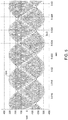
- Figure 5 illustrates a simulation of the time plot of the signals SHI and SLO.
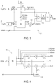
- the common-mode generator block 12 comprises a current calculation block 19 for calculating a reference current IREF, which represents the quadratic-mean current supplied by the three-phase source 3, as a function of the measured values of load currents ILM, of the values of reference voltage VREF, and of the measured values of input phase voltages VEM.
- the current calculation block 19 comprises a load-power calculation block 20, which supplies the power absorbed by the load (motor 5), designated by PL, as a function of measured values ILM and of the reference-voltage values VREF, and a mean-square calculation block 21 for calculating the mean-square value VE2 of the three-phase input voltage starting from the measured values VEM.
- the common-mode generator block 12 further comprises a first sample-ordering block 24, which compares with one another the values of each triad of values of the reference voltage VREF to identify at least the maximum value and the intermediate value of said triad of values and generate two corresponding signals of maximum voltage VREFmax and intermediate voltage VREFmid, and a second sample-ordering block 25, which compares with one another the values of each triad of the measured values ILM to supply at least the maximum value and the intermediate value of said triad of values and generate two corresponding signals of maximum current ILmax and intermediate current ILmid.
- the sample-ordering blocks 24 and 25 are similar to the sample-ordering block 16, with the difference that they act on triads of values of other quantities and supply only the corresponding maximum and intermediate values.
- condition for determining the current I1 is implemented via a switch 28 controlled by the comparator 27 and forming part of the calculation block 26.
- the common-mode voltage VCM is calculated by dividing the power P4 by the current 12 via a divider block 29 forming part of the calculation block 26.
- the condition that determines the current I1 requires knowledge of the result, i.e., of the common-mode voltage VCM.
- the calculation block 26 In order for the calculation block 26 to function in real time, it comprises a delay block 30 set between the output of the comparator 27 and the switch 28.
- the output of the comparator 27 switches between two values substantially equal to 1 and 0 and, instead of the switch 28, the calculation block 26 comprises a multiplier, which multiples the output of the comparator 27 by the signal ILmid.
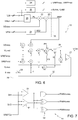
- the comparison and processing block 14 comprises, for each phase of the reference voltage VREFC, a pair of comparators 31 for comparing the phase of the reference voltage VREFC, designated by VREFCx in Figure 7 , where x is the generic output phase u, v, w of the matrix converter 1, with each of the modulated signals SHI and SLO, and a logic network 32 for determining three internal control signals PWMI corresponding to the phase x, designated by PWMIxmax, PWMIxmid, and PWMIxmin in Figure 7 , as a function of the logic outputs of the comparators 31.
- the control signal PWMIxmax refers to the voltage signal VEmax
- the control signal PWMIxmid refers to the voltage signal VEmid
- the control signal PWMIxmin refers to the voltage signal VEmin.
- Each of the nine control signals PWM is designated as a whole hereinafter by PWMyx, and each value of the triad of measured values of input voltage VEM is designated as a whole hereinafter by VEMy, where y and x are indices that represent, respectively, a generic input phase u, v, w and a generic output phase u, v, w of the matrix converter 1.
- the dynamic-mapping block 15 is configured for determining each control signal PWMyx from the internal control signals PWMIxmax, PWMIxmid, and PWMIxmin as a function of the comparison between the values VEMy of the triad of measured values VEM according to the logic described hereinafter.
- the signal PWMyx assumes the value of the signal PWMIxmax; otherwise, if the measured value VEMy is smaller than the values of the other input phases, i.e., basically if the value VEMy coincides with the value of the signal VEmin, then the signal PWMyx assumes the value of the signal PWMIxmin; otherwise, the signal PWMyx assumes the value of the signal PWMIxmid.
- Figure 8 illustrates a simulation of the time plot of a (star) phase output voltage, designated by VLx, of the matrix converter 1, said time plot being comprised between the time plots of the maximum value, designated by VLmax, and of the minimum value, designated by VLmin.
- VLx a (star) phase output voltage
- VLmin the minimum value
- the entire region comprised between the time plots of the maximum value VLmax and of the minimum value VLmin would be full of switchings.
- the percentage of the areas 31 with respect to the total area comprised between the maximum value VLmax and the minimum value VLmin within one period of the signal VLx is approximately 50%, to which there corresponds the same reduction in switching loss.
Landscapes
- Engineering & Computer Science (AREA)
- Power Engineering (AREA)
- Ac-Ac Conversion (AREA)
- Superconductors And Manufacturing Methods Therefor (AREA)
- Reduction Or Emphasis Of Bandwidth Of Signals (AREA)
Claims (11)
- Matrix-Direkt-AC/AC-Konverter, umfassend einen dreiphasigen Eingang (2), welcher mit einer dreiphasigen Eingangsspannung (VE) versorgt werden kann, einen dreiphasigen Ausgang (4), der an eine elektrische Last (5) angelegt werden kann, eine Vielzahl elektronischer Zwei-Wege-Schaltgeräte (6), welche so angeordnet sind, dass sie die Anschlüsse des dreiphasigen Eingangs (2) mit den Anschlüssen des dreiphasigen Ausgangs (4) matrixartig verbinden, und Steuermittel (7), um die Schaltgeräte (6) zu steuern; wobei die Steuermittel ausgelegt sind, um eine erste Referenzspannung (VREF) zu erhalten, welche eine gewünschte dreiphasige Spannung an dem dreiphasigen Ausgang (4) darstellt, und die Steuermittel (7) erste Verarbeitungsmittel (12) zum Generieren einer Gleichtaktspannung (VCM) und zweite Verarbeitungsmittel (13) zum Generieren einer zweiten Referenzspannung (VREFC) durch Kombinieren der ersten Referenzspannung (VREF) mit der Gleichtaktspannung (VCM) umfassen; wobei der Matrix-Direkt-AC/AC-Konverter dadurch gekennzeichnet ist, dass die Steuermittel (7) Spannungs- und Strommessmittel (8, 9) umfassen, zum Erhalt erster Messwerte (VEM) entsprechend dem dreiphasigen Eingang (VE) und zweiter Messwerte (ILM) entsprechend dem dreiphasigen Laststrom (IL), und dritte Verarbeitungsmittel (16, 24, 25) zum Verarbeiten der ersten Messwerte (VEM), um ein erstes Signal (VEmax), ein zweites Signal (VEmid), und ein drittes Signal (VEmin) zu erhalten, welche entsprechend Maximumwerte, Zwischenwerte und Minimumwerte der Phasen der dreiphasigen Eingangsspannung (VE) darstellen, und dass die ersten Verarbeitungsmittel (12) ausgelegt sind, um die Gleichtaktspannung (VCM) als Funktion der ersten Referenzspannung (VREF), der ersten und zweiten Messwerte (VEM, ILM) und der ersten, zweiten und dritten Signale (VEmax, VEmid, VEmin) zu generieren, und dass die Steuermittel (7) vierte Verarbeitungsmittel (10, 17, 18, 14) umfassen, um die ersten, zweiten und dritten Signale (VEmax, VEmid, VEmin) und die zweite Referenzspannung (VREFC) zu verarbeiten, um pulsweitenmodulierte interne Steuersignale (PWMI) zu erhalten, bezogen auf die ersten, zweiten und dritten Signale, und fünfte Verarbeitungsmittel (15) zum Generieren, anfangend mit den internen Steuersignalen (PWMI) und als eine Funktion eines Vergleichs zwischen den ersten Messwerten (VEM), pulsweitenmodulierter externer Steuersignale (PWM), die jeweils zum Steuern eines entsprechenden Zwei-Wege-Schalters (6) ausgelegt sind.
- Matrix-Direkt-AC/AC-Konverter, nach Anspruch 1, wobei die ersten Messwerte (VEM) erste Messwerttriaden umfassen, die den drei Phasen der dreiphasigen Eingangsspannung (VE) entsprechen; wobei die dritten Verarbeitungsmittel (16, 24, 25) erste Werteordnungsmittel (16) zum Identifizieren des Maximumwerts, des Minimumwerts und des übrigbleibenden Zwischenwerts jeder ersten Messwerttriade und zum Generieren des ersten Signals (VEmax), des dritten Signals (VEmin) und des zweiten Signals (VEmid), entsprechend mit dem Maximumwert, dem Minimumwert und dem Zwischenwert jeder ersten Messwerttriade umfassen.
- Matrix-Direkt-AC/AC-Konverter nach Anspruch 1 oder 2, wobei die ersten Verarbeitungsmittel (12) sechste Verarbeitungsmittel (19) zum Bestimmen eines Referenzstroms (IREF) umfassen, welcher den quadratischen Mittelstrom darstellt, der vom dreiphasigen Eingang (2) absorbiert wird, als eine Funktion der ersten Referenzspannung (VREF) und der ersten und zweiten Messwerte (VEM, ILM), und siebte Verarbeitungsmittel (26) zum Bestimmen der Gleichtaktspannung (VCM) als eine Funktion des Referenzstroms (IREF), der ersten Referenzspannung (VREF), der ersten und zweiten Signale (VEmax, VEmid) und von einem Teil der zweiten Messwerte (ILmax, ILmid).
- Matrix-Direkt-AC/AC-Konverter nach Anspruch 3, wobei die sechsten Verarbeitungsmittel (19) ausgebildet sind zum Berechnen einer Lastleistung (PL) als eine Funktion der ersten Referenzspannung (VREF) und der zweiten Messwerte (ILM), eines Mittelwertquadratwerts der Eingangsspannung (VE2) als eine Funktion der ersten Messwerte (VEM), eines Zwischenfaktors durch Multiplizieren der Lastleistung (PL) mit dem ersten Signal (VEmax), und des Referenzstroms (IREF) durch Dividieren des Zwischenfaktors durch den Mittelwertquadratwert (VE2).
- Matrix-Direkt-AC/AC-Konverter nach Anspruch 3 oder 4, wobei die zweiten Messwerte (ILM) zweite Messwerttriaden umfassen entsprechend den drei Phasen des Laststroms (IL), wobei die erste Referenzspannung durch eine Reihe von Spannungswerttriaden definiert wird; wobei die dritten Verarbeitungsmittel (16, 24, 25) zweite Werteordnungsmittel (24, 25) zum Identifizieren des Maximumwerts und des Zwischenwerts einer jeden zweiten Messwerttriade und des Maximumwerts und des Zwischenwerts einer jeden Spannungswerttriade und zum Generieren eines vierten Signals (ILmax) und eines fünften Signals (ILmid), entsprechend mit dem Maxiumwert und dem Zwischenwert einer jeden zweiten Messwerttriade, und eines sechsten Signals (VREFmax) und eines siebten Signals (VREFmid), entsprechend mit dem Maximumwert und mit dem Zwischenwert einer jeden Spannungswerttriade umfassen; wobei die siebten Verarbeitungsmittel (26) zum Bestimmen der Gleichtaktspannung (VCM) als eine Funktion des Referenzstroms (IREF) und des ersten Signals (VEmax), des zweiten Signals (VEmid), des vierten Signals (ILmax), des fünften Signals (ILmid), des sechsten Signals (VREFmax) und des siebten Signals (VREFmid) ausgebildet sind.
- Matrix-Direkt-AC/AC-Konverter nach einem der Ansprüche 1 bis 5, wobei die zweiten Verarbeitungsmittel (13) zum Erhalt der zweiten Referenzspannung (VREFC) durch Addieren der Gleichtaktspannung (VCM) zu jeder Phase der ersten Referenzspannung (VREF) ausgebildet sind.
- Matrix-Direkt-AC/AC-Konverter nach einem der Ansprüche 1 bis 6, wobei die vierten Verarbeitungsmittel (10, 17, 18, 14) signalgenerierende Mittel (10) zum Bereitstellen eines achten Signals (ST) mit Dreieckswellenform und einer festgelegten Frequenz umfassen, und achte Verarbeitungsmittel (17, 18) zum Bestimmen eines neunten Signals (SHI) und eines zehnten Signals (SLO) durch Modulieren des achten Signals (ST) mit zwei entsprechenden Kombinationen der ersten, zweiten und dritten Signale (VEmax, VEmid, VEmin).
- Matrix-Direkt-AC/AC-Konverter nach Anspruch 7, wobei die festgelegte Frequenz des achten Signals (ST) größer oder gleich 2 kHz ist.
- Matrix-Direkt-AC/AC-Konverter nach Anspruch 7 oder 8, wobei die neunten und zehnten Signale (SHI, SLO) auf Basis der folgenden Gleichungen bestimmt werden:


- Matrix-Direkt-AC/AC-Konverter nach einem der Ansprüche 7 bis 9, wobei die vierten Verarbeitungsmittel (10, 17, 18, 14) für jede Ausgangsphase (x) des dreiphasigen Ausgangs (4) ein Paar von Komparatoren (31) zum Vergleich der Ausgangsphase der zweiten Referenzspannung (VREFCx) mit jedem der neunten und zehnten Signale (SHI, SLO) umfassen und ein Logik-Netzwerk (32) zum Generieren, als eine Funktion der Logikausgänge der Komparatoren (31), dreier der internen Steuersignale (PWNIxmax, PWMIxmid, PWMIxmin), die der Ausgangsphase (x) entsprechen und sich entsprechend auf die ersten, zweiten und dritten Signale (VEmax, VEmid, VEmin) beziehen.
- Matrix-Direkt-AC/AC-Konverter nach Anspruch 10, wobei die ersten Messwerte (VEM) erste Messwerttriaden umfassen, die den drei Phasen der dreiphasigen Eingangsspannung (VE) entsprechen, und jedes der ersten externen Steuersignale (PWMyx) sich auf eine bestimmte Eingangsphase (y) des dreiphasigen Eingangs (2) und einer bestimmten Ausgangsphase (x) des Phasenausgangs (4) bezieht; wobei die fünften Verarbeitungsmittel (15) zum Bestimmen jedes der externen Steuersignale (PWMyx) durch Auswählen eines der internen Steuersignale (PWNIxmax, PWMIxmid, PWMIxmin), die der Ausgangsphase (x) als eine Funktion eines Vergleichs zwischen den Werten jeder ersten Messwerttriade entsprechen, ausgebildet sind.
Applications Claiming Priority (1)
| Application Number | Priority Date | Filing Date | Title |
|---|---|---|---|
| IT102016000084411A IT201600084411A1 (it) | 2016-08-10 | 2016-08-10 | Convertitore ac/ac diretto a matrice |
Publications (2)
| Publication Number | Publication Date |
|---|---|
| EP3285386A1 EP3285386A1 (de) | 2018-02-21 |
| EP3285386B1 true EP3285386B1 (de) | 2021-04-28 |
Family
ID=57906904
Family Applications (1)
| Application Number | Title | Priority Date | Filing Date |
|---|---|---|---|
| EP17185806.1A Active EP3285386B1 (de) | 2016-08-10 | 2017-08-10 | Matrixgleichstrom-wechselstromwandler |
Country Status (2)
| Country | Link |
|---|---|
| EP (1) | EP3285386B1 (de) |
| IT (1) | IT201600084411A1 (de) |
Families Citing this family (1)
| Publication number | Priority date | Publication date | Assignee | Title |
|---|---|---|---|---|
| CN116819316A (zh) * | 2023-06-30 | 2023-09-29 | 哈尔滨理工大学 | 基于模型预测控制的三相永磁同步电机驱动系统故障诊断方法 |
Family Cites Families (2)
| Publication number | Priority date | Publication date | Assignee | Title |
|---|---|---|---|---|
| IT1167285B (it) | 1983-12-05 | 1987-05-13 | Venturini Marco G B | Metodo e apparecchiatura per la conversione di un sistema di tensioni polifase |
| US4833588A (en) * | 1988-08-31 | 1989-05-23 | Westinghouse Electric Corp. | Direct AC/AC converter system |
-
2016
- 2016-08-10 IT IT102016000084411A patent/IT201600084411A1/it unknown
-
2017
- 2017-08-10 EP EP17185806.1A patent/EP3285386B1/de active Active
Non-Patent Citations (1)
| Title |
|---|
| None * |
Also Published As
| Publication number | Publication date |
|---|---|
| EP3285386A1 (de) | 2018-02-21 |
| IT201600084411A1 (it) | 2018-02-10 |
Similar Documents
| Publication | Publication Date | Title |
|---|---|---|
| Jacobina et al. | AC motor drive systems with a reduced-switch-count converter | |
| Shen et al. | Fixed-frequency space-vector-modulation control for three-phase four-leg active power filters | |
| Hava et al. | Performance analysis of reduced common-mode voltage PWM methods and comparison with standard PWM methods for three-phase voltage-source inverters | |
| Charumit et al. | Discontinuous SVPWM techniques of three-leg VSI-fed balanced two-phase loads for reduced switching losses and current ripple | |
| Hamidi et al. | An asymmetrical multilevel inverter with optimum number of components based on new basic structure for photovoltaic renewable energy system | |
| KR20160013176A (ko) | 병렬로 접속된 다단 컨버터들을 가지는 컨버터 어셈블리 및 상기 다단 컨버터들을 제어하기 위한 방법 | |
| Kim et al. | Pulsewidth modulation method of matrix converter for reducing output current ripple | |
| CN108476011A (zh) | 电动机的控制装置和驱动系统 | |
| EP2887517A1 (de) | Verfahren zum Ansteuern eines mehrstufigen Mehrphasenwechselrichters | |
| Dekka et al. | Voltage balancing of a modular neutral-point-clamped converter with a carrier-based modulation scheme | |
| Bohra et al. | Modulation techniques in single phase PWM rectifier | |
| Szczesniak et al. | Comparative study of drive systems using vector-controlled PMSM fed by a matrix converter and a conventional frequency converter | |
| Zhang | Investigation of switching schemes for three-phase four-leg voltage source inverters | |
| Zaamouche et al. | A discontinuous PWM techniques evaluation by analysis of voltage and current waveforms | |
| WO2018179234A1 (ja) | H型ブリッジ変換器およびパワーコンディショナ | |
| EP3285386A1 (de) | Matrixgleichstrom-wechselstromwandler | |
| Jacob et al. | Hardware realization and analysis of a seven level reduced switch inverter with space vector modulation technique | |
| Iqbal et al. | Pulse‐Width Modulation of Power Electronic DC–AC Converter | |
| KR101648002B1 (ko) | 3상 3레벨 정류기를 위한 스위칭 신호 발생기 및 스위칭 신호 발생 방법 | |
| Alzuabidi | Study and implementation sinusoidal PWM inverter fed 3-phase induction motor | |
| Nguyen et al. | A carrier-based pulse width modulation method for indirect matrix converters | |
| Babu et al. | High performance direct torque controlled induction motor drive for adjustable speed drive applications | |
| Colak et al. | Practical implementation of a digital signal processor controlled multilevel inverter with low total harmonic distortion for motor drive applications | |
| Sharma et al. | Performance Analysis of Five Level Cascaded H Bridge SPWM Inverter Fed Five Phase Induction Motor Drives | |
| Potamianos et al. | A fault tolerant modulation strategy for matrix converters |
Legal Events
| Date | Code | Title | Description |
|---|---|---|---|
| PUAI | Public reference made under article 153(3) epc to a published international application that has entered the european phase |
Free format text: ORIGINAL CODE: 0009012 |
|
| STAA | Information on the status of an ep patent application or granted ep patent |
Free format text: STATUS: THE APPLICATION HAS BEEN PUBLISHED |
|
| AK | Designated contracting states |
Kind code of ref document: A1 Designated state(s): AL AT BE BG CH CY CZ DE DK EE ES FI FR GB GR HR HU IE IS IT LI LT LU LV MC MK MT NL NO PL PT RO RS SE SI SK SM TR |
|
| AX | Request for extension of the european patent |
Extension state: BA ME |
|
| STAA | Information on the status of an ep patent application or granted ep patent |
Free format text: STATUS: REQUEST FOR EXAMINATION WAS MADE |
|
| 17P | Request for examination filed |
Effective date: 20180820 |
|
| RBV | Designated contracting states (corrected) |
Designated state(s): AL AT BE BG CH CY CZ DE DK EE ES FI FR GB GR HR HU IE IS IT LI LT LU LV MC MK MT NL NO PL PT RO RS SE SI SK SM TR |
|
| RIC1 | Information provided on ipc code assigned before grant |
Ipc: H02M 1/12 20060101ALN20201008BHEP Ipc: H02M 5/297 20060101AFI20201008BHEP |
|
| GRAP | Despatch of communication of intention to grant a patent |
Free format text: ORIGINAL CODE: EPIDOSNIGR1 |
|
| STAA | Information on the status of an ep patent application or granted ep patent |
Free format text: STATUS: GRANT OF PATENT IS INTENDED |
|
| INTG | Intention to grant announced |
Effective date: 20201118 |
|
| RAP1 | Party data changed (applicant data changed or rights of an application transferred) |
Owner name: PHASE MOTION CONTROL S.P.A. |
|
| RAP1 | Party data changed (applicant data changed or rights of an application transferred) |
Owner name: PHASE MOTION CONTROL S.P.A. |
|
| GRAS | Grant fee paid |
Free format text: ORIGINAL CODE: EPIDOSNIGR3 |
|
| GRAA | (expected) grant |
Free format text: ORIGINAL CODE: 0009210 |
|
| STAA | Information on the status of an ep patent application or granted ep patent |
Free format text: STATUS: THE PATENT HAS BEEN GRANTED |
|
| AK | Designated contracting states |
Kind code of ref document: B1 Designated state(s): AL AT BE BG CH CY CZ DE DK EE ES FI FR GB GR HR HU IE IS IT LI LT LU LV MC MK MT NL NO PL PT RO RS SE SI SK SM TR |
|
| REG | Reference to a national code |
Ref country code: GB Ref legal event code: FG4D |
|
| REG | Reference to a national code |
Ref country code: CH Ref legal event code: EP |
|
| REG | Reference to a national code |
Ref country code: AT Ref legal event code: REF Ref document number: 1388268 Country of ref document: AT Kind code of ref document: T Effective date: 20210515 |
|
| REG | Reference to a national code |
Ref country code: DE Ref legal event code: R096 Ref document number: 602017037469 Country of ref document: DE |
|
| REG | Reference to a national code |
Ref country code: IE Ref legal event code: FG4D |
|
| REG | Reference to a national code |
Ref country code: LT Ref legal event code: MG9D |
|
| REG | Reference to a national code |
Ref country code: AT Ref legal event code: MK05 Ref document number: 1388268 Country of ref document: AT Kind code of ref document: T Effective date: 20210428 |
|
| PG25 | Lapsed in a contracting state [announced via postgrant information from national office to epo] |
Ref country code: HR Free format text: LAPSE BECAUSE OF FAILURE TO SUBMIT A TRANSLATION OF THE DESCRIPTION OR TO PAY THE FEE WITHIN THE PRESCRIBED TIME-LIMIT Effective date: 20210428 Ref country code: AT Free format text: LAPSE BECAUSE OF FAILURE TO SUBMIT A TRANSLATION OF THE DESCRIPTION OR TO PAY THE FEE WITHIN THE PRESCRIBED TIME-LIMIT Effective date: 20210428 Ref country code: BG Free format text: LAPSE BECAUSE OF FAILURE TO SUBMIT A TRANSLATION OF THE DESCRIPTION OR TO PAY THE FEE WITHIN THE PRESCRIBED TIME-LIMIT Effective date: 20210728 Ref country code: NL Free format text: LAPSE BECAUSE OF FAILURE TO SUBMIT A TRANSLATION OF THE DESCRIPTION OR TO PAY THE FEE WITHIN THE PRESCRIBED TIME-LIMIT Effective date: 20210428 Ref country code: FI Free format text: LAPSE BECAUSE OF FAILURE TO SUBMIT A TRANSLATION OF THE DESCRIPTION OR TO PAY THE FEE WITHIN THE PRESCRIBED TIME-LIMIT Effective date: 20210428 Ref country code: LT Free format text: LAPSE BECAUSE OF FAILURE TO SUBMIT A TRANSLATION OF THE DESCRIPTION OR TO PAY THE FEE WITHIN THE PRESCRIBED TIME-LIMIT Effective date: 20210428 |
|
| PG25 | Lapsed in a contracting state [announced via postgrant information from national office to epo] |
Ref country code: PL Free format text: LAPSE BECAUSE OF FAILURE TO SUBMIT A TRANSLATION OF THE DESCRIPTION OR TO PAY THE FEE WITHIN THE PRESCRIBED TIME-LIMIT Effective date: 20210428 Ref country code: PT Free format text: LAPSE BECAUSE OF FAILURE TO SUBMIT A TRANSLATION OF THE DESCRIPTION OR TO PAY THE FEE WITHIN THE PRESCRIBED TIME-LIMIT Effective date: 20210830 Ref country code: NO Free format text: LAPSE BECAUSE OF FAILURE TO SUBMIT A TRANSLATION OF THE DESCRIPTION OR TO PAY THE FEE WITHIN THE PRESCRIBED TIME-LIMIT Effective date: 20210728 Ref country code: SE Free format text: LAPSE BECAUSE OF FAILURE TO SUBMIT A TRANSLATION OF THE DESCRIPTION OR TO PAY THE FEE WITHIN THE PRESCRIBED TIME-LIMIT Effective date: 20210428 Ref country code: RS Free format text: LAPSE BECAUSE OF FAILURE TO SUBMIT A TRANSLATION OF THE DESCRIPTION OR TO PAY THE FEE WITHIN THE PRESCRIBED TIME-LIMIT Effective date: 20210428 Ref country code: IS Free format text: LAPSE BECAUSE OF FAILURE TO SUBMIT A TRANSLATION OF THE DESCRIPTION OR TO PAY THE FEE WITHIN THE PRESCRIBED TIME-LIMIT Effective date: 20210828 Ref country code: LV Free format text: LAPSE BECAUSE OF FAILURE TO SUBMIT A TRANSLATION OF THE DESCRIPTION OR TO PAY THE FEE WITHIN THE PRESCRIBED TIME-LIMIT Effective date: 20210428 Ref country code: GR Free format text: LAPSE BECAUSE OF FAILURE TO SUBMIT A TRANSLATION OF THE DESCRIPTION OR TO PAY THE FEE WITHIN THE PRESCRIBED TIME-LIMIT Effective date: 20210729 |
|
| REG | Reference to a national code |
Ref country code: NL Ref legal event code: MP Effective date: 20210428 |
|
| PG25 | Lapsed in a contracting state [announced via postgrant information from national office to epo] |
Ref country code: SK Free format text: LAPSE BECAUSE OF FAILURE TO SUBMIT A TRANSLATION OF THE DESCRIPTION OR TO PAY THE FEE WITHIN THE PRESCRIBED TIME-LIMIT Effective date: 20210428 Ref country code: SM Free format text: LAPSE BECAUSE OF FAILURE TO SUBMIT A TRANSLATION OF THE DESCRIPTION OR TO PAY THE FEE WITHIN THE PRESCRIBED TIME-LIMIT Effective date: 20210428 Ref country code: CZ Free format text: LAPSE BECAUSE OF FAILURE TO SUBMIT A TRANSLATION OF THE DESCRIPTION OR TO PAY THE FEE WITHIN THE PRESCRIBED TIME-LIMIT Effective date: 20210428 Ref country code: DK Free format text: LAPSE BECAUSE OF FAILURE TO SUBMIT A TRANSLATION OF THE DESCRIPTION OR TO PAY THE FEE WITHIN THE PRESCRIBED TIME-LIMIT Effective date: 20210428 Ref country code: EE Free format text: LAPSE BECAUSE OF FAILURE TO SUBMIT A TRANSLATION OF THE DESCRIPTION OR TO PAY THE FEE WITHIN THE PRESCRIBED TIME-LIMIT Effective date: 20210428 Ref country code: ES Free format text: LAPSE BECAUSE OF FAILURE TO SUBMIT A TRANSLATION OF THE DESCRIPTION OR TO PAY THE FEE WITHIN THE PRESCRIBED TIME-LIMIT Effective date: 20210428 Ref country code: RO Free format text: LAPSE BECAUSE OF FAILURE TO SUBMIT A TRANSLATION OF THE DESCRIPTION OR TO PAY THE FEE WITHIN THE PRESCRIBED TIME-LIMIT Effective date: 20210428 |
|
| REG | Reference to a national code |
Ref country code: DE Ref legal event code: R097 Ref document number: 602017037469 Country of ref document: DE |
|
| PLBE | No opposition filed within time limit |
Free format text: ORIGINAL CODE: 0009261 |
|
| STAA | Information on the status of an ep patent application or granted ep patent |
Free format text: STATUS: NO OPPOSITION FILED WITHIN TIME LIMIT |
|
| REG | Reference to a national code |
Ref country code: CH Ref legal event code: PL |
|
| PG25 | Lapsed in a contracting state [announced via postgrant information from national office to epo] |
Ref country code: MC Free format text: LAPSE BECAUSE OF FAILURE TO SUBMIT A TRANSLATION OF THE DESCRIPTION OR TO PAY THE FEE WITHIN THE PRESCRIBED TIME-LIMIT Effective date: 20210428 |
|
| 26N | No opposition filed |
Effective date: 20220131 |
|
| REG | Reference to a national code |
Ref country code: BE Ref legal event code: MM Effective date: 20210831 |
|
| PG25 | Lapsed in a contracting state [announced via postgrant information from national office to epo] |
Ref country code: LI Free format text: LAPSE BECAUSE OF NON-PAYMENT OF DUE FEES Effective date: 20210831 Ref country code: CH Free format text: LAPSE BECAUSE OF NON-PAYMENT OF DUE FEES Effective date: 20210831 |
|
| PG25 | Lapsed in a contracting state [announced via postgrant information from national office to epo] |
Ref country code: IS Free format text: LAPSE BECAUSE OF FAILURE TO SUBMIT A TRANSLATION OF THE DESCRIPTION OR TO PAY THE FEE WITHIN THE PRESCRIBED TIME-LIMIT Effective date: 20210828 Ref country code: AL Free format text: LAPSE BECAUSE OF FAILURE TO SUBMIT A TRANSLATION OF THE DESCRIPTION OR TO PAY THE FEE WITHIN THE PRESCRIBED TIME-LIMIT Effective date: 20210428 Ref country code: LU Free format text: LAPSE BECAUSE OF NON-PAYMENT OF DUE FEES Effective date: 20210810 |
|
| PG25 | Lapsed in a contracting state [announced via postgrant information from national office to epo] |
Ref country code: IT Free format text: LAPSE BECAUSE OF FAILURE TO SUBMIT A TRANSLATION OF THE DESCRIPTION OR TO PAY THE FEE WITHIN THE PRESCRIBED TIME-LIMIT Effective date: 20210428 Ref country code: IE Free format text: LAPSE BECAUSE OF NON-PAYMENT OF DUE FEES Effective date: 20210810 Ref country code: BE Free format text: LAPSE BECAUSE OF NON-PAYMENT OF DUE FEES Effective date: 20210831 |
|
| PG25 | Lapsed in a contracting state [announced via postgrant information from national office to epo] |
Ref country code: HU Free format text: LAPSE BECAUSE OF FAILURE TO SUBMIT A TRANSLATION OF THE DESCRIPTION OR TO PAY THE FEE WITHIN THE PRESCRIBED TIME-LIMIT; INVALID AB INITIO Effective date: 20170810 |
|
| PG25 | Lapsed in a contracting state [announced via postgrant information from national office to epo] |
Ref country code: CY Free format text: LAPSE BECAUSE OF FAILURE TO SUBMIT A TRANSLATION OF THE DESCRIPTION OR TO PAY THE FEE WITHIN THE PRESCRIBED TIME-LIMIT Effective date: 20210428 |
|
| PG25 | Lapsed in a contracting state [announced via postgrant information from national office to epo] |
Ref country code: MK Free format text: LAPSE BECAUSE OF FAILURE TO SUBMIT A TRANSLATION OF THE DESCRIPTION OR TO PAY THE FEE WITHIN THE PRESCRIBED TIME-LIMIT Effective date: 20210428 |
|
| PG25 | Lapsed in a contracting state [announced via postgrant information from national office to epo] |
Ref country code: MT Free format text: LAPSE BECAUSE OF FAILURE TO SUBMIT A TRANSLATION OF THE DESCRIPTION OR TO PAY THE FEE WITHIN THE PRESCRIBED TIME-LIMIT Effective date: 20210428 |
|
| PGFP | Annual fee paid to national office [announced via postgrant information from national office to epo] |
Ref country code: GB Payment date: 20240827 Year of fee payment: 8 |
|
| PGFP | Annual fee paid to national office [announced via postgrant information from national office to epo] |
Ref country code: FR Payment date: 20240826 Year of fee payment: 8 |
|
| PGFP | Annual fee paid to national office [announced via postgrant information from national office to epo] |
Ref country code: DE Payment date: 20250827 Year of fee payment: 9 |
|
| PG25 | Lapsed in a contracting state [announced via postgrant information from national office to epo] |
Ref country code: TR Free format text: LAPSE BECAUSE OF FAILURE TO SUBMIT A TRANSLATION OF THE DESCRIPTION OR TO PAY THE FEE WITHIN THE PRESCRIBED TIME-LIMIT Effective date: 20210428 |
|
| GBPC | Gb: european patent ceased through non-payment of renewal fee |
Effective date: 20250810 |