EP3285151A1 - Electromagnetic induction-type position detection sensor - Google Patents
Electromagnetic induction-type position detection sensor Download PDFInfo
- Publication number
- EP3285151A1 EP3285151A1 EP16780056.4A EP16780056A EP3285151A1 EP 3285151 A1 EP3285151 A1 EP 3285151A1 EP 16780056 A EP16780056 A EP 16780056A EP 3285151 A1 EP3285151 A1 EP 3285151A1
- Authority
- EP
- European Patent Office
- Prior art keywords
- wiring path
- section
- face
- position detection
- detection sensor
- Prior art date
- Legal status (The legal status is an assumption and is not a legal conclusion. Google has not performed a legal analysis and makes no representation as to the accuracy of the status listed.)
- Granted
Links
Images




Classifications
-
- G—PHYSICS
- G01—MEASURING; TESTING
- G01B—MEASURING LENGTH, THICKNESS OR SIMILAR LINEAR DIMENSIONS; MEASURING ANGLES; MEASURING AREAS; MEASURING IRREGULARITIES OF SURFACES OR CONTOURS
- G01B7/00—Measuring arrangements characterised by the use of electric or magnetic techniques
- G01B7/003—Measuring arrangements characterised by the use of electric or magnetic techniques for measuring position, not involving coordinate determination
-
- G—PHYSICS
- G06—COMPUTING OR CALCULATING; COUNTING
- G06F—ELECTRIC DIGITAL DATA PROCESSING
- G06F3/00—Input arrangements for transferring data to be processed into a form capable of being handled by the computer; Output arrangements for transferring data from processing unit to output unit, e.g. interface arrangements
- G06F3/01—Input arrangements or combined input and output arrangements for interaction between user and computer
- G06F3/03—Arrangements for converting the position or the displacement of a member into a coded form
- G06F3/041—Digitisers, e.g. for touch screens or touch pads, characterised by the transducing means
- G06F3/0416—Control or interface arrangements specially adapted for digitisers
- G06F3/04164—Connections between sensors and controllers, e.g. routing lines between electrodes and connection pads
-
- G—PHYSICS
- G06—COMPUTING OR CALCULATING; COUNTING
- G06F—ELECTRIC DIGITAL DATA PROCESSING
- G06F3/00—Input arrangements for transferring data to be processed into a form capable of being handled by the computer; Output arrangements for transferring data from processing unit to output unit, e.g. interface arrangements
- G06F3/01—Input arrangements or combined input and output arrangements for interaction between user and computer
- G06F3/03—Arrangements for converting the position or the displacement of a member into a coded form
- G06F3/041—Digitisers, e.g. for touch screens or touch pads, characterised by the transducing means
- G06F3/046—Digitisers, e.g. for touch screens or touch pads, characterised by the transducing means by electromagnetic means
-
- H—ELECTRICITY
- H05—ELECTRIC TECHNIQUES NOT OTHERWISE PROVIDED FOR
- H05K—PRINTED CIRCUITS; CASINGS OR CONSTRUCTIONAL DETAILS OF ELECTRIC APPARATUS; MANUFACTURE OF ASSEMBLAGES OF ELECTRICAL COMPONENTS
- H05K3/00—Apparatus or processes for manufacturing printed circuits
- H05K3/10—Apparatus or processes for manufacturing printed circuits in which conductive material is applied to the insulating support in such a manner as to form the desired conductive pattern
-
- H—ELECTRICITY
- H05—ELECTRIC TECHNIQUES NOT OTHERWISE PROVIDED FOR
- H05K—PRINTED CIRCUITS; CASINGS OR CONSTRUCTIONAL DETAILS OF ELECTRIC APPARATUS; MANUFACTURE OF ASSEMBLAGES OF ELECTRICAL COMPONENTS
- H05K3/00—Apparatus or processes for manufacturing printed circuits
- H05K3/30—Assembling printed circuits with electric components, e.g. with resistors
- H05K3/32—Assembling printed circuits with electric components, e.g. with resistors electrically connecting electric components or wires to printed circuits
- H05K3/34—Assembling printed circuits with electric components, e.g. with resistors electrically connecting electric components or wires to printed circuits by soldering
- H05K3/341—Surface mounted components
-
- G—PHYSICS
- G06—COMPUTING OR CALCULATING; COUNTING
- G06F—ELECTRIC DIGITAL DATA PROCESSING
- G06F2203/00—Indexing scheme relating to G06F3/00 - G06F3/048
- G06F2203/041—Indexing scheme relating to G06F3/041 - G06F3/045
- G06F2203/04103—Manufacturing, i.e. details related to manufacturing processes specially suited for touch sensitive devices
-
- H—ELECTRICITY
- H05—ELECTRIC TECHNIQUES NOT OTHERWISE PROVIDED FOR
- H05K—PRINTED CIRCUITS; CASINGS OR CONSTRUCTIONAL DETAILS OF ELECTRIC APPARATUS; MANUFACTURE OF ASSEMBLAGES OF ELECTRICAL COMPONENTS
- H05K1/00—Printed circuits
- H05K1/02—Details
- H05K1/09—Use of materials for the conductive, e.g. metallic pattern
- H05K1/092—Dispersed materials, e.g. conductive pastes or inks
- H05K1/095—Dispersed materials, e.g. conductive pastes or inks for polymer thick films, i.e. having a permanent organic polymeric binder
-
- H—ELECTRICITY
- H05—ELECTRIC TECHNIQUES NOT OTHERWISE PROVIDED FOR
- H05K—PRINTED CIRCUITS; CASINGS OR CONSTRUCTIONAL DETAILS OF ELECTRIC APPARATUS; MANUFACTURE OF ASSEMBLAGES OF ELECTRICAL COMPONENTS
- H05K1/00—Printed circuits
- H05K1/16—Printed circuits incorporating printed electric components, e.g. printed resistors, capacitors or inductors
-
- H—ELECTRICITY
- H05—ELECTRIC TECHNIQUES NOT OTHERWISE PROVIDED FOR
- H05K—PRINTED CIRCUITS; CASINGS OR CONSTRUCTIONAL DETAILS OF ELECTRIC APPARATUS; MANUFACTURE OF ASSEMBLAGES OF ELECTRICAL COMPONENTS
- H05K2201/00—Indexing scheme relating to printed circuits covered by H05K1/00
- H05K2201/10—Details of components or other objects attached to or integrated in a printed circuit board
- H05K2201/10007—Types of components
- H05K2201/10151—Sensor
-
- H—ELECTRICITY
- H05—ELECTRIC TECHNIQUES NOT OTHERWISE PROVIDED FOR
- H05K—PRINTED CIRCUITS; CASINGS OR CONSTRUCTIONAL DETAILS OF ELECTRIC APPARATUS; MANUFACTURE OF ASSEMBLAGES OF ELECTRICAL COMPONENTS
- H05K3/00—Apparatus or processes for manufacturing printed circuits
- H05K3/10—Apparatus or processes for manufacturing printed circuits in which conductive material is applied to the insulating support in such a manner as to form the desired conductive pattern
- H05K3/12—Apparatus or processes for manufacturing printed circuits in which conductive material is applied to the insulating support in such a manner as to form the desired conductive pattern using thick film techniques, e.g. printing techniques to apply the conductive material or similar techniques for applying conductive paste or ink patterns
- H05K3/1216—Apparatus or processes for manufacturing printed circuits in which conductive material is applied to the insulating support in such a manner as to form the desired conductive pattern using thick film techniques, e.g. printing techniques to apply the conductive material or similar techniques for applying conductive paste or ink patterns by screen printing or stencil printing
Definitions
- the present invention relates to an electromagnetic induction position detection sensor.
- An electromagnetic induction position detection sensor is formed by a number of loop coils disposed in X-axis and Y-axis directions of coordinate axes on a board.
- a position detection device having a position detection sensor permits detection of coordinates of a position pointed to by a position pointer in the X-axis and Y-axis directions based on electromagnetic induction action between the position pointer and the position detection sensor.
- Metal paste used not only for position detection sensors but also for ordinary circuit boards includes metallic powder and a resin binder (bonding agent). Then, metal paste applied to the circuit board is subjected to a thermal treatment so that conductivity is enhanced by fusing the metal powder to each other.
- Heat-resistant polyimide-based resin sheet is used as a board material on which to screen-print a metal paste.
- a metal particularly used as a metal powder of metal paste, is silver.
- a position detection sensor having a board coated with silver paste through screen printing offers high conductivity and can be fabricated by heating at approximately 200°C to 250°C, relatively low temperatures for a thermal treatment, for approximately 20 to 30 minutes, and, therefore, has become popular.
- fabricating a position detection sensor using silver paste had the following problems.
- silver paste was expensive, resulting in higher cost than conventional copper etching.
- it is necessary to reduce a loop coil width and a spacing between the loop coils to the extent possible.
- silver paste is used, the coil spacing cannot be reduced due to ion migration phenomenon. This has led to a problem characterized by difficulties in fabricating compact position detection sensors using silver paste.
- Patent Document 2 Japanese Patent Laid-Open No. Hei 9-55568 .
- Patent Document 2 there was a problem with applying the method of Patent Document 2 in an 'as-is' fashion to a position detection sensor. That is, wiring is printed on both faces to eliminate warping of the board. However, if there is an imbalance in wiring between one face the other face, wrinkles and undulations occur.
- FIG. 10(A) no problem arose if wiring paths 2 made of copper paste were successfully formed, one on one face 1a and another on another face 1b, at positions opposed to each other on a sheet-shaped board 1.
- FIG. 10(B) in the event of an unevenness between positions of the wiring paths 2 due to misalignment from the opposing positions, the binder shrank, causing an undulation problem as depicted in FIG. 10(C) .
- a position detection sensor has areas where wiring is partially concentrated and areas where wiring is distributed unevenly in one direction such as a connector section between the position detection sensor and a position detection circuit. In such areas, wrinkle and undulation problems occurred despite wiring printed on both faces using the method described in Patent Document 2.
- the invention of claim 1 provides an electromagnetic induction position detection sensor that has a wiring path pattern made of copper paste that includes copper powder and a binder formed on a sheet-shaped board made of resin and that has a plurality of position detection loop coils formed by thermally treating the wiring path pattern.
- the wiring path pattern is configured to include the position detection loop coils and a connector section for connection between the position detection loop coils and external circuitry.
- the wiring path pattern made of the copper paste is formed to extend in a first direction, and the wiring path pattern formed to extend in the first direction is formed to extend in a second direction orthogonal to the first direction at a given pitch.
- the wiring path pattern made of the copper paste is formed to extend in the second direction, and the wiring path pattern formed to extend in the second direction is formed to extend in the first direction at a given pitch. Further, a wiring path pattern is disposed on the one face and the other face in the connector section.
- the plurality of wiring patterns formed to extend in the first direction on the one face of the sheet-shaped board are formed in the second direction at the given pitch, and the plurality of wiring patterns formed to extend in the second direction on the other face of the sheet-shaped board are formed in the first direction at the given pitch. Therefore, the plurality of wiring path patterns made of the copper paste are formed in the directions orthogonal to each other on the one face and the other face of the sheet-shaped board.
- the plurality of wiring patterns formed on both faces of the sheet-shaped board are each formed at the given pitch.
- lattices of a given size are formed evenly approximately across the entire sheet-shaped board thanks to the plurality of wiring path patterns on both faces of the sheet-shaped board. Therefore, even in the event of shrinkage of the copper paste binder due to thermal treatment, that shrinkage takes place evenly approximately across the entire sheet-shaped board, ensuring freedom from partial warping or undulation. This makes it possible to provide a position detection sensor that offers high accuracy even when copper paste is used.
- the invention of claim 2 is characterized in that, in the invention of claim 1, the connector section is provided, at a given end portion of the sheet-shaped board, in which extended portions of lead wiring paths from a loop section of the position detection loop coils are formed. Wiring path patterns in the directions orthogonal to each other are also substantially formed on the one face and the other face of the sheet-shaped board in the connector section.
- patterns made of the copper paste are also substantially formed in the directions orthogonal to each other on one face and another face of the connector section. Therefore, in the connector section, even in the event of shrinkage of the copper paste binder in the wiring path patterns orthogonal to each other, the connector section as a whole shrinks evenly, preventing warping or undulation of the connector section.
- the electromagnetic induction position detection sensor has an effect in that if loop coils are formed on a sheet-shaped board made of a polyimide-based resin using copper paste, and even in the event of shrinkage of a binder included in the copper paste by a thermal treatment, that shrinkage takes place evenly approximately across the entire sheet-shaped board, and as a result, the sheet-shaped board is kept free from partial warping or undulation.
- the position detection sensor also has an effect in that accuracy can be maintained.
- a pen-type position pointer 300 used together with an electromagnetic induction coordinate input device 200 in this example incorporates a parallel resonance circuit that includes a coil 301 and a capacitor 302 connected in parallel to the coil 301 as illustrated in FIG. 2 .
- a loop coil group 21 running in the X-axis direction and a loop coil group 22 running in the Y-axis direction are disposed on each of top and rear faces of a sheet-shaped board 23 made of polyimide-based resin in such a manner as to spatially overlap each other as illustrated in FIG. 2 .
- the direction across the board of the position detection sensor 20 is assumed to be the X-axis direction
- the direction down the board of the position detection sensor 20 is assumed to be the Y-axis direction.
- the loop coil group 21 running in the X-axis direction includes n (where n is an integer equal to 2 or more) rectangular loop coils 21X 1 to 21X n that are arranged at a given pitch in the X-axis direction
- the loop coil group 22 running in the Y-axis direction includes m (where m is an integer equal to 2 or more) loop coils 22Y 1 to 22Y m that are arranged at a given pitch in the Y-axis direction.
- a position detection area 25 includes a loop section of the loop coil group 21 running in the X-axis direction and a loop section of the loop coil group 22 running in the Y-axis direction.
- Each one of the wiring paths (return wiring path which will be described later) is connected to each other as illustrated in FIG. 2 and connected to a terminal supplied with a reference potential, a ground terminal in the example depicted in FIG. 2 .
- the position detection sensor 20 is connected to a position detection circuit 210 via a connector section that is omitted in the figure.
- the position detection circuit 210 includes a selection circuit 211, an oscillator 212, a current driver 213, a transmission/reception switching circuit 214, a receiving amplifier 215, a detection circuit 216, a low-pass filter 217, a sample-hold circuit 218, an analog to digital (A/D) conversion circuit 219, and a processing control section 220.
- the X-axis direction loop coil group 21 and the Y-axis direction loop coil group 22 are connected by the selection circuit 211.
- the selection circuit 211 successively selects one of the loop coils of the two loop coil groups 21 and 22 in accordance with a control instruction from the processing control section 220.
- the oscillator 212 generates an alternate current (AC) signal at a frequency f0.
- This AC signal is supplied to the current driver 213 for conversion into a current and then sent to the transmission/reception switching circuit 214.
- the transmission/reception switching circuit 214 switches, every given time period, between connection destinations (transmitting side terminal T and receiving side terminal R) to which the loop coil selected by the selection circuit 211 is connected under control of the processing control section 220.
- the current driver 213 is connected to the transmitting side terminal T, and the receiving amplifier 215 is connected to the receiving side terminal R.
- the AC signal from the current driver 213 is supplied to the loop coil selected by the selection circuit 211 via the transmitting side terminal T of the transmission/reception switching circuit 214.
- the induced voltage generated in the loop coil selected by the selection circuit 211 is supplied to the receiving amplifier 215 via the selection circuit 211 and the receiving side terminal R of the transmission/reception switching circuit 214 for amplification and sent to the detection circuit 216.
- the signal detected by the detection circuit 216 is supplied to the A/D conversion circuit 219 via the low-pass filter 217 and the sample-hold circuit 218.
- the A/D conversion circuit 219 converts the analog signal into a digital signal and supplies the signal to the processing control section 220.
- the processing control section 220 performs control for position detection. That is, the processing control section 220 controls loop coil selection by the selection circuit 211, signal switching by the transmission/reception switching circuit 214, timings of the sample-hold circuit 218, and so on.
- the processing control section 220 controls energization of the loop coil selected by the selection circuit 211 of the X-axis direction loop coil group 21 or the Y-axis direction loop coil group 22 to send electromagnetic waves by switching the transmission/reception switching circuit 214 for connection to the transmitting side terminal T.
- the resonance circuit of the position pointer 300 receives electromagnetic waves sent from this loop coil and stores energy.
- the processing control section 220 switches the transmission/reception switching circuit 214 for connection to the receiving side terminal R. Then, an induced voltage is generated in each of the loop coils of the X-axis direction loop coil group 21 and the Y-axis direction loop coil group 22 by electromagnetic waves sent from the position pointer 300.
- the processing control section 220 calculates coordinate values of the position pointed to in the X-axis and Y-axis directions in a position detection area 25 of the position detection sensor 20 based on the voltage level of the induced voltage generated in each of the loop coils. Then, the processing control section 220 supplies calculated coordinate value information, for example, to an external personal computer.
- FIG. 1 depicts diagrams for describing a position detection sensor 20A of the first embodiment applied to the position detection sensor 20 illustrated in FIG. 2 .
- This drawing is intended to describe how each of loop coils 21X i (where i is any one of 1, 2 and so on up to n) of the X-axis direction loop coil group 21 and each of loop coils 22Yj (where j is any one of 1, 2 and so on up to m) of the Y-axis direction loop coil group 22 are formed with respect to the sheet-shaped board 23.
- FIG. 1(A) is a view as seen from the side of one face 23a of the board 23, and FIG. 1(B) is a view as seen from a direction vertical to the face 23a of the board 23.
- illustration of a conductor pattern making up the loop coils 21X i and 22Y j is omitted.
- the sheet-shaped board 23 in this example is a thin film-shaped flexible board made of polyimide-based resin. Then, straight line portions X i La and X i Lb parallel to the Y-axis direction of a loop section 21X i L shaped to surround a rectangular area of the X-axis direction loop coil 21X i are formed on the side of the one face 23a of the sheet-shaped board 23
- the board 23 (hereinafter referred to as the board 23), and straight line portions X i Lc and X i Ld parallel to the X-axis direction to connect the straight line portions X i La and X i Lb of the loop section 21X i L are formed on the side of the other face 23b of the board 23.
- the straight line portions X i La and X i Lb on the side of the one face 23a of the board 23 are connected to the straight line portions X i Lc and X i Ld on the side of the other face 23b via through holes 31a i , 31b i , 31c i , and 31d i .
- One of the first and second wiring paths making up the lead wiring path section 21X i E is connected to the selection circuit 211 of the position detection circuit 210 described earlier via the connector section 24 and serves as a wiring path to which a signal is supplied or from which a signal is extracted.
- This wiring path to which a signal is supplied or from which a signal is extracted will be hereinafter referred to as an outgoing wiring path.
- the other of the first and second wiring paths making up the lead wiring path section 21X i E is a wiring path connected to a reference potential such as ground potential. This wiring path connected to a reference potential such as ground potential will be hereinafter referred to as a return wiring path.
- One end portion of a cut portion of the straight line portion X i Lb of the loop section 21X i L of the X-axis direction loop coil 21X i is connected, via a through hole 31e i , to an outgoing wiring path X i Es of the lead wiring path section 21X i E formed on the side of the other face 23b of the board 23, and other end portion of the cut portion of the straight line portion X i Lb is connected, via a through hole 31f i , to a return wiring path X i Eg of the lead wiring path section 21X i E formed on the side of the other face 23b of the board 23.
- the outgoing wiring path X i Es and the return wiring path X i Eg are disposed in parallel and in proximity to each other as straight lines in the X-axis direction in this example.
- the lead wiring path section 21X i E of the X-axis direction loop coil 21X i also exists in the position detection area 25 in this example.
- the outgoing wiring path X i Es and the return wiring path X i Eg of the lead wiring path section 21X i E in the position detection area 25 are disposed as straight lines that run in proximity and in parallel to each other in the X-axis direction.
- a spacing between the outgoing wiring path X i Es and the return wiring path X i Eg is, for example, 0.1 mm.
- the outgoing wiring path X i Es and the return wiring path X i Eg are straight lines that run in proximity and in parallel to each other as described above to keep to a minimum an error signal at the time of position detection by the position detection circuit.
- the error signal is an unnecessary current produced because of the existence of the lead wiring path section 21X i E in the position detection area 25 and as a result of the passage of magnetic fluxes through a thin and narrow surface formed by the pair of straight lines.
- the outgoing wiring path X i Es and the return wiring path X i Eg of the lead wiring path section 21X i E are disposed in such a manner as to extend up to the connector section 24 provided outside the position detection area 25 on the other face 23b of the board 23.
- the plurality of X-axis direction loop coils 21X i configured as described above are disposed in the X-axis direction at a given pitch with the loop sections 21X i L partially overlapping each other.
- straight line portions Y j La and Y j Lb parallel to the X-axis direction of a loop section 22Y j L shaped to surround a rectangular area of the Y-axis direction loop coil 22Y j are formed on the side of the other face 23b of the board 23.
- straight line portions Y j Lc and Y j Ld parallel to the Y-axis direction to connect the straight line portions Y j La and Y j Lb of the loop section 22Y j L are formed on the side of the one face 23a of the board 23.
- the straight line portions Y j La and Y j Lb on the side of the other face 23b of the board 23 and the straight line portions Y j Lc and Y j Ld on the side of the one face 23a are connected via through holes 32a j , 32b j , and 32c j .
- the straight line portion Y j Lc of the loop section 22Y j L located closest to the connector side in the X-axis direction in the position detection area 25 is connected to an outgoing wiring path Y j Es of the lead wiring path section 22Y j E formed in the X-axis direction on the side of the other face 23b of the board 23 via the through hole 32d j .
- the outgoing wiring path Y j Es is disposed in parallel and in proximity to the return wiring path Y j Eg and extended up to the connector section 24.
- the plurality of Y-axis direction loop coils 22Y j configured as described above are disposed in the Y-axis direction at a given pitch with the loop sections 22Y j L partially overlapping each other.
- the plurality of X-axis direction loop coils 21X i and the plurality of Y-axis direction loop coils 22Y j are disposed in the directions orthogonal to each other on the one face 23a and the other face 23b of the board 23 in the position detection area of the board 23.
- lattices of a given size are formed evenly approximately across the entire board 23 thanks to the plurality of wiring path patterns of loop coils on both faces of the board 23.
- the lead wiring path section 21X i E from the plurality of X-axis direction loop coils 21X i and the lead wiring path section 22Y j E from the plurality of Y-axis direction loop coils 22Y j are formed parallel to each other in such a manner as to be drawn out in the X-axis direction.
- a dummy conductor pattern 26 having a plurality of wiring path patterns 26a is formed on the one face 23a of the connector section 24 as illustrated in FIG. 1(A) .
- the wiring path patterns 26a run in a direction orthogonal to the lead wiring path section 21X i E and the lead wiring path section 22Y j E in a region opposed to the lead wiring path section 21X i E from the plurality of X-axis direction loop coils 21X i and the lead wiring path section 22Y j E from the plurality of Y-axis direction loop coils 22Y j on the side of the other face 23b.
- the plurality of wiring path patterns 26a are formed by forming slits in the Y-axis direction in the dummy conductor pattern 26. It should be noted, however, that, in the present embodiment, the plurality of wiring path patterns 26a are connected to each other at their end portions.
- wiring path patterns orthogonal to each other are also substantially formed in the connector section 24 of the board 23.
- the position detection sensor 20A described above is fabricated, for example, by coating the one face 23a and other face 23b of the sheet-shaped board 23 with copper paste through screen printing and forming the X-axis loop coil group and the Y-axis loop coil group described above (including the connector sections).
- copper paste includes copper powder, a solvent, and binder resin. It should be noted that the method described, for example, in Japanese Patent Laid-Open No. 2015-35331 can be used as a manufacturing method of a conductive coating film using the copper paste.
- the copper paste coated on the board 23 is subjected to a superheated steam treatment, reducing the oxidized copper, and changing the copper paste into wiring paths having high electrical conductivity with a specific resistance of 10 ⁇ .cm or less.
- the superheated steam treatment is conducted for one to two minutes in a temperature range from 320°C to 370°C.
- the temperature of the superheated steam treatment is determined in consideration of the conductivity (specific resistance) of the copper paste and shrinkage rate that occurs in the polyimide-based resin board 23.
- FIG. 3 is a diagram illustrating a relationship between the shrinkage rate of the board 23 with a change in temperature during the superheated steam treatment and the specific resistance of the wiring paths made of copper paste formed on the board 23.
- the specific resistance is large, it is difficult to pass a current through the loop coils, making it difficult for the position detection sensor to conduct detection operation.
- the shrinkage rate of the board 23 is large, the loop coils deform, degrading the coordinate position accuracy of the position detection sensor.
- black circle represents the specific resistance of the wiring paths made of copper paste.
- triangle represents the shrinkage rate of the board 23 subjected to the superheated steam treatment for one minute, and cross mark represents the shrinkage rate of the board 23 subjected to the superheated steam treatment for two minutes.
- the temperature of the superheated steam treatment was set to fall in the range from 320°C to 370°C in the present embodiment, and to 340°C particularly in this example with a process time of two minutes. This made it possible to reduce the specific resistance while at the same time keeping the shrinkage of the board 23 to a minimum. It should be noted that the process time may be naturally one minute.
- the position detection sensor 20A of the above embodiment has wiring path patterns running in the directions orthogonal to each other formed in an orderly manner at a given pitch on the one and other faces of the board 23 in the position detection area 25. This ensures that the position detection area 25 is free from partial warping or undulation.
- the position detection circuit 210 connected to the position detection sensor 20A can correct coordinates pointed to by the position pointer obtained from the position detection sensor in accordance with shrinkage that takes place across the entire board 23 of the position detection sensor 20A. Therefore, even if the board 23 of the position detection sensor 20A shrinks, coordinate accuracy can be maintained high.
- the wiring path patterns of the lead wiring path section on the one face and the wiring path patterns 26a of the dummy conductor pattern 26 on the other face similarly run orthogonal to each other.
- lattice patterns are also formed evenly in the connector section 24, ensuring freedom from partial warping or undulation.
- the dummy conductor pattern 26 of the connector section 24 is not a filled pattern that matches with the entire region of the wiring path patterns on the side of the other face 23b of the board 23. Instead, the dummy conductor pattern 26 has slits and, therefore, has an effect in that it is possible to avoid attenuation of magnetic fluxes which would occur in the case of a filled pattern due to generation of eddy currents in electromagnetic coupling with the position pointer near the filled pattern.
- the dummy conductor pattern 26 is configured such that the plurality of wiring path patterns 26a are connected to each other, the dummy conductor pattern 26 may be configured such that each of the plurality of wiring path patterns 26a is independent of other patterns.
- both the outgoing wiring path and the return wiring path of the lead wiring path section 21X i E from the X-axis direction loop coils 21X i and the lead wiring path section 22Y j E from the Y-axis direction loop coils 22Y j are provided on the side of the other face 23b of the connector section 24, the return wiring paths of the lead wiring path section 21X i E from the X-axis direction loop coils 21X i and the lead wiring path section 22Y j E from the Y-axis direction loop coils 22Y j may be connected together to the dummy conductor pattern 26 via a through hole near the connector section 24.
- the dummy conductor pattern 26 is configured in the connector section 24 as a terminal to be connected to a reference potential.
- the one or plurality of return wiring paths of the lead wiring path section 21X i E from the X-axis direction loop coils 21X i and the lead wiring path section 22Y j E from the Y-axis direction loop coils 22Y j may be drawn out onto the other face 23b of the connector section 24 and connected to the dummy conductor pattern 26 via a through hole so that the return wiring paths drawn out onto the other face 23b of the connector section 24 may be used as terminals to be connected to a reference potential.
- the dummy conductor pattern 26 of the above embodiment substantially has a plurality of wiring path patterns thanks to the slits provided
- a plurality of wiring path patterns may be substantially provided by forming, rather than the slit area, void holes having a diameter equal to the width of the slits in the slit area.
- a position detection sensor of a second embodiment is one of modification examples of the position detection sensor 20A of the first embodiment.
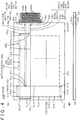
- FIG. 4 to FIG. 8 are diagrams for describing a configuration example of a position detection sensor 20B of the second embodiment.
- the same parts as those of the position detection sensor 20A of the first embodiment will be denoted by the same reference symbols, and a detailed description thereof will be omitted.
- the return wiring path X i Eg of the lead wiring path section 21X i E of the X-axis direction loop coils 21X i formed on the board 23 as described above is combined with the return wiring path X k Eg of the lead wiring path section 21X k E of the other X-axis direction loop coil 21X k (where i ⁇ k) into a common wiring path, reducing the total number of lead wiring paths for connection from the X-axis direction loop coil group 21 to the connector section 24 outside the position detection area 25.
- This ensures reduced concentration and imbalance of the wiring path patterns caused by the existence of the lead wiring paths other than the lead wiring paths of the loop sections of the loop coils in the position detection area 25 as compared to the first embodiment.
- the return wiring paths thereof are connected together to a conductor pattern 26B described later that is formed on the one face 23a of the board 23. The reason for this is to ensure that the conductor pattern 26B formed on the one face 23a of the connector section 24 can serve as a terminal conductor of the reference potential.
- FIG. 4 depicts diagrams for describing an outline of a configuration example of the position detection sensor 20B of the second embodiment and is equivalent to FIG. 1 of the first embodiment.
- the solid straight lines in FIG. 4 to FIG. 8 represent the wiring paths formed on the one face 23a of the board 23, and the dotted straight lines represent the wiring paths formed on the other face 23b of the board 23 as in FIG. 1 .
- a conductor pattern 26B is formed on one face 23a of the board 23, and the return wiring path X i Eg of the lead wiring path section 21X i E of the X-axis direction loop coil 21X i disposed on the other face 23b of the board 23 and the return wiring path Y j Eg of the lead wiring path section 22Y j E of the Y-axis direction loop coil 22Y j are connected via through holes 33X and 33Y to wiring paths 34X and 34Y on the one face 23a of the board 23 near the connector section 24.
- the wiring paths 34X and 34Y are connected together to the one face 23a of the connector section 24 of the board 23.
- the position detection sensor 20B of the second embodiment is similar to the position detection sensor 20A of the first embodiment in other configuration.
- the void holes of the conductor pattern 26B are arranged side by side in the Y-axis direction, and these columns of the void holes running in the Y-axis direction are arranged out of alignment with the adjacent columns of the void holes.
- This arrangement is equal to the formation of void holes 26Bh in the slit area in the dummy conductor pattern 26 of the first embodiment, and wiring path patterns 26Ba are substantially formed in the Y-axis direction in the conductor pattern 26B. It should be noted that although dotted lines are depicted in the conductor pattern 26B in FIG. 4 for easy understanding of the wiring patterns 26Ba, these dotted lines do not actually exist.
- FIG. 5 is a diagram for describing the combination, into a common return wiring path, of any two X-axis loop coils out of the X-axis loop coil group 21 formed on the board 23 of the position detection sensor 20B of the second embodiment, and FIG. 5 illustrates a case in which the lead wiring path section 21X i E of the X-axis direction loop coils 21X i and the lead wiring path section 21X k E of the X-axis direction loop coil 21X k into a return wiring path.
- the solid straight lines represent the wiring paths formed on the one face 23a of the board 23, and the dotted straight lines represent the wiring paths formed on the other face 23b of the board 23 as in FIG. 1 .
- the straight line portions X i La and X i Lb of the loop section 21X i L of the X-axis direction loop coil 21X i formed on the one face 23a of the board 23 are connected to the straight line portions X i Lc and X i Ld formed on the other face 23b of the board 23 via the through holes 31a i , 31b i , 31c i , and 31d i .
- straight line portions X k La and X k Lb of a loop section 21X k L of the X-axis direction loop coil 21X k formed on the one face 23a of the board 23 are connected to straight line portions X k Lc and X k Ld formed on the other face 23b of the board 23 via through holes 31a k , 31b k , 31c k , and 31d k .
- the one end portions of the cut portions of the loop section 21X i L of the X-axis direction loop coil 21X i formed on the one face 23a of the board 23 and the straight line portions X i Lb and X k Lb of the loop section 21X k L of the X-axis direction loop coil 21X k are connected respectively to the outgoing wiring paths X i Es and X k Es of the lead wiring path sections 21X i E and 21X k E via the through holes 31e i and 31e k .
- the other end portions of the cut portions of the straight line portions X i Lb and X k Lb are connected respectively to the return wiring paths X i Eg and X k Eg of the lead wiring path section 21X i E and the lead wiring path section 21X k E via through holes 31f i and 31f k .
- the wiring portion of the return wiring path X i Eg of the lead wiring path section 21X i E of the X-axis direction loop coil 21X i other than between the through holes 31f k and 31f i connected to the through hole 31f k is shared for use as the return wiring path X k Eg of the X-axis direction loop coil 21X k . That is, the return wiring path X i Eg and the return wiring path X k Eg are configured as a common return wiring path CMg.
- the outgoing wiring path XiEs of the lead wiring path section 21X i E of the X-axis direction loop coil 21X i is disposed in parallel and in proximity to the common return wiring path CMg
- the outgoing wiring path X k Es of the lead wiring path section 21X k E of the X-axis direction loop coil 21X k is also disposed in parallel and in proximity to the common return wiring path CMg.
- the common return wiring path CMg is connected to the wiring path 34X on the side of the one face 23a from the side of the other face 23b of the board 23 via the through hole 33X in the region between the position detection area 25 and the connector section 24 outside the position detection area 25.
- the common return wiring path CMg is connected to the conductor pattern 26B on the one face 23a of the connector section 24.
- a return wiring path running in the X-axis direction is combined with other return wiring path running in the X-axis direction into a single wiring path. This ensures that only three lead wiring paths, one less than in related arts, are required as compared to a total of four lead wiring paths required in related arts, two as the lead wiring path section 21X i E of the X-axis direction loop coil 21X i and two as the lead wiring path section 21X k E of the X-axis direction loop coil 21X k .
- the outgoing wiring path X i Es of the lead wiring path section 21X i E of the X-axis direction loop coil 21X i and the outgoing wiring path X k Es of the lead wiring path section 21X k E of the X-axis direction loop coil 21X k are formed on the sides of the common return wiring path CMg.
- the through holes 31e i and 31e k are formed at positions straddling the common return wiring path CMg.
- Disposing the outgoing wiring path X i Es and the outgoing wiring path X k Es on the sides of the common return wiring path CMg as described above ensures that the spacing between the outgoing wiring path X i Es and the common return wiring path CMg and the spacing between the outgoing wiring path X k Es and the common return wiring path CMg are equal, and that the two spacings are, for example, 0.1 mm. This keeps an area portion formed by the outgoing wiring path and the return wiring path to a minimum, making it possible to keep the occurrence of an error signal to a minimum.
- the n X-axis direction loop coils 21X 1 to 21X n of the X-axis direction loop coil group 21 are divided into a plurality of groups G1, G2, and so on, each of which consists of two or more loop coils, so as to combine the return wiring paths into a common wiring path for each group.
- This makes it possible to reduce the total number of return wiring paths of the lead wiring paths drawn out from the X-axis direction loop coil group 21 to the number of these groups. That is, as illustrated in FIG. 6 , it is possible to configure the groups G1, G2, and so on such that one of common return wiring paths CMg1, CMg2, and so on is provided for each group.
- the numbers of X-axis direction loop coils making up the groups G1, G2, and so on need not be the same and may be different.
- the second embodiment permits reduction of the number of lead wiring paths as compared to related arts by combining the return wiring path of an X-axis direction loop coil with the return wiring path of other X-axis direction loop coil into a common wiring path.
- the return wiring paths of the X-axis direction loop coils and the Y-axis direction loop coils are provided on the one face 23a of the board 23, the side opposite to the other face 23b of the board 23 where the outgoing wiring paths are formed and connected to the conductor pattern 26B in the connector section 24, making it possible to downsize the connector section 24 as compared to the first embodiment.
- wiring path patterns running in the directions orthogonal to each other are formed on the one face and the other face of the board 23 including in the connector section 24. Even in the event of shrinkage of the copper paste binder caused by a thermal treatment, shrinkage takes place evenly across the entire board as in the above embodiment. This ensures freedom from partial warping or undulation in the board 23.
- the dummy conductor pattern 26B of the connector section 24 is not a filled pattern that matches with the entire region of the wiring path patterns on the side of the other face 23b of the board 23. Instead, the dummy conductor pattern 26B has a number of void holes 26Bh, making it possible to avoid attenuation of magnetic fluxes which would occur in the case of a filled pattern due to generation of eddy currents in electromagnetic coupling with the position pointer near the filled pattern.
- the dummy conductor pattern 26B is configured in the connector section 24 as a terminal to be connected to a reference potential.
- the one or plurality of common return wiring paths of the lead wiring path section 21X i E from the X-axis direction loop coils 21X i or the one or plurality of return wiring paths of the lead wiring path section 22Y j E from the Y-axis direction loop coils 22Y j may be drawn out onto the other face 23b of the connector section 24 and connected to the dummy conductor pattern 26 via a through hole so that the return wiring paths drawn out onto the other face 23b of the connector section 24 are used as terminals to be connected to a reference potential.
- all return wiring paths X l Eg to X n Eg of the lead wiring path sections 21X 1 E to 21X n E of the n X-axis direction loop coils 21X 1 to 21X n may be naturally combined into the single common return wiring path CMg.
- the second embodiment was described only in relation to the X-axis direction loop coil group 21, the second embodiment is applicable to the Y-axis direction loop coil group 22 in completely the same manner.
- the minimum number of the return wiring paths of the lead wiring path sections can be reduced to two, one for the X-axis direction loop coil group 21 and one for the Y-axis direction loop coil group 22.
- a position detection sensor 20C of a third embodiment is a modification example of the position detection sensor 20B of the second embodiment.
- FIG. 7 and FIG. 8 are diagrams for describing a configuration example of the position detection sensor 20C of the third embodiment.
- the same parts as those of the position detection sensor 20B of the second embodiment will be denoted by the same reference symbols, and a detailed description thereof will be omitted.
- the return wiring path X i Eg of the lead wiring path section 21X i E of the X-axis direction loop coil 21X i is combined with the one straight line portion Y j Lb of the loop section 22Y j L of the Y-axis direction loop coil 22Y j into a common wiring path by connecting the return wiring path X i Eg to the straight line portion Y j Lb for use as part of the straight line portion Y j Lb, further reducing the total number of lead wiring paths for connection from the X-axis direction loop coil group 21 to the connector section 24 outside the position detection area 25.
- This ensures reduced concentration and imbalance of the wiring path patterns caused by the existence of the lead wiring paths other than the lead wiring paths of the loop sections of the loop coils in the position detection area 25 as compared to the first embodiment and the second embodiment.
- the solid straight lines in FIG. 7 represent the wiring paths formed on the one face 23a of the board 23, and the dotted straight lines represent the wiring paths formed on the other face 23b of the board 23 as in FIG. 1 .
- the loop section 22Y j L of the Y-axis direction loop coil 22Y j is formed as a result of connection of the straight line portions Y j La and Y j Lb running in the X-axis direction on the side of the other face 23b of the board and the straight line portions Y j Lc and Y j Ld running in the Y-axis direction on the side of the one face 23a via the through holes 32a j , 32b j , and 32c j .
- the straight line portion Y j Lc on the one face 23a of the board 23 is connected, via the through hole 32d j , to the outgoing wiring path Y j Es formed outside the position detection area 25 in parallel to the X-axis direction on the other face 23b of the board 23.
- the straight line portion Y j Lb running in the X-axis direction formed on the side of the other face 23b of the board 23 is further extended in the X-axis direction outside the position detection area 25 and serves as the return wiring path Y j Eg.
- the loop section 21X i L of the X-axis direction loop coil 21X i is formed as a result of connection of the straight line portions X i La and X i Lb on the side of the one face 23a of the board 23 and the straight line portions X i Lc and X i Ld on the side of the other face 23b via the through holes 31a i , 31b i , 31c i , and 31d i as in FIG. 5 .
- the one end portion of the cut portion of the straight line portion X i Lb formed on the one face 23a of the board 23 is connected, via the through hole 31e i , to the outgoing wiring path X i Es of the lead wiring path section 21X i E formed on the side of the other face 23b of the board 23.
- the outgoing wiring path X i Es is disposed in parallel and in proximity to the straight line portion Y j Lb of the loop section 22Y j L of the Y-axis direction loop coil 22Y j .
- the other end portion of the cut portion of the straight line portion X i Lb is connected, via the through hole 31f i , to an intermediate portion of the straight line portion Y j Lb of the loop section 22Y j L of the Y-axis direction loop coil 22Y j .
- the straight line portion Y j Lb of the loop section 22Y j L is a wiring path whose extended portion serves as the return wiring path Y j Eg of the lead wiring path section 22Y j E of the Y-axis direction loop coil 22Y j as described earlier.
- the straight line portion Y j Lb of the loop section 22Y j L of the Y-axis direction loop coil 22Y j is disposed in parallel and in proximity to the outgoing wiring path X i Es of the lead wiring path section 21X i E of the X-axis direction loop coil 21X i .
- the part of the straight line portion Y j Lb of the loop section 22Y j L of the Y-axis direction loop coil 22Y j from a connection point with the straight line portion X i Lb of the X-axis direction loop coil 21X i via the through hole 31f i to the connector section 24 is shared as the return wiring path X i Eg of the lead wiring path section 21X i E of the X-axis direction loop coil 21X i .
- the lead wiring path section 21X i E of the X-axis direction loop coil 21X i and the lead wiring path section 22Y j E of the Y-axis direction loop coils 22Y j for connection from the position detection area 25 to the connector section 24 (not depicted in FIG. 7 ) outside the position detection area 25 are configured to have a common return wiring path CMYg.
- the common return wiring path CMYg is connected from the other face 23b of the board 23 to the one face 23a via a through hole 33YC and is connected to the conductor pattern 26B illustrated in FIG. 4 via a wiring path 34YC.
- the third embodiment it is no longer necessary to provide an individual return wiring path for the lead wiring path section 21X i E from the X-axis direction loop coils 21X i , making it possible to reduce the number of lead wiring paths by the equal number.
- the number of return wiring paths of the lead wiring path sections from the X-axis direction loop coil group 21 and the Y-axis direction loop coil group 22 as a whole can be reduced to the equal number of the Y-axis direction loop coils. Therefore, it is possible to reduce the number of return wiring paths of the lead wiring path sections from the X-axis direction loop coil group 21 and the Y-axis direction loop coil group 22 as a whole even further as compared to the second embodiment.
- FIG. 8 illustrates a case in which the third embodiment is applied to the example of the second embodiment depicted in FIG. 6 .
- return wiring paths of the X-axis direction loop coils 21X 1 to 21X 6 of the group G1 are shared with some of loop sections 22Y u L of Y-axis direction loop coils 22Y u and drawn out of the position detection area 25 as a common return wiring path CMYg1.
- return wiring paths of the X-axis direction loop coils 21X 7 to 21X 12 of the group G2 are shared with some of loop sections 22Y v L of the Y-axis direction loop coils 22Y v and drawn out of the position detection area 25 as a common return wiring path CMYg2.
- connector section 24 is provided on one side in the X-axis direction of the board 23, a connector section may be provided on one side in the Y-axis direction of the board 23.
- the method by which wiring path patterns are substantially formed in the conductor pattern 26 or 26B provided in the connector section 24 is not limited to the method, as above embodiment, in which slits are provided or void holes are provided. Instead, any method may be used as long as wiring path patterns orthogonal to extended portions of the lead wiring paths formed on the side of the other face of the connector section 24 can be substantially formed.
- a conductor pattern 26C illustrated in FIG. 9(A) is formed as a so-called zigzag wiring path pattern with each of a plurality of wiring path patterns 26Ca connected alternately at one or other end portion of the respective wiring path patterns 26Ca.
- a conductor pattern 26D illustrated in FIG. 9(B) is a pattern in which a plurality of wiring path patterns 26Da are coupled only at their one end portions. In FIG. 9(B) , it is needless to say that areas where the plurality of wiring path patterns 26Da are coupled may be located on the side of other end portions of the plurality of wiring path patterns 26Da.
- a conductor pattern 26E illustrated in FIG. 9(C) is a pattern in which a plurality of wiring path patterns 26Ea are coupled individually at center portions of the respective wiring path patterns 26Ea.
- the conductor patterns 26C, 26D, and 26E are terminals that can supply a reference potential. If it is not necessary to use the conductor patterns 26C, 26D, and 26E as terminals for supplying a reference potential, as described in the first embodiment, the conductor patterns 26Ca, 26Da, and 26Ea may be wiring path patterns (dummy patterns) that are independent of each other as described earlier.
Landscapes
- Engineering & Computer Science (AREA)
- Physics & Mathematics (AREA)
- General Engineering & Computer Science (AREA)
- Theoretical Computer Science (AREA)
- General Physics & Mathematics (AREA)
- Human Computer Interaction (AREA)
- Electromagnetism (AREA)
- Manufacturing & Machinery (AREA)
- Microelectronics & Electronic Packaging (AREA)
- Computer Networks & Wireless Communication (AREA)
- Measurement Of Length, Angles, Or The Like Using Electric Or Magnetic Means (AREA)
- Transmission And Conversion Of Sensor Element Output (AREA)
Abstract
Description
- The present invention relates to an electromagnetic induction position detection sensor.
- An electromagnetic induction position detection sensor is formed by a number of loop coils disposed in X-axis and Y-axis directions of coordinate axes on a board. A position detection device having a position detection sensor permits detection of coordinates of a position pointed to by a position pointer in the X-axis and Y-axis directions based on electromagnetic induction action between the position pointer and the position detection sensor.
- Conventional position detection sensors were fabricated by etching copper on an epoxy resin board. Recent years have seen use of position detection devices in compact portable terminals. For this reason, position detection sensors have also been required to be more compact and lighter in weight. Therefore, screen-printed position detection sensors using metal paste that are lower in cost than etched ones and that can be volume-produced have come into use.
- Metal paste used not only for position detection sensors but also for ordinary circuit boards includes metallic powder and a resin binder (bonding agent). Then, metal paste applied to the circuit board is subjected to a thermal treatment so that conductivity is enhanced by fusing the metal powder to each other.
- Heat-resistant polyimide-based resin sheet is used as a board material on which to screen-print a metal paste. Also, a metal, particularly used as a metal powder of metal paste, is silver. A position detection sensor having a board coated with silver paste through screen printing offers high conductivity and can be fabricated by heating at approximately 200°C to 250°C, relatively low temperatures for a thermal treatment, for approximately 20 to 30 minutes, and, therefore, has become popular.
- However, fabricating a position detection sensor using silver paste had the following problems. First, silver paste was expensive, resulting in higher cost than conventional copper etching. Also, in order to achieve downsizing while at the same time maintaining the number of loop coils of the position detection sensor in today's compact portable terminals against the backdrop of demands for more compact terminals, it is necessary to reduce a loop coil width and a spacing between the loop coils to the extent possible. However, if silver paste is used, the coil spacing cannot be reduced due to ion migration phenomenon. This has led to a problem characterized by difficulties in fabricating compact position detection sensors using silver paste.
- For this reason, use of copper paste using copper powder that is cheaper and free from ion migration phenomenon has been proposed in place of silver (refer to Patent Document 1 (
WO2012/157704 )). - As described in
Patent Document 1, however, copper powder has a drawback in that it is prone to formation of an oxide film on the surface and its conductivity degrades due to an oxide layer. In the case of copper in particular, conventional temperatures and heating time result in formation of an oxide film. For this reason, forming loop coils on a sheet-shaped board using copper paste requires a reduction process at temperatures beyond 300°C, temperatures higher than for silver paste, to reduce the oxide film of copper powder, a sintering process at higher temperature, and a short-time thermal treatment to provide resistance to formation of an oxide film. - However, if loop coils are formed on a sheet-shaped board made of polyimide-based resin using copper paste under such high temperatures, a binder included in the copper paste shrinks, leading to shrinkage of paste wiring itself made of copper paste. This shrinkage exerts a shrinking force on the sheet-shaped board, causing problems including warping and undulation on the sheet-shaped board depending on the location. In the event of such warping or undulation, the size of the position detection sensor itself changes, rendering it impossible to detect positions with accuracy.
- As a method for reducing this warping caused by shrinkage, a method is proposed in Patent Document 2 (Japanese Patent Laid-Open No.
Hei 9-55568 -
- Patent Document 1:
WO2012/157704 - Patent Document 2: Japanese Patent Laid-Open No.
Hei 9-55568 - However, there was a problem with applying the method of
Patent Document 2 in an 'as-is' fashion to a position detection sensor. That is, wiring is printed on both faces to eliminate warping of the board. However, if there is an imbalance in wiring between one face the other face, wrinkles and undulations occur. - For example, as depicted in
FIG. 10(A) , no problem arose ifwiring paths 2 made of copper paste were successfully formed, one on one face 1a and another on anotherface 1b, at positions opposed to each other on a sheet-shaped board 1. However, as depicted inFIG. 10(B) , in the event of an unevenness between positions of thewiring paths 2 due to misalignment from the opposing positions, the binder shrank, causing an undulation problem as depicted inFIG. 10(C) . - Then, a position detection sensor has areas where wiring is partially concentrated and areas where wiring is distributed unevenly in one direction such as a connector section between the position detection sensor and a position detection circuit. In such areas, wrinkle and undulation problems occurred despite wiring printed on both faces using the method described in
Patent Document 2. - It is an object of the present invention to provide an electromagnetic induction position detection sensor that can solve the above problems.
- In order to solve the above problems, the invention of
claim 1 provides an electromagnetic induction position detection sensor that has a wiring path pattern made of copper paste that includes copper powder and a binder formed on a sheet-shaped board made of resin and that has a plurality of position detection loop coils formed by thermally treating the wiring path pattern. The wiring path pattern is configured to include the position detection loop coils and a connector section for connection between the position detection loop coils and external circuitry. On one face of the sheet-shaped board, the wiring path pattern made of the copper paste is formed to extend in a first direction, and the wiring path pattern formed to extend in the first direction is formed to extend in a second direction orthogonal to the first direction at a given pitch. On another face of the sheet-shaped board, the wiring path pattern made of the copper paste is formed to extend in the second direction, and the wiring path pattern formed to extend in the second direction is formed to extend in the first direction at a given pitch. Further, a wiring path pattern is disposed on the one face and the other face in the connector section. - In the electromagnetic induction position detection sensor of
claim 1 configured as described above, the plurality of wiring patterns formed to extend in the first direction on the one face of the sheet-shaped board are formed in the second direction at the given pitch, and the plurality of wiring patterns formed to extend in the second direction on the other face of the sheet-shaped board are formed in the first direction at the given pitch. Therefore, the plurality of wiring path patterns made of the copper paste are formed in the directions orthogonal to each other on the one face and the other face of the sheet-shaped board. - Then, the plurality of wiring patterns formed on both faces of the sheet-shaped board are each formed at the given pitch. As a result, lattices of a given size are formed evenly approximately across the entire sheet-shaped board thanks to the plurality of wiring path patterns on both faces of the sheet-shaped board. Therefore, even in the event of shrinkage of the copper paste binder due to thermal treatment, that shrinkage takes place evenly approximately across the entire sheet-shaped board, ensuring freedom from partial warping or undulation. This makes it possible to provide a position detection sensor that offers high accuracy even when copper paste is used.
- Also, the invention of
claim 2 is characterized in that, in the invention ofclaim 1, the connector section is provided, at a given end portion of the sheet-shaped board, in which extended portions of lead wiring paths from a loop section of the position detection loop coils are formed. Wiring path patterns in the directions orthogonal to each other are also substantially formed on the one face and the other face of the sheet-shaped board in the connector section. - In the electromagnetic induction position detection sensor according to
claim 2 of the invention, patterns made of the copper paste are also substantially formed in the directions orthogonal to each other on one face and another face of the connector section. Therefore, in the connector section, even in the event of shrinkage of the copper paste binder in the wiring path patterns orthogonal to each other, the connector section as a whole shrinks evenly, preventing warping or undulation of the connector section. - The electromagnetic induction position detection sensor according to the present invention has an effect in that if loop coils are formed on a sheet-shaped board made of a polyimide-based resin using copper paste, and even in the event of shrinkage of a binder included in the copper paste by a thermal treatment, that shrinkage takes place evenly approximately across the entire sheet-shaped board, and as a result, the sheet-shaped board is kept free from partial warping or undulation. The position detection sensor also has an effect in that accuracy can be maintained.
-
- [
FIG. 1 ]
FIG. 1 depicts diagrams illustrating a configuration example of a first embodiment of a position detection sensor according to the present invention. - [
FIG. 2 ]
FIG. 2 is a block diagram for describing a position detection circuit of a coordinate input device using an embodiment of the position detection sensor according to the present invention. - [
FIG. 3 ]
FIG. 3 is a diagram used to describe a configuration example of the first embodiment of the position detection sensor according to the present invention. - [
FIG. 4 ]
FIG. 4 depicts diagrams illustrating a configuration example of a second embodiment of the position detection sensor according to the present invention. - [
FIG. 5 ]
FIG. 5 is a diagram for describing main parts of the configuration example of the second embodiment of the position detection sensor according to the present invention. - [
FIG. 6 ]
FIG. 6 is a diagram for describing main parts of the configuration example of the second embodiment of the position detection sensor according to the present invention. - [
FIG. 7 ]
FIG. 7 is a diagram for describing main parts of a configuration example of a third embodiment of the position detection sensor according to the present invention. - [
FIG. 8 ]
FIG. 8 is a diagram for describing main parts of the configuration example of the third embodiment of the position detection sensor according to the present invention. - [
FIG. 9 ]
FIG. 9 depicts diagrams for describing other example of some of the configuration examples of the position detection sensor according to the present invention. - [
FIG. 10 ]
FIG. 10 depicts diagrams for describing technical challenges to be solved of the position detection sensor according to the present invention. - A description will be given below of embodiments of an electromagnetic induction position detection sensor according to the present invention with reference to drawings.
- First, before describing a first embodiment of the position detection sensor according to the present invention, a configuration example of an electromagnetic induction coordinate input device using the position detection sensor of embodiments of the present invention described below will be described with reference to
FIG. 2 . A pen-type position pointer 300 used together with an electromagnetic induction coordinateinput device 200 in this example incorporates a parallel resonance circuit that includes acoil 301 and acapacitor 302 connected in parallel to thecoil 301 as illustrated inFIG. 2 . - In a
position detection sensor 20 of the coordinateinput device 200 in this example, aloop coil group 21 running in the X-axis direction and a loop coil group 22 running in the Y-axis direction are disposed on each of top and rear faces of a sheet-shapedboard 23 made of polyimide-based resin in such a manner as to spatially overlap each other as illustrated inFIG. 2 . It should be noted that in the example described below the direction across the board of theposition detection sensor 20 is assumed to be the X-axis direction, and the direction down the board of theposition detection sensor 20 is assumed to be the Y-axis direction. - In the case of this example, as depicted in
FIG. 2 , theloop coil group 21 running in the X-axis direction includes n (where n is an integer equal to 2 or more) rectangular loop coils 21X1 to 21Xn that are arranged at a given pitch in the X-axis direction, and the loop coil group 22 running in the Y-axis direction includes m (where m is an integer equal to 2 or more) loop coils 22Y1 to 22Ym that are arranged at a given pitch in the Y-axis direction. In theposition detection sensor 20, aposition detection area 25 includes a loop section of theloop coil group 21 running in the X-axis direction and a loop section of the loop coil group 22 running in the Y-axis direction. - Two wiring paths are led out from each of the loop section of the
loop coil group 21 running in the X-axis direction and the loop section of the loop coil group 22 running in the Y-axis direction as described earlier. Each one of the wiring paths (return wiring path which will be described later) is connected to each other as illustrated inFIG. 2 and connected to a terminal supplied with a reference potential, a ground terminal in the example depicted inFIG. 2 . - The
position detection sensor 20 is connected to aposition detection circuit 210 via a connector section that is omitted in the figure. Theposition detection circuit 210 includes aselection circuit 211, anoscillator 212, acurrent driver 213, a transmission/reception switching circuit 214, a receivingamplifier 215, adetection circuit 216, a low-pass filter 217, a sample-hold circuit 218, an analog to digital (A/D)conversion circuit 219, and aprocessing control section 220. - The X-axis direction
loop coil group 21 and the Y-axis direction loop coil group 22 are connected by theselection circuit 211. Theselection circuit 211 successively selects one of the loop coils of the twoloop coil groups 21 and 22 in accordance with a control instruction from theprocessing control section 220. - The
oscillator 212 generates an alternate current (AC) signal at a frequency f0. This AC signal is supplied to thecurrent driver 213 for conversion into a current and then sent to the transmission/reception switching circuit 214. The transmission/reception switching circuit 214 switches, every given time period, between connection destinations (transmitting side terminal T and receiving side terminal R) to which the loop coil selected by theselection circuit 211 is connected under control of theprocessing control section 220. Thecurrent driver 213 is connected to the transmitting side terminal T, and the receivingamplifier 215 is connected to the receiving side terminal R. - During transmission, therefore, the AC signal from the
current driver 213 is supplied to the loop coil selected by theselection circuit 211 via the transmitting side terminal T of the transmission/reception switching circuit 214. During reception, on the other hand, the induced voltage generated in the loop coil selected by theselection circuit 211 is supplied to the receivingamplifier 215 via theselection circuit 211 and the receiving side terminal R of the transmission/reception switching circuit 214 for amplification and sent to thedetection circuit 216. - The signal detected by the
detection circuit 216 is supplied to the A/D conversion circuit 219 via the low-pass filter 217 and the sample-hold circuit 218. The A/D conversion circuit 219 converts the analog signal into a digital signal and supplies the signal to theprocessing control section 220. - The
processing control section 220 performs control for position detection. That is, theprocessing control section 220 controls loop coil selection by theselection circuit 211, signal switching by the transmission/reception switching circuit 214, timings of the sample-hold circuit 218, and so on. - The
processing control section 220 controls energization of the loop coil selected by theselection circuit 211 of the X-axis directionloop coil group 21 or the Y-axis direction loop coil group 22 to send electromagnetic waves by switching the transmission/reception switching circuit 214 for connection to the transmitting side terminal T. The resonance circuit of theposition pointer 300 receives electromagnetic waves sent from this loop coil and stores energy. - Next, the
processing control section 220 switches the transmission/reception switching circuit 214 for connection to the receiving side terminal R. Then, an induced voltage is generated in each of the loop coils of the X-axis directionloop coil group 21 and the Y-axis direction loop coil group 22 by electromagnetic waves sent from theposition pointer 300. Theprocessing control section 220 calculates coordinate values of the position pointed to in the X-axis and Y-axis directions in aposition detection area 25 of theposition detection sensor 20 based on the voltage level of the induced voltage generated in each of the loop coils. Then, theprocessing control section 220 supplies calculated coordinate value information, for example, to an external personal computer. -
FIG. 1 depicts diagrams for describing a position detection sensor 20A of the first embodiment applied to theposition detection sensor 20 illustrated inFIG. 2 . This drawing is intended to describe how each ofloop coils 21Xi (where i is any one of 1, 2 and so on up to n) of the X-axis directionloop coil group 21 and each of loop coils 22Yj (where j is any one of 1, 2 and so on up to m) of the Y-axis direction loop coil group 22 are formed with respect to the sheet-shapedboard 23. -
FIG. 1(A) is a view as seen from the side of oneface 23a of theboard 23, andFIG. 1(B) is a view as seen from a direction vertical to theface 23a of theboard 23. InFIG. 1(B) , illustration of a conductor pattern making up the loop coils 21Xi and 22Yj is omitted. - As illustrated in
FIGS. 1(A) and 1(B) and as described earlier, the sheet-shapedboard 23 in this example is a thin film-shaped flexible board made of polyimide-based resin. Then, straight line portions XiLa and XiLb parallel to the Y-axis direction of aloop section 21XiL shaped to surround a rectangular area of the X-axisdirection loop coil 21Xi are formed on the side of the oneface 23a of the sheet-shapedboard 23 - (hereinafter referred to as the board 23), and straight line portions XiLc and XiLd parallel to the X-axis direction to connect the straight line portions XiLa and XiLb of the
loop section 21XiL are formed on the side of theother face 23b of theboard 23. The straight line portions XiLa and XiLb on the side of the oneface 23a of theboard 23 are connected to the straight line portions XiLc and XiLd on the side of theother face 23b via throughholes - Then, one of the straight line portions XiLa and XiLb of the
loop section 21XiL provided on the side of the oneface 23a of theboard 23, which is the straight line portion XiLb in the case ofFIG. 1 , is cut in the middle for connection to a leadwiring path section 21XiE that includes first and second wiring paths that are parallel to each other. - One of the first and second wiring paths making up the lead
wiring path section 21XiE is connected to theselection circuit 211 of theposition detection circuit 210 described earlier via theconnector section 24 and serves as a wiring path to which a signal is supplied or from which a signal is extracted. This wiring path to which a signal is supplied or from which a signal is extracted will be hereinafter referred to as an outgoing wiring path. On the other hand, the other of the first and second wiring paths making up the leadwiring path section 21XiE is a wiring path connected to a reference potential such as ground potential. This wiring path connected to a reference potential such as ground potential will be hereinafter referred to as a return wiring path. - One end portion of a cut portion of the straight line portion XiLb of the
loop section 21XiL of the X-axisdirection loop coil 21Xi is connected, via a throughhole 31ei, to an outgoing wiring path XiEs of the leadwiring path section 21XiE formed on the side of theother face 23b of theboard 23, and other end portion of the cut portion of the straight line portion XiLb is connected, via a throughhole 31fi, to a return wiring path XiEg of the leadwiring path section 21XiE formed on the side of theother face 23b of theboard 23. The outgoing wiring path XiEs and the return wiring path XiEg are disposed in parallel and in proximity to each other as straight lines in the X-axis direction in this example. - As illustrated in
FIG. 1 , the leadwiring path section 21XiE of the X-axisdirection loop coil 21Xi also exists in theposition detection area 25 in this example. At least, the outgoing wiring path XiEs and the return wiring path XiEg of the leadwiring path section 21XiE in theposition detection area 25 are disposed as straight lines that run in proximity and in parallel to each other in the X-axis direction. A spacing between the outgoing wiring path XiEs and the return wiring path XiEg is, for example, 0.1 mm. - The outgoing wiring path XiEs and the return wiring path XiEg are straight lines that run in proximity and in parallel to each other as described above to keep to a minimum an error signal at the time of position detection by the position detection circuit. The error signal is an unnecessary current produced because of the existence of the lead
wiring path section 21XiE in theposition detection area 25 and as a result of the passage of magnetic fluxes through a thin and narrow surface formed by the pair of straight lines. - Then, in this example, the outgoing wiring path XiEs and the return wiring path XiEg of the lead
wiring path section 21XiE are disposed in such a manner as to extend up to theconnector section 24 provided outside theposition detection area 25 on theother face 23b of theboard 23. - Then, on the
board 23, the plurality of X-axis direction loop coils 21Xi configured as described above are disposed in the X-axis direction at a given pitch with theloop sections 21XiL partially overlapping each other. - Also, straight line portions YjLa and YjLb parallel to the X-axis direction of a
loop section 22YjL shaped to surround a rectangular area of the Y-axisdirection loop coil 22Yj are formed on the side of theother face 23b of theboard 23. Then, straight line portions YjLc and YjLd parallel to the Y-axis direction to connect the straight line portions YjLa and YjLb of theloop section 22YjL are formed on the side of the oneface 23a of theboard 23. The straight line portions YjLa and YjLb on the side of theother face 23b of theboard 23 and the straight line portions YjLc and YjLd on the side of the oneface 23a are connected via throughholes - Then, one of the straight line portions YjLa and YjLb of the
loop section 22YjL of the Y-axisdirection loop coil 22Yj provided on the side of theother face 23b of theboard 23, which is the straight line portion YjLb in the example depicted inFIG. 1 , is extended further outward beyond theposition detection area 25 up to theconnector section 24 in the X-axis direction and serves as a return wiring path YjEg of the leadwiring path section 22YjE. Also, the straight line portion YjLc of theloop section 22YjL located closest to the connector side in the X-axis direction in theposition detection area 25 is connected to an outgoing wiring path YjEs of the leadwiring path section 22YjE formed in the X-axis direction on the side of theother face 23b of theboard 23 via the throughhole 32dj. The outgoing wiring path YjEs is disposed in parallel and in proximity to the return wiring path YjEg and extended up to theconnector section 24. - Then, on the
board 23, the plurality of Y-axis direction loop coils 22Yj configured as described above are disposed in the Y-axis direction at a given pitch with theloop sections 22YjL partially overlapping each other. - As described above, in the position detection sensor 20A, the plurality of X-axis direction loop coils 21Xi and the plurality of Y-axis direction loop coils 22Yj are disposed in the directions orthogonal to each other on the one
face 23a and theother face 23b of theboard 23 in the position detection area of theboard 23. As a result, lattices of a given size are formed evenly approximately across theentire board 23 thanks to the plurality of wiring path patterns of loop coils on both faces of theboard 23. - Then, on the
other face 23b of theconnector section 24, the leadwiring path section 21XiE from the plurality of X-axis direction loop coils 21Xi and the leadwiring path section 22YjE from the plurality of Y-axis direction loop coils 22Yj are formed parallel to each other in such a manner as to be drawn out in the X-axis direction. - In the present embodiment, a
dummy conductor pattern 26 having a plurality of wiring path patterns 26a is formed on the oneface 23a of theconnector section 24 as illustrated inFIG. 1(A) . The wiring path patterns 26a run in a direction orthogonal to the leadwiring path section 21XiE and the leadwiring path section 22YjE in a region opposed to the leadwiring path section 21XiE from the plurality of X-axis direction loop coils 21Xi and the leadwiring path section 22YjE from the plurality of Y-axis direction loop coils 22Yj on the side of theother face 23b. - In the present embodiment, the plurality of wiring path patterns 26a are formed by forming slits in the Y-axis direction in the
dummy conductor pattern 26. It should be noted, however, that, in the present embodiment, the plurality of wiring path patterns 26a are connected to each other at their end portions. - In the position detection sensor 20A of the present embodiment, therefore, wiring path patterns orthogonal to each other are also substantially formed in the
connector section 24 of theboard 23. - The position detection sensor 20A described above is fabricated, for example, by coating the one
face 23a andother face 23b of the sheet-shapedboard 23 with copper paste through screen printing and forming the X-axis loop coil group and the Y-axis loop coil group described above (including the connector sections). Here, copper paste includes copper powder, a solvent, and binder resin. It should be noted that the method described, for example, in Japanese Patent Laid-Open No.2015-35331 - The copper paste coated on the
board 23 is subjected to a superheated steam treatment, reducing the oxidized copper, and changing the copper paste into wiring paths having high electrical conductivity with a specific resistance of 10 Ω.cm or less. In the present embodiment, the superheated steam treatment is conducted for one to two minutes in a temperature range from 320°C to 370°C. Here, the temperature of the superheated steam treatment is determined in consideration of the conductivity (specific resistance) of the copper paste and shrinkage rate that occurs in the polyimide-basedresin board 23. -
FIG. 3 is a diagram illustrating a relationship between the shrinkage rate of theboard 23 with a change in temperature during the superheated steam treatment and the specific resistance of the wiring paths made of copper paste formed on theboard 23. When the specific resistance is large, it is difficult to pass a current through the loop coils, making it difficult for the position detection sensor to conduct detection operation. When the shrinkage rate of theboard 23 is large, the loop coils deform, degrading the coordinate position accuracy of the position detection sensor. - In
FIG. 3 , black circle represents the specific resistance of the wiring paths made of copper paste. Also, triangle represents the shrinkage rate of theboard 23 subjected to the superheated steam treatment for one minute, and cross mark represents the shrinkage rate of theboard 23 subjected to the superheated steam treatment for two minutes. - It is clear from
FIG. 3 that the specific resistance drops to 10 Ω.cm or less at 320°C or more and drops to approximately 6 Ω.cm or less at 370°C or more, and that the specific resistance roughly saturates without diminishing at higher temperatures. It has also become clear that the shrinkage of theboard 23 hardly takes place at 340°C or less and that shrinkage takes place in different amounts from one location to another in a patchy manner at 370°C or more. - For this reason, the temperature of the superheated steam treatment was set to fall in the range from 320°C to 370°C in the present embodiment, and to 340°C particularly in this example with a process time of two minutes. This made it possible to reduce the specific resistance while at the same time keeping the shrinkage of the
board 23 to a minimum. It should be noted that the process time may be naturally one minute. - Then, even if the copper paste binder shrinks due to a thermal treatment at a high temperature such as 340°C, shrinkage takes place evenly approximately across the entire
position detection area 25 of theboard 23 because the position detection sensor 20A of the above embodiment has wiring path patterns running in the directions orthogonal to each other formed in an orderly manner at a given pitch on the one and other faces of theboard 23 in theposition detection area 25. This ensures that theposition detection area 25 is free from partial warping or undulation. - It should be noted that the
position detection circuit 210 connected to the position detection sensor 20A can correct coordinates pointed to by the position pointer obtained from the position detection sensor in accordance with shrinkage that takes place across theentire board 23 of the position detection sensor 20A. Therefore, even if theboard 23 of the position detection sensor 20A shrinks, coordinate accuracy can be maintained high. - Also, in the
connector section 24, the wiring path patterns of the lead wiring path section on the one face and the wiring path patterns 26a of thedummy conductor pattern 26 on the other face similarly run orthogonal to each other. As a result, lattice patterns are also formed evenly in theconnector section 24, ensuring freedom from partial warping or undulation. - Then, the
dummy conductor pattern 26 of theconnector section 24 is not a filled pattern that matches with the entire region of the wiring path patterns on the side of theother face 23b of theboard 23. Instead, thedummy conductor pattern 26 has slits and, therefore, has an effect in that it is possible to avoid attenuation of magnetic fluxes which would occur in the case of a filled pattern due to generation of eddy currents in electromagnetic coupling with the position pointer near the filled pattern. - It should be noted that although the
dummy conductor pattern 26 is configured such that the plurality of wiring path patterns 26a are connected to each other, thedummy conductor pattern 26 may be configured such that each of the plurality of wiring path patterns 26a is independent of other patterns. - Also, although, in the above embodiment, both the outgoing wiring path and the return wiring path of the lead
wiring path section 21XiE from the X-axis direction loop coils 21Xi and the leadwiring path section 22YjE from the Y-axis direction loop coils 22Yj are provided on the side of theother face 23b of theconnector section 24, the return wiring paths of the leadwiring path section 21XiE from the X-axis direction loop coils 21Xi and the leadwiring path section 22YjE from the Y-axis direction loop coils 22Yj may be connected together to thedummy conductor pattern 26 via a through hole near theconnector section 24. - In this case, the
dummy conductor pattern 26 is configured in theconnector section 24 as a terminal to be connected to a reference potential. Alternatively, the one or plurality of return wiring paths of the leadwiring path section 21XiE from the X-axis direction loop coils 21Xi and the leadwiring path section 22YjE from the Y-axis direction loop coils 22Yj may be drawn out onto theother face 23b of theconnector section 24 and connected to thedummy conductor pattern 26 via a through hole so that the return wiring paths drawn out onto theother face 23b of theconnector section 24 may be used as terminals to be connected to a reference potential. - Also, although the
dummy conductor pattern 26 of the above embodiment substantially has a plurality of wiring path patterns thanks to the slits provided, a plurality of wiring path patterns may be substantially provided by forming, rather than the slit area, void holes having a diameter equal to the width of the slits in the slit area. - A position detection sensor of a second embodiment is one of modification examples of the position detection sensor 20A of the first embodiment.
FIG. 4 to FIG. 8 are diagrams for describing a configuration example of aposition detection sensor 20B of the second embodiment. InFIG. 4 to FIG. 8 , the same parts as those of the position detection sensor 20A of the first embodiment will be denoted by the same reference symbols, and a detailed description thereof will be omitted. - In the
position detection sensor 20B of the second embodiment, the return wiring path XiEg of the leadwiring path section 21XiE of the X-axis direction loop coils 21Xi formed on theboard 23 as described above is combined with the return wiring path XkEg of the leadwiring path section 21XkE of the other X-axisdirection loop coil 21Xk (where i≠k) into a common wiring path, reducing the total number of lead wiring paths for connection from the X-axis directionloop coil group 21 to theconnector section 24 outside theposition detection area 25. This ensures reduced concentration and imbalance of the wiring path patterns caused by the existence of the lead wiring paths other than the lead wiring paths of the loop sections of the loop coils in theposition detection area 25 as compared to the first embodiment. - Also, in the second embodiment, although extended portions of the outgoing wiring paths of the lead
wiring path section 21XiE of the X-axis direction loop coils 21Xi and the leadwiring path section 22YjE of the Y-axis direction loop coils 22Yj are formed on theother face 23b of theboard 23, the return wiring paths thereof are connected together to aconductor pattern 26B described later that is formed on the oneface 23a of theboard 23. The reason for this is to ensure that theconductor pattern 26B formed on the oneface 23a of theconnector section 24 can serve as a terminal conductor of the reference potential. -
FIG. 4 depicts diagrams for describing an outline of a configuration example of theposition detection sensor 20B of the second embodiment and is equivalent toFIG. 1 of the first embodiment. It should be noted that the solid straight lines inFIG. 4 to FIG. 8 represent the wiring paths formed on the oneface 23a of theboard 23, and the dotted straight lines represent the wiring paths formed on theother face 23b of theboard 23 as inFIG. 1 . - As illustrated in
FIG. 4 , in theposition detection sensor 20B of the second embodiment, aconductor pattern 26B is formed on oneface 23a of theboard 23, and the return wiring path XiEg of the leadwiring path section 21XiE of the X-axisdirection loop coil 21Xi disposed on theother face 23b of theboard 23 and the return wiring path YjEg of the leadwiring path section 22YjE of the Y-axisdirection loop coil 22Yj are connected via throughholes wiring paths face 23a of theboard 23 near theconnector section 24. Thewiring paths face 23a of theconnector section 24 of theboard 23. Theposition detection sensor 20B of the second embodiment is similar to the position detection sensor 20A of the first embodiment in other configuration. - The void holes of the
conductor pattern 26B are arranged side by side in the Y-axis direction, and these columns of the void holes running in the Y-axis direction are arranged out of alignment with the adjacent columns of the void holes. This arrangement is equal to the formation of void holes 26Bh in the slit area in thedummy conductor pattern 26 of the first embodiment, and wiring path patterns 26Ba are substantially formed in the Y-axis direction in theconductor pattern 26B. It should be noted that although dotted lines are depicted in theconductor pattern 26B inFIG. 4 for easy understanding of the wiring patterns 26Ba, these dotted lines do not actually exist. - A description will be given next of the combination of the return wiring path XiEg of the lead
wiring path section 21XiE of the X-axisdirection loop coil 21Xi and the return wiring path XkEg of the leadwiring path section 21XkE of the otherX-direction loop coil 21Xk (where i≠k) into a common wiring path in theposition detection sensor 20B of the second embodiment. -
FIG. 5 is a diagram for describing the combination, into a common return wiring path, of any two X-axis loop coils out of the X-axisloop coil group 21 formed on theboard 23 of theposition detection sensor 20B of the second embodiment, andFIG. 5 illustrates a case in which the leadwiring path section 21XiE of the X-axis direction loop coils 21Xi and the leadwiring path section 21XkE of the X-axisdirection loop coil 21Xk into a return wiring path. InFIG. 5 , the solid straight lines represent the wiring paths formed on the oneface 23a of theboard 23, and the dotted straight lines represent the wiring paths formed on theother face 23b of theboard 23 as inFIG. 1 . - As described earlier, the straight line portions XiLa and XiLb of the
loop section 21XiL of the X-axisdirection loop coil 21Xi formed on the oneface 23a of theboard 23 are connected to the straight line portions XiLc and XiLd formed on theother face 23b of theboard 23 via the throughholes loop section 21XkL of the X-axisdirection loop coil 21Xk formed on the oneface 23a of theboard 23 are connected to straight line portions XkLc and XkLd formed on theother face 23b of theboard 23 via throughholes - Then, the one end portions of the cut portions of the
loop section 21XiL of the X-axisdirection loop coil 21Xi formed on the oneface 23a of theboard 23 and the straight line portions XiLb and XkLb of theloop section 21XkL of the X-axisdirection loop coil 21Xk are connected respectively to the outgoing wiring paths XiEs and XkEs of the leadwiring path sections 21XiE and 21XkE via the throughholes - Also, the other end portions of the cut portions of the straight line portions XiLb and XkLb are connected respectively to the return wiring paths XiEg and XkEg of the lead
wiring path section 21XiE and the leadwiring path section 21XkE via throughholes wiring path section 21XiE of the X-axisdirection loop coil 21Xi other than between the throughholes hole 31fk is shared for use as the return wiring path XkEg of the X-axisdirection loop coil 21Xk. That is, the return wiring path XiEg and the return wiring path XkEg are configured as a common return wiring path CMg. - Then, the outgoing wiring path XiEs of the lead
wiring path section 21XiE of the X-axisdirection loop coil 21Xi is disposed in parallel and in proximity to the common return wiring path CMg, and the outgoing wiring path XkEs of the leadwiring path section 21XkE of the X-axisdirection loop coil 21Xk is also disposed in parallel and in proximity to the common return wiring path CMg. - Then, as illustrated in
FIG. 5 , in theposition detection sensor 20B of the second embodiment, the common return wiring path CMg is connected to thewiring path 34X on the side of the oneface 23a from the side of theother face 23b of theboard 23 via the throughhole 33X in the region between theposition detection area 25 and theconnector section 24 outside theposition detection area 25. As a result, the common return wiring path CMg is connected to theconductor pattern 26B on the oneface 23a of theconnector section 24. - As described above, in the second embodiment, a return wiring path running in the X-axis direction is combined with other return wiring path running in the X-axis direction into a single wiring path. This ensures that only three lead wiring paths, one less than in related arts, are required as compared to a total of four lead wiring paths required in related arts, two as the lead
wiring path section 21XiE of the X-axisdirection loop coil 21Xi and two as the leadwiring path section 21XkE of the X-axisdirection loop coil 21Xk. - Then, in the first embodiment, further, the outgoing wiring path XiEs of the lead
wiring path section 21XiE of the X-axisdirection loop coil 21Xi and the outgoing wiring path XkEs of the leadwiring path section 21XkE of the X-axisdirection loop coil 21Xk are formed on the sides of the common return wiring path CMg. For this reason, the throughholes - Disposing the outgoing wiring path XiEs and the outgoing wiring path XkEs on the sides of the common return wiring path CMg as described above ensures that the spacing between the outgoing wiring path XiEs and the common return wiring path CMg and the spacing between the outgoing wiring path XkEs and the common return wiring path CMg are equal, and that the two spacings are, for example, 0.1 mm. This keeps an area portion formed by the outgoing wiring path and the return wiring path to a minimum, making it possible to keep the occurrence of an error signal to a minimum.
- As described above, it is possible to reduce the total number of return wiring paths of the lead wiring paths drawn out from the X-axis direction
loop coil group 21 to half of what it was for each two loop coils of the n loop coils 21Xi to 21Xn of the X-axis directionloop coil group 21 by combining the return wiring paths of the leadwiring path sections 21XiE to 21XnE into a common wiring path. - Further, it is possible to reduce the total number of return wiring paths of the lead wiring paths drawn out from the X-axis direction
loop coil group 21 to an even smaller number by combining the return wiring paths of three or more X-axis direction loop coils into a common wiring path. - For example, as illustrated in
FIG. 6 , the n X-axis direction loop coils 21X1 to 21Xn of the X-axis directionloop coil group 21 are divided into a plurality of groups G1, G2, and so on, each of which consists of two or more loop coils, so as to combine the return wiring paths into a common wiring path for each group. This makes it possible to reduce the total number of return wiring paths of the lead wiring paths drawn out from the X-axis directionloop coil group 21 to the number of these groups. That is, as illustrated inFIG. 6 , it is possible to configure the groups G1, G2, and so on such that one of common return wiring paths CMg1, CMg2, and so on is provided for each group. It should be noted that, needless to say, the numbers of X-axis direction loop coils making up the groups G1, G2, and so on need not be the same and may be different. - As described above, the second embodiment permits reduction of the number of lead wiring paths as compared to related arts by combining the return wiring path of an X-axis direction loop coil with the return wiring path of other X-axis direction loop coil into a common wiring path.
- Then, in the second embodiment, the return wiring paths of the X-axis direction loop coils and the Y-axis direction loop coils are provided on the one
face 23a of theboard 23, the side opposite to theother face 23b of theboard 23 where the outgoing wiring paths are formed and connected to theconductor pattern 26B in theconnector section 24, making it possible to downsize theconnector section 24 as compared to the first embodiment. - Then, also in the
position detection sensor 20B of the second embodiment, wiring path patterns running in the directions orthogonal to each other are formed on the one face and the other face of theboard 23 including in theconnector section 24. Even in the event of shrinkage of the copper paste binder caused by a thermal treatment, shrinkage takes place evenly across the entire board as in the above embodiment. This ensures freedom from partial warping or undulation in theboard 23. - Then, the
dummy conductor pattern 26B of theconnector section 24 is not a filled pattern that matches with the entire region of the wiring path patterns on the side of theother face 23b of theboard 23. Instead, thedummy conductor pattern 26B has a number of void holes 26Bh, making it possible to avoid attenuation of magnetic fluxes which would occur in the case of a filled pattern due to generation of eddy currents in electromagnetic coupling with the position pointer near the filled pattern. - It should be noted that, in the second embodiment, the
dummy conductor pattern 26B is configured in theconnector section 24 as a terminal to be connected to a reference potential. - However, the one or plurality of common return wiring paths of the lead
wiring path section 21XiE from the X-axis direction loop coils 21Xi or the one or plurality of return wiring paths of the leadwiring path section 22YjE from the Y-axis direction loop coils 22Yj may be drawn out onto theother face 23b of theconnector section 24 and connected to thedummy conductor pattern 26 via a through hole so that the return wiring paths drawn out onto theother face 23b of theconnector section 24 are used as terminals to be connected to a reference potential. - It should be noted that all return wiring paths XlEg to XnEg of the lead
wiring path sections 21X1E to 21XnE of the n X-axis direction loop coils 21X1 to 21Xn may be naturally combined into the single common return wiring path CMg. - Also, although the above second embodiment was described only in relation to the X-axis direction
loop coil group 21, the second embodiment is applicable to the Y-axis direction loop coil group 22 in completely the same manner. In this case, the minimum number of the return wiring paths of the lead wiring path sections can be reduced to two, one for the X-axis directionloop coil group 21 and one for the Y-axis direction loop coil group 22. - It should be noted that the above technique of combining the return wiring paths of the lead wiring path sections from the X-axis direction
loop coil group 21 and the Y-axis direction loop coil group 22 described above may be naturally applied to the first embodiment in which all the lead wiring path sections are drawn out onto theother face 23b of theboard 23. - A
position detection sensor 20C of a third embodiment is a modification example of theposition detection sensor 20B of the second embodiment.FIG. 7 and FIG. 8 are diagrams for describing a configuration example of theposition detection sensor 20C of the third embodiment. InFIG. 7 and FIG. 8 , the same parts as those of theposition detection sensor 20B of the second embodiment will be denoted by the same reference symbols, and a detailed description thereof will be omitted. - In the third embodiment, the return wiring path XiEg of the lead
wiring path section 21XiE of the X-axisdirection loop coil 21Xi is combined with the one straight line portion YjLb of theloop section 22YjL of the Y-axisdirection loop coil 22Yj into a common wiring path by connecting the return wiring path XiEg to the straight line portion YjLb for use as part of the straight line portion YjLb, further reducing the total number of lead wiring paths for connection from the X-axis directionloop coil group 21 to theconnector section 24 outside theposition detection area 25. This ensures reduced concentration and imbalance of the wiring path patterns caused by the existence of the lead wiring paths other than the lead wiring paths of the loop sections of the loop coils in theposition detection area 25 as compared to the first embodiment and the second embodiment. - It should be noted that the solid straight lines in
FIG. 7 represent the wiring paths formed on the oneface 23a of theboard 23, and the dotted straight lines represent the wiring paths formed on theother face 23b of theboard 23 as inFIG. 1 . - That is, as depicted in
FIG. 7 , theloop section 22YjL of the Y-axisdirection loop coil 22Yj is formed as a result of connection of the straight line portions YjLa and YjLb running in the X-axis direction on the side of theother face 23b of the board and the straight line portions YjLc and YjLd running in the Y-axis direction on the side of the oneface 23a via the throughholes - Then, as described earlier, the straight line portion YjLc on the one
face 23a of theboard 23 is connected, via the throughhole 32dj, to the outgoing wiring path YjEs formed outside theposition detection area 25 in parallel to the X-axis direction on theother face 23b of theboard 23. Also, the straight line portion YjLb running in the X-axis direction formed on the side of theother face 23b of theboard 23 is further extended in the X-axis direction outside theposition detection area 25 and serves as the return wiring path YjEg. - On the other hand, the
loop section 21XiL of the X-axisdirection loop coil 21Xi is formed as a result of connection of the straight line portions XiLa and XiLb on the side of the oneface 23a of theboard 23 and the straight line portions XiLc and XiLd on the side of theother face 23b via the throughholes FIG. 5 . - Then, the one end portion of the cut portion of the straight line portion XiLb formed on the one
face 23a of theboard 23 is connected, via the throughhole 31ei, to the outgoing wiring path XiEs of the leadwiring path section 21XiE formed on the side of theother face 23b of theboard 23. The outgoing wiring path XiEs is disposed in parallel and in proximity to the straight line portion YjLb of theloop section 22YjL of the Y-axisdirection loop coil 22Yj. - Then, in the third embodiment, the other end portion of the cut portion of the straight line portion XiLb is connected, via the through
hole 31fi, to an intermediate portion of the straight line portion YjLb of theloop section 22YjL of the Y-axisdirection loop coil 22Yj. The straight line portion YjLb of theloop section 22YjL is a wiring path whose extended portion serves as the return wiring path YjEg of the leadwiring path section 22YjE of the Y-axisdirection loop coil 22Yj as described earlier. - Then, as described earlier, the straight line portion YjLb of the
loop section 22YjL of the Y-axisdirection loop coil 22Yj is disposed in parallel and in proximity to the outgoing wiring path XiEs of the leadwiring path section 21XiE of the X-axisdirection loop coil 21Xi. - Therefore, the part of the straight line portion YjLb of the
loop section 22YjL of the Y-axisdirection loop coil 22Yj from a connection point with the straight line portion XiLb of the X-axisdirection loop coil 21Xi via the throughhole 31fi to theconnector section 24 is shared as the return wiring path XiEg of the leadwiring path section 21XiE of the X-axisdirection loop coil 21Xi. - Then, in the third embodiment, the lead
wiring path section 21XiE of the X-axisdirection loop coil 21Xi and the leadwiring path section 22YjE of the Y-axis direction loop coils 22Yj for connection from theposition detection area 25 to the connector section 24 (not depicted inFIG. 7 ) outside theposition detection area 25 are configured to have a common return wiring path CMYg. Then, as illustrated inFIG. 7 , the common return wiring path CMYg is connected from theother face 23b of theboard 23 to the oneface 23a via a through hole 33YC and is connected to theconductor pattern 26B illustrated inFIG. 4 via a wiring path 34YC. - As described above, in the third embodiment, it is no longer necessary to provide an individual return wiring path for the lead
wiring path section 21XiE from the X-axis direction loop coils 21Xi, making it possible to reduce the number of lead wiring paths by the equal number. - Then, because it is possible to eliminate the need for a return wiring path as a lead wiring path section from each of the X-axis direction loop coils of the X-axis direction
loop coil group 21, the number of return wiring paths of the lead wiring path sections from the X-axis directionloop coil group 21 and the Y-axis direction loop coil group 22 as a whole can be reduced to the equal number of the Y-axis direction loop coils. Therefore, it is possible to reduce the number of return wiring paths of the lead wiring path sections from the X-axis directionloop coil group 21 and the Y-axis direction loop coil group 22 as a whole even further as compared to the second embodiment. -
FIG. 8 illustrates a case in which the third embodiment is applied to the example of the second embodiment depicted inFIG. 6 . In the example ofFIG. 8 , return wiring paths of the X-axis direction loop coils 21X1 to 21X6 of the group G1 are shared with some ofloop sections 22YuL of Y-axis direction loop coils 22Yu and drawn out of theposition detection area 25 as a common return wiring path CMYg1. Also, return wiring paths of the X-axis direction loop coils 21X7 to 21X12 of the group G2 are shared with some ofloop sections 22YvL of the Y-axis direction loop coils 22Yv and drawn out of theposition detection area 25 as a common return wiring path CMYg2. - It should be noted that, in the above embodiment, although the
connector section 24 is provided on one side in the X-axis direction of theboard 23, a connector section may be provided on one side in the Y-axis direction of theboard 23. - Also, the method by which wiring path patterns are substantially formed in the
conductor pattern connector section 24 is not limited to the method, as above embodiment, in which slits are provided or void holes are provided. Instead, any method may be used as long as wiring path patterns orthogonal to extended portions of the lead wiring paths formed on the side of the other face of theconnector section 24 can be substantially formed. - For example, a
conductor pattern 26C illustrated inFIG. 9(A) is formed as a so-called zigzag wiring path pattern with each of a plurality of wiring path patterns 26Ca connected alternately at one or other end portion of the respective wiring path patterns 26Ca. Also, aconductor pattern 26D illustrated inFIG. 9(B) is a pattern in which a plurality of wiring path patterns 26Da are coupled only at their one end portions. InFIG. 9(B) , it is needless to say that areas where the plurality of wiring path patterns 26Da are coupled may be located on the side of other end portions of the plurality of wiring path patterns 26Da. Also, aconductor pattern 26E illustrated inFIG. 9(C) is a pattern in which a plurality of wiring path patterns 26Ea are coupled individually at center portions of the respective wiring path patterns 26Ea. - It should be noted that all the examples illustrated in
FIG. 9 are cases in which theconductor patterns conductor patterns - 20, 20A, 20B, 20C···Position detection sensor, 21···X-axis direction loop coil group, 22···Y-axis direction loop coil group, 23···Sheet-shaped board made of polyimide-based resin, 24···Connector section, 25···Position detection area, 26···Dummy conductor pattern, 26A···Conductor pattern that assumes reference potential
Claims (14)
- An electromagnetic induction position detection sensor that has a wiring path pattern made of copper paste including copper powder and a binder formed on a sheet-shaped board made of resin and that has a plurality of position detection loop coils formed by thermally treating the wiring path pattern, wherein
the wiring path pattern is configured to include the position detection loop coils and a connector section for connection between the position detection loop coils and external circuitry,
on one face of the sheet-shaped board, the wiring path pattern made of the copper paste is formed to extend in a first direction, and the wiring path pattern formed to extend in the first direction is formed in a second direction orthogonal to the first direction at a given pitch, and on another face of the sheet-shaped board, the wiring path pattern made of the copper paste is formed to extend in the second direction, and the wiring path pattern formed to extend in the second direction is formed in the first direction at a given pitch, and
further, a wiring path pattern is disposed on the one face and the other face in the connector section. - The electromagnetic induction position detection sensor of claim 1, wherein
the connector section is provided, at a given end portion of the sheet-shaped board, in which extended portions of lead wiring paths drawn out from a loop section of the position detection loop coils are formed, and
wiring path patterns orthogonal to each other are also substantially formed on the one face and the other face of the sheet-shaped board in the connector section. - The electromagnetic induction position detection sensor of claim 1, wherein
the position detection loop coil includesa first loop coil group in which a plurality of first loop coils are arranged in the second direction, the first loop coils having a first loop section with a wiring path routed in such a manner as to surround a region of a given area and a first lead wiring path section that is connected to one end and another end of the wiring path making up the first loop section, anda second loop coil group in which a plurality of second loop coils are arranged in the first direction orthogonal to the second direction, the second loop coils having a second loop section with a wiring path routed in such a manner as to surround a region of a given area and a second lead wiring path section that is connected to one end and another end of the wiring path making up the second loop section,a region occupied by the first loop sections and the second loop sections of the first loop coil group and the second loop coil group is a position detection area,
the first lead wiring path section and the second lead wiring path section are disposed on the one face or the other face of the sheet-shaped board and are disposed in the connector section in a lumped-together manner such that one of the first lead wiring path section and the second lead wiring path section passes through the position detection area and the other of the first lead wiring path section and the second lead wiring path section does not pass through the position detection area, and
patterns made of the copper paste running in substantially orthogonal directions are formed on both the one face and the other face of the connector section. - The electromagnetic induction position detection sensor of claim 3, wherein
the first lead wiring path section and the second lead wiring path section are routed in a given extension direction on one of the one face and the other face of the connector section, and a pattern is formed on the other of the one face and the other face of the connector section such that conductor wiring paths are substantially formed in a direction orthogonal to the given extension direction of the first lead wiring path section and the second lead wiring path section. - The electromagnetic induction position detection sensor of claim 4, wherein
the pattern formed on the other of the one face and the other face of the connector section includes a plurality of wiring path patterns running in a direction orthogonal to the given extension direction of the first lead wiring path section and the second lead wiring path section. - The electromagnetic induction position detection sensor of claim 4, wherein
the first lead wiring path section and the second lead wiring path section have a first wiring path to which a signal is supplied or from which a signal is extracted and a second wiring path to be connected to a reference potential, and
the second wiring path of the first lead wiring path section and the second wiring path of the other first lead wiring path section are combined into a common wiring path, and the first wiring path of the first lead wiring path section whose second wiring path has been combined into a common wiring path is disposed in parallel and in proximity to the second wiring path that has been combined into a common wiring. - The electromagnetic induction position detection sensor of claim 6, wherein
the second wiring path of the first lead wiring path section that has been combined into a common wiring path makes up part of the second loop section of the second loop coil and the second wiring path of the second lead wiring path section. - The electromagnetic induction position detection sensor of claim 3, wherein
the first lead wiring path section and the second lead wiring path section have a first wiring path to which a signal is supplied or from which a signal is extracted and a second wiring path to be connected to a reference potential,
on one of the one face and the other face of the connector section, the first wiring paths of the first lead wiring path section and the second lead wiring path section are formed in an extension direction thereof, and
on the other of the one face and the other face of the connector section, a pattern to which the second wiring paths of the first lead wiring path section and the second lead wiring path section are connected is formed such that conductor wiring paths are substantially formed in a direction orthogonal to the extension direction of the first wiring paths. - The electromagnetic induction position detection sensor of claim 8, wherein
the second wiring path of the first lead wiring path section and the second wiring path of the other first lead wiring path section are combined into a common wiring path, and the first wiring path of the first lead wiring path section whose second wiring path has been combined into a common wiring path is disposed in parallel and in proximity to the second wiring path that has been combined into a common wiring. - The electromagnetic induction position detection sensor of claim 9, wherein
the second wiring path of the first lead wiring path section that has been combined into a common wiring path makes up part of the second loop section of the second loop coil and the second wiring path of the second lead wiring path section. - The electromagnetic induction position detection sensor of claim 5 or claim 8, wherein
the pattern formed on the other of the one face and the other face of the connector section includes a pattern having a plurality of conductors running in a direction orthogonal to the extension direction of the first wiring paths, the conductors being connected to each other. - The electromagnetic induction position detection sensor of claim 11, wherein
in the pattern formed on the other of the one face and the other face of the connector section, the plurality of conductors running in a direction orthogonal to the extension direction of the first wiring paths are formed by slits running in the direction orthogonal to the extension direction of the first wiring paths. - The electromagnetic induction position detection sensor of claim 11, wherein
in the pattern formed on the other of the one face and the other face of the connector section, the plurality of conductors running in a direction orthogonal to the extension direction of the first wiring paths are formed by a plurality of void holes running in the direction orthogonal to the extension direction of the first wiring paths. - The electromagnetic induction position detection sensor of claim 1, wherein
the copper paste formed on the one face and the other face of the sheet-shaped board is thermally treated at 340°C.
Applications Claiming Priority (2)
| Application Number | Priority Date | Filing Date | Title |
|---|---|---|---|
| JP2015085319 | 2015-04-17 | ||
| PCT/JP2016/061863 WO2016167265A1 (en) | 2015-04-17 | 2016-04-13 | Electromagnetic induction-type position detection sensor |
Publications (3)
| Publication Number | Publication Date |
|---|---|
| EP3285151A1 true EP3285151A1 (en) | 2018-02-21 |
| EP3285151A4 EP3285151A4 (en) | 2018-04-18 |
| EP3285151B1 EP3285151B1 (en) | 2019-04-10 |
Family
ID=57126553
Family Applications (1)
| Application Number | Title | Priority Date | Filing Date |
|---|---|---|---|
| EP16780056.4A Not-in-force EP3285151B1 (en) | 2015-04-17 | 2016-04-13 | Electromagnetic induction-type position detection sensor |
Country Status (6)
| Country | Link |
|---|---|
| US (1) | US10444001B2 (en) |
| EP (1) | EP3285151B1 (en) |
| JP (1) | JP5984281B1 (en) |
| KR (1) | KR102535941B1 (en) |
| CN (1) | CN107533399B (en) |
| WO (1) | WO2016167265A1 (en) |
Families Citing this family (4)
| Publication number | Priority date | Publication date | Assignee | Title |
|---|---|---|---|---|
| EP3764208B1 (en) * | 2018-03-07 | 2023-08-02 | Wacom Co., Ltd. | Sensor |
| CN113358012B (en) * | 2020-03-06 | 2022-12-02 | 深圳普赢创新科技股份有限公司 | Electromagnetic induction type coordinate positioning device |
| JP7566871B2 (en) * | 2020-03-12 | 2024-10-15 | 株式会社ワコム | Position detection sensor and method for manufacturing the same |
| CN117751343A (en) * | 2021-07-27 | 2024-03-22 | 三星电子株式会社 | Digitizer and electronic device including the same |
Family Cites Families (15)
| Publication number | Priority date | Publication date | Assignee | Title |
|---|---|---|---|---|
| JPS6075922A (en) * | 1983-10-03 | 1985-04-30 | Hitachi Seiko Ltd | Tablet for detection of coordinates |
| JPH0955568A (en) | 1995-08-11 | 1997-02-25 | Hitachi Ltd | Thin film wiring sheet, multilayer wiring board, and manufacturing method thereof |
| EP1351121A3 (en) * | 2002-03-26 | 2009-10-21 | Polymatech Co., Ltd. | Input Device |
| JPWO2003103352A1 (en) * | 2002-06-04 | 2005-10-06 | 住友電気工業株式会社 | Printed wiring board, printed wiring board and manufacturing method thereof |
| US20080068334A1 (en) * | 2006-09-14 | 2008-03-20 | Immersion Corporation | Localized Haptic Feedback |
| KR101030497B1 (en) * | 2008-12-26 | 2011-04-21 | 전자부품연구원 | Input device for flexible display device, manufacturing method thereof and flexible display device including same |
| JP6028727B2 (en) | 2011-05-18 | 2016-11-16 | 戸田工業株式会社 | Copper powder, copper paste, method for producing conductive coating film and conductive coating film |
| TWI451316B (en) * | 2011-12-16 | 2014-09-01 | E Ink Holdings Inc | Touch panel |
| JP5888733B2 (en) * | 2012-03-09 | 2016-03-22 | 株式会社ワコム | Electromagnetic induction coordinate input device sensor |
| WO2014132961A1 (en) * | 2013-03-01 | 2014-09-04 | 戸田工業株式会社 | Method of producing conductive coating film, and conductive coating film |
| JP5807035B2 (en) * | 2013-03-29 | 2015-11-10 | 株式会社ジャパンディスプレイ | Display device with touch detection function, electronic device, and touch detection device |
| JP2015005263A (en) * | 2013-05-20 | 2015-01-08 | 日東電工株式会社 | Sensor substrate |
| KR101487463B1 (en) * | 2013-07-03 | 2015-01-28 | 주식회사 더한 | Tablet detecting induced electromagnetic field and capacitive touch |
| JP2015026235A (en) * | 2013-07-26 | 2015-02-05 | 株式会社ワコム | Electromagnetic induction type sensor, electromagnetic induction type sensor cover lay member, and electromagnetic induction type sensor manufacturing method |
| JP2015035331A (en) | 2013-08-09 | 2015-02-19 | 戸田工業株式会社 | Method for producing conductive coating film and conductive coating film |
-
2016
- 2016-04-13 CN CN201680022170.7A patent/CN107533399B/en not_active Expired - Fee Related
- 2016-04-13 EP EP16780056.4A patent/EP3285151B1/en not_active Not-in-force
- 2016-04-13 JP JP2016532655A patent/JP5984281B1/en not_active Expired - Fee Related
- 2016-04-13 KR KR1020177031000A patent/KR102535941B1/en active Active
- 2016-04-13 WO PCT/JP2016/061863 patent/WO2016167265A1/en not_active Ceased
-
2017
- 2017-09-20 US US15/710,524 patent/US10444001B2/en active Active
Also Published As
| Publication number | Publication date |
|---|---|
| KR20170136550A (en) | 2017-12-11 |
| WO2016167265A1 (en) | 2016-10-20 |
| CN107533399A (en) | 2018-01-02 |
| CN107533399B (en) | 2020-09-25 |
| US20180010900A1 (en) | 2018-01-11 |
| KR102535941B1 (en) | 2023-05-25 |
| EP3285151B1 (en) | 2019-04-10 |
| US10444001B2 (en) | 2019-10-15 |
| EP3285151A4 (en) | 2018-04-18 |
| JPWO2016167265A1 (en) | 2017-04-27 |
| JP5984281B1 (en) | 2016-09-06 |
Similar Documents
| Publication | Publication Date | Title |
|---|---|---|
| EP2637082B1 (en) | Sensor of electromagnetic induction type coordinate input device | |
| US10444001B2 (en) | Electromagnetic induction position detection sensor | |
| EP2830074B1 (en) | Electromagnetic induction sensor, overlay member for electromagnetic induction sensor, and manufacturing method of electromagnetic induction sensor | |
| US20150002446A1 (en) | Wireless communication enabling capacitive imaging sensor assembly | |
| US20160041677A1 (en) | Position detecting unit | |
| US12507481B2 (en) | Display module and mobile terminal | |
| JP6012038B2 (en) | Electromagnetic induction type position detection sensor and position detection apparatus | |
| JP2015210742A (en) | Position detection device | |
| JP7610766B1 (en) | Sensors and position detection devices | |
| CN109379839A (en) | A circuit board circuit structure, circuit board assembly and electronic equipment | |
| CN110235012A (en) | Magnetoresistance effect element unit and magnetoresistance effect element device | |
| US7307616B2 (en) | Sensor for coordinate input device | |
| US9451705B2 (en) | Touch panel and production method thereof | |
| CN212034439U (en) | Single-side overline type conducting circuit film | |
| JP2017049010A (en) | Electromagnetic field probe | |
| CN113994307B (en) | Position detection device | |
| KR20240111976A (en) | Apparatus comprising electrode structure implementing capacitance measuring function with induced voltage measuring function | |
| KR102893538B1 (en) | Position detection devices and sensors | |
| CN109817613A (en) | Circuit board and layout structure | |
| WO2017164377A1 (en) | Substrate and position detection device | |
| CN116997081A (en) | Geomagnetic sensor layout method in printed circuit board, printed circuit board and device | |
| JPH04347720A (en) | Coordinate position detection device |
Legal Events
| Date | Code | Title | Description |
|---|---|---|---|
| STAA | Information on the status of an ep patent application or granted ep patent |
Free format text: STATUS: THE INTERNATIONAL PUBLICATION HAS BEEN MADE |
|
| PUAI | Public reference made under article 153(3) epc to a published international application that has entered the european phase |
Free format text: ORIGINAL CODE: 0009012 |
|
| STAA | Information on the status of an ep patent application or granted ep patent |
Free format text: STATUS: REQUEST FOR EXAMINATION WAS MADE |
|
| 17P | Request for examination filed |
Effective date: 20171027 |
|
| AK | Designated contracting states |
Kind code of ref document: A1 Designated state(s): AL AT BE BG CH CY CZ DE DK EE ES FI FR GB GR HR HU IE IS IT LI LT LU LV MC MK MT NL NO PL PT RO RS SE SI SK SM TR |
|
| AX | Request for extension of the european patent |
Extension state: BA ME |
|
| A4 | Supplementary search report drawn up and despatched |
Effective date: 20180320 |
|
| RIC1 | Information provided on ipc code assigned before grant |
Ipc: H05K 3/10 20060101ALI20180314BHEP Ipc: G06F 3/046 20060101ALI20180314BHEP Ipc: G06F 3/041 20060101AFI20180314BHEP Ipc: G01B 7/00 20060101ALI20180314BHEP Ipc: H05K 3/34 20060101ALI20180314BHEP |
|
| DAV | Request for validation of the european patent (deleted) | ||
| DAX | Request for extension of the european patent (deleted) | ||
| GRAP | Despatch of communication of intention to grant a patent |
Free format text: ORIGINAL CODE: EPIDOSNIGR1 |
|
| STAA | Information on the status of an ep patent application or granted ep patent |
Free format text: STATUS: GRANT OF PATENT IS INTENDED |
|
| RIC1 | Information provided on ipc code assigned before grant |
Ipc: G06F 3/041 20060101AFI20181031BHEP Ipc: H05K 3/12 20060101ALI20181031BHEP Ipc: G06F 3/046 20060101ALI20181031BHEP Ipc: H05K 1/09 20060101ALI20181031BHEP Ipc: H05K 1/16 20060101ALI20181031BHEP Ipc: H05K 3/10 20060101ALI20181031BHEP Ipc: G01B 7/00 20060101ALI20181031BHEP Ipc: H05K 3/34 20060101ALI20181031BHEP |
|
| INTG | Intention to grant announced |
Effective date: 20181121 |
|
| RIN1 | Information on inventor provided before grant (corrected) |
Inventor name: MATSUMOTO YOSHIHARU |
|
| GRAS | Grant fee paid |
Free format text: ORIGINAL CODE: EPIDOSNIGR3 |
|
| GRAA | (expected) grant |
Free format text: ORIGINAL CODE: 0009210 |
|
| STAA | Information on the status of an ep patent application or granted ep patent |
Free format text: STATUS: THE PATENT HAS BEEN GRANTED |
|
| AK | Designated contracting states |
Kind code of ref document: B1 Designated state(s): AL AT BE BG CH CY CZ DE DK EE ES FI FR GB GR HR HU IE IS IT LI LT LU LV MC MK MT NL NO PL PT RO RS SE SI SK SM TR |
|
| REG | Reference to a national code |
Ref country code: GB Ref legal event code: FG4D |
|
| REG | Reference to a national code |
Ref country code: CH Ref legal event code: EP Ref country code: AT Ref legal event code: REF Ref document number: 1119586 Country of ref document: AT Kind code of ref document: T Effective date: 20190415 |
|
| REG | Reference to a national code |
Ref country code: IE Ref legal event code: FG4D |
|
| REG | Reference to a national code |
Ref country code: DE Ref legal event code: R096 Ref document number: 602016012387 Country of ref document: DE |
|
| REG | Reference to a national code |
Ref country code: NL Ref legal event code: MP Effective date: 20190410 |
|
| REG | Reference to a national code |
Ref country code: LT Ref legal event code: MG4D |
|
| REG | Reference to a national code |
Ref country code: AT Ref legal event code: MK05 Ref document number: 1119586 Country of ref document: AT Kind code of ref document: T Effective date: 20190410 |
|
| PG25 | Lapsed in a contracting state [announced via postgrant information from national office to epo] |
Ref country code: NL Free format text: LAPSE BECAUSE OF FAILURE TO SUBMIT A TRANSLATION OF THE DESCRIPTION OR TO PAY THE FEE WITHIN THE PRESCRIBED TIME-LIMIT Effective date: 20190410 |
|
| PG25 | Lapsed in a contracting state [announced via postgrant information from national office to epo] |
Ref country code: ES Free format text: LAPSE BECAUSE OF FAILURE TO SUBMIT A TRANSLATION OF THE DESCRIPTION OR TO PAY THE FEE WITHIN THE PRESCRIBED TIME-LIMIT Effective date: 20190410 Ref country code: HR Free format text: LAPSE BECAUSE OF FAILURE TO SUBMIT A TRANSLATION OF THE DESCRIPTION OR TO PAY THE FEE WITHIN THE PRESCRIBED TIME-LIMIT Effective date: 20190410 Ref country code: PT Free format text: LAPSE BECAUSE OF FAILURE TO SUBMIT A TRANSLATION OF THE DESCRIPTION OR TO PAY THE FEE WITHIN THE PRESCRIBED TIME-LIMIT Effective date: 20190910 Ref country code: SE Free format text: LAPSE BECAUSE OF FAILURE TO SUBMIT A TRANSLATION OF THE DESCRIPTION OR TO PAY THE FEE WITHIN THE PRESCRIBED TIME-LIMIT Effective date: 20190410 Ref country code: AL Free format text: LAPSE BECAUSE OF FAILURE TO SUBMIT A TRANSLATION OF THE DESCRIPTION OR TO PAY THE FEE WITHIN THE PRESCRIBED TIME-LIMIT Effective date: 20190410 Ref country code: NO Free format text: LAPSE BECAUSE OF FAILURE TO SUBMIT A TRANSLATION OF THE DESCRIPTION OR TO PAY THE FEE WITHIN THE PRESCRIBED TIME-LIMIT Effective date: 20190710 Ref country code: FI Free format text: LAPSE BECAUSE OF FAILURE TO SUBMIT A TRANSLATION OF THE DESCRIPTION OR TO PAY THE FEE WITHIN THE PRESCRIBED TIME-LIMIT Effective date: 20190410 Ref country code: LT Free format text: LAPSE BECAUSE OF FAILURE TO SUBMIT A TRANSLATION OF THE DESCRIPTION OR TO PAY THE FEE WITHIN THE PRESCRIBED TIME-LIMIT Effective date: 20190410 |
|
| PG25 | Lapsed in a contracting state [announced via postgrant information from national office to epo] |
Ref country code: RS Free format text: LAPSE BECAUSE OF FAILURE TO SUBMIT A TRANSLATION OF THE DESCRIPTION OR TO PAY THE FEE WITHIN THE PRESCRIBED TIME-LIMIT Effective date: 20190410 Ref country code: LV Free format text: LAPSE BECAUSE OF FAILURE TO SUBMIT A TRANSLATION OF THE DESCRIPTION OR TO PAY THE FEE WITHIN THE PRESCRIBED TIME-LIMIT Effective date: 20190410 Ref country code: BG Free format text: LAPSE BECAUSE OF FAILURE TO SUBMIT A TRANSLATION OF THE DESCRIPTION OR TO PAY THE FEE WITHIN THE PRESCRIBED TIME-LIMIT Effective date: 20190710 Ref country code: GR Free format text: LAPSE BECAUSE OF FAILURE TO SUBMIT A TRANSLATION OF THE DESCRIPTION OR TO PAY THE FEE WITHIN THE PRESCRIBED TIME-LIMIT Effective date: 20190711 Ref country code: PL Free format text: LAPSE BECAUSE OF FAILURE TO SUBMIT A TRANSLATION OF THE DESCRIPTION OR TO PAY THE FEE WITHIN THE PRESCRIBED TIME-LIMIT Effective date: 20190410 |
|
| REG | Reference to a national code |
Ref country code: CH Ref legal event code: PL |
|
| REG | Reference to a national code |
Ref country code: BE Ref legal event code: MM Effective date: 20190430 |
|
| PG25 | Lapsed in a contracting state [announced via postgrant information from national office to epo] |
Ref country code: IS Free format text: LAPSE BECAUSE OF FAILURE TO SUBMIT A TRANSLATION OF THE DESCRIPTION OR TO PAY THE FEE WITHIN THE PRESCRIBED TIME-LIMIT Effective date: 20190810 Ref country code: LU Free format text: LAPSE BECAUSE OF NON-PAYMENT OF DUE FEES Effective date: 20190413 Ref country code: AT Free format text: LAPSE BECAUSE OF FAILURE TO SUBMIT A TRANSLATION OF THE DESCRIPTION OR TO PAY THE FEE WITHIN THE PRESCRIBED TIME-LIMIT Effective date: 20190410 |
|
| REG | Reference to a national code |
Ref country code: DE Ref legal event code: R097 Ref document number: 602016012387 Country of ref document: DE |
|
| PG25 | Lapsed in a contracting state [announced via postgrant information from national office to epo] |
Ref country code: MC Free format text: LAPSE BECAUSE OF FAILURE TO SUBMIT A TRANSLATION OF THE DESCRIPTION OR TO PAY THE FEE WITHIN THE PRESCRIBED TIME-LIMIT Effective date: 20190410 Ref country code: EE Free format text: LAPSE BECAUSE OF FAILURE TO SUBMIT A TRANSLATION OF THE DESCRIPTION OR TO PAY THE FEE WITHIN THE PRESCRIBED TIME-LIMIT Effective date: 20190410 Ref country code: DK Free format text: LAPSE BECAUSE OF FAILURE TO SUBMIT A TRANSLATION OF THE DESCRIPTION OR TO PAY THE FEE WITHIN THE PRESCRIBED TIME-LIMIT Effective date: 20190410 Ref country code: SK Free format text: LAPSE BECAUSE OF FAILURE TO SUBMIT A TRANSLATION OF THE DESCRIPTION OR TO PAY THE FEE WITHIN THE PRESCRIBED TIME-LIMIT Effective date: 20190410 Ref country code: CH Free format text: LAPSE BECAUSE OF NON-PAYMENT OF DUE FEES Effective date: 20190430 Ref country code: RO Free format text: LAPSE BECAUSE OF FAILURE TO SUBMIT A TRANSLATION OF THE DESCRIPTION OR TO PAY THE FEE WITHIN THE PRESCRIBED TIME-LIMIT Effective date: 20190410 Ref country code: LI Free format text: LAPSE BECAUSE OF NON-PAYMENT OF DUE FEES Effective date: 20190430 Ref country code: CZ Free format text: LAPSE BECAUSE OF FAILURE TO SUBMIT A TRANSLATION OF THE DESCRIPTION OR TO PAY THE FEE WITHIN THE PRESCRIBED TIME-LIMIT Effective date: 20190410 |
|
| PLBE | No opposition filed within time limit |
Free format text: ORIGINAL CODE: 0009261 |
|
| STAA | Information on the status of an ep patent application or granted ep patent |
Free format text: STATUS: NO OPPOSITION FILED WITHIN TIME LIMIT |
|
| PG25 | Lapsed in a contracting state [announced via postgrant information from national office to epo] |
Ref country code: BE Free format text: LAPSE BECAUSE OF NON-PAYMENT OF DUE FEES Effective date: 20190430 Ref country code: IT Free format text: LAPSE BECAUSE OF FAILURE TO SUBMIT A TRANSLATION OF THE DESCRIPTION OR TO PAY THE FEE WITHIN THE PRESCRIBED TIME-LIMIT Effective date: 20190410 Ref country code: SM Free format text: LAPSE BECAUSE OF FAILURE TO SUBMIT A TRANSLATION OF THE DESCRIPTION OR TO PAY THE FEE WITHIN THE PRESCRIBED TIME-LIMIT Effective date: 20190410 |
|
| 26N | No opposition filed |
Effective date: 20200113 |
|
| PG25 | Lapsed in a contracting state [announced via postgrant information from national office to epo] |
Ref country code: TR Free format text: LAPSE BECAUSE OF FAILURE TO SUBMIT A TRANSLATION OF THE DESCRIPTION OR TO PAY THE FEE WITHIN THE PRESCRIBED TIME-LIMIT Effective date: 20190410 |
|
| PG25 | Lapsed in a contracting state [announced via postgrant information from national office to epo] |
Ref country code: IE Free format text: LAPSE BECAUSE OF NON-PAYMENT OF DUE FEES Effective date: 20190413 |
|
| PG25 | Lapsed in a contracting state [announced via postgrant information from national office to epo] |
Ref country code: SI Free format text: LAPSE BECAUSE OF FAILURE TO SUBMIT A TRANSLATION OF THE DESCRIPTION OR TO PAY THE FEE WITHIN THE PRESCRIBED TIME-LIMIT Effective date: 20190410 |
|
| PG25 | Lapsed in a contracting state [announced via postgrant information from national office to epo] |
Ref country code: FR Free format text: LAPSE BECAUSE OF NON-PAYMENT OF DUE FEES Effective date: 20190610 |
|
| PG25 | Lapsed in a contracting state [announced via postgrant information from national office to epo] |
Ref country code: CY Free format text: LAPSE BECAUSE OF FAILURE TO SUBMIT A TRANSLATION OF THE DESCRIPTION OR TO PAY THE FEE WITHIN THE PRESCRIBED TIME-LIMIT Effective date: 20190410 |
|
| PG25 | Lapsed in a contracting state [announced via postgrant information from national office to epo] |
Ref country code: MT Free format text: LAPSE BECAUSE OF FAILURE TO SUBMIT A TRANSLATION OF THE DESCRIPTION OR TO PAY THE FEE WITHIN THE PRESCRIBED TIME-LIMIT Effective date: 20190410 Ref country code: HU Free format text: LAPSE BECAUSE OF FAILURE TO SUBMIT A TRANSLATION OF THE DESCRIPTION OR TO PAY THE FEE WITHIN THE PRESCRIBED TIME-LIMIT; INVALID AB INITIO Effective date: 20160413 |
|
| PG25 | Lapsed in a contracting state [announced via postgrant information from national office to epo] |
Ref country code: MK Free format text: LAPSE BECAUSE OF FAILURE TO SUBMIT A TRANSLATION OF THE DESCRIPTION OR TO PAY THE FEE WITHIN THE PRESCRIBED TIME-LIMIT Effective date: 20190410 |
|
| PGFP | Annual fee paid to national office [announced via postgrant information from national office to epo] |
Ref country code: GB Payment date: 20220425 Year of fee payment: 7 |
|
| PGFP | Annual fee paid to national office [announced via postgrant information from national office to epo] |
Ref country code: DE Payment date: 20220620 Year of fee payment: 8 |
|
| P01 | Opt-out of the competence of the unified patent court (upc) registered |
Effective date: 20230907 |
|
| GBPC | Gb: european patent ceased through non-payment of renewal fee |
Effective date: 20230413 |
|
| PG25 | Lapsed in a contracting state [announced via postgrant information from national office to epo] |
Ref country code: GB Free format text: LAPSE BECAUSE OF NON-PAYMENT OF DUE FEES Effective date: 20230413 |
|
| PG25 | Lapsed in a contracting state [announced via postgrant information from national office to epo] |
Ref country code: GB Free format text: LAPSE BECAUSE OF NON-PAYMENT OF DUE FEES Effective date: 20230413 |
|
| REG | Reference to a national code |
Ref country code: DE Ref legal event code: R119 Ref document number: 602016012387 Country of ref document: DE |
|
| PG25 | Lapsed in a contracting state [announced via postgrant information from national office to epo] |
Ref country code: DE Free format text: LAPSE BECAUSE OF NON-PAYMENT OF DUE FEES Effective date: 20241105 |
|
| PG25 | Lapsed in a contracting state [announced via postgrant information from national office to epo] |
Ref country code: DE Free format text: LAPSE BECAUSE OF NON-PAYMENT OF DUE FEES Effective date: 20241105 |