EP3284718A1 - Method for doping graphene, method for manufacturing graphene composite electrode, and graphene structure comprising same - Google Patents
Method for doping graphene, method for manufacturing graphene composite electrode, and graphene structure comprising same Download PDFInfo
- Publication number
- EP3284718A1 EP3284718A1 EP16780306.3A EP16780306A EP3284718A1 EP 3284718 A1 EP3284718 A1 EP 3284718A1 EP 16780306 A EP16780306 A EP 16780306A EP 3284718 A1 EP3284718 A1 EP 3284718A1
- Authority
- EP
- European Patent Office
- Prior art keywords
- graphene
- substrate
- precursor
- doping
- layer
- Prior art date
- Legal status (The legal status is an assumption and is not a legal conclusion. Google has not performed a legal analysis and makes no representation as to the accuracy of the status listed.)
- Granted
Links
Images





Classifications
-
- H—ELECTRICITY
- H01—ELECTRIC ELEMENTS
- H01B—CABLES; CONDUCTORS; INSULATORS; SELECTION OF MATERIALS FOR THEIR CONDUCTIVE, INSULATING OR DIELECTRIC PROPERTIES
- H01B1/00—Conductors or conductive bodies characterised by the conductive materials; Selection of materials as conductors
- H01B1/04—Conductors or conductive bodies characterised by the conductive materials; Selection of materials as conductors mainly consisting of carbon-silicon compounds, carbon or silicon
-
- C—CHEMISTRY; METALLURGY
- C23—COATING METALLIC MATERIAL; COATING MATERIAL WITH METALLIC MATERIAL; CHEMICAL SURFACE TREATMENT; DIFFUSION TREATMENT OF METALLIC MATERIAL; COATING BY VACUUM EVAPORATION, BY SPUTTERING, BY ION IMPLANTATION OR BY CHEMICAL VAPOUR DEPOSITION, IN GENERAL; INHIBITING CORROSION OF METALLIC MATERIAL OR INCRUSTATION IN GENERAL
- C23C—COATING METALLIC MATERIAL; COATING MATERIAL WITH METALLIC MATERIAL; SURFACE TREATMENT OF METALLIC MATERIAL BY DIFFUSION INTO THE SURFACE, BY CHEMICAL CONVERSION OR SUBSTITUTION; COATING BY VACUUM EVAPORATION, BY SPUTTERING, BY ION IMPLANTATION OR BY CHEMICAL VAPOUR DEPOSITION, IN GENERAL
- C23C16/00—Chemical coating by decomposition of gaseous compounds, without leaving reaction products of surface material in the coating, i.e. chemical vapour deposition [CVD] processes
- C23C16/22—Chemical coating by decomposition of gaseous compounds, without leaving reaction products of surface material in the coating, i.e. chemical vapour deposition [CVD] processes characterised by the deposition of inorganic material, other than metallic material
- C23C16/26—Deposition of carbon only
-
- C—CHEMISTRY; METALLURGY
- C23—COATING METALLIC MATERIAL; COATING MATERIAL WITH METALLIC MATERIAL; CHEMICAL SURFACE TREATMENT; DIFFUSION TREATMENT OF METALLIC MATERIAL; COATING BY VACUUM EVAPORATION, BY SPUTTERING, BY ION IMPLANTATION OR BY CHEMICAL VAPOUR DEPOSITION, IN GENERAL; INHIBITING CORROSION OF METALLIC MATERIAL OR INCRUSTATION IN GENERAL
- C23C—COATING METALLIC MATERIAL; COATING MATERIAL WITH METALLIC MATERIAL; SURFACE TREATMENT OF METALLIC MATERIAL BY DIFFUSION INTO THE SURFACE, BY CHEMICAL CONVERSION OR SUBSTITUTION; COATING BY VACUUM EVAPORATION, BY SPUTTERING, BY ION IMPLANTATION OR BY CHEMICAL VAPOUR DEPOSITION, IN GENERAL
- C23C16/00—Chemical coating by decomposition of gaseous compounds, without leaving reaction products of surface material in the coating, i.e. chemical vapour deposition [CVD] processes
- C23C16/44—Chemical coating by decomposition of gaseous compounds, without leaving reaction products of surface material in the coating, i.e. chemical vapour deposition [CVD] processes characterised by the method of coating
- C23C16/50—Chemical coating by decomposition of gaseous compounds, without leaving reaction products of surface material in the coating, i.e. chemical vapour deposition [CVD] processes characterised by the method of coating using electric discharges
- C23C16/511—Chemical coating by decomposition of gaseous compounds, without leaving reaction products of surface material in the coating, i.e. chemical vapour deposition [CVD] processes characterised by the method of coating using electric discharges using microwave discharges
-
- H—ELECTRICITY
- H10—SEMICONDUCTOR DEVICES; ELECTRIC SOLID-STATE DEVICES NOT OTHERWISE PROVIDED FOR
- H10D—INORGANIC ELECTRIC SEMICONDUCTOR DEVICES
- H10D62/00—Semiconductor bodies, or regions thereof, of devices having potential barriers
- H10D62/80—Semiconductor bodies, or regions thereof, of devices having potential barriers characterised by the materials
- H10D62/83—Semiconductor bodies, or regions thereof, of devices having potential barriers characterised by the materials being Group IV materials, e.g. B-doped Si or undoped Ge
-
- H—ELECTRICITY
- H10—SEMICONDUCTOR DEVICES; ELECTRIC SOLID-STATE DEVICES NOT OTHERWISE PROVIDED FOR
- H10D—INORGANIC ELECTRIC SEMICONDUCTOR DEVICES
- H10D62/00—Semiconductor bodies, or regions thereof, of devices having potential barriers
- H10D62/80—Semiconductor bodies, or regions thereof, of devices having potential barriers characterised by the materials
- H10D62/881—Semiconductor bodies, or regions thereof, of devices having potential barriers characterised by the materials being a two-dimensional material
-
- H—ELECTRICITY
- H10—SEMICONDUCTOR DEVICES; ELECTRIC SOLID-STATE DEVICES NOT OTHERWISE PROVIDED FOR
- H10K—ORGANIC ELECTRIC SOLID-STATE DEVICES
- H10K71/00—Manufacture or treatment specially adapted for the organic devices covered by this subclass
- H10K71/60—Forming conductive regions or layers, e.g. electrodes
-
- H—ELECTRICITY
- H10—SEMICONDUCTOR DEVICES; ELECTRIC SOLID-STATE DEVICES NOT OTHERWISE PROVIDED FOR
- H10K—ORGANIC ELECTRIC SOLID-STATE DEVICES
- H10K71/00—Manufacture or treatment specially adapted for the organic devices covered by this subclass
- H10K71/80—Manufacture or treatment specially adapted for the organic devices covered by this subclass using temporary substrates
-
- H—ELECTRICITY
- H10—SEMICONDUCTOR DEVICES; ELECTRIC SOLID-STATE DEVICES NOT OTHERWISE PROVIDED FOR
- H10K—ORGANIC ELECTRIC SOLID-STATE DEVICES
- H10K77/00—Constructional details of devices covered by this subclass and not covered by groups H10K10/80, H10K30/80, H10K50/80 or H10K59/80
- H10K77/10—Substrates, e.g. flexible substrates
- H10K77/111—Flexible substrates
-
- H—ELECTRICITY
- H10—SEMICONDUCTOR DEVICES; ELECTRIC SOLID-STATE DEVICES NOT OTHERWISE PROVIDED FOR
- H10P—GENERIC PROCESSES OR APPARATUS FOR THE MANUFACTURE OR TREATMENT OF DEVICES COVERED BY CLASS H10
- H10P14/00—Formation of materials, e.g. in the shape of layers or pillars
- H10P14/40—Formation of materials, e.g. in the shape of layers or pillars of conductive or resistive materials
-
- H—ELECTRICITY
- H10—SEMICONDUCTOR DEVICES; ELECTRIC SOLID-STATE DEVICES NOT OTHERWISE PROVIDED FOR
- H10K—ORGANIC ELECTRIC SOLID-STATE DEVICES
- H10K2102/00—Constructional details relating to the organic devices covered by this subclass
- H10K2102/301—Details of OLEDs
- H10K2102/311—Flexible OLED
-
- H—ELECTRICITY
- H10—SEMICONDUCTOR DEVICES; ELECTRIC SOLID-STATE DEVICES NOT OTHERWISE PROVIDED FOR
- H10K—ORGANIC ELECTRIC SOLID-STATE DEVICES
- H10K50/00—Organic light-emitting devices
- H10K50/80—Constructional details
- H10K50/805—Electrodes
- H10K50/81—Anodes
- H10K50/816—Multilayers, e.g. transparent multilayers
-
- Y—GENERAL TAGGING OF NEW TECHNOLOGICAL DEVELOPMENTS; GENERAL TAGGING OF CROSS-SECTIONAL TECHNOLOGIES SPANNING OVER SEVERAL SECTIONS OF THE IPC; TECHNICAL SUBJECTS COVERED BY FORMER USPC CROSS-REFERENCE ART COLLECTIONS [XRACs] AND DIGESTS
- Y02—TECHNOLOGIES OR APPLICATIONS FOR MITIGATION OR ADAPTATION AGAINST CLIMATE CHANGE
- Y02E—REDUCTION OF GREENHOUSE GAS [GHG] EMISSIONS, RELATED TO ENERGY GENERATION, TRANSMISSION OR DISTRIBUTION
- Y02E10/00—Energy generation through renewable energy sources
- Y02E10/50—Photovoltaic [PV] energy
- Y02E10/549—Organic PV cells
-
- Y—GENERAL TAGGING OF NEW TECHNOLOGICAL DEVELOPMENTS; GENERAL TAGGING OF CROSS-SECTIONAL TECHNOLOGIES SPANNING OVER SEVERAL SECTIONS OF THE IPC; TECHNICAL SUBJECTS COVERED BY FORMER USPC CROSS-REFERENCE ART COLLECTIONS [XRACs] AND DIGESTS
- Y02—TECHNOLOGIES OR APPLICATIONS FOR MITIGATION OR ADAPTATION AGAINST CLIMATE CHANGE
- Y02P—CLIMATE CHANGE MITIGATION TECHNOLOGIES IN THE PRODUCTION OR PROCESSING OF GOODS
- Y02P70/00—Climate change mitigation technologies in the production process for final industrial or consumer products
- Y02P70/50—Manufacturing or production processes characterised by the final manufactured product
Definitions
- the present invention relates to graphene, and particularly to a method of doping graphene using substrate surface modification, a method of manufacturing a graphene composite electrode using graphene and an inorganic material, and a graphene structure including the same.
- Fullerene, carbon nanotubes, graphene, graphite and the like are materials composed of carbon atoms.
- graphene has a structure composed of a single atomic layer of carbon atoms disposed in the form of a two-dimensional plane.
- graphene exhibits extremely stable excellent electrical, mechanical and chemical properties as well as superior conductivity, which transfers electrons much faster than silicon and conducts much greater electricity than copper. This was demonstrated by experimentation since a method of isolating graphene from graphite was found in 2004 and a great deal of research has been conducted to date.
- Such graphene draws a great deal of attention as a basic material for electrical circuits because it can be manufactured in a large area and exhibits electrical, mechanical and chemical stability as well as excellent conductivity.
- graphene can be effectively used for carbon-based electronic or electromagnetic devices and the like.
- silicon oxide dielectrics are applied to analyze device properties of graphene.
- p-type doping is obtained by doping the substrate, an undoped form obtained by additional heat treatment or self-assembled monolayer coating is used.
- One object of the present invention devised to solve the problem lies in a method of doping graphene and a graphene structure including the same.
- Another object of the present invention devised to solve the problem lies in a method of doping graphene using substrate surface modification and a graphene structure including the same.
- Another object of the present invention devised to solve the problem lies in a method of manufacturing a graphene composite electrode using graphene and a transparent conductive layer.
- Another object of the present invention devised to solve the problem lies in a method of manufacturing a graphene composite electrode which can reduce an electrode thickness and can be applied to flexible devices and displays.
- the object of the present invention can be achieved by providing a method of doping graphene using substrate surface modification including forming a precursor polymer layer for doping on a substrate and disposing graphene on the substrate provided with the precursor polymer layer.
- the precursor polymer layer may include a precursor having a methyl group.
- the precursor polymer layer may include the precursor having the methyl group as an end group.
- the precursor having a methyl group may be a cyclohexane precursor.
- the cyclohexane precursor may include at least one of cyclohexane, methyl cyclohexane and ethyl cyclohexane.
- the substrate may be a polymer substrate.
- the polymer substrate may include at least one of polyethylene terephthalate (PET), triacetyl cellulose (TAC), and polycarbonate (PC).
- PET polyethylene terephthalate
- TAC triacetyl cellulose
- PC polycarbonate
- the formation of the precursor may be carried out using plasma enhanced chemical vapor deposition.
- the method may further include doping the graphene.
- a graphene structure including a substrate, a precursor layer having a methyl group disposed on the substrate, and graphene disposed on the precursor layer.
- the precursor having a methyl group may include at least one of cyclohexane, methyl cyclohexane and ethyl cyclohexane.
- the substrate may include at least one of polyethylene terephthalate (PET), triacetyl cellulose (TAC), and polycarbonate (PC).
- PET polyethylene terephthalate
- TAC triacetyl cellulose
- PC polycarbonate
- a method of manufacturing a graphene composite electrode including forming graphene on a catalytic metal, forming a transparent conductive oxide on the graphene, crystallizing the transparent conductive oxide by applying heat of 150°C thereto, and transferring a composite electrode including the graphene and the transparent conductive oxide to a final substrate.
- the method may further include doping the graphene after forming the graphene.
- the crystallization may be carried out at a temperature of 150°C to 400°C.
- the transparent conductive oxide may include at least one of ITO, IZO, ZnO, GZO and AZO.
- the transfer may include disposing a support layer on the transparent conductive oxide, removing the catalytic metal, adhering the composite electrode to the final substrate, and removing the support layer.
- the transfer may include forming the final substrate on the transparent conductive oxide, and removing the catalytic metal.
- the final substrate may be a polymer substrate.
- the method may further include forming an organic EL layer on the graphene.
- the present invention has the following effects.
- the graphene disposed on the surface-modified substrate can improve electrical properties.
- graphene can exhibit a feature of n-type doping or p-type doping.
- Such a doping process can offset a decrease in conductivity caused by grain defects (defects at grain boundaries of metals) of graphene formed on a catalytic metal.
- the transparent conductive layer formed on the graphene can produce a transparent composite electrode. That is, through the organic/inorganic hybrid of the graphene and the ITO layer, a transparent composite electrode having low resistance can be formed.
- Such a composite electrode is applicable to a sputtering method which is currently industrially available. This can cause a 1/5 decrease in amount of ITO used. This is because the composite electrode satisfies all of conditions for the transparent electrode although it is formed to a small thickness.
- the ITO layer can function as a protection film of graphene.
- the graphene is doped, the effect of doping can be maintained for a longer time.
- the composite electrode imparts both conductivity and flexibility, thus removing limitations of flexible displays which could not be overcome only with an ITO layer.
- FIG. 1 is a flowchart illustrating an example of a method of doping graphene using substrate surface modification.
- the method may include forming a precursor polymer layer for doping on a substrate (S1) and disposing graphene on the substrate provided with the precursor polymer layer (S2).
- the precursor polymer layer may include a precursor having a methyl group (CH 3 ).
- the precursor polymer layer may include a precursor having a methyl group as an end group.
- the precursor having a methyl group as an end group can improve conductivity of graphene by interaction between the methyl group of the precursor and the graphene or can provide conditions for doping graphene under optimal conditions. This will be described in detail later.
- the precursor having a methyl group may be a cyclohexane precursor. That is, the precursor having a methyl group may include at least one of cyclohexane, methyl cyclohexane and ethyl cyclohexane.
- the substrate may be a polymer substrate.
- the polymer substrate may include at least one of polyethylene terephthalate (PET), triacetyl cellulose (TAC) and polycarbonate (PC).
- PET polyethylene terephthalate
- TAC triacetyl cellulose
- PC polycarbonate
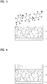
- FIG. 2 is a schematic diagram showing a precursor having a methyl group as an end group and FIGS. 3 and FIG. 4 are sectional schematic views illustrating an example of a method of doping graphene using substrate surface modification.
- a precursor polymer layer 2 is formed on the substrate 1 using the precursor having a methyl group (CH 3 ) shown in FIG. 2 .
- the polymer layer 2 may be formed using plasma enhanced chemical vapor deposition (PECVD).
- PECVD plasma enhanced chemical vapor deposition
- a polymer such as cyclohexane has a ring shape, but the ring is opened by plasma treatment such as plasma enhanced chemical vapor deposition (PECVD) to produce a radical molecule. Accordingly, the methyl group may be exposed to an end.
- PECVD plasma enhanced chemical vapor deposition
- the polymer layer 20 having a methyl group exposed to the end enables surface enhancement (modification) of the substrate 1.
- Such graphene 3 may be formed on a catalytic metal (not shown) and transferred to the substrate 1 provided with a polymer layer 2.
- a catalytic metal may be a metal such as Ni, Co, Fe, Pt, Au, Al, Cr, Cu, Mg, Mn, Mo, Rh, Si, Ta, Ti, W, U, V, Zr or the like, and may be a single layer of any one thereof or an alloy of at least two thereof.
- a method of forming graphene 3 includes chemical vapor deposition such as thermal chemical vapor deposition (CVD), inductively coupled plasma chemical vapor deposition (ICP-CVD), plasma enhanced chemical vapor deposition (PE-CVD), microwave CVD or the like.
- CVD thermal chemical vapor deposition
- ICP-CVD inductively coupled plasma chemical vapor deposition
- PE-CVD plasma enhanced chemical vapor deposition
- microwave CVD microwave CVD or the like.
- various methods such as rapid thermal annealing (RTA), atomic layer deposition (ALD) and physical vapor deposition (PVD) may be used.
- RTA rapid thermal annealing
- ALD atomic layer deposition
- PVD physical vapor deposition
- chemical vapor deposition is a method which grows graphene 3 by placing a catalytic metal in a chamber (not shown), feeding a carbon source thereto and providing suitable growth conditions.
- the carbon source can be supplied in a gas form such as methane (CH 4 ) or acetylene (C 2 H 2 ), or a solid form such as a powder or a polymer, or a liquid form such as bubbling alcohol.
- a gas form such as methane (CH 4 ) or acetylene (C 2 H 2 )
- a solid form such as a powder or a polymer
- a liquid form such as bubbling alcohol.
- carbon sources such as ethane, ethylene, ethanol, acetylene, propane, butane, butadiene, pentane, pentene, cyclopentadiene, hexane, cyclohexane, benzene and toluene may be used.
- graphene 3 can be directly formed on the substrate 10, instead of transferring the graphene 3 onto the substrate 1.
- the substrate 1 may include a polymer which includes at least one of polyethylene terephthalate (PET), triacetyl cellulose (TAC), and polycarbonate (PC).
- PET polyethylene terephthalate
- TAC triacetyl cellulose
- PC polycarbonate
- the substrate 10 may be formed using any one of PEC, TAC and PC.
- the graphene 3 may be disposed on the substrate 1 provided with the polymer layer 2.
- the substrate 1 may be a flexible substrate and the graphene 3 disposed on the flexile substrate may be used as an electrode of a flexible device.
- the graphene 3 when graphene 3 is disposed on the surface-modified substrate 1, the graphene 3 is doped by a methyl group, thus improving electrical properties.
- this doping effect may be n-type doping or p-type doping.
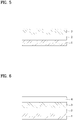
- FIGS. 5 to 7 are schematic sectional views illustrating examples of a graphene structure using substrate surface modification.
- graphene 3 is disposed on a substrate 1 which is surface-modified through a polymer layer 2 having a methyl group at an end thereof, to produce a graphene structure with improved electrical properties, that is, with doping effects.
- an additional doping layer 4 may be further included on the graphene structure having a structure shown in FIG. 5 .
- the graphene 3 disposed on the surface-modified substrate 1 can improve electrical properties through an additional doping process.
- the graphene 3 may exhibit n-type doping or p-type doping properties.
- Such a doping process can offset a decrease in conductivity by grain defects (defects at grain boundaries of metals) of graphene formed on a catalytic metal.
- the material of the graphene 3 is replaced with a dopant material contained in the doping layer 4, thus generating carriers. Accordingly, carrier density may be increased.
- the dopant for doping may include an organic dopant, an inorganic dopant or a combination thereof.
- a gas or solution of nitric acid and a material containing the same may be used.
- vapor phase doping using gas may be more advantageous.
- examples of this dopant include one or more of NO 2 BF 4 , NOBF 4 , NO 2 SbF 6 , HCl, H 2 PO 4 , CH 3 COOH, H 2 SO 4 , HNO 3 , PVDF, Nafion, AuCl 3 , SOCl 2 , Br 2 , CH 3 NO 2 , dichlorodicyanoquinone, oxone, dimyristoyl phosphatidylinositol, and trifluoromethanesulfonimide.
- the surface modification of the substrate 1 may be carried on both sides of the substrate 1. That is, a precursor polymer layer 2 is formed on both surfaces of the substrate 1 and graphene 3 is disposed on the polymer layer 2.
- the graphene 3 disposed on the substrate 1 surface-modified by the polymer layer 2 can exhibit greatly improved electrical properties, as described above.
- FIG. 8 is a graph showing current properties of graphene related to doping properties.
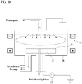
- FIG. 9 is a schematic view showing a PECVD procedure for conducting substrate surface modification
- FIGS. 10 and 11 are schematic diagrams illustrating a principle of polymerization using plasma by PECVD.
- the surface modification of the substrate 1 can be carried out by PECVD.
- a PECVD apparatus includes a chamber 100, and a magnetic coil 12 and an RF power supply 13 to generate plasma disposed in the chamber 100, wherein plasma is generated on a chuck 11 on which the substrate 1 is loaded.
- Backside cooling helium is supplied to a lower part of the chamber 100 to reduce the temperature of the substrate.
- process gases are supplied from an upper part and gases after reaction (by-products) are discharged through a pump (not shown) from a lower part.
- process gases are adsorbed on the surface of the substrate 1 cooled by the backside cooling helium and process gases activated by plasma react with process gases inactivated thereby to produce a polymer layer.
- deposition on the substrate 1 is considered to be adsorption of process gases due to orientation of plasma and low temperature of the surface of the substrate 1.
- M i refers to a polymer that is produced from i M molecules.
- the subscript "i" means the number (for example, k, j) of molecules that a polymer has.
- dot means a radical form.
- One dot means a single radical and two dots means two radicals.
- a radical can produce a bond by reaction with other molecules or radicals due to high reactivity of the radical.
- a polymer layer 2 can be formed by plasma.
- the ring of cyclohexane is opened by plasma treatment under a hydrogen atmosphere in a similar manner to the principle described in FIG. 10 , thus forming a radical molecule.
- the formed radical molecules having various structures undergo an increase in molecular weight as reaction occurs, like the manner described with reference to FIG. 10 .
- a precursor polymer layer 2 having a methyl group as an end group is uniformly formed on the substrate 1, and the polymer layer 2 can greatly improve properties of the substrate 1.
- FIG. 8 shows properties of graphene when using a polymer layer 2 having a chain precursor such as a methyl group. Doping effects are known to be maximized when a minimum of a current curve reaches around 0V.
- the functional group can be changed according to purpose and other properties of graphene can be improved depending on the functional group used.
- the graphene can be deposited on a flexible insulation material which replaces conventionally used silicon oxide inapplicable to flexible devices and is thus advantageously applicable to flexible devices.
- a graphene structure having high permeability can be manufactured and is thus applicable to optical devices, displays and the like.
- FIG. 12 is a flowchart illustrating an example of a method of manufacturing a graphene composite electrode.
- the method of manufacturing the graphene composite electrode includes forming graphene on a catalytic metal (S10), forming a transparent conductive layer on the graphene using a transparent conductive oxide (S20), crystallizing the transparent conductive oxide by heat treatment (S30) and transferring a composite electrode including the graphene and the transparent conductive oxide to a final substrate (S40).
- S10 catalytic metal
- S20 transparent conductive oxide
- S30 crystallizing the transparent conductive oxide by heat treatment
- S40 final substrate
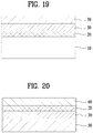
- FIGS. 13 to 20 are schematic sectional views illustrating respective steps of manufacturing a graphene composite electrode.
- graphene 20 is formed on a catalytic metal 10 (S20).
- the catalytic metal 10 may be a metal such as Ni, Co, Fe, Pt, Au, Al, Cr, Cu, Mg, Mn, Mo, Rh, Si, Ta, Ti, W, U, V, or Zr, and may be a single layer of any one thereof or an alloy of at least two thereof.
- the method of producing graphene 20 includes chemical vapor deposition such as thermal chemical vapor deposition (CVD), inductively coupled plasma chemical vapor deposition (ICP-CVD), plasma enhanced chemical vapor deposition (PECVD), and Microwave CVD.
- CVD thermal chemical vapor deposition
- ICP-CVD inductively coupled plasma chemical vapor deposition
- PECVD plasma enhanced chemical vapor deposition
- Microwave CVD various methods such as rapid thermal annealing (RTA), atomic layer deposition (ALD), and physical vapor deposition (PVD) may be used.
- RTA rapid thermal annealing
- ALD atomic layer deposition
- PVD physical vapor deposition
- chemical vapor deposition is a method which grows graphene 3 by placing a catalytic metal 10 in a chamber (not shown), feeding a carbon source thereto and providing suitable growth conditions.
- the carbon source can be supplied in a gas form such as methane (CH 4 ) or acetylene (C 2 H 2 ), or a solid form such as a powder or a polymer, or a liquid form such as bubbling alcohol.
- a gas form such as methane (CH 4 ) or acetylene (C 2 H 2 )
- a solid form such as a powder or a polymer
- a liquid form such as bubbling alcohol.
- carbon sources such as ethane, ethylene, ethanol, acetylene, propane, butane, butadiene, pentane, pentene, cyclopentadiene, hexane, cyclohexane, benzene and toluene may be used.
- the graphene 20 can be formed on only an upper surface of the catalytic metal 10.
- the graphene 20 can be formed on both surfaces of the catalytic metal 10.
- Copper as the catalytic metal 10 can be advantageous in forming mono-layer graphene to low solid solution degree.
- the graphene 20 may be directly formed on the catalytic metal 10.
- the catalytic metal 10 may be supplied in a sheet form, but can be continuously supplied using a roller, or a copper foil with a thickness of about 10 ⁇ m to 10 mm can be used as the catalytic metal 10. That is, using a roll-to-roll process, the graphene 20 can be formed on the catalytic metal 10.
- the graphene 20 obtained by the aforementioned process is formed at both surfaces as described above, the graphene 20 formed on one surface of the catalytic metal 10 may be removed.
- the graphene 20 can be formed on one surface of the catalytic metal 10.
- the conductivity of the graphene 20 can be improved. That is, grain defects resulting from the catalytic metal 10 (defects caused by the grain boundary or the like of the metal) may lead to deterioration in conductivity of the graphene 20.
- the material of the graphene 20 is replaced with the dopant material, which may generate carriers. Accordingly, carrier density may be increased.
- the dopant for doping may include an organic dopant, an inorganic dopant or a combination thereof.
- a gas or solution of nitric acid and a material containing the same may be used.
- vapor phase doping using gas may be more advantageous.
- examples of this dopant include one or more of NO 2 BF 4 , NOBF 4 , NO 2 SbF 6 , HCl, H 2 PO 4 , CH 3 COOH, H 2 SO 4 , HNO 3 , PVDF, Nafion, AuCl 3 , SOCl 2 , Br 2 , CH 3 NO 2 , dichlorodicyanoquinone, oxone, dimyristoyl phosphatidylinositol, and trifluoromethanesulfonimide.
- FIG. 14 shows a transparent conductive layer 31 formed on the graphene 20. As such, forming a transparent conductive layer on the graphene 20 using a transparent conductive oxide (S20) is conducted.
- S20 transparent conductive oxide
- the transparent conductive oxide may include at least one of indium tin oxide (ITO), indium zinc oxide (IZO), zinc oxide (ZnO), gallium doped zinc oxide (GZO) and aluminum doped zinc oxide (AZO).
- ITO indium tin oxide
- IZO indium zinc oxide
- ZnO zinc oxide
- GZO gallium doped zinc oxide
- AZO aluminum doped zinc oxide
- ITO is a material produced by conducting solid solution of SnO 2 in In 2 O 3 , which is an oxide having low electrical resistance and being stable at room temperature because it exhibits excellent transmittance in the visible light region, while exhibiting high reflectivity in an infrared light region.
- the step of crystallizing the transparent conductive oxide by heat treatment (S30) may be carried out at a temperature of 150°C to 400°C.
- This crystallization S30 can improve crystallinity of the transparent conductive layer 31 and reduce resistance.
- the crystallized transparent conductive layer 30 may be disposed on the graphene 20.
- Formation of the transparent conductive layer 31 (S20) and crystallization (S30) can be carried out using a sputtering device shown in FIG. 21 .
- FIG. 21 is a schematic view illustrating a process of forming a transparent conductive layer according to the present invention.
- the vacuum level of the chamber 100 is formed to 10 mTorr using a first vacuum pump (rotary pump; 110) and secondarily the vacuum level is formed to 3 ⁇ 10 -6 mTorr using a second vacuum pump (diffusion pump; 120).
- An RF power supply 150 has a power of 300W or higher and this may be adjusted upwardly or downwardly.
- the frequency applied is typically about 14 MHz, which may be adjusted upwardly or downwardly.
- Ar injection may be conducted to produce plasma and a small amount of oxygen may be injected together with the Ar to perform crystallization (S30).
- ITO 30 may be formed on the graphene 20 formed on the catalytic metal 10, and the graphene 20 is omitted as shown in FIG. 21 .
- the target 130 evaporates and ITO is formed as a transparent conductive layer 30 on the graphene 20.
- a permanent magnet 140 may be disposed under the target 130.
- the crystallized transparent conductive layer 30 is an ITO layer
- the transparent conductive layer 30 formed on the graphene 20 can produce a transparent composite electrode. That is, through the organic/inorganic hybrid of the graphene 20 and the ITO layer 30, a transparent composite electrode having low resistance can be formed.
- Such a composite electrode is applicable to a sputtering method which is currently industrially available. This can cause a 1/5 decrease in amount of ITO used. This is because the composite electrode satisfies all of conditions for the transparent electrode although it is formed at a small thickness.
- the ITO layer 30 can function as a protection film of the graphene 20.
- the effect of doping can be maintained for a longer time.
- the transfer (S40) may be broadly carried out by two methods.
- a temporary support layer is used.
- a support layer is disposed on an ITO layer 30.
- the support layer 40 may be adhered to the ITO layer 30 or directly formed thereon.
- the support layer 40 adhered to the ITO layer 30 may be a transfer film.
- the transfer film includes an adhesive layer and can be easily removed from the ITO layer 30 because it loses adhesion upon subsequent application of heat or light.
- the adhesive layer may be a reworkable adhesive agent. That is, the adhesive layer can be easily detached during or after a process, and does not leave resides behind even after detachment.
- the final substrate 50 may be adhered to the surface from which the catalytic metal 10 is removed. In some cases, the final substrate 50 may be directly formed on the surface from which the catalytic metal 10 is removed.
- the final substrate 50 may mean a layer which can be applied to an electronic device together with the graphene 20.
- the final substrate 50 may be a transparent or non-transparent substrate which can be directly used for various display devices and may be a substrate directly used for devices such as touch panels.
- the final substrate 50 may be a polymer material such as polyethylene terephthalate (PET), triacetyl cellulose (TAC), and polycarbonate (PC), or a semiconductor wafer such as silicon (Si). Furthermore, any member may be used without limitation so long as it is a transparent or non-transparent film.
- PET polyethylene terephthalate
- TAC triacetyl cellulose
- PC polycarbonate
- Si silicon
- any member may be used without limitation so long as it is a transparent or non-transparent film.
- the method may include removing the support layer 40.
- the composite electrode including the graphene 20 and the ITO layer 30 is disposed on the final substrate 50, as shown in FIG. 18 .
- the final substrate 50 may be directly adhered to or formed on the ITO layer 30 for transfer.
- the catalytic metal 10 may be removed.
- the composite electrode including the graphene 20 and the ITO layer 30 can be disposed on the final substrate 50.
- the ITO layer 30 is disposed directly on the final substrate 50.
- a flexible transparent electrode can be produced using the composite electrode transferred to the final substrate 50. That is, the composite electrode imparts both conductivity and flexibility, thus removing limitations of flexible displays which could not be overcome only with an ITO layer.
- the present process is applicable to an ITO roll-to-roll process, and can be used in combination with a roll-to-roll-based graphene synthesis process.
- the transparent composite electrode can be produced and the composite electrode including graphene 20 includes an organic material (graphene) and, in particular, thus exhibits excellent adhesion to an organic EL display.
- the method may further include forming an organic EL layer 60 on the graphene 20.
- the composite electrode produced according to the present invention can be used as a transparent electrode, in particular, a flexible electrode, of an organic EL display.
- the subject applied is not limited to the organic EL display.
- the composite electrode including the graphene 20 and the ITO layer 30 can be heat-treated at a temperature of 150°C to 400°C, thus greatly improving conductivity.
- heat-treatment at a temperature of 150°C or higher cannot be conducted. Accordingly, the transparent electrode produced according to the present invention can greatly improve conductivity, as compared to the conventional case.
- the thickness of the electrode can be reduced to half or less under the same conductivity, which means that the material for the electrode used is reduced.
- the surfaces of various substrates can be modified using a polymer layer including an organic precursor rapidly and at low cost.
- the graphene can be deposited on a flexible insulation material which replaces conventionally used silicon oxide inapplicable to flexible devices and is thus advantageously applicable to flexible devices.
- graphene structures having high permeability can be manufactured and are thus applicable to optical devices, displays and the like.
- Graphene disposed on a surface-modified substrate can exhibit improved electrical properties.
- the transparent conductive layer formed on the graphene can produce a transparent composite electrode. That is, a transparent composite electrode having low resistance can be formed through organic/inorganic hybrid of graphene and an ITO layer.
Landscapes
- Chemical & Material Sciences (AREA)
- Engineering & Computer Science (AREA)
- Materials Engineering (AREA)
- General Chemical & Material Sciences (AREA)
- Chemical Kinetics & Catalysis (AREA)
- Mechanical Engineering (AREA)
- Metallurgy (AREA)
- Organic Chemistry (AREA)
- Inorganic Chemistry (AREA)
- Manufacturing & Machinery (AREA)
- Plasma & Fusion (AREA)
- Physics & Mathematics (AREA)
- Manufacturing Of Electric Cables (AREA)
- Non-Insulated Conductors (AREA)
- Carbon And Carbon Compounds (AREA)
Abstract
Description
- The present invention relates to graphene, and particularly to a method of doping graphene using substrate surface modification, a method of manufacturing a graphene composite electrode using graphene and an inorganic material, and a graphene structure including the same.
- Fullerene, carbon nanotubes, graphene, graphite and the like are materials composed of carbon atoms. Thereamong, graphene has a structure composed of a single atomic layer of carbon atoms disposed in the form of a two-dimensional plane.
- In particular, graphene exhibits extremely stable excellent electrical, mechanical and chemical properties as well as superior conductivity, which transfers electrons much faster than silicon and conducts much greater electricity than copper. This was demonstrated by experimentation since a method of isolating graphene from graphite was found in 2004 and a great deal of research has been conducted to date.
- Such graphene draws a great deal of attention as a basic material for electrical circuits because it can be manufactured in a large area and exhibits electrical, mechanical and chemical stability as well as excellent conductivity.
- In addition, generally, electrical properties of graphene change depending on grain orientation of the graphene of a predetermined thickness and thus the graphene exhibits electrical properties in a direction selected by a user and, as a result, a device can be easily designed. Accordingly, graphene can be effectively used for carbon-based electronic or electromagnetic devices and the like.
- In general, application products such as display devices require a transparent electrode and extremely thick transparent conductive oxide films are used in order to maintain requirements for such a transparent electrode.
- However, such thick transparent electrodes may be inapplicable to deposition on plastic substrates to manufacture flexible devices and displays and may be unsuitable in terms of transparency and low surface roughness. Thus, there is a need for an alternative to this.
- Meanwhile, recently, silicon oxide dielectrics are applied to analyze device properties of graphene. In a conventional case, since p-type doping is obtained by doping the substrate, an undoped form obtained by additional heat treatment or self-assembled monolayer coating is used.
- In addition, surface modification could not be generally realized because there were cases in which heat-treatment cannot be conducted or a self-assembled monolayer cannot be formed on substrates other than silicon oxide. Accordingly, there is a limitation in doping effects of graphene and an approach to solve this problem is thus needed.
- One object of the present invention devised to solve the problem lies in a method of doping graphene and a graphene structure including the same.
- In addition, another object of the present invention devised to solve the problem lies in a method of doping graphene using substrate surface modification and a graphene structure including the same.
- Meanwhile, another object of the present invention devised to solve the problem lies in a method of manufacturing a graphene composite electrode using graphene and a transparent conductive layer.
- In addition, another object of the present invention devised to solve the problem lies in a method of manufacturing a graphene composite electrode which can reduce an electrode thickness and can be applied to flexible devices and displays.
- The object of the present invention can be achieved by providing a method of doping graphene using substrate surface modification including forming a precursor polymer layer for doping on a substrate and disposing graphene on the substrate provided with the precursor polymer layer.
- Here, the precursor polymer layer may include a precursor having a methyl group.
- In this case, the precursor polymer layer may include the precursor having the methyl group as an end group.
- In addition, the precursor having a methyl group may be a cyclohexane precursor.
- In this case, the cyclohexane precursor may include at least one of cyclohexane, methyl cyclohexane and ethyl cyclohexane.
- Here, the substrate may be a polymer substrate.
- In this case, the polymer substrate may include at least one of polyethylene terephthalate (PET), triacetyl cellulose (TAC), and polycarbonate (PC).
- Here, the formation of the precursor may be carried out using plasma enhanced chemical vapor deposition.
- Here, the method may further include doping the graphene.
- In another aspect of the present invention, provided herein is a graphene structure including a substrate, a precursor layer having a methyl group disposed on the substrate, and graphene disposed on the precursor layer.
- Here, the precursor having a methyl group may include at least one of cyclohexane, methyl cyclohexane and ethyl cyclohexane.
- Here, the substrate may include at least one of polyethylene terephthalate (PET), triacetyl cellulose (TAC), and polycarbonate (PC).
- In another aspect of the present invention, provided herein is a method of manufacturing a graphene composite electrode including forming graphene on a catalytic metal, forming a transparent conductive oxide on the graphene, crystallizing the transparent conductive oxide by applying heat of 150°C thereto, and transferring a composite electrode including the graphene and the transparent conductive oxide to a final substrate.
- Here, the method may further include doping the graphene after forming the graphene.
- Here, the crystallization may be carried out at a temperature of 150°C to 400°C.
- Here, the transparent conductive oxide may include at least one of ITO, IZO, ZnO, GZO and AZO.
- Here, the transfer may include disposing a support layer on the transparent conductive oxide, removing the catalytic metal, adhering the composite electrode to the final substrate, and removing the support layer.
- In addition, the transfer may include forming the final substrate on the transparent conductive oxide, and removing the catalytic metal.
- Here, the final substrate may be a polymer substrate.
- Here, the method may further include forming an organic EL layer on the graphene.
- The present invention has the following effects.
- The graphene disposed on the surface-modified substrate can improve electrical properties. In addition, graphene can exhibit a feature of n-type doping or p-type doping.
- Such a doping process can offset a decrease in conductivity caused by grain defects (defects at grain boundaries of metals) of graphene formed on a catalytic metal.
- In addition, in cases where additional doping is conducted through surface modification of the substrate using the polymer layer, it is possible to maximize the effects of doping.
- Meanwhile, the transparent conductive layer formed on the graphene can produce a transparent composite electrode. That is, through the organic/inorganic hybrid of the graphene and the ITO layer, a transparent composite electrode having low resistance can be formed.
- Such a composite electrode is applicable to a sputtering method which is currently industrially available. This can cause a 1/5 decrease in amount of ITO used. This is because the composite electrode satisfies all of conditions for the transparent electrode although it is formed to a small thickness.
- In addition, the ITO layer can function as a protection film of graphene. When the graphene is doped, the effect of doping can be maintained for a longer time.
- Meanwhile, through a composite electrode of graphene as a two-dimensional material and the ITO layer, it is possible to manufacture a flexible transparent electrode. That is, the composite electrode imparts both conductivity and flexibility, thus removing limitations of flexible displays which could not be overcome only with an ITO layer.
-
-
FIG. 1 is a flowchart illustrating an example of a method of doping graphene using substrate surface modification; -
FIG. 2 is a schematic diagram showing a precursor having a methyl group as an end group; -
FIGS. 3 and FIG. 4 are sectional schematic views illustrating an example of a method of doping graphene using substrate surface modification; -
FIGS. 5 to 7 are schematic sectional views illustrating examples of a graphene structure using substrate surface modification; -
FIG. 8 is a graph showing current properties of graphene related to doping properties; -
FIG. 9 is a schematic view showing PECVD for conducting substrate surface modification; -
FIGS. 10 and 11 are schematic diagrams illustrating a principle of polymerization using plasma; -
FIG. 12 is a flowchart illustrating an example of a method of manufacturing a graphene composite electrode; -
FIGS. 13 to 20 are schematic sectional views illustrating respective steps of manufacturing a graphene composite electrode; and -
FIG. 21 is a schematic view illustrating a process of forming a transparent conductive layer. - Reference will now be made in detail to the preferred embodiments of the present invention, examples of which are illustrated in the accompanying drawings.
- However, the present invention allows various modifications and variations and specific embodiments thereof are exemplified with reference to the drawings and will be described in detail. The present invention should not be construed as limited to the embodiments set forth herein and includes modifications, equivalents and substitutions compliant with the spirit or scope of the present invention defined by the appended claims.
- It will be understood that when an element such as a layer, area or substrate is referred to as being "on" another element, it may be directly on the element, or one or more intervening elements may also be present therebetween.
- In addition, it will be understood that although terms such as "first" and "second" may be used herein to describe elements, components, areas, layers and/or regions, the elements, components, areas, layers and/or regions should not be limited by these terms.
-
FIG. 1 is a flowchart illustrating an example of a method of doping graphene using substrate surface modification. - As shown in
FIG. 1 , the method may include forming a precursor polymer layer for doping on a substrate (S1) and disposing graphene on the substrate provided with the precursor polymer layer (S2). - Here, the precursor polymer layer may include a precursor having a methyl group (CH3).
- In this case, the precursor polymer layer may include a precursor having a methyl group as an end group. The precursor having a methyl group as an end group can improve conductivity of graphene by interaction between the methyl group of the precursor and the graphene or can provide conditions for doping graphene under optimal conditions. This will be described in detail later.
- The precursor having a methyl group may be a cyclohexane precursor. That is, the precursor having a methyl group may include at least one of cyclohexane, methyl cyclohexane and ethyl cyclohexane.
- The following Table 1 shows the structure of this cyclohexane precursor.

- Here, the substrate may be a polymer substrate.
- The polymer substrate may include at least one of polyethylene terephthalate (PET), triacetyl cellulose (TAC) and polycarbonate (PC).
- Hereinafter, respective steps will be described with reference to
FIG. 1 and the corresponding drawings. -
FIG. 2 is a schematic diagram showing a precursor having a methyl group as an end group andFIGS. 3 and FIG. 4 are sectional schematic views illustrating an example of a method of doping graphene using substrate surface modification. - As shown in
FIG. 3 , aprecursor polymer layer 2 is formed on thesubstrate 1 using the precursor having a methyl group (CH3) shown inFIG. 2 . - Here, the
polymer layer 2 may be formed using plasma enhanced chemical vapor deposition (PECVD). - A polymer such as cyclohexane has a ring shape, but the ring is opened by plasma treatment such as plasma enhanced chemical vapor deposition (PECVD) to produce a radical molecule. Accordingly, the methyl group may be exposed to an end.
- As such, the
polymer layer 20 having a methyl group exposed to the end enables surface enhancement (modification) of thesubstrate 1. -
Such graphene 3 may be formed on a catalytic metal (not shown) and transferred to thesubstrate 1 provided with apolymer layer 2. - A catalytic metal may be a metal such as Ni, Co, Fe, Pt, Au, Al, Cr, Cu, Mg, Mn, Mo, Rh, Si, Ta, Ti, W, U, V, Zr or the like, and may be a single layer of any one thereof or an alloy of at least two thereof.
- A method of forming
graphene 3 includes chemical vapor deposition such as thermal chemical vapor deposition (CVD), inductively coupled plasma chemical vapor deposition (ICP-CVD), plasma enhanced chemical vapor deposition (PE-CVD), microwave CVD or the like. In addition, various methods such as rapid thermal annealing (RTA), atomic layer deposition (ALD) and physical vapor deposition (PVD) may be used. - For example, chemical vapor deposition is a method which grows
graphene 3 by placing a catalytic metal in a chamber (not shown), feeding a carbon source thereto and providing suitable growth conditions. - For example, the carbon source can be supplied in a gas form such as methane (CH4) or acetylene (C2H2), or a solid form such as a powder or a polymer, or a liquid form such as bubbling alcohol.
- In addition, a variety of carbon sources such as ethane, ethylene, ethanol, acetylene, propane, butane, butadiene, pentane, pentene, cyclopentadiene, hexane, cyclohexane, benzene and toluene may be used.
- When a material which is not deformed at a high temperature, rather than a polymer substrate, is used as the
substrate 1,graphene 3 can be directly formed on thesubstrate 10, instead of transferring thegraphene 3 onto thesubstrate 1. - As described above, the
substrate 1 may include a polymer which includes at least one of polyethylene terephthalate (PET), triacetyl cellulose (TAC), and polycarbonate (PC). For example, thesubstrate 10 may be formed using any one of PEC, TAC and PC. - As shown in
FIG. 4 , thegraphene 3 may be disposed on thesubstrate 1 provided with thepolymer layer 2. - That is, the
substrate 1 may be a flexible substrate and thegraphene 3 disposed on the flexile substrate may be used as an electrode of a flexible device. - As such, when
graphene 3 is disposed on the surface-modifiedsubstrate 1, thegraphene 3 is doped by a methyl group, thus improving electrical properties. - In addition, this doping effect may be n-type doping or p-type doping.
-
FIGS. 5 to 7 are schematic sectional views illustrating examples of a graphene structure using substrate surface modification. - That is, as shown in
FIG. 5 ,graphene 3 is disposed on asubstrate 1 which is surface-modified through apolymer layer 2 having a methyl group at an end thereof, to produce a graphene structure with improved electrical properties, that is, with doping effects. - In addition, as shown in
FIG. 6 , anadditional doping layer 4 may be further included on the graphene structure having a structure shown inFIG. 5 . - That is, the
graphene 3 disposed on the surface-modifiedsubstrate 1 can improve electrical properties through an additional doping process. In addition, as described above, thegraphene 3 may exhibit n-type doping or p-type doping properties. - Such a doping process can offset a decrease in conductivity by grain defects (defects at grain boundaries of metals) of graphene formed on a catalytic metal.
- That is, the material of the
graphene 3 is replaced with a dopant material contained in thedoping layer 4, thus generating carriers. Accordingly, carrier density may be increased. - The dopant for doping may include an organic dopant, an inorganic dopant or a combination thereof. For example, a gas or solution of nitric acid and a material containing the same may be used. In particular, vapor phase doping using gas may be more advantageous.
- In addition, specifically, examples of this dopant include one or more of NO2BF4, NOBF4, NO2SbF6, HCl, H2PO4, CH3COOH, H2SO4, HNO3, PVDF, Nafion, AuCl3, SOCl2, Br2, CH3NO2, dichlorodicyanoquinone, oxone, dimyristoyl phosphatidylinositol, and trifluoromethanesulfonimide.
- Meanwhile, as shown in
FIG. 7 , the surface modification of thesubstrate 1 may be carried on both sides of thesubstrate 1. That is, aprecursor polymer layer 2 is formed on both surfaces of thesubstrate 1 andgraphene 3 is disposed on thepolymer layer 2. - As such, the
graphene 3 disposed on thesubstrate 1 surface-modified by thepolymer layer 2 can exhibit greatly improved electrical properties, as described above. -
FIG. 8 is a graph showing current properties of graphene related to doping properties. In addition,FIG. 9 is a schematic view showing a PECVD procedure for conducting substrate surface modification, andFIGS. 10 and 11 are schematic diagrams illustrating a principle of polymerization using plasma by PECVD. - Hereinafter, a procedure of substrate surface modification will be described with reference to
FIGS. 8 to 11 . - As described above, the surface modification of the
substrate 1 can be carried out by PECVD. - As shown in
FIG. 9 , a PECVD apparatus includes achamber 100, and amagnetic coil 12 and anRF power supply 13 to generate plasma disposed in thechamber 100, wherein plasma is generated on achuck 11 on which thesubstrate 1 is loaded. - Backside cooling helium is supplied to a lower part of the
chamber 100 to reduce the temperature of the substrate. - In
FIG. 9 , process gases are supplied from an upper part and gases after reaction (by-products) are discharged through a pump (not shown) from a lower part. - In accordance with this PECVD method, process gases are adsorbed on the surface of the
substrate 1 cooled by the backside cooling helium and process gases activated by plasma react with process gases inactivated thereby to produce a polymer layer. - Here, deposition on the
substrate 1 is considered to be adsorption of process gases due to orientation of plasma and low temperature of the surface of thesubstrate 1. - Hereinafter, a reaction principle of forming this polymer layer will be described.
- In
FIG. 10 , Mi refers to a polymer that is produced from i M molecules. Thus, the subscript "i" means the number (for example, k, j) of molecules that a polymer has. - In addition, dot means a radical form.
- One dot means a single radical and two dots means two radicals.
- A radical can produce a bond by reaction with other molecules or radicals due to high reactivity of the radical.
- Here, "+" means reaction between two materials. The product obtained by reaction between two materials is disposed in a direction of a head of an arrow and a bond occurs after reaction.
- In addition, "-" means formation of a bond between molecules.
- Through such a process, a
polymer layer 2 can be formed by plasma. - Referring to
FIG. 11 , in the case of cyclohexane having a ring shape, the ring of cyclohexane is opened by plasma treatment under a hydrogen atmosphere in a similar manner to the principle described inFIG. 10 , thus forming a radical molecule. - The formed radical molecules having various structures undergo an increase in molecular weight as reaction occurs, like the manner described with reference to
FIG. 10 . - Through such a process, a
precursor polymer layer 2 having a methyl group as an end group is uniformly formed on thesubstrate 1, and thepolymer layer 2 can greatly improve properties of thesubstrate 1. -
FIG. 8 shows properties of graphene when using apolymer layer 2 having a chain precursor such as a methyl group. Doping effects are known to be maximized when a minimum of a current curve reaches around 0V. - As shown in
FIG. 8 , a minimum of a current curve reaches around 0V. Whengraphene 3 is disposed on thepolymer layer 2, electrical properties of thegraphene 3 can be improved by bonding with thepolymer layer 2. - In addition, through surface modification of the
substrate 1 using thepolymer layer 2, in case where additional doping is conducted, it is possible to maximize the effects of doping. - In the present embodiment, an example of using the
polymer layer 2 for doping properties including conductivity enhancement has been described, but various properties can be improved depending on the type of the polymer. - For example, the functional group can be changed according to purpose and other properties of graphene can be improved depending on the functional group used.
- As a result, it is possible to modify the surface of various substrates promptly at a low cost by using a polymer layer including an organic precursor.
- The graphene can be deposited on a flexible insulation material which replaces conventionally used silicon oxide inapplicable to flexible devices and is thus advantageously applicable to flexible devices.
- In addition, a graphene structure having high permeability can be manufactured and is thus applicable to optical devices, displays and the like.
-
FIG. 12 is a flowchart illustrating an example of a method of manufacturing a graphene composite electrode. - As shown in
FIG. 12 , the method of manufacturing the graphene composite electrode includes forming graphene on a catalytic metal (S10), forming a transparent conductive layer on the graphene using a transparent conductive oxide (S20), crystallizing the transparent conductive oxide by heat treatment (S30) and transferring a composite electrode including the graphene and the transparent conductive oxide to a final substrate (S40). Hereinafter, respective steps will be described with reference toFIG. 12 and the corresponding drawings. -
FIGS. 13 to 20 are schematic sectional views illustrating respective steps of manufacturing a graphene composite electrode. - As shown in
FIG. 13 , in order to produce a composite electrode including graphene,graphene 20 is formed on a catalytic metal 10 (S20). - The
catalytic metal 10 may be a metal such as Ni, Co, Fe, Pt, Au, Al, Cr, Cu, Mg, Mn, Mo, Rh, Si, Ta, Ti, W, U, V, or Zr, and may be a single layer of any one thereof or an alloy of at least two thereof. - The method of producing
graphene 20 includes chemical vapor deposition such as thermal chemical vapor deposition (CVD), inductively coupled plasma chemical vapor deposition (ICP-CVD), plasma enhanced chemical vapor deposition (PECVD), and Microwave CVD. In addition, various methods such as rapid thermal annealing (RTA), atomic layer deposition (ALD), and physical vapor deposition (PVD) may be used. - For example, chemical vapor deposition is a method which grows
graphene 3 by placing acatalytic metal 10 in a chamber (not shown), feeding a carbon source thereto and providing suitable growth conditions. - For example, the carbon source can be supplied in a gas form such as methane (CH4) or acetylene (C2H2), or a solid form such as a powder or a polymer, or a liquid form such as bubbling alcohol.
- In addition, a variety of carbon sources such as ethane, ethylene, ethanol, acetylene, propane, butane, butadiene, pentane, pentene, cyclopentadiene, hexane, cyclohexane, benzene and toluene may be used.
- Hereinafter, an example in which copper (Cu) is used as the
catalytic metal 10 and methane (CH4) is used as the carbon source will be described. - When methane gas is supplied onto the
catalytic metal 10 under a hydrogen atmosphere while maintaining a suitable temperature, hydrogen reacts with methane to formgraphene 20 on thecatalytic metal 10. Formation of thegraphene 20 can be carried out at a temperature of about 300 to about 1,500°C. - At this time, when there is no space on a lower surface of the
catalytic metal 10, thegraphene 20 can be formed on only an upper surface of thecatalytic metal 10. On the other hand, when there is a space on the lower surface of thecatalytic metal 10, thegraphene 20 can be formed on both surfaces of thecatalytic metal 10. - Copper as the
catalytic metal 10 can be advantageous in forming mono-layer graphene to low solid solution degree. Thegraphene 20 may be directly formed on thecatalytic metal 10. - The
catalytic metal 10 may be supplied in a sheet form, but can be continuously supplied using a roller, or a copper foil with a thickness of about 10 µm to 10 mm can be used as thecatalytic metal 10. That is, using a roll-to-roll process, thegraphene 20 can be formed on thecatalytic metal 10. - When the
graphene 20 obtained by the aforementioned process is formed at both surfaces as described above, thegraphene 20 formed on one surface of thecatalytic metal 10 may be removed. - Through this process, as shown in
FIG. 13 , thegraphene 20 can be formed on one surface of thecatalytic metal 10. - Then, doping the graphene 20 (S 11) is conducted.
- Through this doping process (S11), the conductivity of the
graphene 20 can be improved. That is, grain defects resulting from the catalytic metal 10 (defects caused by the grain boundary or the like of the metal) may lead to deterioration in conductivity of thegraphene 20. In this regard, the material of thegraphene 20 is replaced with the dopant material, which may generate carriers. Accordingly, carrier density may be increased. - The dopant for doping may include an organic dopant, an inorganic dopant or a combination thereof. For example, a gas or solution of nitric acid and a material containing the same may be used. In particular, vapor phase doping using gas may be more advantageous.
- In addition, specifically, examples of this dopant include one or more of NO2BF4, NOBF4, NO2SbF6, HCl, H2PO4, CH3COOH, H2SO4, HNO3, PVDF, Nafion, AuCl3, SOCl2, Br2, CH3NO2, dichlorodicyanoquinone, oxone, dimyristoyl phosphatidylinositol, and trifluoromethanesulfonimide.
-
FIG. 14 shows a transparentconductive layer 31 formed on thegraphene 20. As such, forming a transparent conductive layer on thegraphene 20 using a transparent conductive oxide (S20) is conducted. - Here, the transparent conductive oxide (TCO) may include at least one of indium tin oxide (ITO), indium zinc oxide (IZO), zinc oxide (ZnO), gallium doped zinc oxide (GZO) and aluminum doped zinc oxide (AZO).
- Among them, ITO is a material produced by conducting solid solution of SnO2 in In2O3, which is an oxide having low electrical resistance and being stable at room temperature because it exhibits excellent transmittance in the visible light region, while exhibiting high reflectivity in an infrared light region.
- Then, crystallizing the transparent conductive oxide by heat treatment (S30) is conducted.
- The step of crystallizing the transparent conductive oxide by heat treatment (S30) may be carried out at a temperature of 150°C to 400°C.
- This crystallization S30 can improve crystallinity of the transparent
conductive layer 31 and reduce resistance. Thus, as shown inFIG. 15 , the crystallized transparentconductive layer 30 may be disposed on thegraphene 20. - Formation of the transparent conductive layer 31 (S20) and crystallization (S30) can be carried out using a sputtering device shown in
FIG. 21 . -
FIG. 21 is a schematic view illustrating a process of forming a transparent conductive layer according to the present invention. - First, primarily, the vacuum level of the
chamber 100 is formed to 10 mTorr using a first vacuum pump (rotary pump; 110) and secondarily the vacuum level is formed to 3×10⁻⁶ mTorr using a second vacuum pump (diffusion pump; 120). - An RF power supply 150 has a power of 300W or higher and this may be adjusted upwardly or downwardly. The frequency applied is typically about 14 MHz, which may be adjusted upwardly or downwardly.
- Ar injection may be conducted to produce plasma and a small amount of oxygen may be injected together with the Ar to perform crystallization (S30).
- Through this process,
ITO 30 may be formed on thegraphene 20 formed on thecatalytic metal 10, and thegraphene 20 is omitted as shown inFIG. 21 . - When plasma is produced at a side of a
target 130 upon application of power from the RF power supply 150, thetarget 130 evaporates and ITO is formed as a transparentconductive layer 30 on thegraphene 20. Apermanent magnet 140 may be disposed under thetarget 130. - Hereinafter, an example in which the crystallized transparent
conductive layer 30 is an ITO layer will be described. - The transparent
conductive layer 30 formed on thegraphene 20 can produce a transparent composite electrode. That is, through the organic/inorganic hybrid of thegraphene 20 and theITO layer 30, a transparent composite electrode having low resistance can be formed. - Such a composite electrode is applicable to a sputtering method which is currently industrially available. This can cause a 1/5 decrease in amount of ITO used. This is because the composite electrode satisfies all of conditions for the transparent electrode although it is formed at a small thickness.
- In addition, the
ITO layer 30 can function as a protection film of thegraphene 20. When thegraphene 20 is doped, the effect of doping can be maintained for a longer time. - Then, transferring a composite electrode including the graphene and the transparent conductive oxide to a final substrate (S40) is conducted.
- The transfer (S40) may be broadly carried out by two methods.
- First, a temporary support layer is used.
- For this purpose, as shown in
FIG. 16 , a support layer is disposed on anITO layer 30. Thesupport layer 40 may be adhered to theITO layer 30 or directly formed thereon. Thesupport layer 40 adhered to theITO layer 30 may be a transfer film. The transfer film includes an adhesive layer and can be easily removed from theITO layer 30 because it loses adhesion upon subsequent application of heat or light. - In addition, the adhesive layer may be a reworkable adhesive agent. That is, the adhesive layer can be easily detached during or after a process, and does not leave resides behind even after detachment.
- Next, as shown in
FIG. 17 , removal of thecatalytic metal 10 is conducted. - Then, the
final substrate 50 may be adhered to the surface from which thecatalytic metal 10 is removed. In some cases, thefinal substrate 50 may be directly formed on the surface from which thecatalytic metal 10 is removed. - The
final substrate 50 may mean a layer which can be applied to an electronic device together with thegraphene 20. - That is, the
final substrate 50 may be a transparent or non-transparent substrate which can be directly used for various display devices and may be a substrate directly used for devices such as touch panels. - The
final substrate 50 may be a polymer material such as polyethylene terephthalate (PET), triacetyl cellulose (TAC), and polycarbonate (PC), or a semiconductor wafer such as silicon (Si). Furthermore, any member may be used without limitation so long as it is a transparent or non-transparent film. - Then, the method may include removing the
support layer 40. When thesupport layer 40 is removed, the composite electrode including thegraphene 20 and theITO layer 30 is disposed on thefinal substrate 50, as shown inFIG. 18 . - Meanwhile, without using a support layer, the
final substrate 50 may be directly adhered to or formed on theITO layer 30 for transfer. - Then, the
catalytic metal 10 may be removed. - Through this transfer method, the composite electrode including the
graphene 20 and theITO layer 30 can be disposed on thefinal substrate 50. However, as shown inFIG. 20 , theITO layer 30 is disposed directly on thefinal substrate 50. - As such, a flexible transparent electrode can be produced using the composite electrode transferred to the
final substrate 50. That is, the composite electrode imparts both conductivity and flexibility, thus removing limitations of flexible displays which could not be overcome only with an ITO layer. - As described above, the present process is applicable to an ITO roll-to-roll process, and can be used in combination with a roll-to-roll-based graphene synthesis process.
- Through the hybrid of this two-dimensional material the
graphene 20 and theITO layer 30, the transparent composite electrode can be produced and the compositeelectrode including graphene 20 includes an organic material (graphene) and, in particular, thus exhibits excellent adhesion to an organic EL display. - Accordingly, as shown in
FIG. 20 , the method may further include forming anorganic EL layer 60 on thegraphene 20. As such, the composite electrode produced according to the present invention can be used as a transparent electrode, in particular, a flexible electrode, of an organic EL display. However, the subject applied is not limited to the organic EL display. - As described above, the composite electrode including the
graphene 20 and theITO layer 30 can be heat-treated at a temperature of 150°C to 400°C, thus greatly improving conductivity. In cases where only an ITO disposed on a conventional polymer substrate is used for a transparent electrode, heat-treatment at a temperature of 150°C or higher cannot be conducted. Accordingly, the transparent electrode produced according to the present invention can greatly improve conductivity, as compared to the conventional case. - In addition, as a result, the thickness of the electrode can be reduced to half or less under the same conductivity, which means that the material for the electrode used is reduced.
- Meanwhile, although embodiments according to the present invention disclosed in the specification and the drawings have been provided as specific examples for illustrative purposes, they should not be construed as limiting the scope of the present invention. It will be apparent to those skilled in the art that various modifications and variations can be made in the present invention without departing from the spirit or scope of the invention.
- The surfaces of various substrates can be modified using a polymer layer including an organic precursor rapidly and at low cost.
- The graphene can be deposited on a flexible insulation material which replaces conventionally used silicon oxide inapplicable to flexible devices and is thus advantageously applicable to flexible devices.
- In addition, graphene structures having high permeability can be manufactured and are thus applicable to optical devices, displays and the like.
- Graphene disposed on a surface-modified substrate can exhibit improved electrical properties.
- Meanwhile, the transparent conductive layer formed on the graphene can produce a transparent composite electrode. That is, a transparent composite electrode having low resistance can be formed through organic/inorganic hybrid of graphene and an ITO layer.
Claims (20)
- A method of doping graphene using substrate surface modification comprising:forming a precursor polymer layer for doping on a substrate; anddisposing graphene on the substrate provided with the precursor polymer layer.
- The method according to claim 1, wherein the precursor polymer layer comprises a precursor having a methyl group.
- The method according to claim 2, wherein the precursor polymer layer comprises the precursor having the methyl group as an end group.
- The method according to claim 2, wherein the precursor having a methyl group is a cyclohexane precursor.
- The method according to claim 4, wherein the cyclohexane precursor comprises at least one of cyclohexane, methyl cyclohexane and ethyl cyclohexane.
- The method according to claim 1, wherein the substrate is a polymer substrate.
- The method according to claim 6, wherein the polymer substrate comprises at least one of polyethylene terephthalate (PET), triacetyl cellulose (TAC), and polycarbonate (PC).
- The method according to claim 1, wherein the formation of the precursor is carried out using plasma enhanced chemical vapor deposition.
- The method according to claim 1, further comprising: doping the graphene.
- A graphene structure comprising:a substrate;a precursor layer having a methyl group disposed on the substrate; andgraphene disposed on the precursor layer.
- The graphene structure according to claim 10, wherein the precursor having a methyl group comprises at least one of cyclohexane, methyl cyclohexane and ethyl cyclohexane.
- The graphene structure according to claim 10, wherein the substrate comprises at least one of polyethylene terephthalate (PET), triacetyl cellulose (TAC), and polycarbonate (PC).
- A method of manufacturing a graphene composite electrode comprising:forming graphene on a catalytic metal;forming a transparent conductive oxide on the graphene;crystallizing the transparent conductive oxide by applying heat of 150°C thereto; andtransferring a composite electrode including the graphene and the transparent conductive oxide to a final substrate.
- The method according to claim 13, further comprising:doping the graphene after forming the graphene.
- The method according to claim 13, wherein the crystallization is carried out at a temperature of 150°C to 400°C.
- The method according to claim 13, wherein the transparent conductive oxide comprises at least one of ITO, IZO, ZnO, GZO and AZO.
- The method according to claim 13, wherein the transfer comprises:disposing a support layer on the transparent conductive oxide;removing the catalytic metal;adhering the composite electrode to the final substrate; andremoving the support layer.
- The method according to claim 13, wherein the transfer comprises:forming the final substrate on the transparent conductive oxide; andremoving the catalytic metal.
- The method according to claim 13, wherein the final substrate is a polymer substrate.
- The method according to claim 13, further comprising:forming an organic EL layer on the graphene.
Applications Claiming Priority (3)
| Application Number | Priority Date | Filing Date | Title |
|---|---|---|---|
| KR1020150052902A KR101706963B1 (en) | 2015-04-15 | 2015-04-15 | Method for manufacturing graphene hybrid electrode |
| KR1020150052901A KR101753590B1 (en) | 2015-04-15 | 2015-04-15 | Method for doping graphene using substrate of improved surface and graphine structure having the same |
| PCT/KR2016/003910 WO2016167583A1 (en) | 2015-04-15 | 2016-04-15 | Method for doping graphene, method for manufacturing graphene composite electrode, and graphene structure comprising same |
Publications (3)
| Publication Number | Publication Date |
|---|---|
| EP3284718A1 true EP3284718A1 (en) | 2018-02-21 |
| EP3284718A4 EP3284718A4 (en) | 2018-11-14 |
| EP3284718B1 EP3284718B1 (en) | 2020-06-10 |
Family
ID=57127268
Family Applications (1)
| Application Number | Title | Priority Date | Filing Date |
|---|---|---|---|
| EP16780306.3A Active EP3284718B1 (en) | 2015-04-15 | 2016-04-15 | Method for doping graphene, and graphene structure |
Country Status (4)
| Country | Link |
|---|---|
| US (1) | US10497893B2 (en) |
| EP (1) | EP3284718B1 (en) |
| CN (1) | CN107635918B (en) |
| WO (1) | WO2016167583A1 (en) |
Families Citing this family (9)
| Publication number | Priority date | Publication date | Assignee | Title |
|---|---|---|---|---|
| CN109421402B (en) * | 2017-08-29 | 2020-09-22 | 武汉大学 | A kind of laser engraving preparation method of highly conductive graphene thin film array |
| KR20210095644A (en) | 2018-11-30 | 2021-08-02 | 더 리서치 파운데이션 포 더 스테이트 유니버시티 오브 뉴욕 | Method for preparing n-doped graphene film |
| KR102887169B1 (en) * | 2019-12-03 | 2025-11-14 | 삼성전자주식회사 | method of forming graphene |
| CN110963484A (en) * | 2019-12-23 | 2020-04-07 | 中国科学院长春光学精密机械与物理研究所 | Large-area high-quality graphene lossless transfer method based on doping layer assistance |
| WO2022054150A1 (en) * | 2020-09-09 | 2022-03-17 | 株式会社 東芝 | Transparent electrode, method for manufacturing transparent electrode, and electronic device |
| US12312679B2 (en) * | 2020-12-22 | 2025-05-27 | Joz̃Stefan Institute | Method for producing N-doped carbon nanomesh |
| CN113092545B (en) * | 2021-04-13 | 2022-12-09 | 哈尔滨理工大学 | A preparation method of graphene MEMS gas sensor based on CuO/In2O3 modification |
| CN113410335B (en) * | 2021-06-17 | 2022-10-21 | 河北大学 | Preparation method of hole transport layer and crystalline silicon solar cell |
| KR20230086169A (en) | 2021-12-08 | 2023-06-15 | 삼성전자주식회사 | Electrode structure including metal and heat dissipation layer and semiconductor device including the same |
Family Cites Families (13)
| Publication number | Priority date | Publication date | Assignee | Title |
|---|---|---|---|---|
| JP4182673B2 (en) | 2002-04-10 | 2008-11-19 | セイコーエプソン株式会社 | Electro-optical device manufacturing method and electro-optical device manufacturing method |
| US6852474B2 (en) * | 2002-04-30 | 2005-02-08 | Brewer Science Inc. | Polymeric antireflective coatings deposited by plasma enhanced chemical vapor deposition |
| KR101603766B1 (en) | 2009-11-13 | 2016-03-15 | 삼성전자주식회사 | Graphene laminate and process for preparing the same |
| US8822042B2 (en) * | 2010-06-28 | 2014-09-02 | The University Of Southern California | Luminescent cyclometallated iridium(III) complexes having acetylide ligands |
| KR101680761B1 (en) | 2010-09-17 | 2016-11-30 | 삼성전자주식회사 | Graphene-polymer layered composite and process for preparing the same |
| CN102195006A (en) * | 2011-04-26 | 2011-09-21 | 福州大学 | Flexible electrode based on AZO/graphene/AZO structure and preparation method thereof |
| KR101295664B1 (en) * | 2011-06-24 | 2013-08-13 | 그래핀스퀘어 주식회사 | Stable graphene film and preparing method of the same |
| KR101166528B1 (en) | 2011-07-29 | 2012-07-19 | 주식회사 엘엠에스 | Graphene Laminates with Dopants and Manufacturing Method Thereof |
| KR101275636B1 (en) | 2011-08-30 | 2013-06-17 | 전자부품연구원 | Laminate with graphene comprising doped-polymer layer |
| KR101221581B1 (en) | 2011-10-20 | 2013-01-14 | 한국기계연구원 | Fabrication method of flexible transparent electrode substrate with graphene, and the flexible transparent electrode substrate substrate thereby |
| KR101437142B1 (en) | 2011-10-28 | 2014-09-02 | 제일모직주식회사 | Barrier film including graphene layer and flexible therof |
| CN103345963B (en) * | 2013-06-28 | 2015-07-15 | 重庆墨希科技有限公司 | Graphene composite transparent electrode and preparation method and application thereof |
| CN103963403A (en) * | 2014-04-25 | 2014-08-06 | 无锡格菲电子薄膜科技有限公司 | Composite of graphene and conducting polymer and preparation method of composite |
-
2016
- 2016-04-15 CN CN201680021660.5A patent/CN107635918B/en active Active
- 2016-04-15 WO PCT/KR2016/003910 patent/WO2016167583A1/en not_active Ceased
- 2016-04-15 US US15/563,087 patent/US10497893B2/en active Active
- 2016-04-15 EP EP16780306.3A patent/EP3284718B1/en active Active
Also Published As
| Publication number | Publication date |
|---|---|
| CN107635918A (en) | 2018-01-26 |
| EP3284718A4 (en) | 2018-11-14 |
| EP3284718B1 (en) | 2020-06-10 |
| CN107635918B (en) | 2021-03-09 |
| WO2016167583A1 (en) | 2016-10-20 |
| US10497893B2 (en) | 2019-12-03 |
| US20180083220A1 (en) | 2018-03-22 |
Similar Documents
| Publication | Publication Date | Title |
|---|---|---|
| EP3284718B1 (en) | Method for doping graphene, and graphene structure | |
| JP5705315B2 (en) | Low temperature manufacturing method of graphene and direct transfer method of graphene using the same | |
| US11124870B2 (en) | Transfer-free method for producing graphene thin film | |
| KR101806917B1 (en) | Method for manufacturing graphene | |
| KR102949672B1 (en) | Method for forming transition metal dichalcogenide film | |
| US8859044B2 (en) | Method of preparing graphene layer | |
| US10246795B2 (en) | Transfer-free method for forming graphene layer | |
| CN105152162B (en) | The batch large area preparation method of two-dimensional material film | |
| US20120261167A1 (en) | Transparent Electrodes, Electrode Devices, and Associated Methods | |
| WO2012134161A2 (en) | Graphene sheet, transparent electrode including graphene sheet, active layer, and display device, electronic device, photovoltaic device, battery, solar cell, and dye-sensitized solar cell employing transparent electrode | |
| CN104638071B (en) | A kind of nitride LED epitaxial slice structure of use compound substrate and preparation method thereof | |
| JP2012156202A (en) | Graphene/polymer laminate and application of the same | |
| Xiong et al. | Transparent electrodes based on ultrathin/ultra smooth Cu films produced through atomic layer deposition as new ITO-free organic light-emitting devices | |
| KR102017251B1 (en) | Method for Preparation of Graphene Thin Film without Transfer Process | |
| KR101802946B1 (en) | Process for formation of metal oxide film on graphene | |
| CN102576653B (en) | Semiconductor substrate, method for production of semiconductor layer, method for production of semiconductor substrate, semiconductor element, luminescent element, display panel, electronic element, solar battery element, and electronic device | |
| KR20170142361A (en) | Graphene complex electrode and manufacturing method thereof | |
| KR101706963B1 (en) | Method for manufacturing graphene hybrid electrode | |
| JP2010225384A (en) | Substrate with transparent electrode, and method for manufacturing the same | |
| KR101461977B1 (en) | Method for doping graphene layer | |
| KR101613558B1 (en) | Method for doping graphene layer | |
| KR20140062250A (en) | Method for manufacturing graphene and the graphene manufactured by the same | |
| JP5756834B2 (en) | Transfer film, method for producing the same, and method for producing transparent conductive laminate | |
| KR20120087844A (en) | Method for manufacturing graphene, transparent electrode, active layer comprising thereof, display, electronic device, optoelectronic device, battery, solar cell and dye-sensitized solar cell including the electrode or active layer | |
| CN106591798A (en) | Method for preparing graphene through non-adhesion inserting layer metal foil stacking |
Legal Events
| Date | Code | Title | Description |
|---|---|---|---|
| STAA | Information on the status of an ep patent application or granted ep patent |
Free format text: STATUS: THE INTERNATIONAL PUBLICATION HAS BEEN MADE |
|
| PUAI | Public reference made under article 153(3) epc to a published international application that has entered the european phase |
Free format text: ORIGINAL CODE: 0009012 |
|
| STAA | Information on the status of an ep patent application or granted ep patent |
Free format text: STATUS: REQUEST FOR EXAMINATION WAS MADE |
|
| 17P | Request for examination filed |
Effective date: 20171103 |
|
| AK | Designated contracting states |
Kind code of ref document: A1 Designated state(s): AL AT BE BG CH CY CZ DE DK EE ES FI FR GB GR HR HU IE IS IT LI LT LU LV MC MK MT NL NO PL PT RO RS SE SI SK SM TR |
|
| AX | Request for extension of the european patent |
Extension state: BA ME |
|
| DAV | Request for validation of the european patent (deleted) | ||
| DAX | Request for extension of the european patent (deleted) | ||
| A4 | Supplementary search report drawn up and despatched |
Effective date: 20181016 |
|
| RIC1 | Information provided on ipc code assigned before grant |
Ipc: C01B 32/20 20170101ALI20181010BHEP Ipc: H01L 29/16 20060101ALI20181010BHEP Ipc: C23C 16/26 20060101AFI20181010BHEP Ipc: H01L 21/283 20060101ALI20181010BHEP Ipc: H01B 1/04 20060101ALI20181010BHEP |
|
| RIC1 | Information provided on ipc code assigned before grant |
Ipc: C01B 32/20 20170101ALI20181010BHEP Ipc: H01L 29/16 20060101ALI20181010BHEP Ipc: H01B 1/04 20060101ALI20181010BHEP Ipc: H01L 21/283 20060101ALI20181010BHEP Ipc: C23C 16/26 20060101AFI20181010BHEP |
|
| REG | Reference to a national code |
Ref country code: DE Ref legal event code: R079 Ref document number: 602016037942 Country of ref document: DE Free format text: PREVIOUS MAIN CLASS: C01B0031040000 Ipc: C23C0016260000 |
|
| GRAP | Despatch of communication of intention to grant a patent |
Free format text: ORIGINAL CODE: EPIDOSNIGR1 |
|
| STAA | Information on the status of an ep patent application or granted ep patent |
Free format text: STATUS: GRANT OF PATENT IS INTENDED |
|
| RIC1 | Information provided on ipc code assigned before grant |
Ipc: C23C 16/26 20060101AFI20191121BHEP Ipc: H01L 29/16 20060101ALI20191121BHEP Ipc: H01L 21/283 20060101ALI20191121BHEP Ipc: C01B 32/20 20170101ALI20191121BHEP Ipc: H01B 1/04 20060101ALI20191121BHEP |
|
| RIC1 | Information provided on ipc code assigned before grant |
Ipc: H01L 21/283 20060101ALI20191129BHEP Ipc: C01B 32/194 20170101ALI20191129BHEP Ipc: C23C 16/26 20060101AFI20191129BHEP Ipc: H01L 29/16 20060101ALI20191129BHEP Ipc: H01B 1/04 20060101ALI20191129BHEP |
|
| INTG | Intention to grant announced |
Effective date: 20191218 |
|
| GRAS | Grant fee paid |
Free format text: ORIGINAL CODE: EPIDOSNIGR3 |
|
| GRAA | (expected) grant |
Free format text: ORIGINAL CODE: 0009210 |
|
| STAA | Information on the status of an ep patent application or granted ep patent |
Free format text: STATUS: THE PATENT HAS BEEN GRANTED |
|
| AK | Designated contracting states |
Kind code of ref document: B1 Designated state(s): AL AT BE BG CH CY CZ DE DK EE ES FI FR GB GR HR HU IE IS IT LI LT LU LV MC MK MT NL NO PL PT RO RS SE SI SK SM TR |
|
| REG | Reference to a national code |
Ref country code: GB Ref legal event code: FG4D |
|
| REG | Reference to a national code |
Ref country code: CH Ref legal event code: EP Ref country code: AT Ref legal event code: REF Ref document number: 1279255 Country of ref document: AT Kind code of ref document: T Effective date: 20200615 |
|
| REG | Reference to a national code |
Ref country code: DE Ref legal event code: R096 Ref document number: 602016037942 Country of ref document: DE |
|
| REG | Reference to a national code |
Ref country code: IE Ref legal event code: FG4D |
|
| REG | Reference to a national code |
Ref country code: LT Ref legal event code: MG4D |
|
| PG25 | Lapsed in a contracting state [announced via postgrant information from national office to epo] |
Ref country code: NO Free format text: LAPSE BECAUSE OF FAILURE TO SUBMIT A TRANSLATION OF THE DESCRIPTION OR TO PAY THE FEE WITHIN THE PRESCRIBED TIME-LIMIT Effective date: 20200910 Ref country code: FI Free format text: LAPSE BECAUSE OF FAILURE TO SUBMIT A TRANSLATION OF THE DESCRIPTION OR TO PAY THE FEE WITHIN THE PRESCRIBED TIME-LIMIT Effective date: 20200610 Ref country code: SE Free format text: LAPSE BECAUSE OF FAILURE TO SUBMIT A TRANSLATION OF THE DESCRIPTION OR TO PAY THE FEE WITHIN THE PRESCRIBED TIME-LIMIT Effective date: 20200610 Ref country code: LT Free format text: LAPSE BECAUSE OF FAILURE TO SUBMIT A TRANSLATION OF THE DESCRIPTION OR TO PAY THE FEE WITHIN THE PRESCRIBED TIME-LIMIT Effective date: 20200610 Ref country code: GR Free format text: LAPSE BECAUSE OF FAILURE TO SUBMIT A TRANSLATION OF THE DESCRIPTION OR TO PAY THE FEE WITHIN THE PRESCRIBED TIME-LIMIT Effective date: 20200911 |
|
| REG | Reference to a national code |
Ref country code: NL Ref legal event code: MP Effective date: 20200610 |
|
| PG25 | Lapsed in a contracting state [announced via postgrant information from national office to epo] |
Ref country code: BG Free format text: LAPSE BECAUSE OF FAILURE TO SUBMIT A TRANSLATION OF THE DESCRIPTION OR TO PAY THE FEE WITHIN THE PRESCRIBED TIME-LIMIT Effective date: 20200910 Ref country code: RS Free format text: LAPSE BECAUSE OF FAILURE TO SUBMIT A TRANSLATION OF THE DESCRIPTION OR TO PAY THE FEE WITHIN THE PRESCRIBED TIME-LIMIT Effective date: 20200610 Ref country code: LV Free format text: LAPSE BECAUSE OF FAILURE TO SUBMIT A TRANSLATION OF THE DESCRIPTION OR TO PAY THE FEE WITHIN THE PRESCRIBED TIME-LIMIT Effective date: 20200610 Ref country code: HR Free format text: LAPSE BECAUSE OF FAILURE TO SUBMIT A TRANSLATION OF THE DESCRIPTION OR TO PAY THE FEE WITHIN THE PRESCRIBED TIME-LIMIT Effective date: 20200610 |
|
| REG | Reference to a national code |
Ref country code: AT Ref legal event code: MK05 Ref document number: 1279255 Country of ref document: AT Kind code of ref document: T Effective date: 20200610 |
|
| PG25 | Lapsed in a contracting state [announced via postgrant information from national office to epo] |
Ref country code: AL Free format text: LAPSE BECAUSE OF FAILURE TO SUBMIT A TRANSLATION OF THE DESCRIPTION OR TO PAY THE FEE WITHIN THE PRESCRIBED TIME-LIMIT Effective date: 20200610 Ref country code: NL Free format text: LAPSE BECAUSE OF FAILURE TO SUBMIT A TRANSLATION OF THE DESCRIPTION OR TO PAY THE FEE WITHIN THE PRESCRIBED TIME-LIMIT Effective date: 20200610 |
|
| PG25 | Lapsed in a contracting state [announced via postgrant information from national office to epo] |
Ref country code: ES Free format text: LAPSE BECAUSE OF FAILURE TO SUBMIT A TRANSLATION OF THE DESCRIPTION OR TO PAY THE FEE WITHIN THE PRESCRIBED TIME-LIMIT Effective date: 20200610 Ref country code: EE Free format text: LAPSE BECAUSE OF FAILURE TO SUBMIT A TRANSLATION OF THE DESCRIPTION OR TO PAY THE FEE WITHIN THE PRESCRIBED TIME-LIMIT Effective date: 20200610 Ref country code: SM Free format text: LAPSE BECAUSE OF FAILURE TO SUBMIT A TRANSLATION OF THE DESCRIPTION OR TO PAY THE FEE WITHIN THE PRESCRIBED TIME-LIMIT Effective date: 20200610 Ref country code: AT Free format text: LAPSE BECAUSE OF FAILURE TO SUBMIT A TRANSLATION OF THE DESCRIPTION OR TO PAY THE FEE WITHIN THE PRESCRIBED TIME-LIMIT Effective date: 20200610 Ref country code: RO Free format text: LAPSE BECAUSE OF FAILURE TO SUBMIT A TRANSLATION OF THE DESCRIPTION OR TO PAY THE FEE WITHIN THE PRESCRIBED TIME-LIMIT Effective date: 20200610 Ref country code: IT Free format text: LAPSE BECAUSE OF FAILURE TO SUBMIT A TRANSLATION OF THE DESCRIPTION OR TO PAY THE FEE WITHIN THE PRESCRIBED TIME-LIMIT Effective date: 20200610 Ref country code: CZ Free format text: LAPSE BECAUSE OF FAILURE TO SUBMIT A TRANSLATION OF THE DESCRIPTION OR TO PAY THE FEE WITHIN THE PRESCRIBED TIME-LIMIT Effective date: 20200610 Ref country code: PT Free format text: LAPSE BECAUSE OF FAILURE TO SUBMIT A TRANSLATION OF THE DESCRIPTION OR TO PAY THE FEE WITHIN THE PRESCRIBED TIME-LIMIT Effective date: 20201012 |
|
| PG25 | Lapsed in a contracting state [announced via postgrant information from national office to epo] |
Ref country code: PL Free format text: LAPSE BECAUSE OF FAILURE TO SUBMIT A TRANSLATION OF THE DESCRIPTION OR TO PAY THE FEE WITHIN THE PRESCRIBED TIME-LIMIT Effective date: 20200610 Ref country code: SK Free format text: LAPSE BECAUSE OF FAILURE TO SUBMIT A TRANSLATION OF THE DESCRIPTION OR TO PAY THE FEE WITHIN THE PRESCRIBED TIME-LIMIT Effective date: 20200610 Ref country code: IS Free format text: LAPSE BECAUSE OF FAILURE TO SUBMIT A TRANSLATION OF THE DESCRIPTION OR TO PAY THE FEE WITHIN THE PRESCRIBED TIME-LIMIT Effective date: 20201010 |
|
| REG | Reference to a national code |
Ref country code: DE Ref legal event code: R097 Ref document number: 602016037942 Country of ref document: DE |
|
| PLBE | No opposition filed within time limit |
Free format text: ORIGINAL CODE: 0009261 |
|
| STAA | Information on the status of an ep patent application or granted ep patent |
Free format text: STATUS: NO OPPOSITION FILED WITHIN TIME LIMIT |
|
| PG25 | Lapsed in a contracting state [announced via postgrant information from national office to epo] |
Ref country code: DK Free format text: LAPSE BECAUSE OF FAILURE TO SUBMIT A TRANSLATION OF THE DESCRIPTION OR TO PAY THE FEE WITHIN THE PRESCRIBED TIME-LIMIT Effective date: 20200610 |
|
| 26N | No opposition filed |
Effective date: 20210311 |
|
| PG25 | Lapsed in a contracting state [announced via postgrant information from national office to epo] |
Ref country code: SI Free format text: LAPSE BECAUSE OF FAILURE TO SUBMIT A TRANSLATION OF THE DESCRIPTION OR TO PAY THE FEE WITHIN THE PRESCRIBED TIME-LIMIT Effective date: 20200610 |
|
| PG25 | Lapsed in a contracting state [announced via postgrant information from national office to epo] |
Ref country code: MC Free format text: LAPSE BECAUSE OF FAILURE TO SUBMIT A TRANSLATION OF THE DESCRIPTION OR TO PAY THE FEE WITHIN THE PRESCRIBED TIME-LIMIT Effective date: 20200610 |
|
| GBPC | Gb: european patent ceased through non-payment of renewal fee |
Effective date: 20210415 |
|
| PG25 | Lapsed in a contracting state [announced via postgrant information from national office to epo] |
Ref country code: LU Free format text: LAPSE BECAUSE OF NON-PAYMENT OF DUE FEES Effective date: 20210415 |
|
| REG | Reference to a national code |
Ref country code: BE Ref legal event code: MM Effective date: 20210430 |
|
| PG25 | Lapsed in a contracting state [announced via postgrant information from national office to epo] |
Ref country code: CH Free format text: LAPSE BECAUSE OF NON-PAYMENT OF DUE FEES Effective date: 20210430 Ref country code: LI Free format text: LAPSE BECAUSE OF NON-PAYMENT OF DUE FEES Effective date: 20210430 Ref country code: GB Free format text: LAPSE BECAUSE OF NON-PAYMENT OF DUE FEES Effective date: 20210415 Ref country code: FR Free format text: LAPSE BECAUSE OF NON-PAYMENT OF DUE FEES Effective date: 20210430 |
|
| PG25 | Lapsed in a contracting state [announced via postgrant information from national office to epo] |
Ref country code: IE Free format text: LAPSE BECAUSE OF NON-PAYMENT OF DUE FEES Effective date: 20210415 |
|
| PG25 | Lapsed in a contracting state [announced via postgrant information from national office to epo] |
Ref country code: IS Free format text: LAPSE BECAUSE OF FAILURE TO SUBMIT A TRANSLATION OF THE DESCRIPTION OR TO PAY THE FEE WITHIN THE PRESCRIBED TIME-LIMIT Effective date: 20201010 |
|
| PG25 | Lapsed in a contracting state [announced via postgrant information from national office to epo] |
Ref country code: BE Free format text: LAPSE BECAUSE OF NON-PAYMENT OF DUE FEES Effective date: 20210430 |
|
| PG25 | Lapsed in a contracting state [announced via postgrant information from national office to epo] |
Ref country code: HU Free format text: LAPSE BECAUSE OF FAILURE TO SUBMIT A TRANSLATION OF THE DESCRIPTION OR TO PAY THE FEE WITHIN THE PRESCRIBED TIME-LIMIT; INVALID AB INITIO Effective date: 20160415 |
|
| PG25 | Lapsed in a contracting state [announced via postgrant information from national office to epo] |
Ref country code: CY Free format text: LAPSE BECAUSE OF FAILURE TO SUBMIT A TRANSLATION OF THE DESCRIPTION OR TO PAY THE FEE WITHIN THE PRESCRIBED TIME-LIMIT Effective date: 20200610 |
|
| PG25 | Lapsed in a contracting state [announced via postgrant information from national office to epo] |
Ref country code: MK Free format text: LAPSE BECAUSE OF FAILURE TO SUBMIT A TRANSLATION OF THE DESCRIPTION OR TO PAY THE FEE WITHIN THE PRESCRIBED TIME-LIMIT Effective date: 20200610 |
|
| PG25 | Lapsed in a contracting state [announced via postgrant information from national office to epo] |
Ref country code: MT Free format text: LAPSE BECAUSE OF FAILURE TO SUBMIT A TRANSLATION OF THE DESCRIPTION OR TO PAY THE FEE WITHIN THE PRESCRIBED TIME-LIMIT Effective date: 20200610 |
|
| PG25 | Lapsed in a contracting state [announced via postgrant information from national office to epo] |
Ref country code: TR Free format text: LAPSE BECAUSE OF FAILURE TO SUBMIT A TRANSLATION OF THE DESCRIPTION OR TO PAY THE FEE WITHIN THE PRESCRIBED TIME-LIMIT Effective date: 20200610 |
|
| PGFP | Annual fee paid to national office [announced via postgrant information from national office to epo] |
Ref country code: DE Payment date: 20260305 Year of fee payment: 11 |