EP3283891B1 - Contactless measurement of the conductivity of semiconductors - Google Patents
Contactless measurement of the conductivity of semiconductors Download PDFInfo
- Publication number
- EP3283891B1 EP3283891B1 EP16721874.2A EP16721874A EP3283891B1 EP 3283891 B1 EP3283891 B1 EP 3283891B1 EP 16721874 A EP16721874 A EP 16721874A EP 3283891 B1 EP3283891 B1 EP 3283891B1
- Authority
- EP
- European Patent Office
- Prior art keywords
- assembly
- signal
- target
- transmitted
- conductivity
- Prior art date
- Legal status (The legal status is an assumption and is not a legal conclusion. Google has not performed a legal analysis and makes no representation as to the accuracy of the status listed.)
- Active
Links
- 238000005259 measurement Methods 0.000 title claims description 34
- 239000004065 semiconductor Substances 0.000 title claims description 21
- 230000005540 biological transmission Effects 0.000 claims description 42
- 238000000034 method Methods 0.000 claims description 28
- 230000008878 coupling Effects 0.000 claims description 18
- 238000010168 coupling process Methods 0.000 claims description 18
- 238000005859 coupling reaction Methods 0.000 claims description 18
- 238000004458 analytical method Methods 0.000 claims description 17
- 238000000691 measurement method Methods 0.000 claims description 13
- 230000003993 interaction Effects 0.000 claims description 4
- 230000001939 inductive effect Effects 0.000 description 24
- 239000000463 material Substances 0.000 description 15
- 239000010410 layer Substances 0.000 description 11
- 101710096660 Probable acetoacetate decarboxylase 2 Proteins 0.000 description 7
- 238000012512 characterization method Methods 0.000 description 6
- 230000035945 sensitivity Effects 0.000 description 5
- 239000002800 charge carrier Substances 0.000 description 4
- 230000008569 process Effects 0.000 description 4
- 230000036962 time dependent Effects 0.000 description 4
- 101100115778 Caenorhabditis elegans dac-1 gene Proteins 0.000 description 3
- 229920000297 Rayon Polymers 0.000 description 3
- 238000005286 illumination Methods 0.000 description 3
- 239000002964 rayon Substances 0.000 description 3
- -1 CIGS Chemical class 0.000 description 2
- XUIMIQQOPSSXEZ-UHFFFAOYSA-N Silicon Chemical compound [Si] XUIMIQQOPSSXEZ-UHFFFAOYSA-N 0.000 description 2
- 230000003321 amplification Effects 0.000 description 2
- 238000003199 nucleic acid amplification method Methods 0.000 description 2
- 239000011368 organic material Substances 0.000 description 2
- 239000012925 reference material Substances 0.000 description 2
- 229910052710 silicon Inorganic materials 0.000 description 2
- 239000010703 silicon Substances 0.000 description 2
- 239000002356 single layer Substances 0.000 description 2
- 239000000126 substance Substances 0.000 description 2
- 235000012431 wafers Nutrition 0.000 description 2
- 229910004613 CdTe Inorganic materials 0.000 description 1
- 108091022873 acetoacetate decarboxylase Proteins 0.000 description 1
- 239000000919 ceramic Substances 0.000 description 1
- 150000001875 compounds Chemical class 0.000 description 1
- 229910021419 crystalline silicon Inorganic materials 0.000 description 1
- 238000007405 data analysis Methods 0.000 description 1
- 230000001419 dependent effect Effects 0.000 description 1
- 235000021183 entrée Nutrition 0.000 description 1
- 230000007274 generation of a signal involved in cell-cell signaling Effects 0.000 description 1
- 238000004519 manufacturing process Methods 0.000 description 1
- 238000012986 modification Methods 0.000 description 1
- 230000004048 modification Effects 0.000 description 1
- 238000009659 non-destructive testing Methods 0.000 description 1
- 230000035515 penetration Effects 0.000 description 1
- 230000035699 permeability Effects 0.000 description 1
- 238000012545 processing Methods 0.000 description 1
- 238000003908 quality control method Methods 0.000 description 1
- 238000004381 surface treatment Methods 0.000 description 1
- 230000009897 systematic effect Effects 0.000 description 1
- 230000009466 transformation Effects 0.000 description 1
- 238000011282 treatment Methods 0.000 description 1
Images


Classifications
-
- G—PHYSICS
- G01—MEASURING; TESTING
- G01R—MEASURING ELECTRIC VARIABLES; MEASURING MAGNETIC VARIABLES
- G01R31/00—Arrangements for testing electric properties; Arrangements for locating electric faults; Arrangements for electrical testing characterised by what is being tested not provided for elsewhere
- G01R31/26—Testing of individual semiconductor devices
- G01R31/265—Contactless testing
- G01R31/2656—Contactless testing using non-ionising electromagnetic radiation, e.g. optical radiation
-
- G—PHYSICS
- G01—MEASURING; TESTING
- G01R—MEASURING ELECTRIC VARIABLES; MEASURING MAGNETIC VARIABLES
- G01R27/00—Arrangements for measuring resistance, reactance, impedance, or electric characteristics derived therefrom
- G01R27/02—Measuring real or complex resistance, reactance, impedance, or other two-pole characteristics derived therefrom, e.g. time constant
- G01R27/04—Measuring real or complex resistance, reactance, impedance, or other two-pole characteristics derived therefrom, e.g. time constant in circuits having distributed constants, e.g. having very long conductors or involving high frequencies
- G01R27/06—Measuring reflection coefficients; Measuring standing-wave ratio
-
- G—PHYSICS
- G01—MEASURING; TESTING
- G01R—MEASURING ELECTRIC VARIABLES; MEASURING MAGNETIC VARIABLES
- G01R31/00—Arrangements for testing electric properties; Arrangements for locating electric faults; Arrangements for electrical testing characterised by what is being tested not provided for elsewhere
- G01R31/26—Testing of individual semiconductor devices
- G01R31/2648—Characterising semiconductor materials
-
- G—PHYSICS
- G01—MEASURING; TESTING
- G01R—MEASURING ELECTRIC VARIABLES; MEASURING MAGNETIC VARIABLES
- G01R31/00—Arrangements for testing electric properties; Arrangements for locating electric faults; Arrangements for electrical testing characterised by what is being tested not provided for elsewhere
- G01R31/28—Testing of electronic circuits, e.g. by signal tracer
- G01R31/282—Testing of electronic circuits specially adapted for particular applications not provided for elsewhere
- G01R31/2831—Testing of materials or semi-finished products, e.g. semiconductor wafers or substrates
-
- G—PHYSICS
- G01—MEASURING; TESTING
- G01R—MEASURING ELECTRIC VARIABLES; MEASURING MAGNETIC VARIABLES
- G01R31/00—Arrangements for testing electric properties; Arrangements for locating electric faults; Arrangements for electrical testing characterised by what is being tested not provided for elsewhere
- G01R31/28—Testing of electronic circuits, e.g. by signal tracer
- G01R31/302—Contactless testing
- G01R31/308—Contactless testing using non-ionising electromagnetic radiation, e.g. optical radiation
- G01R31/311—Contactless testing using non-ionising electromagnetic radiation, e.g. optical radiation of integrated circuits
-
- H—ELECTRICITY
- H01—ELECTRIC ELEMENTS
- H01L—SEMICONDUCTOR DEVICES NOT COVERED BY CLASS H10
- H01L22/00—Testing or measuring during manufacture or treatment; Reliability measurements, i.e. testing of parts without further processing to modify the parts as such; Structural arrangements therefor
- H01L22/10—Measuring as part of the manufacturing process
- H01L22/14—Measuring as part of the manufacturing process for electrical parameters, e.g. resistance, deep-levels, CV, diffusions by electrical means
Definitions
- the present invention relates to the non-contact measurement of the conductivity of semiconductors.
- the document US 4286215 discloses such a method for non-contact measurement of conductivity by eddy current.
- This type of measurement method of the kind in question is analogous to an oscillator using a single-frequency electrical signal.
- This type of measurement process requires carrying out a reference measurement of the conductivity in the dark to then estimate the imbalance under modulated illumination.
- the maximum sensitivity concerning the measurement of conductivity, for usual dopings and thicknesses of silicon wafers, is around 13 MHz.
- a system using a single-frequency signal is therefore only suitable for the characterization of a single type of material, in a range of restricted thickness and conductivity.
- the document US4303885 teaches another method of detecting the conductivity of an object to be tested by applying eddy currents.
- the present invention aims in particular to overcome these drawbacks.
- the invention relates to a method for non-contact measurement of the conductivity of semiconductors as defined by claim 1.
- Such a measurement method makes it possible in particular to characterize the conductivity of many types of materials by carrying out measurements over a wide range of frequencies.
- Such a process thus allows the characterization of a wide range of semiconductors with different conductivities and different thicknesses, and possibly multilayer semiconductors.
- the invention also relates to a device for non-contact measurement of semiconductor conductivity as defined by claim 11.
- the conductivity of a target of semiconductor material 4 is measured by the transmission of a multi-frequency signal in an inductor element 3 of variable size and shape, for example a coil 3 , placed near the target 4.
- the coil 3 is for example made on a printed circuit inserted in an electronic circuit.
- the inducing element 3 has a height h3 and extends between a front end 3a and a rear end 3b.
- front and rear we designate here respectively the end of the inductor element 3 closest to the target 4 and the end farthest from the target 4.
- several inductor elements 3, in particular coils 3, can be used, each inductor element 3 being adapted for a frequency range ⁇ f.
- the device conductivity measurement comprises a first set A for transmitting-receiving a multi-frequency signal.
- the measuring device also comprises a second set B comprising the target 4 and an inductor element 3 placed near the target 4.
- the first set A and second set B are interconnected by a transmission line 5.
- the first set A transmits a multi-frequency signal 5.
- a third set C is connected to the first set A.
- the conductivity of the target 4 is thus deduced.
- the first set A comprises a signal generation system 1, in particular based on a digital-to-analog converter (hereinafter called “DAC”).
- the first set A also includes an acquisition system 2, in particular based on an analog-to-digital converter (hereinafter called “ADC”).
- ADC analog-to-digital converter
- the first set A also includes a coupling system 6 adapted to couple the transmitted signal X by the DAC 1 into the transmission line 5 and couple the received signal Y to the ADC 2.
- the first set A may comprise a first coupling system 6a and a second coupling system 6b.
- the first coupling system 6a is adapted to couple the signal transmitted X by the DAC 1 to the transmission line 5.
- the second coupling system 6b is adapted to couple the signal transmitted Y from the transmission line to the ADC 2.
- a first transmission line 5a transmits the transmitted signal inducing element 3, to the first set A.
- the first set can also be connected to a reference set R.
- the first set A also includes an additional DAC la and a first additional coupling system 6a.
- the first set A is also adapted to transmit a signal X2 to the reference set R.
- a single DAC 1 can be used to transmit the signals X and X2.
- the signal X2 corresponds to the signal X transmitted to the second set B phase shifted by a phase P.
- the reference assembly R comprises an inductor element 3 identical to that of the second assembly B, in particular as will be described below. However, unlike the second set B, the set of reference R does not include a target 4.
- the reference assembly R thus makes it possible to measure the signal transmitted or reflected Y2 by the inducing element 3 when this inducing element 3 is in the absence of the target 4, this is that is to say when the inducing element 3 is only surrounded by nearby air.
- the inducing element 3 of the reference assembly R may be surrounded by a reference material or be located near a reference target.
- a block subsequently makes it possible to add, and in particular to amplify, the signal emitted or reflected Y by the second set B with the signal emitted or reflected Y2 by the reference set R.
- a final signal D HAS ⁇ Y + Y 2
- P is preferably equal to ⁇ in order to achieve differential amplification between the signals Y and Y2.
- the final signal D is then transmitted to the first set A, and in particular to ADC 2.
- the semiconductor target 4 is located near the inducing element 3.
- the target 4 extends in a plane P perpendicular to a main direction Z of the inducing element 3 as illustrated by the Figure 4 .
- target 4 can be circular.
- target 4 has a radius r4.
- the target 4 thus comprises a thickness e in the main direction Z between a first face 4a and a second face 4b.
- the first face 4a is in particular at a distance 11 from the front end 3a of the inducing element 3 in the main direction Z.
- the first face 4a is also at a distance 12 from the rear end 3b of the inducing element 3 in the main direction Z.
- the inductor element 3 can be a coil and comprises an interior radius r1 and an exterior radius r2.
- the interior and exterior radii r1, r2 are for example respectively equal to the radius r4 of the target 4.
- the interior and exterior radii r1, r2 are respectively less than the radius r4 of the target 4.
- the distances 11, 12 between the faces 4a, 4b of the target 4 and the coil 3 are small in front of the inner and outer radii r1, r2 of the coil 3.
- a coil 3 having an external radius r2 of 3cm with 5 turns can be used to measure the conductivity of a target 4 having a radius r4 in the plane P equal to approximately 3 cm.
- the number of turns of coil 3 can in particular be reduced when using higher frequencies.
- the target 4 can be square or rectangular and extends in the plane P along two dimensions L1, L2.
- the dimensions L1, L2 of the target 4 are preferably respectively equal to approximately 10cm in the plane P.
- the dimensions L1, L2 are preferably equal to approximately four times the radius exterior r2 of coil 3.
- the target 4 and in particular the induced magnetic field Hi (as explained below), interacts with the inducing element 3.
- the distance 11 between the target 4 and the inducing element 3 is then for example l order of 1mm.
- the transmission line 5 connects the first set A to the second set B.
- the transmission line 5 has a characteristic impedance Z line adapted to the output impedance of the set A.
- the transmission line 5 is for example a track on a printed circuit or a coaxial cable or a wire or a two-wire line.
- the third set C comprises a data analysis system 7, the third set C being able to analyze the data of the transmitted signal ratio Y/X of the signal received Y by the second set B relative to the signal transmitted X, then the conductivity of the target 4.
- the amplitude A can in particular be greater than or equal to zero.
- the N/2 frequencies are more precisely chosen over a frequency range ⁇ f relevant for the characterization of the target 4.
- the amplitudes a i can be greater than or equal to zero and different in order to weight the transmitted signal user, in particular by attenuating or canceling certain frequencies.
- Such a transmitted signal X simultaneously contains all the frequencies useful for the characterization of the second set B.
- the minimum duration of the transmitted signal f 1 1 N.T. e .
- the period T e of the transmitted signal X is 1 ⁇ s.
- the periods of the transmitted signal X can be generated continuously or in bursts over time.
- the periods of the corresponding received signal Y can thus possibly be averaged. This also makes it possible to characterize the evolution of target 4 over time, for example by frequency analysis of the fast Fourier transformation (FFT) type with a sliding window.
- FFT fast Fourier transformation
- the measuring device therefore makes it possible to measure the conductivity of the target 4 in different regimes, whether in continuous regime or in time-dependent regime.
- the transmitted signal The transmitted signal .
- the inducing element 3, in particular the coil 3, then generates an alternating magnetic field H.
- the target 4 is therefore in a magnetic field H which varies over time.
- Currents of Foucault 11 schematically represented on the Figure 4 are then induced inside the target 4, which behaves like a closed electrical circuit.
- Target 4 which is traversed by the eddy currents 11, generates an induced magnetic field H i and an impedance variation ⁇ Z of the second set B.
- the impedance variation ⁇ Z consists of the difference between the target impedance Z of the inducing element 3 in the presence of the target 4, and in particular in the presence of the induced magnetic field H i , and the impedance Z air of the inducing element 3 in the absence of the target 4, that is to say say when the inducing element 3 is only surrounded by air.
- Z air can in particular be directly measured from the signals X2, Y2 of the reference set R of the Figure 3 .
- A0 reflects the dependence on the properties of target 4 of the magnetic field in the domain containing the inducing element 3. In particular, A0 varies as a function of the thickness e and the conductivity of target 4.
- ⁇ 0 is the magnetic permeability of the vacuum and ⁇ at a given frequency.
- ⁇ corresponds to a Bessel function integral.
- the impedance variation ⁇ Z of the coil 3 therefore depends on the conductivity and the thickness e of the target 4 via the amplitude A0.
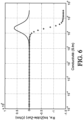
- An example of a relationship between the impedance variation ⁇ Z and the thickness e of target 4 is more precisely illustrated in Figure 5 .
- An example of a relationship between the impedance variation ⁇ Z and the conductivity of target 4 is more precisely illustrated in Figure Figure 6 .
- the solid line curve and the cross curve correspond respectively to the values of the real part and the imaginary part of the impedance variation ⁇ Z.
- the second set B comprising the inductor element 3 and the target 4 thus reflects or transmits part of the signal towards the ADC 2 of the first set A through the transmission line 5.
- the ADC 2 can thus measure the reflected or transmitted signal Y by the second set B.
- the reflected or transmitted signal Y is coupled via the coupling system 6, in particular the second coupling system 6b, to the ADC 2.
- the ADC 2 then transmits the received signal Y to the third set C.
- the third set C analyzes the transmitted signals X and received signals Y transmitted by the first set A and determines the ratio Y/X of the second set B over the frequency range ⁇ f .
- the Fourier transform ratio of the received signal Y with respect to the transmitted signal ⁇ , R Y / X
- the third set C comprises an analysis system 7.
- the analysis system 7 uses a model 8 linking the impedance variation ⁇ Z of the second set B to the conductivity of the target 4.
- the model 8 can in particular be approximated by calibration from a set of known conductivity targets 4, made up of different reference materials.
- the analysis system 7 determines the ratio Y/X from the transmitted signal impedance ⁇ Z, to deduce the conductivity of target 4 on the frequency range ⁇ f.
- the analysis system 7 of the third set C uses a model 8 of the electromagnetic interaction between the inducing element 3 and the target 4.
- the analysis system 7 then also includes a minimization algorithm .
- an initial theoretical input value of the conductivity of target 4 is transmitted into model 8, so that a theoretical impedance variation is deduced at different frequencies of the frequency range ⁇ f.
- These theoretical values of the impedance variation are compared to the measured experimental values of the impedance variation ⁇ Z determined by the analysis system 7 over the same frequency range ⁇ f.
- the difference is calculated and the conductivity input value of model 8 is adjusted step by step by iteration to minimize this difference.
- the conductivity of the semiconductor target 4 is thus determined. This iterative adjustment can also be carried out by comparing experimental Y/X ratio values with theoretical Y/X ratio values.
- a plurality of parameters of the target 4 It is for example possible to measure the conductivity(ies) and/or the thickness(es) of a target 4 comprising a multilayer material and/or inhomogeneous. Indeed, in modifying the frequency of the transmitted signal but may not be dependent on all layers of target 4. By varying the frequency of the emitted signal X and therefore the depth of penetration of the magnetic field H, it is possible to reconstruct a conductivity profile of target 4 for different layers of a multi-layer material or for different areas of a non-homogeneous material.
- these two parameters are initially estimated or selected randomly, then transmitted as initial input values in model 8 of the third set C.
- the measurements of the Y/X ratio for these two parameters for M different frequencies are then compared to the result of the experimental measurement for these M frequencies.
- the input values of model 8, in particular the thickness e and the conductivity, are then modified iteratively via the minimization algorithm until a stopping criterion is reached, for example until that the difference between the output values of model 8 and the result of experimental measurements is less than a predefined tolerance.
- the initial input values of model 8 can be chosen arbitrarily, in particular randomly.
- model 8 is adapted to converge towards final output values.
- the final output values of model 8 then provide an estimate of the thickness e and conductivity parameters of target 4.
- a single parameter namely the conductivity
- this measurement method can be generalized to N parameters to be determined and M measurement frequencies, with the number of measurement frequencies M greater than or equal to the number N of parameters to be determined. Furthermore, given that each measurement frequency M makes it possible to distinctly determine the real part and the imaginary part of a signal, it may also be possible to determine N parameters if the number of measurement frequencies M is greater than or equal to N /2 parameters to be determined.
- the boundary conditions in model 8 are adapted to target 4.
- the complete geometry of target 4 is in particular taken into account as values of model 8.
- the minimum thickness e of target 4 can be taken into account in the model 8 is, for example less than 1 ⁇ m, or even around 10nm.
- Distance 11 is also taken into account and compensated in model 8 to account for field losses.
- a target 4 can be tested in zones, in several times.
- the measurement sensitivity is optimal.
- optimal measurement sensitivity we mean that the Y/X ratio comprises a real part and/or an imaginary part varying respectively maximally around a particular measurement frequency.
- target 4 The lower the conductivity of target 4, the more necessary it is to use an emitted signal X having high frequencies to obtain optimal measurement sensitivity.
- the characterization of target 4 comprising layer(s) of low conductivity and low thickness will advantageously be improved with the use of an emitted signal X having high frequencies.
- a high conductivity of target 4 leads to a low variation in the Y/X ratio for high frequencies.
- the frequency range ⁇ f can be between 100kHz to 2 GHz, or even between 100kHz to 300MHz.
- a programmable logic circuit card (“field-programmable gate array” FPGA) or a fast processor coupled to digital/analog and fast analog/digital converters can be used to quickly scan a large frequency range ⁇ f.
- the conductivity of a large number of materials can be estimated by this method, such as silicon, as well as compounds like CIGS, CdTe, organic materials, new organic materials such as perovskytes, layers such as those based on III-V materials used in pn multi-junctions.
- the method is used to optimize multilayer/multi-junction surface treatments.
- the thickness(es) of the semiconductor materials of target 4 can be adapted for applications in electronics, in particular in the field of photovoltaics. These thicknesses usually vary from around 50nm to a few micrometers for thin layer materials, and from a few tens of micrometers to a few hundred micrometers for massive materials, such as crystalline silicon for example. Their conductivities can vary from 10 -3 Sm -1 to 10 4 Sm -1 . These conductivity values cover the typical range of conductivities of different types of semiconductor materials, in particular those used for photovoltaics, depending on whether they are in the form of thin layers, or in the form of self-supporting wafers.
- the device is for example used for non-destructive testing of material of target 4.
- the second set B and in particular the target 4 can be used in solution or embedded in ceramic to be used in environments under strong thermal or chemical constraints since a semiconductor is sensitive to surrounding conditions.
- target 4 can be used in a bath chemical.
- the measuring device makes it possible to measure the conductivity of target 4 in the dark.
- a measurement reference in the dark can in particular be used to allow a more sensitive measurement of the conductivity and/or the thickness e of targets 4 comprising one or more poorly photoconductive materials.
- the measuring device also makes it possible to measure the conductivity when the target 4, and in particular its first surface 4a and/or its second face 4b, is subjected to illumination.
- the measuring device can thus make it possible to measure conductivity values according to a time-dependent regime. According to this time-dependent regime, the conductivity values to which target 4 is subjected can be linked to the lifetime of the charge carriers of target 4.
- the measurement method can thus comprise an FGPA card or a fast processor coupled to digital/analog and fast analog/digital converters, as described above.
- An FPGA card makes it possible in particular to obtain a very fast measurement process making it possible to measure short life times of charge carriers of target 4 or to be integrated into a measurement chain.
- a treatment of a surface of the target 4, in particular of the first surface 4a, can be carried out to modify the life time of the charge carriers of the target 4.
Description
La présente invention est relative à la mesure sans contact de la conductivité de semi-conducteurs.The present invention relates to the non-contact measurement of the conductivity of semiconductors.
On connaît déjà usuellement des procédés de caractérisation sans contact de la conductivité de semi-conducteurs, utilisant un signal électrique monofréquentiel.We already know methods for contactless characterization of the conductivity of semiconductors, using a single-frequency electrical signal.
Par exemple, le document
La présente invention vise notamment à pallier ces inconvénients.The present invention aims in particular to overcome these drawbacks.
A cet effet, l'invention concerne un procédé de mesure sans contact de la conductivité de semi-conducteurs tel que défini par la revendication 1.To this end, the invention relates to a method for non-contact measurement of the conductivity of semiconductors as defined by
Un tel procédé de mesure permet notamment de caractériser la conductivité de nombreux types de matériaux en effectuant des mesures sur une large gamme de fréquences.Such a measurement method makes it possible in particular to characterize the conductivity of many types of materials by carrying out measurements over a wide range of frequencies.
Un tel procédé permet ainsi la caractérisation d'une large gamme de semi-conducteurs de conductivités différentes et d'épaisseurs différentes, et éventuellement de semi-conducteurs multicouches.Such a process thus allows the characterization of a wide range of semiconductors with different conductivities and different thicknesses, and possibly multilayer semiconductors.
En outre, un tel procédé permet de mesurer la conductivité de matériaux au cours de leur traitement, ce qui est notamment avantageux pour effectuer des contrôles qualités systématiques et par une méthode rapide dans des chaînes de production.In addition, such a method makes it possible to measure the conductivity of materials during their processing, which is particularly advantageous for carrying out systematic quality controls and by a rapid method in production lines.
Dans divers modes de réalisation du procédé selon l'invention, on peut éventuellement avoir recours en outre à l'une et/ou à l'autre des dispositions suivantes:
- le signal émis multi-fréquentiel est de la forme :

- le système d'analyse du troisième ensemble utilise un modèle reliant la variation d'impédance du deuxième ensemble à la conductivité de la cible, l'étape e) du procédé comprenant préalablement les étapes suivantes réalisées par le troisième ensemble :
- e1) à partir de la valeur du coefficient de réflexion ou de transmission, déterminer la variation d'impédance du deuxième ensemble sur la gamme de fréquences,
- e2) avec le modèle, en déduire la conductivité de la cible à partir de la variation d'impédance du deuxième ensemble ;
- le système d'analyse du troisième ensemble utilise un modèle de l'interaction électromagnétique entre l'élément inducteur et la cible semi-conductrice et un algorithme de minimisation, l'étape e) du procédé étant effectuée par méthode itérative selon les étapes suivantes :
- e'1) à partir de la valeur du coefficient de réflexion ou de transmission, déterminer la variation d'impédance du deuxième ensemble sur la gamme de fréquences,
- e'2) fournir une valeur d'entrée initiale de conductivité théorique de la cible dans le modèle,
- e'3) évaluer à partir du modèle la variation d'impédance du deuxième ensemble théorique pour la gamme de fréquences,
- e'4) évaluer la différence entre la variation d'impédance du deuxième ensemble théorique et la variation d'impédance du deuxième ensemble mesurée,
- e'5) minimiser ladite différence ;
- le procédé est adapté pour déterminer plusieurs conductivités simultanément d'une cible semi-conductrice multicouche ou pour la mesure de plusieurs cibles semi-conductrices ;
- le procédé est adapté pour déterminer l'épaisseur de chacune des couches de la cible semi-conductrice multicouche ;
- le premier ensemble comprend au moins un convertisseur numérique analogique, ledit convertisseur étant adapté pour émettre un signal multi-fréquentiel, le premier ensemble comprenant également un système d'acquisition convertisseur analogique numérique, ledit système d'acquisition étant adapté pour recevoir un signal multi-fréquentiel réfléchi ou transmis ;
- le premier ensemble comprend au moins un système de couplage, ledit système de couplage étant adapté pour coupler le signal émis par le convertisseur numérique analogique dans la ligne de transmission, et coupler le signal réfléchi ou transmis vers le système d'acquisition convertisseur analogique numérique ;
- le premier ensemble comprend au moins deux systèmes de couplage, un premier système de couplage étant adapté pour coupler le signal émis par le convertisseur numérique analogique dans une première ligne de transmission, et un deuxième système de couplage étant adapté pour coupler le signal réfléchi ou transmis dans une deuxième ligne de transmission vers le système d'acquisition convertisseur analogique numérique ;
- la gamme de fréquence du signal émis est comprise entre 100kHz et 300MHz ;
- la gamme de fréquence est choisie de sorte que les variations du coefficient de réflexion ou de transmission sont maximales pour une variation donnée de conductivité autour d'une fréquence de mesure particulière ; et
- le procédé utilise une gamme de fréquence élevée pour mesurer des conductivités faibles.
- the transmitted multi-frequency signal is of the form:
- the analysis system of the third set uses a model relating the impedance variation of the second set to the conductivity of the target, step e) of the method previously comprising the following steps carried out by the third set:
- e1) from the value of the reflection or transmission coefficient, determine the impedance variation of the second set over the frequency range,
- e2) with the model, deduce the conductivity of the target from the impedance variation of the second set;
- the analysis system of the third set uses a model of the electromagnetic interaction between the inducing element and the semiconductor target and a minimization algorithm, step e) of the method being carried out by iterative method according to the following steps:
- e'1) from the value of the reflection or transmission coefficient, determine the impedance variation of the second set over the frequency range,
- e'2) provide an initial input value of theoretical conductivity of the target in the model,
- e'3) evaluate from the model the impedance variation of the second theoretical set for the frequency range,
- e'4) evaluate the difference between the impedance variation of the second theoretical set and the impedance variation of the second measured set,
- e'5) minimize said difference;
- the method is suitable for determining several conductivities simultaneously of a multilayer semiconductor target or for measuring several semiconductor targets;
- the method is suitable for determining the thickness of each of the layers of the semiconductor target multi-layer;
- the first set comprises at least one digital-to-analog converter, said converter being adapted to emit a multi-frequency signal, the first set also comprising an analog-to-digital converter acquisition system, said acquisition system being adapted to receive a multi-frequency signal reflected or transmitted frequency;
- the first assembly comprises at least one coupling system, said coupling system being adapted to couple the signal emitted by the digital-to-analog converter into the transmission line, and to couple the signal reflected or transmitted to the analog-to-digital converter acquisition system;
- the first assembly comprises at least two coupling systems, a first coupling system being adapted to couple the signal transmitted by the digital-to-analog converter into a first transmission line, and a second coupling system being adapted to couple the reflected or transmitted signal in a second transmission line to the analog-digital converter acquisition system;
- the frequency range of the transmitted signal is between 100kHz and 300MHz;
- the frequency range is chosen so that the variations in the reflection or transmission coefficient are maximum for a given variation in conductivity around a particular measurement frequency; And
- the method uses a high frequency range to measure low conductivities.
L'invention concerne également un dispositif de mesure sans contact de la conductivité de semi-conducteur tel que défini par la revendication 11.The invention also relates to a device for non-contact measurement of semiconductor conductivity as defined by
Dans divers modes de réalisation du dispositif selon l'invention, on peut éventuellement avoir recours en outre à l'une et/ou à l'autre des dispositions suivantes:
- l'élément inducteur est imprimé sur un circuit, ledit circuit étant positionné à proximité de la cible semi-conductrice ; et
- l'élément inducteur est une bobine comprenant un rayon intérieur et un rayon extérieur, et dans lequel la cible s'étend dans un plan perpendiculaire à une direction principale de l'élément inducteur suivant deux dimensions, les rayons intérieur et extérieur de l'élément inducteur étant inférieurs aux dimensions de la cible, voire de l'ordre de la moitié des dimensions de la cible.
- the inductor element is printed on a circuit, said circuit being positioned near the semiconductor target; And
- the inductor element is a coil comprising a interior radius and an exterior radius, and in which the target extends in a plane perpendicular to a main direction of the inducing element along two dimensions, the interior and exterior radii of the inducing element being less than the dimensions of the target, or even around half the dimensions of the target.
D'autres caractéristiques et avantages de l'invention apparaîtront au cours de la description suivante d'une de ses formes de réalisation, donnée à titre d'exemple non limitatif, en regard des dessins joints :
- la
figure 1 représente schématiquement un premier mode de réalisation d'un dispositif de mesure de conductivité selon l'invention comprenant un premier ensemble, un deuxième ensemble et un troisième ensemble connecté au premier ensemble ; - la
figure 2 représente schématiquement un autre mode de réalisation du dispositif de mesure de conductivité selon l'invention comprenant un premier ensemble, un deuxième ensemble et un troisième ensemble connecté au premier ensemble ; - la
figure 3 représente schématiquement un autre mode de réalisation du dispositif de mesure de conductivité selon l'invention comprenant également un ensemble de référence connecté au premier ensemble ; - la
figure 4 représente une vue schématique en perspective du deuxième ensemble desfigures 1 et2 ; - la
figures 4A représente une vue schématique de côté du deuxième ensemble de lafigure 4 ; - la
figure 4B représente une vue schématique en coupe selon le plan IVB-IVB de lafigure 4A ; - la
figure 5 représente la partie réelle et la partie imaginaire de la variation d'impédance de l'élément inducteur en fonction de l'épaisseur de la cible ; - la
figure 6 représente la partie réelle et la partie imaginaire de la variation d'impédance de de l'élément inducteur en fonction de la conductivité de la cible ; - la
figure 7 représente la partie réelle du coefficient de réflexion en fonction de la fréquence du signal émis et de la conductivité de la cible ; et - la
figure 8 représente la partie imaginaire du coefficient de réflexion en fonction de la fréquence du signal émis et de la conductivité de la cible.
- there
figure 1 schematically represents a first embodiment of a conductivity measuring device according to the invention comprising a first assembly, a second assembly and a third assembly connected to the first assembly; - there
figure 2 schematically represents another embodiment of the conductivity measuring device according to the invention comprising a first assembly, a second assembly and a third assembly connected to the first assembly; - there
Figure 3 schematically represents another embodiment of the conductivity measuring device according to the invention also comprising a reference assembly connected to the first assembly; - there
Figure 4 represents a schematic perspective view of the second set offigures 1 And2 ; - there
figures 4A represents a schematic side view of the second set of theFigure 4 ; - there
Figure 4B represents a schematic sectional view according to plan IVB-IVB of theFigure 4A ; - there
figure 5 represents the real part and the imaginary part of the variation in impedance of the inducing element as a function of the thickness of the target; - there
Figure 6 represents the real part and the imaginary part of the impedance variation of the inducing element as a function of the conductivity of the target; - there
figure 7 represents the real part of the reflection coefficient as a function of the frequency of the transmitted signal and the conductivity of the target; And - there
figure 8 represents the imaginary part of the reflection coefficient as a function of the frequency of the transmitted signal and the conductivity of the target.
Sur les différentes figures, les mêmes références désignent des éléments identiques ou similaires.In the different figures, the same references designate identical or similar elements.
La conductivité d'une cible de matériau semi-conducteur 4 (appelé par la suite « cible ») est mesurée par la transmission d'un signal multi-fréquentiel dans un élément inducteur 3 de taille et de forme variables, par exemple une bobine 3, placée à proximité de la cible 4. La bobine 3 est par exemple réalisée sur un circuit imprimé inséré dans un circuit électronique. L'élément inducteur 3 a une hauteur h3 et s'étend entre une extrémité avant 3a et une extrémité arrière 3b. Par avant et arrière, on désigne ici respectivement l'extrémité de l'élément inducteur 3 la plus proche de la cible 4 et l'extrémité la plus éloignée de la cible 4. En variante, plusieurs éléments inducteurs 3, notamment des bobines 3, peuvent être utilisées, chaque élément inducteur 3 étant adapté pour une gamme de fréquence Δf.The conductivity of a target of semiconductor material 4 (hereinafter called "target") is measured by the transmission of a multi-frequency signal in an
Comme illustré sur la
Le premier ensemble A émet un signal X multi-fréquentiel vers le deuxième ensemble B le long de la ligne de transmission 5, et mesure le signal réfléchi ou transmis Y par le deuxième ensemble B vers le premier ensemble A le long de la ligne de transmission 5. Dans la suite, on désignera également le signal réfléchi ou transmis Y comme étant le signal reçu Y par le premier ensemble A.The first set A transmits a
Un troisième ensemble C est connecté au premier ensemble A. Les signaux émis X et reçu Y sont analysés par le troisième ensemble C. Le troisième ensemble C détermine le coefficient de réflexion ρ ou de transmission R (appelé par la suite « rapport Y/X ») du signal réfléchi ou transmis Y par rapport au signal émis X par le deuxième ensemble B. La conductivité de la cible 4 est ainsi déduite.A third set C is connected to the first set A. The signals transmitted ") of the reflected or transmitted signal Y in relation to the signal emitted X by the second set B. The conductivity of the
Plus particulièrement comme illustré sur la
En variante, comme illustré sur la
Selon une autre variante, comme illustré sur la
L'ensemble de référence R comprend un élément inducteur 3 identique à celui de deuxième ensemble B, notamment comme cela sera décrit ci-après. Toutefois, à la différence du deuxième ensemble B, l'ensemble de référence R ne comprend pas de cible 4. L'ensemble de référence R permet ainsi de mesurer le signal transmis ou réfléchi Y2 par l'élément inducteur 3 lorsque cet élément inducteur 3 se trouve en l'absence de la cible 4, c'est-à-dire lorsque l'élément inducteur 3 est uniquement entourée d'air à proximité. En variante, l'élément inducteur 3 de l'ensemble de référence R peut se trouver entouré d'un matériau de référence ou se trouver à proximité d'une cible de référence.The reference assembly R comprises an
Un bloc permet par la suite d'additionner, et notamment d'amplifier, le signal émis ou réfléchi Y par le deuxième ensemble B avec le signal émis ou réfléchi Y2 par l'ensemble de référence R. On obtient ainsi un signal final D tel que : ![]()
![]()
Avec A une constante d'amplification. En particulier, P est de préférence égal à π afin de réaliser une amplification différentielle entre les signaux Y et Y2. Le signal final D est ensuite transmis au premier ensemble A, et notamment vers ADC 2.With A an amplification constant. In particular, P is preferably equal to π in order to achieve differential amplification between the signals Y and Y2. The final signal D is then transmitted to the first set A, and in particular to
Dans le deuxième ensemble B, la cible de semi-conducteur 4 est située à proximité de l'élément inducteur 3. En particulier, la cible 4 s'étend dans un plan P perpendiculaire à une direction principale Z de l'élément inducteur 3 comme illustré par la
Comme représenté plus en détails sur les ![]()
![]()
Comme représenté plus en détails sur la
A titre d'exemple, pour une gamme de fréquences Δf comprise entre 1MHz et 50MHz, une bobine 3 ayant un rayon extérieur r2 de 3cm avec 5 spires peut être utilisée afin de mesurer la conductivité d'une cible 4 ayant un rayon r4 dans le plan P égale à environ 3 cm. Le nombre de spires de la bobine 3 peut notamment être réduit lors de l'utilisation de fréquences plus élevées.For example, for a frequency range Δf between 1MHz and 50MHz, a
Selon une autre réalisation représenté sur la
De cette façon, la cible 4, et notamment le champ magnétique induit Hi (comme expliqué ci-après), interagit avec l'élément inducteur 3. La distance 11 entre la cible 4 et l'élément inducteur 3 est alors par exemple de l'ordre de 1mm.In this way, the
La ligne de transmission 5 relie le premier ensemble A au deuxième ensemble B. La ligne de transmission 5 a une impédance caractéristique Zligne adaptée à l'impédance de sortie de l'ensemble A. La ligne de transmission 5 est par exemple une piste sur un circuit imprimé ou un câble coaxial ou un fil ou une ligne bifilaire.The
Le troisième ensemble C comprend un système d'analyse des données 7, le troisième ensemble C étant apte à analyser les données du signal émis X et du signal réfléchi ou transmis Y par le deuxième ensemble B. Le troisième ensemble C permet ainsi de déduire le rapport Y/X du signal reçu Y par le deuxième ensemble B par rapport au signal émis X, puis la conductivité de la cible 4.The third set C comprises a
Le fonctionnement du dispositif va maintenant être décrit plus en détails.The operation of the device will now be described in more detail.
Un signal multi-fréquentiel X est émis sur une gamme de fréquence Δf par le DAC 1 du premier ensemble A. Le signal est par exemple de la forme : 
Plus précisément, le signal émis X peut être de la forme : ![]()
![]()
![]()
![]()
Un tel signal émis X contient simultanément toutes les fréquences utiles à la caractérisation du deuxième ensemble B. En particulier, la durée minimale du signal émis X est fixée par sa fréquence fondamentale f1, plus précisément déterminée par ![]()
![]()
Il est alors possible de réaliser une mesure de la conductivité de la cible 4 sur un temps très court et d'observer des variations très rapides de la conductivité.It is then possible to measure the conductivity of
Les périodes du signal émis X peuvent être générées de manière continue ou par salve au cours du temps. Les périodes du signal reçu Y correspondant peuvent ainsi éventuellement être moyennées. Ceci permet également de caractériser l'évolution de la cible 4 au cours de temps, par exemple par analyse fréquentielle du type transformation de Fourier rapide (FFT) à fenêtre glissante.The periods of the transmitted signal X can be generated continuously or in bursts over time. The periods of the corresponding received signal Y can thus possibly be averaged. This also makes it possible to characterize the evolution of
En variante, le signal émis X peut être un signal dont la fréquence varie de manière séquentielle, par exemple avec une période de temps à une première fréquence fT1 puis une période de temps à une deuxième fréquence fT2, ou avec une fréquence fixe au cours du temps.Alternatively, the transmitted signal course of time.
Le dispositif de mesure permet donc de mesurer la conductivité de la cible 4 dans différents régimes, que ce soit en régime continu ou en régime dépendant du temps.The measuring device therefore makes it possible to measure the conductivity of the
Le signal émis X est couplé par l'intermédiaire du système de couplage 6, notamment du premier système de couplage 6a, à la ligne de transmission 5 afin d'être transmis à la ligne de transmission 5, notamment à la première ligne de transmission 5a. Le signal émis X est ainsi reçu par le deuxième ensemble B. Plus précisément, l'élément inducteur 3 du deuxième ensemble B est alimenté par le signal émis X.The transmitted signal . The transmitted signal
Comme illustré à la
La cible 4, qui est parcourue par les courants de Foucault 11, engendre un champ magnétique induit Hi et une variation d'impédance δZ du deuxième ensemble B. La variation d'impédance δZ consiste en la différence entre l'impédance Zcible de l'élément inducteur 3 en présence de la cible 4, et notamment en présence du champ magnétique induit Hi, et l'impédance Zair de l'élément inducteur 3 en l'absence de la cible 4, c'est-à-dire lorsque l'élément inducteur 3 est uniquement entourée d'air. Zair peut notamment être directement mesurée à partir des signaux X2, Y2 de l'ensemble de référence R de la 
A une fréquence et à une distance 11 entre l'élément inducteur 3 et la cible 4 donnée, la variation d'impédance δZ de la bobine 3 dépend donc de la conductivité et de l'épaisseur e de la cible 4 par l'intermédiaire de l'amplitude A0. Un exemple de relation entre la variation d'impédance δZ et l'épaisseur e de la cible 4 est plus précisément illustré à la
Du fait de cette variation d'impédance δZ, le deuxième ensemble B comprenant l'élément inducteur 3 et la cible 4 réfléchit ou transmet ainsi une partie du signal vers l'ADC 2 du premier ensemble A à travers la ligne de transmission 5.Due to this variation in impedance δZ, the second set B comprising the
L'ADC 2 peut ainsi mesurer le signal réfléchi ou transmis Y par le deuxième ensemble B. En particulier, le signal réfléchi ou transmis Y est couplé par l'intermédiaire du système de couplage 6, notamment du deuxième système de couplage 6b, à l'ADC 2.The
L'ADC 2 transmet alors le signal reçu Y au troisième ensemble C. Le troisième ensemble C analyse les signaux émis X et reçu Y transmis par le premier ensemble A et détermine le rapport Y/X du deuxième ensemble B sur la gamme de fréquences Δf. En particulier, le rapport de transformée de Fourier du signal reçu Y par rapport au signal émis X permet d'obtenir une mesure de ce rapport Y/X qui correspond soit à un coefficient de réflexion ρ, soit à un coefficient de transmission R en fréquence : ![]()
![]()
L'impédance Zcible du deuxième ensemble B, et notamment de l'élément inducteur 3, est reliée au rapport Y/X, exprimé dans le plan d'une section de la ligne de transmission 5, par la relation : ![]()
![]()
avec Zligne qui désigne l'impédance de la ligne de transmission 5 et Zcible l'impédance de l'élément inducteur 3. Il est ainsi possible à partir du rapport Y/X de déterminer la variation d'impédance δZ du deuxième ensemble B, et inversement.The target impedance Z of the second set B, and in particular of the ![]()
![]()
with Z line which designates the impedance of the
On décrit maintenant plus en détails le troisième ensemble C.We now describe the third set C in more detail.
Selon un premier mode de réalisation de l'invention, le troisième ensemble C comprend un système d'analyse 7. Le système d'analyse 7 utilise un modèle 8 reliant la variation d'impédance δZ du deuxième ensemble B à la conductivité de la cible 4. Le modèle 8 peut notamment être approximée par étalonnage à partir d'un ensemble de cibles 4 de conductivité connues, constituées de différents matériaux de référence.According to a first embodiment of the invention, the third set C comprises an
Le système d'analyse 7 détermine le rapport Y/X à partir du signal émis X et du signal reçu Y, puis détermine la variation d'impédance δZ du deuxième ensemble B. Le modèle 8 permet ensuite, à partir de cette variation d'impédance δZ, de déduire la conductivité de la cible 4 sur la gamme de fréquence Δf.The
Dans un second mode de réalisation, le système d'analyse 7 du troisième ensemble C utilise un modèle 8 de l'interaction électromagnétique entre l'élément inducteur 3 et la cible 4. Le système d'analyse 7 comprend alors également un algorithme de minimisation.In a second embodiment, the
Ainsi, une valeur théorique d'entrée initiale de la conductivité de la cible 4 est transmise dans le modèle 8, de sorte qu'une variation d'impédance théorique est déduite à différentes fréquences de la gamme de fréquence Δf. Ces valeurs théoriques de la variation d'impédance sont comparées aux valeurs expérimentales mesurées de la variation d'impédance δZ déterminées par le système d'analyse 7 sur la même gamme de fréquence Δf. La différence est calculée et la valeur d'entrée de conductivité du modèle 8 est ajustée de proche en proche par itération pour minimiser cette différence. La conductivité de la cible semi-conductrice 4 est ainsi déterminée. Cet ajustement itératif peut également être réalisé en comparant des valeurs des rapports Y/X expérimentales avec des valeurs de rapport Y/X théoriques.Thus, an initial theoretical input value of the conductivity of
En variante dans ce second mode de réalisation, on peut estimer à la fois la conductivité et l'épaisseur e d'une cible semi-conductrice par la méthode itérative.Alternatively, in this second embodiment, it is possible to estimate both the conductivity and the thickness e of a semiconductor target by the iterative method.
Toujours en variante, on peut estimer par la méthode itérative une pluralité de paramètres de la cible 4. Il est par exemple possible de mesurer la/les conductivités et/ou la/les épaisseurs d'une cible 4 comprenant un matériau multicouches et/ou non homogène. En effet, en modifiant la fréquence du signal émis X vers le deuxième ensemble B, il est possible de modifier l'épaisseur de pénétration du champ magnétique H dans la cible 4. Ainsi, le signal reçu Y est nécessairement dépendant de la première couche de la cible 4, mais peut ne pas être dépendant de toutes les couches de la cible 4. En faisant varier la fréquence du signal émis X et donc la profondeur de pénétration du champ magnétique H, il est possible de reconstruire un profil de conductivité de la cible 4 pour différentes couches d'un matériau multicouches ou pour différentes zones d'un matériau non homogène.Still as a variant, it is possible to estimate by the iterative method a plurality of parameters of the
Toujours selon ce second mode de réalisation, dans le cas par exemple d'une cible 4 monocouche dont on souhaite déterminer l'épaisseur e et la conductivité, ces deux paramètres sont initialement estimés ou sélectionnés aléatoirement, puis transmis comme valeurs d'entrée initiales dans le modèle 8 du troisième ensemble C. Les mesures du rapport Y/X pour ces deux paramètres pour M fréquences différentes sont alors comparées au résultat de la mesure expérimentale pour ces M fréquences.Still according to this second embodiment, in the case for example of a single-
Les valeurs d'entrée du modèle 8, notamment l'épaisseur e et la conductivité, sont alors modifiées de manière itérative via l'algorithme de minimisation jusqu'à l'atteinte d'un critère d'arrêt, par exemple jusqu'à ce que l'écart entre les valeurs de sortie du modèle 8 et le résultat de mesures expérimentales soit inférieur à une tolérance prédéfinie.
Les valeurs d'entrée initiales du modèle 8 peuvent être choisies arbitrairement, notamment aléatoirement. En particulier, le modèle 8 est adapté pour converger vers des valeurs de sortie finales. Les valeurs de sortie finales du modèle 8 fournissent alors une estimation des paramètres épaisseur e et conductivité de la cible 4. En particulier, dans le cas où la cible 4 est monocouche et d'épaisseur e connue, la situation est identique, un seul paramètre, à savoir la conductivité, étant à déterminer.The input values of
The initial input values of
De façon générale, ce procédé de mesure peut être généralisé à N paramètres à déterminer et M fréquences de mesures, avec le nombre de fréquences de mesure M supérieur ou égal au nombre N de paramètres à déterminer. En outre, étant donné que chaque fréquence de mesure M permet de déterminer distinctement la partie réelle et la partie imaginaire d'un signal, il peut être également possible de déterminer N paramètres si le nombre de fréquences de mesure M est supérieur ou égal à N/2 paramètres à déterminer.In general, this measurement method can be generalized to N parameters to be determined and M measurement frequencies, with the number of measurement frequencies M greater than or equal to the number N of parameters to be determined. Furthermore, given that each measurement frequency M makes it possible to distinctly determine the real part and the imaginary part of a signal, it may also be possible to determine N parameters if the number of measurement frequencies M is greater than or equal to N /2 parameters to be determined.
Les conditions aux limites dans le modèle 8 sont adaptées à la cible 4. La géométrie complète de la cible 4 est en particulier prise en compte comme valeurs du modèle 8. L'épaisseur e minimale de la cible 4 pouvant être prise en compte dans le modèle 8 est, par exemple inférieur à 1µm, voire de l'ordre de 10nm. La distance 11 est également prise en compte et compensé dans le modèle 8 pour tenir compte des pertes de champ.The boundary conditions in
Dans ce second mode de réalisation, on peut également envisager de mesurer plusieurs cibles 4 à la fois. En variante une cible 4 peut être testée par zones, en plusieurs fois.In this second embodiment, we can also consider measuring
Comme illustré sur les
A chaque conductivité de couche de la cible 4 à mesurer, il existe donc une gamme de fréquence Δf, notamment autour de la fréquence de mesure particulière, dans laquelle la sensibilité de mesure est maximale.For each layer conductivity of the
Plus la conductivité de la cible 4 est faible, plus il est nécessaire d'utiliser un signal émis X ayant des fréquences élevées pour obtenir une sensibilité de mesure optimale. Ainsi, la caractérisation de cible 4 comportant une/des couche(s) de faible conductivité et de faible épaisseur sera avantageusement améliorée avec l'utilisation d'un signal émis X ayant des fréquences élevées. De plus, une conductivité élevée de la cible 4 entraine une faible variation du rapport Y/X pour des fréquences élevées.The lower the conductivity of
La gamme de fréquences Δf peut être comprise entre 100kHz à 2 GHz, voire comprise entre 100kHz à 300MHz. Une carte circuit logique programmable (« field-programmable gâte array » FPGA) ou un processeur rapide couplé à des convertisseurs numérique/analogique et analogique/numérique rapide peuvent être utilisés pour balayer rapidement une grande gamme de fréquence Δf.The frequency range Δf can be between 100kHz to 2 GHz, or even between 100kHz to 300MHz. A programmable logic circuit card (“field-programmable gate array” FPGA) or a fast processor coupled to digital/analog and fast analog/digital converters can be used to quickly scan a large frequency range Δf.
La conductivité d'un grand nombre de matériaux peut être estimée par cette méthode, tels que le silicium, ainsi que des composés comme le CIGS, le CdTe, des matériaux organiques, de nouveaux matériaux organiques tels que des perovskytes, des couches telles que celles à base de matériaux III-V utilisées dans des multi-jonctions p-n. En variante, le procédé est utilisé pour optimiser des traitements de surface de multicouches/multi-jonctions.The conductivity of a large number of materials can be estimated by this method, such as silicon, as well as compounds like CIGS, CdTe, organic materials, new organic materials such as perovskytes, layers such as those based on III-V materials used in pn multi-junctions. Alternatively, the method is used to optimize multilayer/multi-junction surface treatments.
La ou les épaisseurs des matériaux semi-conducteurs de la cible 4 peuvent être adapté pour des applications en électronique, en particulier dans le domaine du photovoltaïque. Ces épaisseurs varient usuellement d'environ 50nm à quelques micromètres pour des matériaux en couches minces, et de quelques dizaines de micromètres à quelques centaines de micromètres pour des matériaux massifs, comme le silicium cristallin par exemple. Leurs conductivités peuvent varier de 10-3 S.m-1 à 104 S.m-1. Ces valeurs de conductivité recouvrent la gamme typique de conductivités des différents types de matériaux semi-conducteurs, en particulier ceux utilisés pour le photovoltaïque, selon qu'ils se présentent sous forme de couches minces, ou sous forme de plaquettes autosupportées.The thickness(es) of the semiconductor materials of
Le dispositif est par exemple utilisé pour le contrôle non destructif de matériau de la cible 4.The device is for example used for non-destructive testing of material of
En variante, le deuxième ensemble B, et notamment la cible 4, peut être utilisé en solution ou noyé dans de la céramique pour être utilisé dans des environnements sous fortes contraintes thermiques ou chimiques puisqu'un semi-conducteur est sensible aux conditions environnantes.Alternatively, the second set B, and in particular the
En variante, la cible 4 peut être utilisée en bain chimique.Alternatively,
Le dispositif de mesure permet de mesurer la conductivité de la cible 4 dans l'obscurité. Une référence de mesure à l'obscurité peut notamment être utilisée pour permettre une mesure plus sensible de la conductivité et/ou de l'épaisseur e de cibles 4 comportant un ou plusieurs matériaux peu photoconducteurs.The measuring device makes it possible to measure the conductivity of
Le dispositif de mesure permet également de mesurer la conductivité lorsque la cible 4, et notamment sa première surface 4a et/ou sa deuxième face 4b, est soumise à un éclairement. Dans le cas où la cible 4 est utilisée sous éclairement, le dispositif de mesure peut ainsi permettre de mesurer des valeurs de conductivité selon un régime dépendant du temps. Selon ce régime dépendant du temps, les valeurs de conductivité auquel est soumise la cible 4 peuvent être reliées à la durée de vie des porteurs de charge de la cible 4.The measuring device also makes it possible to measure the conductivity when the
Il est alors nécessaire que le procédé et le dispositif de mesure soit suffisamment rapide afin de détecter la durée de vie des porteurs de charges en régime dépendant du temps. Selon cette réalisation, le procédé de mesure peut ainsi comprendre une carte FGPA ou un processeur rapide couplé à des convertisseurs numérique/analogique et analogique/numérique rapide, comme décrits ci-dessus. Une carte FPGA permet notamment d'obtenir un procédé de mesure très rapide permettant de mesurer des temps de vie courts de porteurs de charge de la cible 4 ou d'être intégrée à une chaîne de mesure.It is then necessary that the method and the measuring device be sufficiently fast in order to detect the lifespan of the charge carriers in a time-dependent regime. According to this embodiment, the measurement method can thus comprise an FGPA card or a fast processor coupled to digital/analog and fast analog/digital converters, as described above. An FPGA card makes it possible in particular to obtain a very fast measurement process making it possible to measure short life times of charge carriers of
Ainsi, il est possible de combiner lors du procédé de mesure, l'émission d'un signal X tel que décrit ci-dessus avec un éclairement de la cible 4. Une telle combinaison permet notamment d'augmenter la sensibilité de la mesure de la conductivité de la cible 4, notamment pour une cible 4 multicouche.Thus, it is possible to combine during the process measurement, the emission of a
En outre, un traitement d'une surface de la cible 4, notamment de la première surface 4a, peut être réalisé pour modifier le temps de vie des porteurs de charge de la cible 4.In addition, a treatment of a surface of the
Bien évidemment, l'invention n'est pas limitée aux modes de réalisation décrits précédemment et fournis uniquement à titre d'exemple. Elle englobe diverses modifications, formes alternatives et autres variantes que pourra envisager l'homme du métier dans le cadre de la présente invention et notamment toutes combinaisons des différents modes de fonctionnement du dispositif et/ou du procédé décrits précédemment, pouvant être pris séparément ou en association.Obviously, the invention is not limited to the embodiments described above and provided solely by way of example. It encompasses various modifications, alternative forms and other variants that those skilled in the art may consider in the context of the present invention and in particular all combinations of the different modes of operation of the device and/or the method described above, which can be taken separately or in combination. association.
Claims (13)
- A method for contactless measurement of the conductivity of semiconductors, said method being implemented by:- a first assembly (A) comprising a signal (X, Y) transmission/reception system able to transmit/receive a multi-frequency signal (X, Y) over a frequency range (Δf), the multi-frequency signal (X) transmitted being in the form:
 - a second assembly (B) comprising at least one semiconducting target (4) and a single inductor element (3), the semiconducting target (4) being positioned in proximity to the inductor element (3),- a transmission line (5), said transmission line (5) being adapted to transmit the signal (X, Y) between the first assembly (A) and the second assembly (B), and- a third assembly (C), said third assembly (C) being intended to be connected to the first assembly (A), the third assembly (C) comprising an analysis system (7), the third assembly (C) being able to analyse a signal (X) transmitted by the first assembly (A) and a reflected or transmitted signal (Y) received by the first assembly (A), and the third assembly (C) being able to deduce a reflection or transmission coefficient (ρ, R) of the transmitted signal (X) therefrom,said method comprising at least the following steps:a) the first assembly (A) transmits a multi-frequency signal (X),b) the second assembly (B) reflects or transmits at least one part of the multi-frequency signal (X) transmitted by the first assembly (A),c) the first assembly (A) receives the multi-frequency signal (Y) reflected or transmitted by the second assembly (B),d) the third assembly (C) calculates the reflection or transmission coefficient (ρ, R) of the signal (X) transmitted for the frequency range (Δf) from the ratio of the signal transmitted by the first assembly (A) to the signal reflected or transmitted by the second assembly (B),e) the third assembly (C) determines conductivity of the semiconducting target (4) using the impedance variation over the frequency range (Δf) of the second assembly (B) obtained from said ratio.
 - The non-contact measurement method according to claim 1, wherein the analysis system (7) of the third assembly (C) uses a model (8) relating the impedance variation (δZ) of the second assembly (B) to the conductivity of the target (4), step e) of the method comprising beforehand the following steps performed by the third assembly (C):e1) from the value of the reflection or transmission coefficient (ρ, R), determining the impedance variation (δZ) of the second assembly (B) over the frequency range (Δf),e2) using model (8), deduce conductivity of the target from the impedance variation (δZ) of the second assembly (B) therefrom.
- The non-contact measurement method according to claim 1, wherein the analysis system (7) of the third assembly (C) uses a model (8) of electromagnetic interaction between the inductor element (3) and the semiconducting target (4) and a minimisation algorithm, step e) of the method being carried out iteratively according to the following steps:e'1) from the value of the reflection or transmission coefficient (ρ, R), determining the impedance variation (δZ) of the second assembly (B) over the frequency range (Δf),e'2) providing an initial input value of theoretical conductivity of the target (4) in the model (8),e'3) evaluating from the model (8) the theoretical impedance variation (δZ) of the second assembly (B) for the frequency range (Δf),e'4) evaluating the difference between the theoretical impedance variation (5Z) of the second assembly (B) and the measured impedance variation (δZ) of the second assembly (B),e'5) minimising said difference.
- The non-contact measurement method according to claim 3, adapted to determine simultaneously several conductivities of a multilayer semiconducting target (4) or to measure several semiconducting targets (4).
- The non-contact measurement method according to claim 4, adapted to determine the thickness (e) of each of the layers of the multilayer semiconducting target (4).
- The non-contact measurement method according to any of the preceding claims, wherein the first assembly (A) comprises at least one analogue digital converter (1), said converter being adapted to transmit the multi-frequency signal (X), the first assembly (A) also comprising an analogue digital converter acquisition system (2), said acquisition system (2) being adapted to receive the multi-frequency reflected or transmitted signal (Y).
- The non-contact measurement method according to claim 6, wherein the first assembly (A) comprises at least one coupling system (6), said coupling system (6) being adapted to couple the signal (X) transmitted by the digital analogue converter (1) in the transmission line (5), and to couple the signal reflected or transmitted (Y) to the analogue digital converter acquisition system (2).
- The non-contact measurement method according to claim 6, wherein the first assembly (A) comprises at least two coupling systems (6), a first coupling system (6a) being adapted to couple the signal transmitted (X) by the digital analogue converter (1) in a first transmission line (5a), and a second coupling system (6b) being adapted to couple the signal reflected or transmitted (Y) in a second transmission line (5b) to the digital analogue converter acquisition system (2).
- The non-contact measurement method according to any of the preceding claims, wherein the frequency range (Δf) of the transmitted signal (X) is between 100 kHz and 300 MHz.
- The non-contact measurement method according to any of the preceding claims, wherein the frequency range (Af) is chosen so that the variations in the reflection or transmission coefficient (ρ, R) are maximum for a given variation in conductivity around a particular measurement frequency.
- A device for non-contact measurement of the conductivity of a semiconductor, characterised in that it comprises:- a first assembly (A), said first assembly (A) being a signal (X, Y) transmission/reception system able to transmit/receive a multi-frequency signal (X, Y) over a frequency range (Δf), the multi-frequency signal (X) transmitted being in the form:
 - a second assembly (B), said second assembly (B) comprising at least one semiconducting target (4) and a single inductor element (3), the semiconducting target (4) being positioned in proximity to the inductor element (3),- at least one transmission line (5), said transmission line (5) being adapted to transmit the signal (X, Y) between the first assembly (A) and the second assembly (B),- a third assembly (C), said third assembly (C) being intended to be connected to the first assembly (A), the third assembly (C) comprising an analysis system (7), the third assembly (C) being able to analyse a transmitted signal (X) and a reflected or transmitted signal (Y) received by the first assembly (A) and the third assembly (C) being able to deduce therefrom a reflection or transmission coefficient (ρ, R) of the transmitted signal (X) for the frequency range (Δf) from the ratio of the signal transmitted by the first assembly (A) to the signal reflected or transmitted by the second assembly (B) and to determine conductivity of the semiconducting target (4) using the impedance variation over the frequency range (Δf) of the second assembly (B) obtained from said ratio.
 - The non-contact measurement device according to claim 11, wherein the inductor element (3) is printed on a circuit, said circuit being positioned in proximity to the semiconducting target (4).
- The non-contact measurement device according to any of claims 11 and 12, wherein the inductor element (3) is a coil comprising an internal radius (r1) and an external radius (r2), and wherein the semiconducting target (4) extends in a plane (P) perpendicular to a main direction (Z) of the inductor element (3) along two dimensions (L1, L2), the internal and external radii (r1, r2) of the inductor element (3) being less than the dimensions (L1, L2) of the semiconducting target (4), or even in the order of half the dimensions (L1, L2) of the target (4).
Applications Claiming Priority (2)
| Application Number | Priority Date | Filing Date | Title |
|---|---|---|---|
| FR1553392A FR3035224B1 (en) | 2015-04-16 | 2015-04-16 | CONTACTLESS MEASUREMENT OF SEMICONDUCTOR CONDUCTIVITY |
| PCT/FR2016/050800 WO2016166449A1 (en) | 2015-04-16 | 2016-04-07 | Contactless measurement of the conductivity of semiconductors |
Publications (2)
| Publication Number | Publication Date |
|---|---|
| EP3283891A1 EP3283891A1 (en) | 2018-02-21 |
| EP3283891B1 true EP3283891B1 (en) | 2024-03-13 |
Family
ID=53366157
Family Applications (1)
| Application Number | Title | Priority Date | Filing Date |
|---|---|---|---|
| EP16721874.2A Active EP3283891B1 (en) | 2015-04-16 | 2016-04-07 | Contactless measurement of the conductivity of semiconductors |
Country Status (4)
| Country | Link |
|---|---|
| US (1) | US10429435B2 (en) |
| EP (1) | EP3283891B1 (en) |
| FR (1) | FR3035224B1 (en) |
| WO (1) | WO2016166449A1 (en) |
Families Citing this family (1)
| Publication number | Priority date | Publication date | Assignee | Title |
|---|---|---|---|---|
| CN106771849B (en) * | 2016-11-15 | 2019-07-26 | 中国电子科技集团公司第四十一研究所 | The test method of two impedance discontinuity point reflections response on a kind of transmission line |
Citations (1)
| Publication number | Priority date | Publication date | Assignee | Title |
|---|---|---|---|---|
| US4303885A (en) * | 1979-06-18 | 1981-12-01 | Electric Power Research Institute, Inc. | Digitally controlled multifrequency eddy current test apparatus and method |
Family Cites Families (7)
| Publication number | Priority date | Publication date | Assignee | Title |
|---|---|---|---|---|
| US4286215A (en) * | 1979-05-18 | 1981-08-25 | Bell Telephone Laboratories, Incorporated | Method and apparatus for the contactless monitoring carrier lifetime in semiconductor materials |
| US6369603B1 (en) * | 1997-09-02 | 2002-04-09 | Midwest Research Institute | Radio frequency coupling apparatus and method for measuring minority carrier lifetimes in semiconductor materials |
| JP4265206B2 (en) * | 2002-11-27 | 2009-05-20 | 株式会社 東北テクノアーチ | Non-contact conductivity measurement system |
| IL153894A (en) * | 2003-01-12 | 2010-05-31 | Nova Measuring Instr Ltd | Method and system for thickness measurements of thin conductive layers |
| US8633700B1 (en) * | 2013-03-05 | 2014-01-21 | Hunt Energy Enterprises, Llc | Sensors for passive electroseismic and seismoelectric surveying |
| US9887587B2 (en) * | 2014-09-11 | 2018-02-06 | Cpg Technologies, Llc | Variable frequency receivers for guided surface wave transmissions |
| US9564861B2 (en) * | 2014-10-31 | 2017-02-07 | Nxp Usa, Inc. | Broadband radio frequency power amplifiers, and methods of manufacture thereof |
-
2015
- 2015-04-16 FR FR1553392A patent/FR3035224B1/en active Active
-
2016
- 2016-04-07 WO PCT/FR2016/050800 patent/WO2016166449A1/en active Application Filing
- 2016-04-07 EP EP16721874.2A patent/EP3283891B1/en active Active
- 2016-04-07 US US15/566,792 patent/US10429435B2/en active Active
Patent Citations (1)
| Publication number | Priority date | Publication date | Assignee | Title |
|---|---|---|---|---|
| US4303885A (en) * | 1979-06-18 | 1981-12-01 | Electric Power Research Institute, Inc. | Digitally controlled multifrequency eddy current test apparatus and method |
Also Published As
| Publication number | Publication date |
|---|---|
| FR3035224A1 (en) | 2016-10-21 |
| FR3035224B1 (en) | 2018-08-31 |
| WO2016166449A1 (en) | 2016-10-20 |
| EP3283891A1 (en) | 2018-02-21 |
| US20180100887A1 (en) | 2018-04-12 |
| US10429435B2 (en) | 2019-10-01 |
Similar Documents
| Publication | Publication Date | Title |
|---|---|---|
| EP0064908B1 (en) | Process and device to measure the temperature of a body with microwaves | |
| CA2777036C (en) | Device for measuring wind speed | |
| EP2602598B1 (en) | Bolometric detector for electromagnetic radiation in the terahertz spectral band and detector matrix comprising such detectors | |
| EP1982202B1 (en) | Electrically-modulatable extended light source and a measurement device for characterising a semiconductor including one such source | |
| EP2472215B1 (en) | Method and device for the neutralisation of a target | |
| FR2851662A1 (en) | Medium e.g. linear probe, discontinuity detecting method for e.g. portable medical apparatus, involves applying coherence criteria to selected maxima for regrouping maxima to same discontinuity, where maxima has value higher than threshold | |
| EP3749949B1 (en) | Terahertz reflection imaging system | |
| EP3234638A1 (en) | Method for determining parameters of a compression filter and associated multichannel radar | |
| EP3283891B1 (en) | Contactless measurement of the conductivity of semiconductors | |
| CA2419079A1 (en) | Method and device for measuring a line attenuation | |
| WO1992014164A1 (en) | Method for measuring the temperature of a material by using microwave radiation | |
| EP3325985B1 (en) | Device for electromagnetic dosimetry and associated method | |
| WO2015036398A1 (en) | Method for the non-destructive ultrasonic testing of a part by echo analysis | |
| EP1671140A1 (en) | Magnetic-field-measuring device | |
| CA2881524A1 (en) | Analogue amplification device intended in particular for a laser anemometer | |
| EP2932236B1 (en) | Photoreflectance device | |
| FR3020526A1 (en) | METHOD FOR GENERATING M DEMODULATION SIGNALS | |
| FR2933914A1 (en) | VEHICLE SEAT HEADREST EQUIPPED WITH ADJUSTMENT DEVICE | |
| EP3237924B1 (en) | Method for measuring a direction of incidence of an incident wave for an instantaneous wideband receiver and associated receiver | |
| EP3877773B1 (en) | System for analysing faults by reflectometry of optimised dynamic range | |
| WO2002046780A1 (en) | Device for electromagnetic characterisation of a tested structure | |
| EP4184158A1 (en) | Detection of burns during the machining of a mechanical part by eddy current method | |
| WO2018020148A1 (en) | Method and device for measuring the thickness of a metallic coating | |
| WO2021099727A1 (en) | Method for detecting defects by focusing laser-pulse-generated ultrasonic waves | |
| FR2972055A1 (en) | Method for determination of row of distance ambiguity of echo signal received by Doppler type pulsed radar, involves determining row of distance ambiguity of echo signal from one of three frequency spectrums |
Legal Events
| Date | Code | Title | Description |
|---|---|---|---|
| STAA | Information on the status of an ep patent application or granted ep patent |
Free format text: STATUS: THE INTERNATIONAL PUBLICATION HAS BEEN MADE |
|
| PUAI | Public reference made under article 153(3) epc to a published international application that has entered the european phase |
Free format text: ORIGINAL CODE: 0009012 |
|
| STAA | Information on the status of an ep patent application or granted ep patent |
Free format text: STATUS: REQUEST FOR EXAMINATION WAS MADE |
|
| 17P | Request for examination filed |
Effective date: 20171020 |
|
| AK | Designated contracting states |
Kind code of ref document: A1 Designated state(s): AL AT BE BG CH CY CZ DE DK EE ES FI FR GB GR HR HU IE IS IT LI LT LU LV MC MK MT NL NO PL PT RO RS SE SI SK SM TR |
|
| AX | Request for extension of the european patent |
Extension state: BA ME |
|
| DAV | Request for validation of the european patent (deleted) | ||
| DAX | Request for extension of the european patent (deleted) | ||
| RAP1 | Party data changed (applicant data changed or rights of an application transferred) |
Owner name: ECOLE SUPERIEURE D'ELECTRICITE Owner name: CNRS CENTRE NATIONAL DE LA RECHERCHE SCIENTIFIQUE Owner name: UNIVERSITE PARIS-SACLAY |
|
| STAA | Information on the status of an ep patent application or granted ep patent |
Free format text: STATUS: EXAMINATION IS IN PROGRESS |
|
| 17Q | First examination report despatched |
Effective date: 20210615 |
|
| STAA | Information on the status of an ep patent application or granted ep patent |
Free format text: STATUS: EXAMINATION IS IN PROGRESS |
|
| RAP3 | Party data changed (applicant data changed or rights of an application transferred) |
Owner name: ECOLE SUPERIEURE D'ELECTRICITE Owner name: UNIVERSITE PARIS-SACLAY Owner name: CNRS CENTRE NATIONAL DE LA RECHERCHE SCIENTIFIQUE |
|
| GRAP | Despatch of communication of intention to grant a patent |
Free format text: ORIGINAL CODE: EPIDOSNIGR1 |
|
| STAA | Information on the status of an ep patent application or granted ep patent |
Free format text: STATUS: GRANT OF PATENT IS INTENDED |
|
| RIC1 | Information provided on ipc code assigned before grant |
Ipc: H01L 21/66 20060101ALI20231005BHEP Ipc: G01R 31/28 20060101ALI20231005BHEP Ipc: G01R 31/311 20060101ALI20231005BHEP Ipc: G01R 31/265 20060101ALI20231005BHEP Ipc: G01R 31/26 20140101ALI20231005BHEP Ipc: G01R 27/06 20060101AFI20231005BHEP |
|
| INTG | Intention to grant announced |
Effective date: 20231020 |
|
| GRAS | Grant fee paid |
Free format text: ORIGINAL CODE: EPIDOSNIGR3 |
|
| GRAA | (expected) grant |
Free format text: ORIGINAL CODE: 0009210 |
|
| STAA | Information on the status of an ep patent application or granted ep patent |
Free format text: STATUS: THE PATENT HAS BEEN GRANTED |
|
| AK | Designated contracting states |
Kind code of ref document: B1 Designated state(s): AL AT BE BG CH CY CZ DE DK EE ES FI FR GB GR HR HU IE IS IT LI LT LU LV MC MK MT NL NO PL PT RO RS SE SI SK SM TR |
|
| REG | Reference to a national code |
Ref country code: GB Ref legal event code: FG4D Free format text: NOT ENGLISH |
|
| REG | Reference to a national code |
Ref country code: CH Ref legal event code: EP |
|
| REG | Reference to a national code |
Ref country code: DE Ref legal event code: R096 Ref document number: 602016086269 Country of ref document: DE |
|
| GRAT | Correction requested after decision to grant or after decision to maintain patent in amended form |
Free format text: ORIGINAL CODE: EPIDOSNCDEC |