EP3280226A1 - Method and arrangement for providing flicker-free light with two output channels - Google Patents
Method and arrangement for providing flicker-free light with two output channels Download PDFInfo
- Publication number
- EP3280226A1 EP3280226A1 EP16182738.1A EP16182738A EP3280226A1 EP 3280226 A1 EP3280226 A1 EP 3280226A1 EP 16182738 A EP16182738 A EP 16182738A EP 3280226 A1 EP3280226 A1 EP 3280226A1
- Authority
- EP
- European Patent Office
- Prior art keywords
- current
- output
- colour
- channel
- emitting means
- Prior art date
- Legal status (The legal status is an assumption and is not a legal conclusion. Google has not performed a legal analysis and makes no representation as to the accuracy of the status listed.)
- Withdrawn
Links
- 238000000034 method Methods 0.000 title claims description 16
- 230000009467 reduction Effects 0.000 claims abstract description 63
- 239000004065 semiconductor Substances 0.000 claims abstract description 23
- 230000008859 change Effects 0.000 claims description 4
- 238000001228 spectrum Methods 0.000 description 14
- 230000007423 decrease Effects 0.000 description 7
- 238000013459 approach Methods 0.000 description 5
- 239000003086 colorant Substances 0.000 description 4
- 230000000694 effects Effects 0.000 description 4
- 230000005457 Black-body radiation Effects 0.000 description 2
- 241000282412 Homo Species 0.000 description 2
- 230000035559 beat frequency Effects 0.000 description 2
- 238000006243 chemical reaction Methods 0.000 description 2
- 238000012937 correction Methods 0.000 description 2
- 230000008878 coupling Effects 0.000 description 2
- 238000010168 coupling process Methods 0.000 description 2
- 238000005859 coupling reaction Methods 0.000 description 2
- 238000000295 emission spectrum Methods 0.000 description 2
- 230000010355 oscillation Effects 0.000 description 2
- 239000007787 solid Substances 0.000 description 2
- 230000002411 adverse Effects 0.000 description 1
- 230000032683 aging Effects 0.000 description 1
- 239000003990 capacitor Substances 0.000 description 1
- 238000004891 communication Methods 0.000 description 1
- 238000010276 construction Methods 0.000 description 1
- 230000003247 decreasing effect Effects 0.000 description 1
- 230000001419 dependent effect Effects 0.000 description 1
- 238000005265 energy consumption Methods 0.000 description 1
- 230000006870 function Effects 0.000 description 1
- 230000010354 integration Effects 0.000 description 1
- 238000013507 mapping Methods 0.000 description 1
- 239000011159 matrix material Substances 0.000 description 1
- 238000005259 measurement Methods 0.000 description 1
- 238000012986 modification Methods 0.000 description 1
- 230000004048 modification Effects 0.000 description 1
- 230000003287 optical effect Effects 0.000 description 1
- 238000005457 optimization Methods 0.000 description 1
- 230000008569 process Effects 0.000 description 1
- 238000012545 processing Methods 0.000 description 1
- 230000000392 somatic effect Effects 0.000 description 1
- 230000036962 time dependent Effects 0.000 description 1
Images

Classifications
-
- H—ELECTRICITY
- H05—ELECTRIC TECHNIQUES NOT OTHERWISE PROVIDED FOR
- H05B—ELECTRIC HEATING; ELECTRIC LIGHT SOURCES NOT OTHERWISE PROVIDED FOR; CIRCUIT ARRANGEMENTS FOR ELECTRIC LIGHT SOURCES, IN GENERAL
- H05B45/00—Circuit arrangements for operating light-emitting diodes [LED]
- H05B45/20—Controlling the colour of the light
-
- H—ELECTRICITY
- H05—ELECTRIC TECHNIQUES NOT OTHERWISE PROVIDED FOR
- H05B—ELECTRIC HEATING; ELECTRIC LIGHT SOURCES NOT OTHERWISE PROVIDED FOR; CIRCUIT ARRANGEMENTS FOR ELECTRIC LIGHT SOURCES, IN GENERAL
- H05B45/00—Circuit arrangements for operating light-emitting diodes [LED]
- H05B45/50—Circuit arrangements for operating light-emitting diodes [LED] responsive to malfunctions or undesirable behaviour of LEDs; responsive to LED life; Protective circuits
- H05B45/59—Circuit arrangements for operating light-emitting diodes [LED] responsive to malfunctions or undesirable behaviour of LEDs; responsive to LED life; Protective circuits for reducing or suppressing flicker or glow effects
-
- H—ELECTRICITY
- H05—ELECTRIC TECHNIQUES NOT OTHERWISE PROVIDED FOR
- H05B—ELECTRIC HEATING; ELECTRIC LIGHT SOURCES NOT OTHERWISE PROVIDED FOR; CIRCUIT ARRANGEMENTS FOR ELECTRIC LIGHT SOURCES, IN GENERAL
- H05B45/00—Circuit arrangements for operating light-emitting diodes [LED]
- H05B45/30—Driver circuits
- H05B45/37—Converter circuits
-
- H—ELECTRICITY
- H05—ELECTRIC TECHNIQUES NOT OTHERWISE PROVIDED FOR
- H05B—ELECTRIC HEATING; ELECTRIC LIGHT SOURCES NOT OTHERWISE PROVIDED FOR; CIRCUIT ARRANGEMENTS FOR ELECTRIC LIGHT SOURCES, IN GENERAL
- H05B45/00—Circuit arrangements for operating light-emitting diodes [LED]
- H05B45/30—Driver circuits
- H05B45/395—Linear regulators
Definitions
- the invention relates to using semiconductor light sources to provide lighting that is controllable with respect to at least intensity and possibly also colour and/or colour temperature.
- the invention relates to avoiding visible flickering of the lights.
- PWM dimming where the acronym PWM comes from pulse width modulation. Basically it means switching the semiconductor light source on and off rapidly enough so that the human eye does not recognize the changes but only perceives the mean intensity of lighting that depends on the on/off duty cycle.
- PFM pulse frequency modulation
- PDM pulse density modulation
- PWM dimming is used as a general designation of all dimming schemes that utilize rapid on/off switching to achieve a perceived mean intensity.
- Methods for reducing the output current of a driver device to implement PWM dimming can be generally designated as pulse-based current reduction.
- the number and relative weights of higher frequency components needed to accurately model the PWM pulse train depend on how steep and sharp the flanks of the PWM pulses are.
- the sum of two PWM dimmed light streams is the sum of two such sums and thus contains a complicated matrix of oscillations at a large number of frequencies.
- the interference between two light sources has prominent significance in the generation of so-called tunable white light.
- White LEDs of two different colour temperatures can be driven at different relative intensities, so that the resultant light appears to have a colour temperature that is the weighted sum of the original colour temperatures of the different light sources.
- Using exactly the same PWM frequency for both of them might help to mitigate some interference problems, but the synchronization must be very good, because already a difference of 1 Hz creates a beat frequency with one constructive-interference peak and one destructive-interference valley per second, which is easily perceivable to a human observer.
- the objects of the invention are achieved with a hybrid dimming strategy in which constant current reduction is used in each channel between the maximum intensity and a threshold, and PWM dimming is used between the threshold and a minimum intensity, so that it becomes unlikely that both channels would be in the PWM dimming range simultaneously.
- a driver device for semiconductor light-emitting means comprising:
- a luminaire comprising a driver device of the kind described above and semiconductor light-emitting means coupled to receive the controllable output current from said first output channel and said second output channel.
- a method for generating controllable output current simultaneously for first semiconductor light-emitting means of first colour and second semiconductor light-emitting means of second colour comprising:
- Fig. 1 illustrates schematically a driver device 101 for semiconductor light-emitting means 102 and 103.
- the driver device comprises a first output channel 104 and a second output channel 105.
- the output channels 104 and 105 are essentially controllable current sources.
- the first output channel 104 is configured to provide a controllable output current lout1 for light-emitting means 102 of first colour.
- said first colour is so-called cool white, i.e. white light the spectrum of which resembles the visible part of blackbody radiation from an object the surface temperature of which is relatively high, such as 6500K.
- the second output channel 105 is configured to provide a controllable output current lout2 for light-emitting means 103 of second colour.
- said second colour is so-called warm white, i.e. white light the spectrum of which resembles the visible part of blackbody radiation from an object the surface temperature of which is significantly lower, such as 2700K.
- These colours and colour temperatures are used for the sake of example, and any other colours or colour temperatures could be used instead.
- the first and second colours may even be the same colour unless it is explicitly said that they are different colours.
- the driver device 101 comprises a control unit 106 that is configured to receive colour setting commands, and a power conversion unit 107 that receives mains power and distributes it in appropriate form to the first 104 and second 105 output channels.
- the power conversion unit 107 may comprise e.g. an input section with EMI filter(s) and rectifier(s), and a PFC (power factor correction) section that comprises one or more switched-mode power supplies for synchronizing the current drawn from the mains power with the voltage waveform of the mains power.
- colour setting command is used as a general designation of all kinds of machine-readable or machine-executable instructions that indicate to the control unit 106 the characteristics of a combined emission spectrum that should be produced by using the semiconductor light-emitting means that the control unit 106 has at its disposal.
- the semiconductor light-emitting means are white LEDs of two different colour temperatures
- a colour setting command may be a command to produce white light at a characteristic colour temperature that is at or between the extremes set by the characteristic colour temperatures of the component light sources 102 and 103.
- the effective electric current through each light-emitting means defines the emission intensity at the respective colour, and the combined emission spectrum is the weighted sum of the component spectra, where the weights are the relative magnitudes of the effective electric currents.
- the control unit 106 is configured to set the simultaneous output currents lout1 and lout2 of the first 104 and second 105 output channels to match a received colour setting command.
- the control unit 106 may comprise e.g. one or more processors programmed to carry out the necessary functions.
- a control interface 108 is provided so that the control unit 106 may receive the colour setting commands from a remote device.
- the control interface 108 may conform to a standard of a building automation system, so that the colour setting commands can be created and distributed with a central controlling device that follows that standard.
- the standard may be part 209 of the standard IEC 62386, so that the colour setting commands may be so-called DALI Type 8 commands.
- the control interface 108 may alternatively or additionally comprise a wireless interface, so that the control unit 106 may receive colour setting commands conforming to e.g. the Bluetooth, Bluetooth Low Energy, ZigBee, WLAN, IrDA, or NFC standards or to some other commonly used communications standards.
- the driver device 101 comprises an outer cover, so that circuitry of the first output channel 104, the second output channel 105, and the control unit 106 are all inside the outer cover.
- Electric connectors 109 and 110 are provided that are accessible from outside the outer cover for making connections to the light-emitting means 102 and 103 of first and second colour.
- the semiconductor light-emitting means 102 and 103 may be provided in one or more so-called LED modules, which are essentially circuit boards the surface of which serves both as an attachment surface of the LEDs and as a carrier of conductive tracks through which the electric currents flow to and from the LEDs.
- an integrated driver and LED module is built, having a common circuit board so that at least part of the circuitry of the first output channel 104, second output channel 105, and control unit 106 is located on the same circuit board on which at least a part of the light-emitting means 102 and 103 are also located.
- Each of the first 104 and second 105 output channels is capable of both constant current reduction and pulse-based current reduction.
- Constant current reduction means that the amperage of a steadily flowing output current is reduced
- pulse-based current reduction means producing rapidly repeated pulses of output current and reducing the portion of time when output current flows in relation to the portion of time when output current doesn't flow.
- pulse-based current reduction may take the form of e.g. pulse width modulation, pulse frequency modulation, or pulse density modulation.
- Circuits that are capable of reducing current are naturally also capable of increasing current by performing an opposite operation; for example pulse-based current increasing means producing rapidly repeated pulses of output current and increasing the portion of time when output current flows in relation to the portion of time when output current doesn't flow.
- the driver device is configured to apply so-called hybrid dimming in both the first 104 and the second 105 output channel.
- Hybrid dimming means that constant current reduction is used for at least one range of desired output intensities and pulse-based current reduction is used for at least another range of desired output intensities. Said ranges may be adjacent and non-overlapping on the intensity axis, but they may also overlap partly or wholly.
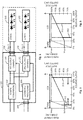
- Fig. 2 illustrates a non-overlapping hybrid dimming scheme in which an output current of a channel is set through constant current reduction between a maximum (100% output intensity) and a threshold value (here: 20% output intensity), and through pulse-based current reduction (here: PWM) between said threshold value and a minimum (0% intensity).
- the solid curve in fig. 2 shows how the peak current (which is synonymous to the amperage of the steadily flowing output current when duty cycle is 100%) decreases from its maximum value Imax to a smaller value Imin linearly when the output intensity of the corresponding channel decreases from 100% to 20%, and remains constant at said value Imin in the output intensity range between 20% and 0%.
- the dotted curve in fig. 2 shows how the duty cycle remains at 100% when the output intensity of the corresponding channel decreases from 100% to 20%, and decreases linearly from 100% to 0% when the output intensity decreases from 20% to 0%.
- a first output channel has been set to 10% output intensity and the second channel has been set to 90% output intensity, as shown by the vertical lines 201 and 202 respectively.
- the output current produced by the first output channel comes at peak value Imin and duty cycle 50%, while the output current produced by the second output channel comes at a peak value only slightly below the maximum output current Imax and duty cycle 100%. Since only one of the channels is applying pulse-based current reduction (the other having 100% duty cycle), there can be no interference between PWM frequencies, and flicker is thus avoided.
- the control unit 106 of the driver device 101 is configured to implement changes in set colour at least through reciprocal changes in the output currents of the first 104 and second channels 105.
- An example of such reciprocal changes is illustrated by the single-ended horizontal arrows in fig. 2 : the intensity of the first output channel is increased and the intensity of the second output channel is decreased.
- Fig. 3 shows how, as a result of said reciprocal change, the first output channel has been set to 30% intensity and the second output channel has been set to 70% intensity, as shown by the vertical lines 301 and 302 respectively. None of the channels is applying pulse-based current reduction, so there can be no interference between PWM frequencies and flicker is again avoided.
- the sum of the channel-specific intensities is 100% in each of figs. 2 and 3 , meaning that the combined light output is not dimmed, only its colour (or colour temperature) is changed.
- the first channel in the examples above is the 6500K channel and the second channel is the 2700K channel of fig. 1
- the combined output spectrum corresponds to white light at 3080K in fig. 2 (calculated as 0.1*6500K + 0.9*2700K) and white light at 3840K in fig. 3 (calculated as 0.3*6500K + 0.7*2700K), at full overall intensity.
- Dimming the combined light output may result in a situation in which the channel-specific intensity of each channel is below 20%, so both channels may be in the pulse-based current reduction range. In that case there is the possibility of interference-based flicker. However, since the overall intensity of the combined output spectrum is relatively low in such a case, the possible flicker may be more difficult to perceive and it may have less somatic effects than if flicker occurred at full or nearly full overall intensity.
- the exemplary threshold value 20% has been used above, but it may be larger or smaller, for example 10%.
- a threshold value can be selected for example on the basis of energy consumption and colour consistency: if the efficiency of the output channels can be kept at good level and if the low current does not cause much distortion in the spectrum of emitted light, the threshold value can be relatively small. Correspondingly if the efficiency of the output channels suffers significantly and/or the emitted colour suffers from heavy distortion at lower peak current levels, it is advisable to select a larger threshold value.
- the control unit receives the colour setting commands (and possibly intensity setting commands) that define the desired values of T(and E ). It may then calculate the channel-specific intensities E i using equations (1) and (2). If there are more than 2 channels, there may be several possible values for the E i that lead to the desired characteristic colour temperature T and relative intensity E of the combined output spectrum. In that case the control unit may utilize a suitable optimization algorithm, for example so that it aims at keeping each selected E i value as small as possible to reduce the generation of heat in each channel. It is also possible that the selection of available colour temperatures T of the combined output spectrum is limited, for example because the available set of command words for colour temperature is limited.
- the optimal E i values for each desired characteristic colour temperature T at 100% output intensity may have been calculated beforehand and stored in a table in the memory of the control unit.
- the E i values to be used are then obtained by scaling the stored values with the desired overall relative output intensity E .
- Fig. 4 illustrates a driver device for semiconductor light-emittting means according to an embodiment.
- the first block on the main power line is the input section 401, which comprises rectifier and filter functionalities and produces a DC (or rectified AC) voltage between the lines VDC and GND.
- the next block is the PFC (power factor correction) block 402, which may comprise a suitably controlled switched-mode power supply or some other kind of PFC functionality.
- the DC/DC converter block 403 produces the so-called bus voltage between the lines VBUS and 0V, to which the parallel output channels or output stages 404 and 405 are coupled. Additionally the DC/DC converter block 403 produces an auxiliary voltage level on line VCC, which is also coupled to the output channels or output stages 404 and 405.
- a monitor circuit and soft start functionality 406 may control the operation of the PFC 402 and DC/DC converter block 403.
- a microcontroller 407 and an output current setting block 408 represent schematically one or more processors and associated circuits that constitute the control unit of the driver device in fig. 4 .
- Some examples of associated circuits are explicitly shown, like a sensor functionality (NTC; negative temperature coefficient; meaning a temperature sensor) 409 and a control bus interface 410.
- NTC negative temperature coefficient
- a control bus interface 410 Included in the schematically shown microcontroller 407 but not explicitly illustrated in fig. 4 is a program memory for storing one or more sets of machine-readable instructions that constitute the program to be executed by said one or more processors. Executing said machine-readable instructions cause the implementation of the method(s) according to embodiment(s) of the invention.
- the output current setting block 408 may comprise for example an amplifier based coupling that includes an external connection, to which an external current setting resistor can be connected for setting the maximum output current to be produced by any of the two output channels.
- Such couplings are well known in the art of LED drivers and do not need to be described here in more detail. If the auxiliary voltage VCC is not needed in the output channels, it may be just for providing an operating voltage to some active circuit(s) in the output current setting block 408.
- Control connections from the blocks 407 and 408 that constitute the control unit to the output channels 404 and 405 comprise the ISET and CTRL lines in fig. 4 .
- One exemplary ways of using such control lines is such where the commands to set the actual output currents of the output channels come through the CTRL1 and CTRL2 lines respectively, while the ISET lines serve to set the maximum output current (also known as Imax in the description earlier).
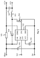
- Fig. 5 illustrates a simplified example of a circuit that can be used for example as one of the output channels 404 and 405 in the driver device of fig. 4 .
- the circuit of fig. 5 is essentially a switched-mode power supply for generating the output current of the respective output channel. It comprises a current switch, which here is a MOSFET 501, as well as a switch driver circuit 502 configured to provide switching pulses to the current switch at a switching frequency.
- the switch driver circuit 502 is most advantageously an integrated circuit.
- Other typical components of the switched-mode power supply are an inductor 503, a freewheeling diode 504, a current sensing resistor 505 and a number of capacitors 506, 507, and 508.
- a special feature of the circuit of fig. 5 is that the output current it produces can be set through constant current reduction and through pulse-based current reduction using a single control input 509 of the switch driver circuit 502.
- a switch driver circuit is for example the MP24894 circuit available from Monolithic Power Systems, San Jose, California.
- the value of the first threshold is 0.3 V
- the value of the second threshold is 2.7 V.
- a voltage smaller than 0.3 V between the driver circuit's input pin marked EN and the ground potential pin GND keeps the MP24894 from giving any switching pulses at all, while a voltage larger than 0.3 V but smaller than 2.7 V enables it to give switching pulses but simultaneously limits the peak current between a minimum value and a maximum value so that the closer the voltage is to 2.7 V the closer the peak current can be to the maximum value.
- control unit should contain a control pulse formatter coupled to the control input 509 and configured to provide said control input with control pulses of variable amplitude exceeding or meeting said first threshold at a pulse width modulation frequency that is smaller than the switching frequency mentioned above.
- a control pulse formatter may be implemented e.g. as a programmed executable process within the microcontroller block 407 in fig. 4 , or as a separate circuit element consisting analogue and/or digital components.
- the output channel implements pulse-based current reduction at the PWM frequency and the minimum peak current value. Setting the output current through constant current reduction necessitates maintaining the control input 509 at the appropriate voltage between 0.3 V and 2.7 V (where maintaining is conceptually the same as PWM with 100% duty cycle).
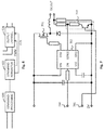
- Fig. 6 illustrates conceptually a slightly different approach in which there are two control signals to the output channel 601: one for setting the output current through constant current reduction (CCR) and another for setting the output current through pulse-based current reduction (PWM).
- the two control signals could come directly from two different outputs of a processor, but in fig. 6 it is assumed that there is a command formatter 602 that produces the control signals from one control command received from a command processing unit 603.
- the circuit is essentially a switched-mode power supply for generating the output current of the respective output channel. It comprises a current switch 701 and a switch driver circuit 702 configured to provide switching pulses to said current switch at a switching frequency.
- the switch driver circuit 702 has an enabling control input labelled EN in fig. 7 , and is configured to respond to voltages exceeding an enabling threshold at said control input (to be more accurate, between the control input EN and the ground potential pin GND) by enabling the generation of switching pulses.
- the circuit comprises also a current feedback circuit 703 for the switch driver circuit 702.
- the switch driver circuit 702 is configured to respond to signals provided by said current feedback circuit 703 by controlling at least one of the length, the frequency, or the duty cycle of the switching pulses.
- the command formatter is coupled to the enabling control input through line 704 and configured to provide the control input with control pulses at a pulse width modulation frequency that is smaller than the switching frequency mentioned above. Effectively the control pulses repetitively enable and disable the operation of the output channel, thus implementing pulse-based current reduction.
- the command formatter is also configured to provide the current feedback circuit 703 with a gain control signal through line 705.
- the gain control signal is effective to change a feedback gain of the current feedback circuit 703. In the implementation of fig. 7 the gain control signal changes the conductivity of a bipolar transistor, which in turn controls the flow of currents through the branches of the resistor network from which the current feedback signal is taken to the appropriate input pin of the switch driver circuit 702.
- a luminaire comprises a driver device according to one of the embodiments described so far, as well as semiconductor light-emitting means coupled to receive the controllable output current from the first output channel and the second output channel.
- the aim of the method is to generate controllable output current simultaneously for first semiconductor light-emitting means of first colour and second semiconductor light-emitting means of second colour.
- the method comprises receiving a colour setting command and resolving how the currents through the first and second light-emitting means are to be set to match said colour setting command.
- Said resolving may be accomplished for example by calculating or by using the received colour setting command as a key to a look-up table from which the appropriate commands and/or parameters are read for setting the currents through the first and second light-emitting means.
- the method comprises setting one of the currents through the first and second light-emitting means through constant current reduction and the other through pulse-based current reduction.
- the current to be set through constant current reduction is the one for channel-specific intensity between a maximum and threshold value and the current to be set through pulse-based current reduction is the one for channel-specific intensity between said threshold value and a minimum.
- the threshold value of relative intensity defines a sharp division between a PWM domain (lower intensities) and a CCR domain (higher intensities), but there can be a range of intermediate relative intensities within which both constant current reduction and pulse-based current reduction are applied.
- the arrangement can be equipped with optical feedback that measures the actual emitted intensity and/or colour and/or colour temperature of light, either for each channel separately or for the combined output spectrum, so that the result of the measurement may fine tune the channel-specific relative intensities to achieve the desired combined output spectrum as accurately as possible.
- the mapping between colour commands and channel-specific peak currents and/or duty cycles may comprise time-dependent factors that compensate for effects caused by the ageing of the LEDs.
- a flicker detector may be employed that detects interference-based flicker and e.g. changes the threshold value at which pulse-based current reduction changes to constant current reduction, so that the threshold may dynamically take into account the actual occurrence of flicker.
Landscapes
- Circuit Arrangement For Electric Light Sources In General (AREA)
Abstract
Description
- The invention relates to using semiconductor light sources to provide lighting that is controllable with respect to at least intensity and possibly also colour and/or colour temperature. In particular the invention relates to avoiding visible flickering of the lights.
- Semiconductor light sources, such as light-emitting diodes (or LEDs for short) respond extremely fast to changes in the amount of electric current flowing through them by changing the amount of emitted light in a corresponding way. This phenomenon is utilized in so-called PWM dimming, where the acronym PWM comes from pulse width modulation. Basically it means switching the semiconductor light source on and off rapidly enough so that the human eye does not recognize the changes but only perceives the mean intensity of lighting that depends on the on/off duty cycle. Depending on the details of what is changed the method may be called PFM (pulse frequency modulation), PDM (pulse density modulation) or something else, but the principle of rapidly toggling between two extreme values, changing some characteristic of the toggling and obtaining a resultant change in mean value is common to them all. In this description the term PWM dimming is used as a general designation of all dimming schemes that utilize rapid on/off switching to achieve a perceived mean intensity. Methods for reducing the output current of a driver device to implement PWM dimming can be generally designated as pulse-based current reduction.
- Although the natural integration tendency of the human eye would allow using PWM frequencies of 100 Hz or even less, it has been observed that flicker at even unperceivably high frequencies may have subconscious effects on humans. At the time of writing this description it is believed that the frequency-dependent effects of PWM dimming are bound to the modulation percentage. The so-called Lehman/Wilkins flicker risk graph is widely adopted, stating that the minimum PWM frequency should be at least 1.25 kHz at 100% modulation depth. The recommended minimum PWM frequency decreases linearly in a log-log graph of modulation depth versus frequency so that 100 Hz suffices at 3% modulation depth.
- When two or more PWM dimmed LED light sources are present in the same space, one must consider not only the PWM frequencies of the individual light sources but also interference phenomena. In an oversimplified case if the intensities of two individual light sources oscillated according to purely sinusoidal curves of frequencies f1 and f2, the observed sum intensity would have the so-called beat frequency f = f1-f2 (the sum frequency f1+f2 is also present, but since it is higher than any of the component PWM frequencies, it has little importance). The intensity of real PWM dimmed light equals a sum of infinitely many sinusoidal oscillations, in which the frequency of the lowest order component equals the PWM frequency. The number and relative weights of higher frequency components needed to accurately model the PWM pulse train depend on how steep and sharp the flanks of the PWM pulses are. The sum of two PWM dimmed light streams is the sum of two such sums and thus contains a complicated matrix of oscillations at a large number of frequencies.
- The interference between two light sources has prominent significance in the generation of so-called tunable white light. White LEDs of two different colour temperatures can be driven at different relative intensities, so that the resultant light appears to have a colour temperature that is the weighted sum of the original colour temperatures of the different light sources. Using exactly the same PWM frequency for both of them might help to mitigate some interference problems, but the synchronization must be very good, because already a difference of 1 Hz creates a beat frequency with one constructive-interference peak and one destructive-interference valley per second, which is easily perceivable to a human observer. It would be highly desirable to be able to produce a tunable white luminaire (or, more generally, a two-or-more-channel luminaire with differently coloured channels) without the risk of flicker, without adverse effects caused by interference, and without the need for complicated hardware.
- It is an objective of the present invention to provide a driver device, a luminaire, and a method for generating controllable output current that mitigate the risk of flicker when two or more channels are in use for driving semiconductor light-emitting means.
- The objects of the invention are achieved with a hybrid dimming strategy in which constant current reduction is used in each channel between the maximum intensity and a threshold, and PWM dimming is used between the threshold and a minimum intensity, so that it becomes unlikely that both channels would be in the PWM dimming range simultaneously.
- According to an aspect of the invention there is provided a driver device for semiconductor light-emitting means, comprising:
- a first output channel for providing a controllable output current for light-emitting means of first colour, said first output channel being configured for both constant current reduction and pulse-based current reduction,
- a second output channel for providing a controllable output current for light-emitting means of second colour, said second output channel being configured for both constant current reduction and pulse-based current reduction, and
- a control unit configured to receive colour setting commands, to set simultaneous output currents of said first and second output channels to match a received colour setting command, and to implement changes in set colour at least through reciprocal changes in said output currents;
- According to another aspect of the invention there is provided a luminaire comprising a driver device of the kind described above and semiconductor light-emitting means coupled to receive the controllable output current from said first output channel and said second output channel.
- According to yet another aspect of the invention there is provided a method for generating controllable output current simultaneously for first semiconductor light-emitting means of first colour and second semiconductor light-emitting means of second colour, the method comprising:
- receiving a colour setting command and resolving how the currents through the first and second light-emitting means are to be set to match said colour setting command,
- setting one of the currents through the first and second light-emitting means through constant current reduction and the other through pulse-based current reduction, wherein the current to be set through constant current reduction is the one between a maximum and threshold value and the current to be set through pulse-based current reduction is the one between said threshold value and a minimum, and
- implementing changes in set colour through reciprocal changes in said currents.
- The exemplifying embodiments of the invention presented in this patent application are not to be interpreted to pose limitations to the applicability of the appended claims. The verb "to comprise" and its derivatives are used in this patent application as an open limitation that does not exclude the existence of features that are not recited. The features described hereinafter are mutually freely combinable unless explicitly stated otherwise.
- The novel features which are considered as characteristic of the invention are set forth in particular in the appended claims. The invention itself, however, both as to its construction and its method of operation, together with additional objects and advantages thereof, will be best understood from the following detailed description of specific embodiments when read in connection with the accompanying drawings.
-
-
Figure 1 illustrates a two-channel driver device and associated semiconductor light-emitting means, -
figure 2 illustrates dimming curves and settings for one colour temperature, -
figure 3 illustrates dimming curves and settings for another colour temperature, -
figure 4 illustrates functional blocks of a two-channel driver device, -
figure 5 illustrates a switched-mode power supply that can be used in an output channel, -
figure 6 illustrates the use of a command formatter, and -
figure 7 illustrates a switched-mode power supply that can be used in an output channel when a command formatter is in use. -
Fig. 1 illustrates schematically adriver device 101 for semiconductor light-emitting means 102 and 103. The driver device comprises afirst output channel 104 and asecond output channel 105. Theoutput channels first output channel 104 is configured to provide a controllable output current lout1 for light-emitting means 102 of first colour. In this example it is assumed that said first colour is so-called cool white, i.e. white light the spectrum of which resembles the visible part of blackbody radiation from an object the surface temperature of which is relatively high, such as 6500K. Thesecond output channel 105 is configured to provide a controllable output current lout2 for light-emitting means 103 of second colour. In this example it is assumed that said second colour is so-called warm white, i.e. white light the spectrum of which resembles the visible part of blackbody radiation from an object the surface temperature of which is significantly lower, such as 2700K. These colours and colour temperatures are used for the sake of example, and any other colours or colour temperatures could be used instead. The first and second colours may even be the same colour unless it is explicitly said that they are different colours. - Additionally the
driver device 101 comprises acontrol unit 106 that is configured to receive colour setting commands, and apower conversion unit 107 that receives mains power and distributes it in appropriate form to the first 104 and second 105 output channels. Thepower conversion unit 107 may comprise e.g. an input section with EMI filter(s) and rectifier(s), and a PFC (power factor correction) section that comprises one or more switched-mode power supplies for synchronizing the current drawn from the mains power with the voltage waveform of the mains power. - The concept "colour setting command" is used as a general designation of all kinds of machine-readable or machine-executable instructions that indicate to the
control unit 106 the characteristics of a combined emission spectrum that should be produced by using the semiconductor light-emitting means that thecontrol unit 106 has at its disposal. Taken the example offig. 1 , in which the semiconductor light-emitting means are white LEDs of two different colour temperatures, a colour setting command may be a command to produce white light at a characteristic colour temperature that is at or between the extremes set by the characteristic colour temperatures of thecomponent light sources control unit 106 is configured to set the simultaneous output currents lout1 and lout2 of the first 104 and second 105 output channels to match a received colour setting command. Thecontrol unit 106 may comprise e.g. one or more processors programmed to carry out the necessary functions. - A
control interface 108 is provided so that thecontrol unit 106 may receive the colour setting commands from a remote device. Thecontrol interface 108 may conform to a standard of a building automation system, so that the colour setting commands can be created and distributed with a central controlling device that follows that standard. As an example the standard may be part 209 of the standard IEC 62386, so that the colour setting commands may be so-called DALI Type 8 commands. Thecontrol interface 108 may alternatively or additionally comprise a wireless interface, so that thecontrol unit 106 may receive colour setting commands conforming to e.g. the Bluetooth, Bluetooth Low Energy, ZigBee, WLAN, IrDA, or NFC standards or to some other commonly used communications standards. - The use of solid and dashed outlines in
fig. 1 illustrate two alternative structural approaches that are common at the time of writing this description. According to a first approach thedriver device 101 comprises an outer cover, so that circuitry of thefirst output channel 104, thesecond output channel 105, and thecontrol unit 106 are all inside the outer cover.Electric connectors means means first output channel 104,second output channel 105, andcontrol unit 106 is located on the same circuit board on which at least a part of the light-emittingmeans - Each of the first 104 and second 105 output channels is capable of both constant current reduction and pulse-based current reduction. Constant current reduction means that the amperage of a steadily flowing output current is reduced, while pulse-based current reduction means producing rapidly repeated pulses of output current and reducing the portion of time when output current flows in relation to the portion of time when output current doesn't flow. As described in the background section, pulse-based current reduction may take the form of e.g. pulse width modulation, pulse frequency modulation, or pulse density modulation. Circuits that are capable of reducing current are naturally also capable of increasing current by performing an opposite operation; for example pulse-based current increasing means producing rapidly repeated pulses of output current and increasing the portion of time when output current flows in relation to the portion of time when output current doesn't flow.
- The driver device is configured to apply so-called hybrid dimming in both the first 104 and the second 105 output channel. Hybrid dimming means that constant current reduction is used for at least one range of desired output intensities and pulse-based current reduction is used for at least another range of desired output intensities. Said ranges may be adjacent and non-overlapping on the intensity axis, but they may also overlap partly or wholly.
-
Fig. 2 illustrates a non-overlapping hybrid dimming scheme in which an output current of a channel is set through constant current reduction between a maximum (100% output intensity) and a threshold value (here: 20% output intensity), and through pulse-based current reduction (here: PWM) between said threshold value and a minimum (0% intensity). The solid curve infig. 2 shows how the peak current (which is synonymous to the amperage of the steadily flowing output current when duty cycle is 100%) decreases from its maximum value Imax to a smaller value Imin linearly when the output intensity of the corresponding channel decreases from 100% to 20%, and remains constant at said value Imin in the output intensity range between 20% and 0%. The dotted curve infig. 2 shows how the duty cycle remains at 100% when the output intensity of the corresponding channel decreases from 100% to 20%, and decreases linearly from 100% to 0% when the output intensity decreases from 20% to 0%. - In
fig. 2 a first output channel has been set to 10% output intensity and the second channel has been set to 90% output intensity, as shown by thevertical lines duty cycle 100%. Since only one of the channels is applying pulse-based current reduction (the other having 100% duty cycle), there can be no interference between PWM frequencies, and flicker is thus avoided. - The
control unit 106 of thedriver device 101 is configured to implement changes in set colour at least through reciprocal changes in the output currents of the first 104 andsecond channels 105. An example of such reciprocal changes is illustrated by the single-ended horizontal arrows infig. 2 : the intensity of the first output channel is increased and the intensity of the second output channel is decreased.Fig. 3 shows how, as a result of said reciprocal change, the first output channel has been set to 30% intensity and the second output channel has been set to 70% intensity, as shown by thevertical lines - The sum of the channel-specific intensities is 100% in each of
figs. 2 and 3 , meaning that the combined light output is not dimmed, only its colour (or colour temperature) is changed. Assuming that the first channel in the examples above is the 6500K channel and the second channel is the 2700K channel offig. 1 , the combined output spectrum corresponds to white light at 3080K infig. 2 (calculated as 0.1*6500K + 0.9*2700K) and white light at 3840K infig. 3 (calculated as 0.3*6500K + 0.7*2700K), at full overall intensity. Dimming the combined light output may result in a situation in which the channel-specific intensity of each channel is below 20%, so both channels may be in the pulse-based current reduction range. In that case there is the possibility of interference-based flicker. However, since the overall intensity of the combined output spectrum is relatively low in such a case, the possible flicker may be more difficult to perceive and it may have less somatic effects than if flicker occurred at full or nearly full overall intensity. - For the last-mentioned reason it is advisable to maintain the threshold value between constant current reduction and pulse-based current reduction relatively small. The
exemplary threshold value 20% has been used above, but it may be larger or smaller, for example 10%. A threshold value can be selected for example on the basis of energy consumption and colour consistency: if the efficiency of the output channels can be kept at good level and if the low current does not cause much distortion in the spectrum of emitted light, the threshold value can be relatively small. Correspondingly if the efficiency of the output channels suffers significantly and/or the emitted colour suffers from heavy distortion at lower peak current levels, it is advisable to select a larger threshold value. - A more general mathematical description can be formulated for a dimming strategy of the kind discussed above for output channels driving white LEDs of different colour temperature. Let us use the following designations:
- N
- number of output channels controlled in parallel,
- Ti
- characteristic colour temperature of the i:th output channel; i ∈ [1, N],
- T
- characteristic colour temperature of the combined output spectrum,
- di
- duty cycle of the pulse-based current reduction on the i:th output channel; di ∈ [0, 100],
- Ii
- peak current on the i:th output channel; Ii ∈ [Imin, Imax],
- Ei
- relative intensity of the light emitted by the LEDs in the i:th channel; Ei ∈ [0, 100],
- Eth
- threshold of relative intensity below which pulse-based current reduction is used and above which constant current reduction is used; Eth ∈ [0, 100],
- E
- relative intensity of the combined output spectrum; also called the dimming ratio; E ∈ [0, 100].
- The characteristic colour temperature of the combined output spectrum is the weighted sum


- The control unit receives the colour setting commands (and possibly intensity setting commands) that define the desired values of T(and E). It may then calculate the channel-specific intensities Ei using equations (1) and (2). If there are more than 2 channels, there may be several possible values for the Ei that lead to the desired characteristic colour temperature T and relative intensity E of the combined output spectrum. In that case the control unit may utilize a suitable optimization algorithm, for example so that it aims at keeping each selected Ei value as small as possible to reduce the generation of heat in each channel. It is also possible that the selection of available colour temperatures T of the combined output spectrum is limited, for example because the available set of command words for colour temperature is limited. In such a case the optimal Ei values for each desired characteristic colour temperature T at 100% output intensity may have been calculated beforehand and stored in a table in the memory of the control unit. The Ei values to be used are then obtained by scaling the stored values with the desired overall relative output intensity E.
- Once the channel-specific intensity value Ei has been selected, the peak current Ii for that channel can be chosen according to


-
Fig. 4 illustrates a driver device for semiconductor light-emittting means according to an embodiment. The first block on the main power line is theinput section 401, which comprises rectifier and filter functionalities and produces a DC (or rectified AC) voltage between the lines VDC and GND. The next block is the PFC (power factor correction) block 402, which may comprise a suitably controlled switched-mode power supply or some other kind of PFC functionality. The DC/DC converter block 403 produces the so-called bus voltage between the lines VBUS and 0V, to which the parallel output channels oroutput stages DC converter block 403 produces an auxiliary voltage level on line VCC, which is also coupled to the output channels oroutput stages soft start functionality 406 may control the operation of thePFC 402 and DC/DC converter block 403. - A
microcontroller 407 and an outputcurrent setting block 408 represent schematically one or more processors and associated circuits that constitute the control unit of the driver device infig. 4 . Some examples of associated circuits are explicitly shown, like a sensor functionality (NTC; negative temperature coefficient; meaning a temperature sensor) 409 and acontrol bus interface 410. Included in the schematically shownmicrocontroller 407 but not explicitly illustrated infig. 4 is a program memory for storing one or more sets of machine-readable instructions that constitute the program to be executed by said one or more processors. Executing said machine-readable instructions cause the implementation of the method(s) according to embodiment(s) of the invention. - The output
current setting block 408 may comprise for example an amplifier based coupling that includes an external connection, to which an external current setting resistor can be connected for setting the maximum output current to be produced by any of the two output channels. Such couplings are well known in the art of LED drivers and do not need to be described here in more detail. If the auxiliary voltage VCC is not needed in the output channels, it may be just for providing an operating voltage to some active circuit(s) in the outputcurrent setting block 408. - Control connections from the
blocks output channels fig. 4 . One exemplary ways of using such control lines is such where the commands to set the actual output currents of the output channels come through the CTRL1 and CTRL2 lines respectively, while the ISET lines serve to set the maximum output current (also known as Imax in the description earlier). -
Fig. 5 illustrates a simplified example of a circuit that can be used for example as one of theoutput channels fig. 4 . The circuit offig. 5 is essentially a switched-mode power supply for generating the output current of the respective output channel. It comprises a current switch, which here is aMOSFET 501, as well as aswitch driver circuit 502 configured to provide switching pulses to the current switch at a switching frequency. Theswitch driver circuit 502 is most advantageously an integrated circuit. Other typical components of the switched-mode power supply are aninductor 503, afreewheeling diode 504, acurrent sensing resistor 505 and a number ofcapacitors - A special feature of the circuit of
fig. 5 is that the output current it produces can be set through constant current reduction and through pulse-based current reduction using asingle control input 509 of theswitch driver circuit 502. This requires only that theswitch driver circuit 502 is configured to respond to voltages exceeding a first threshold at saidcontrol 509 input by enabling the providing of switching pulses and to voltages between said first threshold and a second, further threshold at thecontrol input 509 by allowing an amplitude of a measured current to reach a value proportional to the voltage at thecontrol input 509. At the time of writing this description such a switch driver circuit is for example the MP24894 circuit available from Monolithic Power Systems, San Jose, California. In the MP24894 the value of the first threshold is 0.3 V, and the value of the second threshold is 2.7 V. Thus a voltage smaller than 0.3 V between the driver circuit's input pin marked EN and the ground potential pin GND keeps the MP24894 from giving any switching pulses at all, while a voltage larger than 0.3 V but smaller than 2.7 V enables it to give switching pulses but simultaneously limits the peak current between a minimum value and a maximum value so that the closer the voltage is to 2.7 V the closer the peak current can be to the maximum value. - Using a circuit like that in
fig. 5 as an output channel means that the control unit should contain a control pulse formatter coupled to thecontrol input 509 and configured to provide said control input with control pulses of variable amplitude exceeding or meeting said first threshold at a pulse width modulation frequency that is smaller than the switching frequency mentioned above. Such a control pulse formatter may be implemented e.g. as a programmed executable process within themicrocontroller block 407 infig. 4 , or as a separate circuit element consisting analogue and/or digital components. As long as the control pulses come at 0.3 V or only insignificantly more, the output channel implements pulse-based current reduction at the PWM frequency and the minimum peak current value. Setting the output current through constant current reduction necessitates maintaining thecontrol input 509 at the appropriate voltage between 0.3 V and 2.7 V (where maintaining is conceptually the same as PWM with 100% duty cycle). -
Fig. 6 illustrates conceptually a slightly different approach in which there are two control signals to the output channel 601: one for setting the output current through constant current reduction (CCR) and another for setting the output current through pulse-based current reduction (PWM). The two control signals could come directly from two different outputs of a processor, but infig. 6 it is assumed that there is acommand formatter 602 that produces the control signals from one control command received from acommand processing unit 603. - A simplified circuit that can be used as the
output channel 601 infig. 6 is schematically illustrated infig. 7 . The circuit is essentially a switched-mode power supply for generating the output current of the respective output channel. It comprises acurrent switch 701 and aswitch driver circuit 702 configured to provide switching pulses to said current switch at a switching frequency. Theswitch driver circuit 702 has an enabling control input labelled EN infig. 7 , and is configured to respond to voltages exceeding an enabling threshold at said control input (to be more accurate, between the control input EN and the ground potential pin GND) by enabling the generation of switching pulses. The circuit comprises also acurrent feedback circuit 703 for theswitch driver circuit 702. Theswitch driver circuit 702 is configured to respond to signals provided by saidcurrent feedback circuit 703 by controlling at least one of the length, the frequency, or the duty cycle of the switching pulses. - The command formatter is coupled to the enabling control input through
line 704 and configured to provide the control input with control pulses at a pulse width modulation frequency that is smaller than the switching frequency mentioned above. Effectively the control pulses repetitively enable and disable the operation of the output channel, thus implementing pulse-based current reduction. The command formatter is also configured to provide thecurrent feedback circuit 703 with a gain control signal throughline 705. The gain control signal is effective to change a feedback gain of thecurrent feedback circuit 703. In the implementation offig. 7 the gain control signal changes the conductivity of a bipolar transistor, which in turn controls the flow of currents through the branches of the resistor network from which the current feedback signal is taken to the appropriate input pin of theswitch driver circuit 702. - A luminaire according to an embodiment comprises a driver device according to one of the embodiments described so far, as well as semiconductor light-emitting means coupled to receive the controllable output current from the first output channel and the second output channel.
- Methods according to embodiments of the invention have been described already above by describing how the driver devices according to different embodiments work. The aim of the method is to generate controllable output current simultaneously for first semiconductor light-emitting means of first colour and second semiconductor light-emitting means of second colour.
- The method comprises receiving a colour setting command and resolving how the currents through the first and second light-emitting means are to be set to match said colour setting command. Said resolving may be accomplished for example by calculating or by using the received colour setting command as a key to a look-up table from which the appropriate commands and/or parameters are read for setting the currents through the first and second light-emitting means.
- The method comprises setting one of the currents through the first and second light-emitting means through constant current reduction and the other through pulse-based current reduction. The current to be set through constant current reduction is the one for channel-specific intensity between a maximum and threshold value and the current to be set through pulse-based current reduction is the one for channel-specific intensity between said threshold value and a minimum. This way the method ensures that only a limited set of conditions exist where both channels would be simultaneously in PWM mode, and even in those cases the overall intensity is so small that any interference-based flicker is unlikely to occur or at least unlikely to cause any perceived effects in humans. Changes in set colour are most preferably implemented through reciprocal changes in the currents of the two output channels, so that when the output current of one channel increases the other decreases and vice versa.
- Variations and modifications can be made to the embodiments described above without parting from the scope of protection defined by the appended claims. For example it is not mandatory that the threshold value of relative intensity defines a sharp division between a PWM domain (lower intensities) and a CCR domain (higher intensities), but there can be a range of intermediate relative intensities within which both constant current reduction and pulse-based current reduction are applied. The arrangement can be equipped with optical feedback that measures the actual emitted intensity and/or colour and/or colour temperature of light, either for each channel separately or for the combined output spectrum, so that the result of the measurement may fine tune the channel-specific relative intensities to achieve the desired combined output spectrum as accurately as possible. The mapping between colour commands and channel-specific peak currents and/or duty cycles may comprise time-dependent factors that compensate for effects caused by the ageing of the LEDs. A flicker detector may be employed that detects interference-based flicker and e.g. changes the threshold value at which pulse-based current reduction changes to constant current reduction, so that the threshold may dynamically take into account the actual occurrence of flicker.
wherein said control unit is configured to set the output current of said second output channel through constant current reduction between a maximum and said threshold value and through pulse-based current reduction between said threshold value and a minimum.
Claims (10)
- A driver device for semiconductor light-emitting means, comprising:- a first output channel for providing a controllable output current for light-emitting means of first colour, said first output channel being configured for both constant current reduction and pulse-based current reduction,- a second output channel for providing a controllable output current for light-emitting means of second colour, said second output channel being configured for both constant current reduction and pulse-based current reduction, and- a control unit configured to receive colour setting commands, to set simultaneous output currents of said first and second output channels to match a received colour setting command, and to implement changes in set colour at least through reciprocal changes in said output currents;wherein said control unit is configured to set the output current of said first output channel through constant current reduction for channel-specific intensities between a maximum and a threshold value and through pulse-based current reduction between said threshold value and a minimum, and
wherein said control unit is configured to set the output current of said second output channel through constant current reduction for channel-specific intensities between a maximum and said threshold value and through pulse-based current reduction between said threshold value and a minimum. - A driver device according to claim 1, comprising:- an outer cover, so that circuitry of said first output channel, said second output channel, and said control unit are all inside said outer cover, and- electric connectors accessible from outside said outer cover for making electric connections to said light-emitting means of first and second colour.
- A driver device according to claim 1, comprising:- a circuit board, so that at least part of the circuitry of said first output channel, said second output channel, and said control unit is located on said circuit board, and- at least a part of said light-emitting means located on said circuit board.
- A driver device according to any of the preceding claims, comprising a control interface for receiving said colour setting commands, wherein said control interface conforms to a standard of a building automation system.
- A driver device according to claim 4, wherein said control interface conforms to part 209 of the standard IEC 62386.
- A driver device according to any of the preceding claims, wherein at least one of the first and second output channel comprises:- a switched-mode power supply for generating the output current of the respective output channel, the switched-mode power supply comprising a current switch,- a switch driver circuit configured to provide switching pulses to said current switch at a switching frequency,- a control input of said switch driver circuit, wherein said switch driver circuit is configured to respond to voltages exceeding a first threshold at said control input by enabling said providing of switching pulses and to voltages between said first threshold and a second, further threshold at said control input by allowing an amplitude of a measured current to reach a value proportional to the voltage at said control input, and- a control pulse formatter coupled to said control input and configured to provide said control input with control pulses of variable amplitude exceeding said first threshold at a pulse width modulation frequency smaller than said switching frequency.
- A driver device according to claim 6, wherein said switch driver circuit is an integrated circuit, and said control input is an input pin of said integrated circuit.
- A driver device according to any of claims 1 to 5, wherein at least one of the first and second channel comprises:- a switched-mode power supply for generating the output current of the respective output channel, the switched-mode power supply comprising a current switch,- a switch driver circuit configured to provide switching pulses to said current switch at a switching frequency,- a control input of said switch driver circuit, wherein said switch driver circuit is configured to respond to voltages exceeding an enabling threshold at said control input by enabling said providing of switching pulses,- a current feedback circuit of said switch driver circuit, wherein said switch driver circuit is configured to respond to signals provided by said current feedback circuit by controlling at least one of the length, the frequency, or the duty cycle of said switching pulses, and- a command formatter coupled to said control input and to said current feedback circuit and configured to provide said control input with control pulses at a pulse width modulation frequency smaller than said switching frequency and also configured to provide said current feedback circuit with a gain control signal effective to change a feedback gain of said current feedback circuit.
- A luminaire comprising a driver device according to any of the preceding claims and semiconductor light-emitting means coupled to receive the controllable output current from said first output channel and said second output channel.
- A method for generating controllable output current simultaneously for first semiconductor light-emitting means of first colour and second semiconductor light-emitting means of second colour, the method comprising:- receiving a colour setting command and resolving how the currents through the first and second light-emitting means are to be set to match said colour setting command,- setting one of the currents through the first and second light-emitting means through constant current reduction and the other through pulse-based current reduction, wherein the current to be set through constant current reduction is the one for channel-specific intensity between a maximum and threshold value and the current to be set through pulse-based current reduction is the one for channel-specific intensity between said threshold value and a minimum, and- implementing changes in set colour through reciprocal changes in said currents.
Priority Applications (1)
| Application Number | Priority Date | Filing Date | Title |
|---|---|---|---|
| EP16182738.1A EP3280226A1 (en) | 2016-08-04 | 2016-08-04 | Method and arrangement for providing flicker-free light with two output channels |
Applications Claiming Priority (1)
| Application Number | Priority Date | Filing Date | Title |
|---|---|---|---|
| EP16182738.1A EP3280226A1 (en) | 2016-08-04 | 2016-08-04 | Method and arrangement for providing flicker-free light with two output channels |
Publications (1)
| Publication Number | Publication Date |
|---|---|
| EP3280226A1 true EP3280226A1 (en) | 2018-02-07 |
Family
ID=56571230
Family Applications (1)
| Application Number | Title | Priority Date | Filing Date |
|---|---|---|---|
| EP16182738.1A Withdrawn EP3280226A1 (en) | 2016-08-04 | 2016-08-04 | Method and arrangement for providing flicker-free light with two output channels |
Country Status (1)
| Country | Link |
|---|---|
| EP (1) | EP3280226A1 (en) |
Citations (5)
| Publication number | Priority date | Publication date | Assignee | Title |
|---|---|---|---|---|
| US20070045524A1 (en) * | 2003-06-23 | 2007-03-01 | Advanced Optical Technologies, Llc | Intelligent solid state lighting |
| EP2364064A2 (en) * | 2010-03-03 | 2011-09-07 | Panasonic Electric Works Co., Ltd. | LED lighting device |
| US20130293134A1 (en) * | 2010-11-12 | 2013-11-07 | Toshiba Lighting & Technology Corporation | Led lighting device and led luminaire |
| US20160073473A1 (en) * | 2014-09-04 | 2016-03-10 | Liang Fang | Led driver |
| EP3043625A1 (en) * | 2015-01-09 | 2016-07-13 | Helvar Oy Ab | Dimmable LED driver, and method for producing a dimming signal |
-
2016
- 2016-08-04 EP EP16182738.1A patent/EP3280226A1/en not_active Withdrawn
Patent Citations (5)
| Publication number | Priority date | Publication date | Assignee | Title |
|---|---|---|---|---|
| US20070045524A1 (en) * | 2003-06-23 | 2007-03-01 | Advanced Optical Technologies, Llc | Intelligent solid state lighting |
| EP2364064A2 (en) * | 2010-03-03 | 2011-09-07 | Panasonic Electric Works Co., Ltd. | LED lighting device |
| US20130293134A1 (en) * | 2010-11-12 | 2013-11-07 | Toshiba Lighting & Technology Corporation | Led lighting device and led luminaire |
| US20160073473A1 (en) * | 2014-09-04 | 2016-03-10 | Liang Fang | Led driver |
| EP3043625A1 (en) * | 2015-01-09 | 2016-07-13 | Helvar Oy Ab | Dimmable LED driver, and method for producing a dimming signal |
Similar Documents
| Publication | Publication Date | Title |
|---|---|---|
| RU2481752C2 (en) | System and method to control led lamp power supply | |
| TWI420972B (en) | Circuits for driving light source, methods for controlling dimming of light source, driving systems, and controllers for regulating brightness of light source | |
| EP2939502B1 (en) | Low intensity dimming circuit for an led lamp and method of controlling an led | |
| CN105101543A (en) | Led drive circuit | |
| US20130099686A1 (en) | Light emitting diode (led) dimming system | |
| EP2627154B1 (en) | Semiconductor light emitting element drive device and lighting fixture with the same | |
| EP2916620A2 (en) | Hybrid dimming control techniques for LED drivers | |
| CN101836505A (en) | LED dimming apparatus | |
| EP2653011B1 (en) | Linear driver for reduced perceived light flicker | |
| CN102752907A (en) | Lighting driver circuit and light fixture | |
| CN102196634A (en) | Led lighting device | |
| EP2635092A1 (en) | Method and System for avoiding Flicker for SSL devices | |
| US9699842B2 (en) | Complementary converter for switch mode power supply | |
| CN115349304B (en) | Driving circuit of light emitting diode light source | |
| CN110621099B (en) | Multi-mode current control method and dimming circuit | |
| KR101510310B1 (en) | Power integrated circuit for LED lighting | |
| US11877360B2 (en) | Illumination control system | |
| RU2692700C2 (en) | Linear positioner | |
| Almeida et al. | Off-line flyback LED driver with PWM dimming and power factor correction employing a single switch | |
| US9655190B2 (en) | Ripple based light emitting diode driving | |
| CN105007647A (en) | Driving method and circuit of intelligent control lighting appliance | |
| US12581574B2 (en) | Lighting apparatus | |
| CN209462669U (en) | A kind of LED drive power light adjusting circuit | |
| JP2018006122A (en) | Lighting device, lighting fixture and lighting system | |
| EP4192196B1 (en) | Control system and method for controlling a current source configured to provide current to lighting means, operating device for lighting means, and luminaire |
Legal Events
| Date | Code | Title | Description |
|---|---|---|---|
| PUAI | Public reference made under article 153(3) epc to a published international application that has entered the european phase |
Free format text: ORIGINAL CODE: 0009012 |
|
| AK | Designated contracting states |
Kind code of ref document: A1 Designated state(s): AL AT BE BG CH CY CZ DE DK EE ES FI FR GB GR HR HU IE IS IT LI LT LU LV MC MK MT NL NO PL PT RO RS SE SI SK SM TR |
|
| AX | Request for extension of the european patent |
Extension state: BA ME |
|
| 17P | Request for examination filed |
Effective date: 20180802 |
|
| RBV | Designated contracting states (corrected) |
Designated state(s): AL AT BE BG CH CY CZ DE DK EE ES FI FR GB GR HR HU IE IS IT LI LT LU LV MC MK MT NL NO PL PT RO RS SE SI SK SM TR |
|
| 17Q | First examination report despatched |
Effective date: 20181017 |
|
| STAA | Information on the status of an ep patent application or granted ep patent |
Free format text: STATUS: THE APPLICATION IS DEEMED TO BE WITHDRAWN |
|
| 18D | Application deemed to be withdrawn |
Effective date: 20190228 |