EP3280049A1 - Method and system for attenuator phase compensation - Google Patents
Method and system for attenuator phase compensation Download PDFInfo
- Publication number
- EP3280049A1 EP3280049A1 EP17182573.0A EP17182573A EP3280049A1 EP 3280049 A1 EP3280049 A1 EP 3280049A1 EP 17182573 A EP17182573 A EP 17182573A EP 3280049 A1 EP3280049 A1 EP 3280049A1
- Authority
- EP
- European Patent Office
- Prior art keywords
- attenuator
- phase compensation
- compensation value
- attenuation
- phase
- Prior art date
- Legal status (The legal status is an assumption and is not a legal conclusion. Google has not performed a legal analysis and makes no representation as to the accuracy of the status listed.)
- Granted
Links
Images


Classifications
-
- H—ELECTRICITY
- H03—ELECTRONIC CIRCUITRY
- H03H—IMPEDANCE NETWORKS, e.g. RESONANT CIRCUITS; RESONATORS
- H03H7/00—Multiple-port networks comprising only passive electrical elements as network components
- H03H7/24—Frequency- independent attenuators
- H03H7/25—Frequency- independent attenuators comprising an element controlled by an electric or magnetic variable
-
- H—ELECTRICITY
- H03—ELECTRONIC CIRCUITRY
- H03H—IMPEDANCE NETWORKS, e.g. RESONANT CIRCUITS; RESONATORS
- H03H11/00—Networks using active elements
- H03H11/02—Multiple-port networks
- H03H11/24—Frequency-independent attenuators
-
- H—ELECTRICITY
- H03—ELECTRONIC CIRCUITRY
- H03G—CONTROL OF AMPLIFICATION
- H03G3/00—Gain control in amplifiers or frequency changers
- H03G3/20—Automatic control
- H03G3/30—Automatic control in amplifiers having semiconductor devices
- H03G3/3036—Automatic control in amplifiers having semiconductor devices in high-frequency amplifiers or in frequency-changers
-
- H—ELECTRICITY
- H03—ELECTRONIC CIRCUITRY
- H03G—CONTROL OF AMPLIFICATION
- H03G1/00—Details of arrangements for controlling amplification
- H03G1/0005—Circuits characterised by the type of controlling devices operated by a controlling current or voltage signal
- H03G1/0035—Circuits characterised by the type of controlling devices operated by a controlling current or voltage signal using continuously variable impedance elements
-
- H—ELECTRICITY
- H03—ELECTRONIC CIRCUITRY
- H03H—IMPEDANCE NETWORKS, e.g. RESONANT CIRCUITS; RESONATORS
- H03H2210/00—Indexing scheme relating to details of tunable filters
- H03H2210/01—Tuned parameter of filter characteristics
- H03H2210/017—Amplitude, gain or attenuation
-
- H—ELECTRICITY
- H03—ELECTRONIC CIRCUITRY
- H03K—PULSE TECHNIQUE
- H03K5/00—Manipulating of pulses not covered by one of the other main groups of this subclass
- H03K2005/00286—Phase shifter, i.e. the delay between the output and input pulse is dependent on the frequency, and such that a phase difference is obtained independent of the frequency
Definitions
- Attenuators can be used to reduce the amplitude of electronic signals.
- a Radio frequency (RF) attenuator is used to reduce the amplitude of an RF signal.
- the settings of an attenuator can affect the phase response of the attenuator, which can negatively affect the performance of a corresponding communications device.
- an Automatic gain control (AGC)-based RF attenuator can exhibit a non-constant phase response.
- a method for attenuator phase compensation involves determining a phase compensation value for an attenuator based on an attenuation configuration of the attenuator and performing phase compensation according to the phase compensation value to maintain a constant phase response.
- determining the phase compensation value for the attenuator involves determining the phase compensation value for the attenuator from a predetermined table of different phase compensation values and attenuation configurations of the attenuator.
- determining the phase compensation value for the attenuator involves determining the phase compensation value for the attenuator based on a function of the attenuation configuration of the attenuator.
- the attenuation configuration of the attenuator includes an adjustable impedance value of the attenuator.
- determining the phase compensation value for the attenuator involves determining the phase compensation value for the attenuator from a predetermined table of different phase compensation values and adjustable impedance configurations of the attenuator based on the adjustable impedance value of the attenuator.
- the attenuation configuration of the attenuator includes an attenuation factor code of the attenuator.
- determining the phase compensation value for the attenuator involves determining the phase compensation value for the attenuator from a predetermined table of different phase compensation values and attenuation factor codes of the attenuator.
- determining the phase compensation value for the attenuator involves determining the phase compensation value for the attenuator based on a function of the attenuation factor code of the attenuator.
- a system for attenuator phase compensation includes a phase compensation determination unit configured to determine a phase compensation value for an attenuator based on an attenuation configuration of the attenuator and a phase compensation unit configured to perform phase compensation according to the phase compensation value to maintain a constant phase response.
- the phase compensation determination unit is further configured to determine the phase compensation value for the attenuator from a predetermined table of different phase compensation values and attenuation configurations of the attenuator.
- the phase compensation determination unit is further configured to determine the phase compensation value for the attenuator based on a function of the attenuation configuration of the attenuator.
- the attenuation configuration of the attenuator includes an adjustable impedance value of the attenuator.
- the phase compensation determination unit is further configured to determine the phase compensation value for the attenuator from a predetermined table of different phase compensation values and adjustable impedance configurations of the attenuator based on the adjustable impedance value of the attenuator.
- the attenuation configuration of the attenuator includes an attenuation factor code of the attenuator.
- the phase compensation determination unit is further configured to determine the phase compensation value for the attenuator from a predetermined table of different phase compensation values and attenuation factor codes of the attenuator.
- the phase compensation determination unit is further configured to determine the phase compensation value for the attenuator based on a function of the attenuation factor code of the attenuator.
- a method for attenuator phase compensation in a communications device that communicates via inductive coupling involves determining a phase compensation value for an attenuator that is located in a receiver path of the communications device based on an attenuation configuration of the attenuator and performing phase compensation according to the phase compensation value to maintain a constant phase response of the attenuator.
- determining the phase compensation value for the attenuator involves determining the phase compensation value for the attenuator from a predetermined table of different phase compensation values and attenuation configurations of the attenuator.
- determining the phase compensation value for the attenuator involves determining the phase compensation value for the attenuator based on a function of the attenuation configuration of the attenuator.
- the attenuation configuration of the attenuator includes an attenuation factor code of the attenuator.
- Fig. 1 is a functional block diagram of an attenuator system with phase compensation 100 in accordance with an embodiment of the invention.
- the attenuator system includes an attenuator or a signal attenuation module 102 and a phase compensation module 104.
- the attenuator system may be an integrated circuit (IC) device or part of an IC device that includes additional components.
- the attenuator and the phase compensation module may be located on the same IC chip or on separate IC chips.
- the illustrated attenuator system is shown with certain components and described with certain functionality herein, other embodiments of the attenuator system may include fewer or more components to implement the same, less, or more functionality.
- the attenuator 102 is configured to process an input signal to generate a processed signal.
- the attenuator perform a signal attenuation operation in which the input signal is attenuated to generate an attenuated signal with an amplitude that is lower than the amplitude of the input signal and/or a signal bypass operation in which the input signal is not attenuated.
- the attenuator is an RF attenuator that is used to reduce the amplitude of an RF input signal.
- the attenuator can be implemented as a programmable resistive voltage divider and/or a programmable capacitive voltage divider. Other implementations of the attenuator are possible.
- the settings of the attenuator 102 can affect the phase response of the attenuator, which can negatively affect the performance of the attenuator system and a corresponding communications device that contains the attenuator system.
- the attenuator may be located at a receiver (RX) path of a communications device.
- RX receiver
- the phase compensation module 104 is configured to perform phase compensation.
- the phase compensation module can adjust at least one parameter associated with the attenuator system in order to maintain a constant phase response of the attenuator system.
- Examples of a parameter associated with the attenuator system include, without being limited to, a component of the attenuator system, a setting of the attenuator system, and a signal that is input into the attenuator system or output from the attenuator system.
- the phase response of the attenuator is the relationship between the phase of a signal that is input to the attenuator (input signal) and the phase of a signal that is output from the attenuator (output signal).
- the phase response of the attenuator can change when an attenuation configuration, e.g., the attenuation factor, of the attenuator is adjusted.
- an attenuation configuration e.g., the attenuation factor
- the phase compensation module obtains a phase offset/compensation value based on an attenuation configuration, e.g., the attenuation factor, of the attenuator. Consequently, a constant/linear phase response can be maintained in the attenuator system by compensating the phase response of the attenuator even if the amplitude of the input signal changes.
- changes in the phase response of the attenuator can be compensated for to maintain a constant phase response of the attenuator system. Consequently, the performance of a corresponding communications device can be improved.
- the phase compensation module 104 includes a phase compensation determination unit 106 and a phase compensation unit 108.
- the phase compensation determination unit is configured to determine a phase compensation value based on an attenuation configuration of the attenuator 102.
- the attenuation configuration of the attenuator is supplied to the phase compensation determination unit by the attenuator. Examples of the attenuation configuration include, without being limited to, the resistance value of the attenuator, the capacitance value of the attenuator and the attenuation factor code of the attenuator.
- the phase compensation determination unit may use the attenuation configuration of the attenuator as an index or a variable for a table (e.g., a lookup table) or a function to determine the phase compensation value.
- the phase compensation unit is configured to perform phase compensation of the phase response of the attenuator according to the phase compensation value to maintain a constant phase response of the attenuator.
- the phase compensation unit 108 can compensate for the phase response of the attenuator 102 using various techniques.
- the phase compensation unit adjusts a digital phase-locked loop (DPLL) setting of the attenuator system according to the phase compensation value to maintain a constant phase response for the attenuator system 100.
- the phase compensation unit adjusts a clock management setting of the attenuator system according to the phase compensation value to maintain a constant phase response for the attenuator system.
- the phase compensation unit implements a delay element (e.g., a delay line in a clock path of the attenuator system) according to the phase compensation value to maintain a constant phase response for the attenuator system.
- Fig. 2 depicts an embodiment of a communications device 220 that can be used with a corresponding reader 230 to form a communications system 250.
- the corresponding reader may be a dedicated reader device or a communications device in reader-mode.
- the communications device includes an RF attenuator system 200, a matching network 210 that is coupled to an antenna 212, an analog receiver "RX" 214, and an analog transmitter "TX" 218.
- the RF attenuator system and the analog receiver are located in a receiver path of the communications device while the analog transmitter is located in a transmitter path of the communications device.
- the communications device is implemented in a handheld computing system or a mobile computing system, such as a mobile phone.
- the communications device may be a near field communications (NFC) device that utilizes inductive coupling to communicate.
- the communications device is implemented as an RF transponder compatible with the International Organization for Standardization (ISO)/the International Electrotechnical Commission (IEC) 14443 standard.
- ISO International Organization for Standardization
- IEC International Electrotechnical Commission
- the illustrated communications device is shown with certain components and described with certain functionality herein, other embodiments of the communications device may include fewer or more components to implement the same, less, or more functionality.
- the RF attenuator system depicted in Fig. 2 is one possible embodiment of the attenuator system 100 depicted in Fig. 1 .
- the attenuator system depicted in Fig. 1 is not limited to the embodiment shown in Fig. 2 .
- the communications system 250 is an inductively coupled communications system.
- the antennas of the communications device 220 and the reader are induction type antennas such as loop antennas or coil-type antennas.
- an RF signal is received by the antenna 212 via inductive coupling from the antenna 232 of the corresponding reader and is attenuated by the RF attenuator system 200.
- the attenuated RF signal is passed to the analog receiver 214 to convert the attenuated RF signal into a digital signal.
- An outgoing RF signal is generated at the analog transmitter 218, which is transmitted via inductive coupling using the antenna.
- the communications device is an active load modulation (ALM) device.
- ALM active load modulation
- the communications device can be configured to generate its own magnetic field for transmitting the outgoing RF using a current source, which results in greater communications distances.
- the RF attenuator system 200 is configured to perform a signal attenuation operation in which an RF signal is attenuated and/or a signal bypass operation in which an RF signal is not attenuated.
- the RF attenuator system is used to attenuate an incoming RF signal automatically or under device/human control if the RF signal is larger than a supply range (e.g., to maintain a constant output signal amplitude) and to generate an attenuation factor code that has M bits (where M is a positive integer).
- the attenuation factor code can be used by other circuits.
- the attenuation factor code may be used by a received signal strength indicator (RSSI) device to generate an RSSI value.
- RSSI received signal strength indicator
- the RF attenuator system is implemented as an impedance divider, a programmable resistive voltage divider, a programmable capacitive voltage divider, or a combination of a programmable resistive voltage divider and a programmable capacitive voltage divider.
- an RF signal is received by the antenna from an antenna 232 of the corresponding reader 230 and is attenuated by the RF attenuator system.
- the attenuated RF signal is passed to the analog receiver 214 to convert the attenuated RF signal into a digital signal.
- An outgoing RF signal is generated at the analog transmitter 218, which is transmitted via the antenna 212 to the reader.
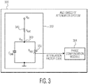
- Fig. 3 depicts an embodiment of the RF attenuator system depicted in Fig. 2 that is implemented as an AGC-based RF attenuator system 300.
- the AGC-based RF attenuator system 300 is a programmable resistive voltage divider that includes a resistor 340 with a fixed external resistance, Rext, a tunable resistor 350 with a programmable resistance, Ragc, and a phase compensation module 304.
- the resistor 340 and the tunable resistor 350 form an AGC-based RF attenuator or a signal attenuation module 302.
- the RF attenuator system depicted in Fig. 2 is not limited to the embodiment shown in Fig. 3 .
- the resistor 340 may have a programmable resistance.
- a device with a programmable impedance may be used instead of the resistor.
- the AGC-based RF attenuator system 300 is used to attenuate an input signal into an output signal with lower amplitude (e.g., to provide a constant output signal amplitude or a relatively constant output signal amplitude within a threshold (e.g., within ⁇ 10%, 20% or other percentage of a predetermined output signal amplitude).
- the AGC-based RF attenuator system can be used to attenuate an input voltage to generate a reference level and/or to regulate the input voltage to have a lower dynamic range.
- the AGC-based attenuator system may have a non-constant or nonlinear phase response depending on the components and the settings of the AGC-based attenuator 302. For example, different resistance values of the resistors 340 or 350 can affect the phase behavior of the AGC-based attenuator system.
- the AGC-based RF attenuator system 300 attenuates an input voltage, "Vin,” into an attenuated voltage, "Vrx,” by voltage division.
- a capacitance Cpar which may be, for example, the chip pin capacitance or the substrate parasitic capacitance, is the capacitance coupled between the tunable resistor 350 and the attenuated voltage, Vrx.
- the division ratio can be adjusted by controlling the resistance value of the tunable resistor 350.
- the resistor 340 is connected to the input terminal from which the input voltage, Vin, is received and the tunable resistor 350 is connected to ground.
- the tunable resistor 350 may be connected to the input terminal from which the input voltage, Vin, is received and the resistor 340 is connected to ground.
- the voltage division ratio of the AGC-based RF attenuator system is adjusted by changing the resistance of the tunable resistor 350.
- the resistance, Ragc, of the tunable resistor, 350 is controlled by an attenuation factor code.
- the tunable resistor 350 may include a number of resistors and each of the resistors can be enabled or disabled (e.g., bypassed) by the attenuation factor code to generate a particular resistance value.
- the phase compensation module 304 maps the attenuation factor code of the AGC-based RF attenuator system 300 to a phase compensation value using a table (e.g., a look-up table (LUT)), a function, or a combination of a table and a function.
- a table e.g., a look-up table (LUT)
- the phase compensation module 304 determines the phase compensation value from a predetermined table of different phase compensation values and attenuation factor codes of the AGC-based RF attenuator system 300.
- Table 1A provides an example of a mapping between the attenuation factor code of the AGC-based RF attenuator system and the phase compensation value as a LUT while Table 1B provides some example values. Attenuation factor code values provided in the Table 1A and Table 1B can be approximated, rounded, or interpolated.
- the resistance value, Ragc, of the tunable resistor 350 is monotonic with respect to the attenuation factor code.
- the resistance value, Ragc, of the tunable resistor 350 may be linear or nonlinear with respect to the attenuation factor code.
- the phase compensation module can compensate for the phase response of the AGC-based RF attenuator system using various techniques.
- the phase compensation unit adjusts a DPLL setting of the AGC-based RF attenuator system according to the phase compensation value to maintain a constant phase response of the AGC-based RF attenuator system.
- the phase compensation unit adjusts a clock management setting of the AGC-based RF attenuator system according to the phase compensation value to maintain a constant phase response of the AGC-based RF attenuator system.
- the phase compensation unit implements or adjusts a delay element according to the phase compensation value to maintain a constant phase response of the AGC-based RF attenuator system. For example, for a phase compensation value of 27 degree, the phase compensation unit sets a delay element that is connected in serial with the AGC-based RF attenuator 302 with a first delay duration. For a phase compensation value of 10 degrees, the phase compensation unit sets the delay element with a second delay duration, which is smaller than the first delay duration.
- Table 1A Attenuation Factor Code Resistance (ohms) Phase Compensation (Degree) AGC_0 R_0 Phase_0 AGC_1 R_1 Phase_1 AGC_2 R_2 Phase_2 AGC_3 R_3 Phase_3 AGC_4 R_4 Phase_4 ... ... ... AGC_N R_N Phase_N Table 1B Attenuation Factor Code Resistance (ohms) Phase Compensation (Degree) 0 100,00 27 50 5,000 23 100 2,000 17 150 1,000 12 200 500 10 ... ... ... 1023 40 0
- the phase compensation module 304 determines the phase compensation value for the AGC-based RF attenuator system 300 based on a function of the attenuation factor code of the AGC-based RF attenuator 302.
- the phase of the transfer function of the AGC-based RF attenuator 302 under different attenuation factor codes can be obtained and the difference between the phase of the transfer function of the AGC-based RF attenuator 302 under different attenuation factor codes can be calculated by the phase compensation module.
- the phase compensation module can adjust a DPLL setting or a clock management setting of the AGC-based RF attenuator system 300 and/or implement or adjust a delay element to compensate for the phase difference of the transfer function of the AGC-based RF attenuator 302 under different attenuation factor codes. Consequently, a constant phase response of the AGC-based RF attenuator system 300 can be maintained.
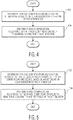
- Fig. 4 is a process flow diagram of a method for attenuator phase compensation in accordance with an embodiment of the invention.
- a phase compensation value for an attenuator is determined based on an attenuation configuration of the attenuator.
- phase compensation is performed according to the phase compensation value to maintain a constant phase response.
- the attenuator may be the same or similar to the attenuator 102 depicted in Fig. 1 and/or the AGC-based RF attenuator 302 depicted in Fig. 3 .
- Fig. 5 is a process flow diagram of a method for attenuator phase compensation in a communications device that communicates via inductive coupling in accordance with another embodiment of the invention.
- a phase compensation value for an attenuator that is located in a receiver path of the communications device is determined based on an attenuation configuration of the attenuator.
- phase compensation is performed according to the phase compensation value to maintain a constant phase response of the attenuator.
- the attenuator may be the same or similar to the attenuator 102 depicted in Fig. 1 and/or the AGC-based RF attenuator 302 depicted in Fig. 3 .
- the communications device may be the same or similar to the communications device 220 depicted in Fig. 2 .
- an embodiment of a computer program product includes a computer useable storage medium to store a computer readable program that, when executed on a computer, causes the computer to perform operations, as described herein.
- the computer-useable or computer-readable medium can be an electronic, magnetic, optical, electromagnetic, infrared, or semiconductor system (or apparatus or device), or a propagation medium.
- Examples of a computer-readable medium include a semiconductor or solid-state memory, magnetic tape, a removable computer diskette, a random access memory (RAM), a read-only memory (ROM), a rigid magnetic disc, and an optical disc.
- Current examples of optical discs include a compact disc with read only memory (CD-ROM), a compact disc with read/write (CD-R/W), a digital video disc (DVD), and a Blu-ray disc.
Landscapes
- Transmitters (AREA)
- Attenuators (AREA)
- Input Circuits Of Receivers And Coupling Of Receivers And Audio Equipment (AREA)
- Networks Using Active Elements (AREA)
Description
- Attenuators can be used to reduce the amplitude of electronic signals. For example, a Radio frequency (RF) attenuator is used to reduce the amplitude of an RF signal. However, the settings of an attenuator can affect the phase response of the attenuator, which can negatively affect the performance of a corresponding communications device. For example, under certain attenuation settings, an Automatic gain control (AGC)-based RF attenuator can exhibit a non-constant phase response.
- Embodiments of methods and systems for attenuator phase compensation are described. In an embodiment, a method for attenuator phase compensation involves determining a phase compensation value for an attenuator based on an attenuation configuration of the attenuator and performing phase compensation according to the phase compensation value to maintain a constant phase response.
- In an embodiment, determining the phase compensation value for the attenuator involves determining the phase compensation value for the attenuator from a predetermined table of different phase compensation values and attenuation configurations of the attenuator.
- In an embodiment, determining the phase compensation value for the attenuator involves determining the phase compensation value for the attenuator based on a function of the attenuation configuration of the attenuator.
- In an embodiment, the attenuation configuration of the attenuator includes an adjustable impedance value of the attenuator.
- In an embodiment, determining the phase compensation value for the attenuator involves determining the phase compensation value for the attenuator from a predetermined table of different phase compensation values and adjustable impedance configurations of the attenuator based on the adjustable impedance value of the attenuator.
- In an embodiment, the attenuation configuration of the attenuator includes an attenuation factor code of the attenuator.
- In an embodiment, determining the phase compensation value for the attenuator involves determining the phase compensation value for the attenuator from a predetermined table of different phase compensation values and attenuation factor codes of the attenuator.
- In an embodiment, determining the phase compensation value for the attenuator involves determining the phase compensation value for the attenuator based on a function of the attenuation factor code of the attenuator.
- In an embodiment, a system for attenuator phase compensation includes a phase compensation determination unit configured to determine a phase compensation value for an attenuator based on an attenuation configuration of the attenuator and a phase compensation unit configured to perform phase compensation according to the phase compensation value to maintain a constant phase response.
- In an embodiment, the phase compensation determination unit is further configured to determine the phase compensation value for the attenuator from a predetermined table of different phase compensation values and attenuation configurations of the attenuator.
- In an embodiment, the phase compensation determination unit is further configured to determine the phase compensation value for the attenuator based on a function of the attenuation configuration of the attenuator.
- In an embodiment, the attenuation configuration of the attenuator includes an adjustable impedance value of the attenuator.
- In an embodiment, the phase compensation determination unit is further configured to determine the phase compensation value for the attenuator from a predetermined table of different phase compensation values and adjustable impedance configurations of the attenuator based on the adjustable impedance value of the attenuator.
- In an embodiment, the attenuation configuration of the attenuator includes an attenuation factor code of the attenuator.
- In an embodiment, the phase compensation determination unit is further configured to determine the phase compensation value for the attenuator from a predetermined table of different phase compensation values and attenuation factor codes of the attenuator.
- In an embodiment, the phase compensation determination unit is further configured to determine the phase compensation value for the attenuator based on a function of the attenuation factor code of the attenuator.
- In an embodiment, a method for attenuator phase compensation in a communications device that communicates via inductive coupling involves determining a phase compensation value for an attenuator that is located in a receiver path of the communications device based on an attenuation configuration of the attenuator and performing phase compensation according to the phase compensation value to maintain a constant phase response of the attenuator.
- In an embodiment, determining the phase compensation value for the attenuator involves determining the phase compensation value for the attenuator from a predetermined table of different phase compensation values and attenuation configurations of the attenuator.
- In an embodiment, determining the phase compensation value for the attenuator involves determining the phase compensation value for the attenuator based on a function of the attenuation configuration of the attenuator.
- In an embodiment, the attenuation configuration of the attenuator includes an attenuation factor code of the attenuator.
- Other aspects and advantages of embodiments of the present invention will become apparent from the following detailed description taken in conjunction with the accompanying drawings.
-
-
Fig. 1 is a functional block diagram of an attenuator system in accordance with an embodiment of the invention. -
Fig. 2 depicts an embodiment of a communications device that can be used with a corresponding reader to form a communications system. -
Fig. 3 depicts an embodiment of the RF attenuator system depicted inFig. 2 that is implemented as an AGC-based RF attenuator. -
Fig. 4 is a process flow diagram of a method for attenuator phase compensation in accordance with an embodiment of the invention. -
Fig. 5 is a process flow diagram of a method for AGC-based attenuator phase compensation in accordance with an embodiment of the invention. - Throughout the description, similar reference numbers may be used to identify similar elements.
- It will be readily understood that the components of the embodiments as generally described herein and illustrated in the appended figures could be arranged and designed in a wide variety of different configurations. Thus, the following more detailed description of various embodiments, as represented in the figures, is not intended to limit the scope of the present disclosure, but is merely representative of various embodiments. While the various aspects of the embodiments are presented in drawings, the drawings are not necessarily drawn to scale unless specifically indicated.
- The present invention may be embodied in other specific forms without departing from its spirit or essential characteristics. The described embodiments are to be considered in all respects only as illustrative and not restrictive. The scope of the invention is, therefore, indicated by the appended claims rather than by this detailed description. All changes which come within the meaning and range of equivalency of the claims are to be embraced within their scope.
- Reference throughout this specification to features, advantages, or similar language does not imply that all of the features and advantages that may be realized with the present invention should be or are in any single embodiment of the invention. Rather, language referring to the features and advantages is understood to mean that a specific feature, advantage, or characteristic described in connection with an embodiment is included in at least one embodiment of the present invention. Thus, discussions of the features and advantages, and similar language, throughout this specification may, but do not necessarily, refer to the same embodiment.
- Furthermore, the described features, advantages, and characteristics of the invention may be combined in any suitable manner in one or more embodiments. One skilled in the relevant art will recognize, in light of the description herein, that the invention can be practiced without one or more of the specific features or advantages of a particular embodiment. In other instances, additional features and advantages may be recognized in certain embodiments that may not be present in all embodiments of the invention.
- Reference throughout this specification to "one embodiment," "an embodiment," or similar language means that a particular feature, structure, or characteristic described in connection with the indicated embodiment is included in at least one embodiment of the present invention. Thus, the phrases "in one embodiment," "in an embodiment," and similar language throughout this specification may, but do not necessarily, all refer to the same embodiment.
-
Fig. 1 is a functional block diagram of an attenuator system withphase compensation 100 in accordance with an embodiment of the invention. In the embodiment depicted inFig. 1 , the attenuator system includes an attenuator or asignal attenuation module 102 and aphase compensation module 104. The attenuator system may be an integrated circuit (IC) device or part of an IC device that includes additional components. The attenuator and the phase compensation module may be located on the same IC chip or on separate IC chips. Although the illustrated attenuator system is shown with certain components and described with certain functionality herein, other embodiments of the attenuator system may include fewer or more components to implement the same, less, or more functionality. - In the embodiment depicted in
Fig. 1 , theattenuator 102 is configured to process an input signal to generate a processed signal. The attenuator perform a signal attenuation operation in which the input signal is attenuated to generate an attenuated signal with an amplitude that is lower than the amplitude of the input signal and/or a signal bypass operation in which the input signal is not attenuated. For example, the attenuator is an RF attenuator that is used to reduce the amplitude of an RF input signal. The attenuator can be implemented as a programmable resistive voltage divider and/or a programmable capacitive voltage divider. Other implementations of the attenuator are possible. - The settings of the
attenuator 102 can affect the phase response of the attenuator, which can negatively affect the performance of the attenuator system and a corresponding communications device that contains the attenuator system. For example, the attenuator may be located at a receiver (RX) path of a communications device. In this case, depending on an attenuator setting, the attenuator and thus the RX path of the communications device, may have a non-constant phase response. In the embodiment depicted inFig. 1 , thephase compensation module 104 is configured to perform phase compensation. For example, the phase compensation module can adjust at least one parameter associated with the attenuator system in order to maintain a constant phase response of the attenuator system. Examples of a parameter associated with the attenuator system include, without being limited to, a component of the attenuator system, a setting of the attenuator system, and a signal that is input into the attenuator system or output from the attenuator system. The phase response of the attenuator is the relationship between the phase of a signal that is input to the attenuator (input signal) and the phase of a signal that is output from the attenuator (output signal). The phase response of the attenuator can change when an attenuation configuration, e.g., the attenuation factor, of the attenuator is adjusted. In the embodiment depicted inFig. 1 , the phase compensation module obtains a phase offset/compensation value based on an attenuation configuration, e.g., the attenuation factor, of the attenuator. Consequently, a constant/linear phase response can be maintained in the attenuator system by compensating the phase response of the attenuator even if the amplitude of the input signal changes. By adjusting a parameter associated with the attenuator system, changes in the phase response of the attenuator can be compensated for to maintain a constant phase response of the attenuator system. Consequently, the performance of a corresponding communications device can be improved. - In some embodiments, the
phase compensation module 104 includes a phasecompensation determination unit 106 and aphase compensation unit 108. The phase compensation determination unit is configured to determine a phase compensation value based on an attenuation configuration of theattenuator 102. In an embodiment, the attenuation configuration of the attenuator is supplied to the phase compensation determination unit by the attenuator. Examples of the attenuation configuration include, without being limited to, the resistance value of the attenuator, the capacitance value of the attenuator and the attenuation factor code of the attenuator. The phase compensation determination unit may use the attenuation configuration of the attenuator as an index or a variable for a table (e.g., a lookup table) or a function to determine the phase compensation value. The phase compensation unit is configured to perform phase compensation of the phase response of the attenuator according to the phase compensation value to maintain a constant phase response of the attenuator. - The
phase compensation unit 108 can compensate for the phase response of theattenuator 102 using various techniques. In an embodiment, the phase compensation unit adjusts a digital phase-locked loop (DPLL) setting of the attenuator system according to the phase compensation value to maintain a constant phase response for theattenuator system 100. In another embodiment, the phase compensation unit adjusts a clock management setting of the attenuator system according to the phase compensation value to maintain a constant phase response for the attenuator system. In yet another embodiment, the phase compensation unit implements a delay element (e.g., a delay line in a clock path of the attenuator system) according to the phase compensation value to maintain a constant phase response for the attenuator system. -
Fig. 2 depicts an embodiment of acommunications device 220 that can be used with acorresponding reader 230 to form acommunications system 250. The corresponding reader may be a dedicated reader device or a communications device in reader-mode. In the embodiment depicted inFig. 2 , the communications device includes anRF attenuator system 200, amatching network 210 that is coupled to anantenna 212, an analog receiver "RX" 214, and an analog transmitter "TX" 218. The RF attenuator system and the analog receiver are located in a receiver path of the communications device while the analog transmitter is located in a transmitter path of the communications device. In some embodiments, the communications device is implemented in a handheld computing system or a mobile computing system, such as a mobile phone. The communications device may be a near field communications (NFC) device that utilizes inductive coupling to communicate. In some embodiments, the communications device is implemented as an RF transponder compatible with the International Organization for Standardization (ISO)/the International Electrotechnical Commission (IEC) 14443 standard. Although the illustrated communications device is shown with certain components and described with certain functionality herein, other embodiments of the communications device may include fewer or more components to implement the same, less, or more functionality. In addition, the RF attenuator system depicted inFig. 2 is one possible embodiment of theattenuator system 100 depicted inFig. 1 . However, the attenuator system depicted inFig. 1 is not limited to the embodiment shown inFig. 2 . - In some embodiments, the
communications system 250 is an inductively coupled communications system. In these embodiments, the antennas of thecommunications device 220 and the reader are induction type antennas such as loop antennas or coil-type antennas. In an example operation of the communications device, an RF signal is received by theantenna 212 via inductive coupling from theantenna 232 of the corresponding reader and is attenuated by theRF attenuator system 200. The attenuated RF signal is passed to theanalog receiver 214 to convert the attenuated RF signal into a digital signal. An outgoing RF signal is generated at theanalog transmitter 218, which is transmitted via inductive coupling using the antenna. In some embodiments, the communications device is an active load modulation (ALM) device. In such embodiments, the communications device can be configured to generate its own magnetic field for transmitting the outgoing RF using a current source, which results in greater communications distances. - The
RF attenuator system 200 is configured to perform a signal attenuation operation in which an RF signal is attenuated and/or a signal bypass operation in which an RF signal is not attenuated. In some embodiments, the RF attenuator system is used to attenuate an incoming RF signal automatically or under device/human control if the RF signal is larger than a supply range (e.g., to maintain a constant output signal amplitude) and to generate an attenuation factor code that has M bits (where M is a positive integer). The attenuation factor code can be used by other circuits. For example, the attenuation factor code may be used by a received signal strength indicator (RSSI) device to generate an RSSI value. In some embodiments, the RF attenuator system is implemented as an impedance divider, a programmable resistive voltage divider, a programmable capacitive voltage divider, or a combination of a programmable resistive voltage divider and a programmable capacitive voltage divider. - In an example operation of the
communications device 200, an RF signal is received by the antenna from anantenna 232 of thecorresponding reader 230 and is attenuated by the RF attenuator system. The attenuated RF signal is passed to theanalog receiver 214 to convert the attenuated RF signal into a digital signal. An outgoing RF signal is generated at theanalog transmitter 218, which is transmitted via theantenna 212 to the reader. -
Fig. 3 depicts an embodiment of the RF attenuator system depicted inFig. 2 that is implemented as an AGC-basedRF attenuator system 300. In the embodiment depicted inFig. 3 , the AGC-basedRF attenuator system 300 is a programmable resistive voltage divider that includes aresistor 340 with a fixed external resistance, Rext, atunable resistor 350 with a programmable resistance, Ragc, and aphase compensation module 304. Theresistor 340 and thetunable resistor 350 form an AGC-based RF attenuator or asignal attenuation module 302. The AGC-basedRF attenuator system 300 depicted inFig. 3 is one possible embodiment of theRF attenuator system 200 depicted inFig. 2 . However, the RF attenuator system depicted inFig. 2 is not limited to the embodiment shown inFig. 3 . For example, in some embodiments, theresistor 340 may have a programmable resistance. In other embodiment, instead of the resistor, a device with a programmable impedance may be used. - The AGC-based
RF attenuator system 300 is used to attenuate an input signal into an output signal with lower amplitude (e.g., to provide a constant output signal amplitude or a relatively constant output signal amplitude within a threshold (e.g., within ±10%, 20% or other percentage of a predetermined output signal amplitude). For example, the AGC-based RF attenuator system can be used to attenuate an input voltage to generate a reference level and/or to regulate the input voltage to have a lower dynamic range. However, the AGC-based attenuator system may have a non-constant or nonlinear phase response depending on the components and the settings of the AGC-basedattenuator 302. For example, different resistance values of theresistors - In the embodiment depicted in
Fig. 3 , the AGC-basedRF attenuator system 300 attenuates an input voltage, "Vin," into an attenuated voltage, "Vrx," by voltage division. A capacitance Cpar, which may be, for example, the chip pin capacitance or the substrate parasitic capacitance, is the capacitance coupled between thetunable resistor 350 and the attenuated voltage, Vrx. The division ratio can be adjusted by controlling the resistance value of thetunable resistor 350. In the AGC-based RF attenuator system depicted inFig. 3 , theresistor 340 is connected to the input terminal from which the input voltage, Vin, is received and thetunable resistor 350 is connected to ground. Alternatively, thetunable resistor 350 may be connected to the input terminal from which the input voltage, Vin, is received and theresistor 340 is connected to ground. The voltage division ratio of the AGC-based RF attenuator system is adjusted by changing the resistance of thetunable resistor 350. - In some embodiments, the resistance, Ragc, of the tunable resistor, 350, is controlled by an attenuation factor code. The
tunable resistor 350 may include a number of resistors and each of the resistors can be enabled or disabled (e.g., bypassed) by the attenuation factor code to generate a particular resistance value. In an embedment, thephase compensation module 304 maps the attenuation factor code of the AGC-basedRF attenuator system 300 to a phase compensation value using a table (e.g., a look-up table (LUT)), a function, or a combination of a table and a function. - In some embodiments, the
phase compensation module 304 determines the phase compensation value from a predetermined table of different phase compensation values and attenuation factor codes of the AGC-basedRF attenuator system 300. Table 1A provides an example of a mapping between the attenuation factor code of the AGC-based RF attenuator system and the phase compensation value as a LUT while Table 1B provides some example values. Attenuation factor code values provided in the Table 1A and Table 1B can be approximated, rounded, or interpolated. In an embodiment, the resistance value, Ragc, of thetunable resistor 350 is monotonic with respect to the attenuation factor code. The resistance value, Ragc, of thetunable resistor 350 may be linear or nonlinear with respect to the attenuation factor code. The phase compensation module can compensate for the phase response of the AGC-based RF attenuator system using various techniques. In an embodiment, the phase compensation unit adjusts a DPLL setting of the AGC-based RF attenuator system according to the phase compensation value to maintain a constant phase response of the AGC-based RF attenuator system. In another embodiment, the phase compensation unit adjusts a clock management setting of the AGC-based RF attenuator system according to the phase compensation value to maintain a constant phase response of the AGC-based RF attenuator system. In yet another embodiment, the phase compensation unit implements or adjusts a delay element according to the phase compensation value to maintain a constant phase response of the AGC-based RF attenuator system. For example, for a phase compensation value of 27 degree, the phase compensation unit sets a delay element that is connected in serial with the AGC-basedRF attenuator 302 with a first delay duration. For a phase compensation value of 10 degrees, the phase compensation unit sets the delay element with a second delay duration, which is smaller than the first delay duration.Table 1A Attenuation Factor Code Resistance (ohms) Phase Compensation (Degree) AGC_0 R_0 Phase_0 AGC_1 R_1 Phase_1 AGC_2 R_2 Phase_2 AGC_3 R_3 Phase_3 AGC_4 R_4 Phase_4 ... ... ... AGC_N R_N Phase_N Table 1B Attenuation Factor Code Resistance (ohms) Phase Compensation (Degree) 0 100,00 27 50 5,000 23 100 2,000 17 150 1,000 12 200 500 10 ... ... ... 1023 40 0 - In some embodiments, the
phase compensation module 304 determines the phase compensation value for the AGC-basedRF attenuator system 300 based on a function of the attenuation factor code of the AGC-basedRF attenuator 302. For example, the impedance at thenode 360, at which the voltage, Vrx, is output can be expressed as:
node 360, Ragc represents the resistance value of thetunable resistor 350, Cagc represents all capacitances from Vrx to ground, including e.g., the parasitic capacitance Cpar coupled between thetunable resistor 350 and the attenuated voltage, Vrx, and capacitances of switches within thetunable resistor 350. The transfer function of the AGC-basedRF attenuator 302 can be expressed as:
RF attenuator 302 and Rext represents the resistance value of theresistor 340. Hence, the phase of the transfer function of the AGC-basedRF attenuator 302 can be expressed as:
RF attenuator 302. Based on the above equation (3), the phase of the transfer function of the AGC-basedRF attenuator 302 under different attenuation factor codes can be obtained and the difference between the phase of the transfer function of the AGC-basedRF attenuator 302 under different attenuation factor codes can be calculated by the phase compensation module. The phase compensation module can adjust a DPLL setting or a clock management setting of the AGC-basedRF attenuator system 300 and/or implement or adjust a delay element to compensate for the phase difference of the transfer function of the AGC-basedRF attenuator 302 under different attenuation factor codes. Consequently, a constant phase response of the AGC-basedRF attenuator system 300 can be maintained. -
Fig. 4 is a process flow diagram of a method for attenuator phase compensation in accordance with an embodiment of the invention. Atblock 402, a phase compensation value for an attenuator is determined based on an attenuation configuration of the attenuator. Atblock 404, phase compensation is performed according to the phase compensation value to maintain a constant phase response. The attenuator may be the same or similar to theattenuator 102 depicted inFig. 1 and/or the AGC-basedRF attenuator 302 depicted inFig. 3 . -
Fig. 5 is a process flow diagram of a method for attenuator phase compensation in a communications device that communicates via inductive coupling in accordance with another embodiment of the invention. Atblock 502, a phase compensation value for an attenuator that is located in a receiver path of the communications device is determined based on an attenuation configuration of the attenuator. Atblock 504, phase compensation is performed according to the phase compensation value to maintain a constant phase response of the attenuator. The attenuator may be the same or similar to theattenuator 102 depicted inFig. 1 and/or the AGC-basedRF attenuator 302 depicted inFig. 3 . The communications device may be the same or similar to thecommunications device 220 depicted inFig. 2 . - Although the operations of the method(s) herein are shown and described in a particular order, the order of the operations of each method may be altered so that certain operations may be performed in an inverse order or so that certain operations may be performed, at least in part, concurrently with other operations. In another embodiment, instructions or sub-operations of distinct operations may be implemented in an intermittent and/or alternating manner.
- It should also be noted that at least some of the operations for the methods may be implemented using software instructions stored on a computer useable storage medium for execution by a computer. As an example, an embodiment of a computer program product includes a computer useable storage medium to store a computer readable program that, when executed on a computer, causes the computer to perform operations, as described herein.
- The computer-useable or computer-readable medium can be an electronic, magnetic, optical, electromagnetic, infrared, or semiconductor system (or apparatus or device), or a propagation medium. Examples of a computer-readable medium include a semiconductor or solid-state memory, magnetic tape, a removable computer diskette, a random access memory (RAM), a read-only memory (ROM), a rigid magnetic disc, and an optical disc. Current examples of optical discs include a compact disc with read only memory (CD-ROM), a compact disc with read/write (CD-R/W), a digital video disc (DVD), and a Blu-ray disc.
- In the above description, specific details of various embodiments are provided. However, some embodiments may be practiced with less than all of these specific details. In other instances, certain methods, procedures, components, structures, and/or functions are described in no more detail than to enable the various embodiments of the invention, for the sake of brevity and clarity.
- Although specific embodiments of the invention have been described and illustrated, the invention is not to be limited to the specific forms or arrangements of parts so described and illustrated. The scope of the invention is to be defined by the claims appended hereto and their equivalents.
Claims (15)
- A method for attenuator phase compensation, the method comprising:determining a phase compensation value for an attenuator based on an attenuation configuration of the attenuator; andperforming phase compensation according to the phase compensation value to maintain a constant phase response.
- The method of claim 1, wherein determining the phase compensation value for the attenuator comprises determining the phase compensation value for the attenuator from a predetermined table of different phase compensation values and attenuation configurations of the attenuator.
- The method of claim 1 or 2, wherein determining the phase compensation value for the attenuator comprises determining the phase compensation value for the attenuator based on a function of the attenuation configuration of the attenuator.
- The method of any preceding claim, wherein the attenuation configuration of the attenuator comprises an adjustable impedance value of the attenuator.
- The method of claim 4, wherein determining the phase compensation value for the attenuator comprises determining the phase compensation value for the attenuator from a predetermined table of different phase compensation values and adjustable impedance configurations of the attenuator based on the adjustable impedance value of the attenuator.
- The method of any preceding claim, wherein the attenuation configuration of the attenuator comprises an attenuation factor code of the attenuator.
- The method of claim 6, wherein determining the phase compensation value for the attenuator comprises determining the phase compensation value for the attenuator from a predetermined table of different phase compensation values and attenuation factor codes of the attenuator.
- The method of claim 6, wherein determining the phase compensation value for the attenuator comprises determining the phase compensation value for the attenuator based on a function of the attenuation factor code of the attenuator.
- A system for attenuator phase compensation, the system comprising:a phase compensation determination unit configured to determine a phase compensation value for an attenuator based on an attenuation configuration of the attenuator; anda phase compensation unit configured to perform phase compensation according to the phase compensation value to maintain a constant phase response.
- The system of claim 9, wherein the phase compensation determination unit is further configured to determine the phase compensation value for the attenuator from a predetermined table of different phase compensation values and attenuation configurations of the attenuator.
- The system of claim 9 or 10, wherein the phase compensation determination unit is further configured to determine the phase compensation value for the attenuator based on a function of the attenuation configuration of the attenuator.
- The system of any one of claims 9 to 11, wherein the attenuation configuration of the attenuator comprises an adjustable impedance value of the attenuator.
- The system of claim 12, wherein the phase compensation determination unit is further configured to determine the phase compensation value for the attenuator from a predetermined table of different phase compensation values and adjustable impedance configurations of the attenuator based on the adjustable impedance value of the attenuator.
- The system of any one of claims 9 to 13, wherein the attenuation configuration of the attenuator comprises an attenuation factor code of the attenuator.
- The method of any one of claims 1 to 8, the method being applied in a communications device that communicates via inductive coupling, wherein the attenuator is located in a receiver path of the communications device.
Applications Claiming Priority (1)
| Application Number | Priority Date | Filing Date | Title |
|---|---|---|---|
| US15/224,933 US10659009B2 (en) | 2016-08-01 | 2016-08-01 | Method and system for attenuator phase compensation |
Publications (2)
| Publication Number | Publication Date |
|---|---|
| EP3280049A1 true EP3280049A1 (en) | 2018-02-07 |
| EP3280049B1 EP3280049B1 (en) | 2021-02-24 |
Family
ID=59520723
Family Applications (1)
| Application Number | Title | Priority Date | Filing Date |
|---|---|---|---|
| EP17182573.0A Active EP3280049B1 (en) | 2016-08-01 | 2017-07-21 | Method and system for attenuator phase compensation |
Country Status (4)
| Country | Link |
|---|---|
| US (1) | US10659009B2 (en) |
| EP (1) | EP3280049B1 (en) |
| JP (1) | JP2018023099A (en) |
| CN (1) | CN107681988B (en) |
Families Citing this family (4)
| Publication number | Priority date | Publication date | Assignee | Title |
|---|---|---|---|---|
| CN113114151B (en) * | 2021-04-29 | 2022-12-20 | 成都天锐星通科技有限公司 | Bandwidth reconfigurable radio frequency attenuator and phased array system |
| EP4109771B1 (en) | 2021-06-21 | 2026-01-28 | Nxp B.V. | Determining initial transmission phase offset in an nfc device |
| CN116032249B (en) * | 2022-12-12 | 2026-05-08 | 创远信科(上海)技术股份有限公司 | Methods, systems, processors, and computer-readable storage media for controlling digitally controlled attenuators in signal source power calibration. |
| CN121051347B (en) * | 2025-11-04 | 2026-02-17 | 杭州谱育科技发展有限公司 | Error compensation method for ICP-OES attenuators |
Citations (4)
| Publication number | Priority date | Publication date | Assignee | Title |
|---|---|---|---|---|
| JPH08162886A (en) * | 1994-12-07 | 1996-06-21 | Kokusai Electric Co Ltd | High frequency variable electronic attenuator with phase compensation |
| US20090237218A1 (en) * | 2007-06-08 | 2009-09-24 | Nam Yun Kim | Wireless communication device |
| US20160094187A1 (en) * | 2014-09-29 | 2016-03-31 | Freescale Semiconductor, Inc. | Modifiable signal adjustment devices for power amplifiers and corresponding methods & apparatus |
| US20160134259A1 (en) * | 2014-11-11 | 2016-05-12 | Peregrine Semiconductor Corporation | Digital Step Attenuator with Reduced Relative Phase Error |
Family Cites Families (19)
| Publication number | Priority date | Publication date | Assignee | Title |
|---|---|---|---|---|
| JP2891274B2 (en) * | 1992-10-05 | 1999-05-17 | 富士通株式会社 | Variable signal attenuator |
| US5918166A (en) * | 1994-11-30 | 1999-06-29 | Nec Corportion | Level control circuit for portable radio communication apparatus |
| JPH11340771A (en) * | 1998-05-27 | 1999-12-10 | Nec Eng Ltd | Attenuator and step attenuator |
| JP3642040B2 (en) * | 2001-05-31 | 2005-04-27 | 日本電気株式会社 | Distortion compensation circuit and distortion compensation method |
| US7212584B2 (en) * | 2002-08-05 | 2007-05-01 | Hitachi Kokusai Electric Inc. | Distortion compensator |
| JP4063628B2 (en) * | 2002-10-03 | 2008-03-19 | 株式会社日立国際電気 | Distortion compensation device |
| JP4313170B2 (en) * | 2003-12-08 | 2009-08-12 | マスプロ電工株式会社 | Signal amplification circuit, transmission antenna, and output level control method thereof |
| WO2004095709A2 (en) * | 2003-04-24 | 2004-11-04 | Koninklijke Philips Electronics N.V. | Gain compensation |
| FR2887094B1 (en) * | 2005-06-09 | 2008-02-01 | Airbus France Sas | METHOD AND DEVICE FOR INTERCEPTING TRANSITANT DATA ON A LINK OF AN ETHERNET NETWORK |
| JP4506719B2 (en) * | 2006-05-11 | 2010-07-21 | 日本電気株式会社 | Variable attenuation circuit for high frequency |
| US8849230B2 (en) * | 2011-03-03 | 2014-09-30 | Sony Corporation | Attenuator and method for attenuating |
| US9384373B2 (en) * | 2011-10-26 | 2016-07-05 | Qualcomm Incorporated | Adaptive signal scaling in NFC transceivers |
| US9203348B2 (en) * | 2012-01-27 | 2015-12-01 | Freescale Semiconductor, Inc. | Adjustable power splitters and corresponding methods and apparatus |
| JP2014241554A (en) * | 2013-06-12 | 2014-12-25 | 旭化成エレクトロニクス株式会社 | Attenuator |
| FR3010817B1 (en) | 2013-09-13 | 2016-12-23 | Inside Secure | METHOD AND DEVICE FOR DATA TRANSMISSION BY CONTROLLED AUTO-OSCILLATION INDUCTIVE COUPLING |
| US10224891B2 (en) * | 2013-12-12 | 2019-03-05 | Qorvo Us, Inc. | Radio frequency power amplifier with noise reduction feedback linearization |
| US10019608B2 (en) | 2015-12-09 | 2018-07-10 | Nxp B.V. | Method and device for phase calibration with active load modulation |
| US9853752B2 (en) | 2016-03-31 | 2017-12-26 | Nxp B.V. | Method and system for generating a received signal strength indicator (RSSI) value that corresponds to a radio frequency (RF) signal |
| US10756881B2 (en) | 2016-08-01 | 2020-08-25 | Nxp B.V. | Method and system for operating a communications device that communicates via inductive coupling |
-
2016
- 2016-08-01 US US15/224,933 patent/US10659009B2/en active Active
-
2017
- 2017-07-11 JP JP2017135606A patent/JP2018023099A/en active Pending
- 2017-07-21 EP EP17182573.0A patent/EP3280049B1/en active Active
- 2017-07-28 CN CN201710637285.3A patent/CN107681988B/en active Active
Patent Citations (4)
| Publication number | Priority date | Publication date | Assignee | Title |
|---|---|---|---|---|
| JPH08162886A (en) * | 1994-12-07 | 1996-06-21 | Kokusai Electric Co Ltd | High frequency variable electronic attenuator with phase compensation |
| US20090237218A1 (en) * | 2007-06-08 | 2009-09-24 | Nam Yun Kim | Wireless communication device |
| US20160094187A1 (en) * | 2014-09-29 | 2016-03-31 | Freescale Semiconductor, Inc. | Modifiable signal adjustment devices for power amplifiers and corresponding methods & apparatus |
| US20160134259A1 (en) * | 2014-11-11 | 2016-05-12 | Peregrine Semiconductor Corporation | Digital Step Attenuator with Reduced Relative Phase Error |
Also Published As
| Publication number | Publication date |
|---|---|
| CN107681988B (en) | 2023-09-29 |
| EP3280049B1 (en) | 2021-02-24 |
| CN107681988A (en) | 2018-02-09 |
| US10659009B2 (en) | 2020-05-19 |
| JP2018023099A (en) | 2018-02-08 |
| US20180034444A1 (en) | 2018-02-01 |
Similar Documents
| Publication | Publication Date | Title |
|---|---|---|
| US8760222B2 (en) | Method and apparatus for controlling or managing bandwidth of a filter circuit within a system having two integrated circuits | |
| US9806771B1 (en) | Method and system for high resolution tuning of the phase for active load modulation in a NFC system | |
| EP3280049B1 (en) | Method and system for attenuator phase compensation | |
| US10567092B2 (en) | System to calibrate phase using system information | |
| US9748912B2 (en) | Method and apparatus for detecting power | |
| CN107017897B (en) | Dynamic transmitter signal envelope shaping control for NFC or RFID devices | |
| US8903344B2 (en) | Programmable attenuator | |
| US9461716B2 (en) | Near field communications (NFC) modulation feedback apparatus for tuned antenna configurations | |
| US9154192B2 (en) | Method for controlling a modulation index of a near field communication device with aid of dynamic calibration, and associated apparatus | |
| US20110269416A1 (en) | Transmitter | |
| US10951190B2 (en) | On-chip harmonic filtering for radio frequency (RF) communications | |
| US9020455B1 (en) | Power control system for a receiver chain in a transceiver | |
| KR101621045B1 (en) | Adaptive signal scaling in nfc transceivers | |
| KR20180010883A (en) | Apparatus and method for matching antenna impedence in wireless communication system | |
| EP3319239B1 (en) | Method and system for automatic power control (apc) in a communications device that communicates via inductive coupling | |
| CN108206709B (en) | Method and system for operating a communication device communicating via inductive coupling | |
| US8903333B1 (en) | Adaptive antenna tuner for a transceiver | |
| WO2023019812A1 (en) | Compensation circuit module, power amplification assembly, compensation method, and device | |
| US6812789B2 (en) | RF power amplifier digital gain flattening over multiband frequencies | |
| JP2012019307A (en) | Receiver and transmitter receiver | |
| US9893751B2 (en) | Antenna circuit, communication device, and communication method for improving reception signal quality | |
| WO2013148225A1 (en) | Method and apparatus for compensating for phase shift in a communication device | |
| JP3112162B2 (en) | Transmission power control device and transmission power control method | |
| US10461811B2 (en) | Method and system for automatic power control (APC) in a communications device that communicates via inductive coupling | |
| CN110492910B (en) | NFC signal adjusting system and method |
Legal Events
| Date | Code | Title | Description |
|---|---|---|---|
| PUAI | Public reference made under article 153(3) epc to a published international application that has entered the european phase |
Free format text: ORIGINAL CODE: 0009012 |
|
| STAA | Information on the status of an ep patent application or granted ep patent |
Free format text: STATUS: THE APPLICATION HAS BEEN PUBLISHED |
|
| AK | Designated contracting states |
Kind code of ref document: A1 Designated state(s): AL AT BE BG CH CY CZ DE DK EE ES FI FR GB GR HR HU IE IS IT LI LT LU LV MC MK MT NL NO PL PT RO RS SE SI SK SM TR |
|
| AX | Request for extension of the european patent |
Extension state: BA ME |
|
| STAA | Information on the status of an ep patent application or granted ep patent |
Free format text: STATUS: REQUEST FOR EXAMINATION WAS MADE |
|
| 17P | Request for examination filed |
Effective date: 20180807 |
|
| RBV | Designated contracting states (corrected) |
Designated state(s): AL AT BE BG CH CY CZ DE DK EE ES FI FR GB GR HR HU IE IS IT LI LT LU LV MC MK MT NL NO PL PT RO RS SE SI SK SM TR |
|
| STAA | Information on the status of an ep patent application or granted ep patent |
Free format text: STATUS: EXAMINATION IS IN PROGRESS |
|
| 17Q | First examination report despatched |
Effective date: 20190212 |
|
| RIC1 | Information provided on ipc code assigned before grant |
Ipc: H03H 7/25 20060101AFI20200804BHEP Ipc: H03K 5/00 20060101ALN20200804BHEP |
|
| GRAP | Despatch of communication of intention to grant a patent |
Free format text: ORIGINAL CODE: EPIDOSNIGR1 |
|
| STAA | Information on the status of an ep patent application or granted ep patent |
Free format text: STATUS: GRANT OF PATENT IS INTENDED |
|
| INTG | Intention to grant announced |
Effective date: 20200911 |
|
| RIN1 | Information on inventor provided before grant (corrected) |
Inventor name: HUEBER, GERNOT Inventor name: MACNAMARA, IAN THOMAS |
|
| GRAJ | Information related to disapproval of communication of intention to grant by the applicant or resumption of examination proceedings by the epo deleted |
Free format text: ORIGINAL CODE: EPIDOSDIGR1 |
|
| STAA | Information on the status of an ep patent application or granted ep patent |
Free format text: STATUS: EXAMINATION IS IN PROGRESS |
|
| INTC | Intention to grant announced (deleted) | ||
| RIC1 | Information provided on ipc code assigned before grant |
Ipc: H03H 7/25 20060101AFI20201031BHEP Ipc: H03K 5/00 20060101ALN20201031BHEP |
|
| GRAP | Despatch of communication of intention to grant a patent |
Free format text: ORIGINAL CODE: EPIDOSNIGR1 |
|
| STAA | Information on the status of an ep patent application or granted ep patent |
Free format text: STATUS: GRANT OF PATENT IS INTENDED |
|
| RIC1 | Information provided on ipc code assigned before grant |
Ipc: H03H 7/25 20060101AFI20201118BHEP Ipc: H03K 5/00 20060101ALN20201118BHEP |
|
| INTG | Intention to grant announced |
Effective date: 20201216 |
|
| RAP1 | Party data changed (applicant data changed or rights of an application transferred) |
Owner name: NXP B.V. |
|
| GRAS | Grant fee paid |
Free format text: ORIGINAL CODE: EPIDOSNIGR3 |
|
| GRAA | (expected) grant |
Free format text: ORIGINAL CODE: 0009210 |
|
| STAA | Information on the status of an ep patent application or granted ep patent |
Free format text: STATUS: THE PATENT HAS BEEN GRANTED |
|
| AK | Designated contracting states |
Kind code of ref document: B1 Designated state(s): AL AT BE BG CH CY CZ DE DK EE ES FI FR GB GR HR HU IE IS IT LI LT LU LV MC MK MT NL NO PL PT RO RS SE SI SK SM TR |
|
| REG | Reference to a national code |
Ref country code: CH Ref legal event code: EP |
|
| REG | Reference to a national code |
Ref country code: DE Ref legal event code: R096 Ref document number: 602017033098 Country of ref document: DE |
|
| REG | Reference to a national code |
Ref country code: AT Ref legal event code: REF Ref document number: 1365766 Country of ref document: AT Kind code of ref document: T Effective date: 20210315 |
|
| REG | Reference to a national code |
Ref country code: IE Ref legal event code: FG4D |
|
| REG | Reference to a national code |
Ref country code: LT Ref legal event code: MG9D |
|
| REG | Reference to a national code |
Ref country code: NL Ref legal event code: MP Effective date: 20210224 |
|
| PG25 | Lapsed in a contracting state [announced via postgrant information from national office to epo] |
Ref country code: GR Free format text: LAPSE BECAUSE OF FAILURE TO SUBMIT A TRANSLATION OF THE DESCRIPTION OR TO PAY THE FEE WITHIN THE PRESCRIBED TIME-LIMIT Effective date: 20210525 Ref country code: HR Free format text: LAPSE BECAUSE OF FAILURE TO SUBMIT A TRANSLATION OF THE DESCRIPTION OR TO PAY THE FEE WITHIN THE PRESCRIBED TIME-LIMIT Effective date: 20210224 Ref country code: FI Free format text: LAPSE BECAUSE OF FAILURE TO SUBMIT A TRANSLATION OF THE DESCRIPTION OR TO PAY THE FEE WITHIN THE PRESCRIBED TIME-LIMIT Effective date: 20210224 Ref country code: NO Free format text: LAPSE BECAUSE OF FAILURE TO SUBMIT A TRANSLATION OF THE DESCRIPTION OR TO PAY THE FEE WITHIN THE PRESCRIBED TIME-LIMIT Effective date: 20210524 Ref country code: PT Free format text: LAPSE BECAUSE OF FAILURE TO SUBMIT A TRANSLATION OF THE DESCRIPTION OR TO PAY THE FEE WITHIN THE PRESCRIBED TIME-LIMIT Effective date: 20210624 Ref country code: BG Free format text: LAPSE BECAUSE OF FAILURE TO SUBMIT A TRANSLATION OF THE DESCRIPTION OR TO PAY THE FEE WITHIN THE PRESCRIBED TIME-LIMIT Effective date: 20210524 Ref country code: LT Free format text: LAPSE BECAUSE OF FAILURE TO SUBMIT A TRANSLATION OF THE DESCRIPTION OR TO PAY THE FEE WITHIN THE PRESCRIBED TIME-LIMIT Effective date: 20210224 |
|
| REG | Reference to a national code |
Ref country code: AT Ref legal event code: MK05 Ref document number: 1365766 Country of ref document: AT Kind code of ref document: T Effective date: 20210224 |
|
| PG25 | Lapsed in a contracting state [announced via postgrant information from national office to epo] |
Ref country code: NL Free format text: LAPSE BECAUSE OF FAILURE TO SUBMIT A TRANSLATION OF THE DESCRIPTION OR TO PAY THE FEE WITHIN THE PRESCRIBED TIME-LIMIT Effective date: 20210224 Ref country code: LV Free format text: LAPSE BECAUSE OF FAILURE TO SUBMIT A TRANSLATION OF THE DESCRIPTION OR TO PAY THE FEE WITHIN THE PRESCRIBED TIME-LIMIT Effective date: 20210224 Ref country code: RS Free format text: LAPSE BECAUSE OF FAILURE TO SUBMIT A TRANSLATION OF THE DESCRIPTION OR TO PAY THE FEE WITHIN THE PRESCRIBED TIME-LIMIT Effective date: 20210224 Ref country code: PL Free format text: LAPSE BECAUSE OF FAILURE TO SUBMIT A TRANSLATION OF THE DESCRIPTION OR TO PAY THE FEE WITHIN THE PRESCRIBED TIME-LIMIT Effective date: 20210224 Ref country code: SE Free format text: LAPSE BECAUSE OF FAILURE TO SUBMIT A TRANSLATION OF THE DESCRIPTION OR TO PAY THE FEE WITHIN THE PRESCRIBED TIME-LIMIT Effective date: 20210224 |
|
| PG25 | Lapsed in a contracting state [announced via postgrant information from national office to epo] |
Ref country code: IS Free format text: LAPSE BECAUSE OF FAILURE TO SUBMIT A TRANSLATION OF THE DESCRIPTION OR TO PAY THE FEE WITHIN THE PRESCRIBED TIME-LIMIT Effective date: 20210624 |
|
| PG25 | Lapsed in a contracting state [announced via postgrant information from national office to epo] |
Ref country code: SM Free format text: LAPSE BECAUSE OF FAILURE TO SUBMIT A TRANSLATION OF THE DESCRIPTION OR TO PAY THE FEE WITHIN THE PRESCRIBED TIME-LIMIT Effective date: 20210224 Ref country code: AT Free format text: LAPSE BECAUSE OF FAILURE TO SUBMIT A TRANSLATION OF THE DESCRIPTION OR TO PAY THE FEE WITHIN THE PRESCRIBED TIME-LIMIT Effective date: 20210224 Ref country code: EE Free format text: LAPSE BECAUSE OF FAILURE TO SUBMIT A TRANSLATION OF THE DESCRIPTION OR TO PAY THE FEE WITHIN THE PRESCRIBED TIME-LIMIT Effective date: 20210224 Ref country code: CZ Free format text: LAPSE BECAUSE OF FAILURE TO SUBMIT A TRANSLATION OF THE DESCRIPTION OR TO PAY THE FEE WITHIN THE PRESCRIBED TIME-LIMIT Effective date: 20210224 |
|
| REG | Reference to a national code |
Ref country code: DE Ref legal event code: R097 Ref document number: 602017033098 Country of ref document: DE |
|
| PG25 | Lapsed in a contracting state [announced via postgrant information from national office to epo] |
Ref country code: DK Free format text: LAPSE BECAUSE OF FAILURE TO SUBMIT A TRANSLATION OF THE DESCRIPTION OR TO PAY THE FEE WITHIN THE PRESCRIBED TIME-LIMIT Effective date: 20210224 Ref country code: RO Free format text: LAPSE BECAUSE OF FAILURE TO SUBMIT A TRANSLATION OF THE DESCRIPTION OR TO PAY THE FEE WITHIN THE PRESCRIBED TIME-LIMIT Effective date: 20210224 Ref country code: SK Free format text: LAPSE BECAUSE OF FAILURE TO SUBMIT A TRANSLATION OF THE DESCRIPTION OR TO PAY THE FEE WITHIN THE PRESCRIBED TIME-LIMIT Effective date: 20210224 |
|
| PLBE | No opposition filed within time limit |
Free format text: ORIGINAL CODE: 0009261 |
|
| STAA | Information on the status of an ep patent application or granted ep patent |
Free format text: STATUS: NO OPPOSITION FILED WITHIN TIME LIMIT |
|
| PG25 | Lapsed in a contracting state [announced via postgrant information from national office to epo] |
Ref country code: ES Free format text: LAPSE BECAUSE OF FAILURE TO SUBMIT A TRANSLATION OF THE DESCRIPTION OR TO PAY THE FEE WITHIN THE PRESCRIBED TIME-LIMIT Effective date: 20210224 Ref country code: AL Free format text: LAPSE BECAUSE OF FAILURE TO SUBMIT A TRANSLATION OF THE DESCRIPTION OR TO PAY THE FEE WITHIN THE PRESCRIBED TIME-LIMIT Effective date: 20210224 |
|
| 26N | No opposition filed |
Effective date: 20211125 |
|
| PG25 | Lapsed in a contracting state [announced via postgrant information from national office to epo] |
Ref country code: SI Free format text: LAPSE BECAUSE OF FAILURE TO SUBMIT A TRANSLATION OF THE DESCRIPTION OR TO PAY THE FEE WITHIN THE PRESCRIBED TIME-LIMIT Effective date: 20210224 |
|
| REG | Reference to a national code |
Ref country code: CH Ref legal event code: PL |
|
| GBPC | Gb: european patent ceased through non-payment of renewal fee |
Effective date: 20210721 |
|
| PG25 | Lapsed in a contracting state [announced via postgrant information from national office to epo] |
Ref country code: MC Free format text: LAPSE BECAUSE OF FAILURE TO SUBMIT A TRANSLATION OF THE DESCRIPTION OR TO PAY THE FEE WITHIN THE PRESCRIBED TIME-LIMIT Effective date: 20210224 |
|
| REG | Reference to a national code |
Ref country code: BE Ref legal event code: MM Effective date: 20210731 |
|
| PG25 | Lapsed in a contracting state [announced via postgrant information from national office to epo] |
Ref country code: LI Free format text: LAPSE BECAUSE OF NON-PAYMENT OF DUE FEES Effective date: 20210731 Ref country code: IT Free format text: LAPSE BECAUSE OF FAILURE TO SUBMIT A TRANSLATION OF THE DESCRIPTION OR TO PAY THE FEE WITHIN THE PRESCRIBED TIME-LIMIT Effective date: 20210224 Ref country code: GB Free format text: LAPSE BECAUSE OF NON-PAYMENT OF DUE FEES Effective date: 20210721 Ref country code: CH Free format text: LAPSE BECAUSE OF NON-PAYMENT OF DUE FEES Effective date: 20210731 |
|
| PG25 | Lapsed in a contracting state [announced via postgrant information from national office to epo] |
Ref country code: IS Free format text: LAPSE BECAUSE OF FAILURE TO SUBMIT A TRANSLATION OF THE DESCRIPTION OR TO PAY THE FEE WITHIN THE PRESCRIBED TIME-LIMIT Effective date: 20210624 Ref country code: LU Free format text: LAPSE BECAUSE OF NON-PAYMENT OF DUE FEES Effective date: 20210721 |
|
| PG25 | Lapsed in a contracting state [announced via postgrant information from national office to epo] |
Ref country code: IE Free format text: LAPSE BECAUSE OF NON-PAYMENT OF DUE FEES Effective date: 20210721 Ref country code: BE Free format text: LAPSE BECAUSE OF NON-PAYMENT OF DUE FEES Effective date: 20210731 |
|
| PG25 | Lapsed in a contracting state [announced via postgrant information from national office to epo] |
Ref country code: HU Free format text: LAPSE BECAUSE OF FAILURE TO SUBMIT A TRANSLATION OF THE DESCRIPTION OR TO PAY THE FEE WITHIN THE PRESCRIBED TIME-LIMIT; INVALID AB INITIO Effective date: 20170721 |
|
| PG25 | Lapsed in a contracting state [announced via postgrant information from national office to epo] |
Ref country code: CY Free format text: LAPSE BECAUSE OF FAILURE TO SUBMIT A TRANSLATION OF THE DESCRIPTION OR TO PAY THE FEE WITHIN THE PRESCRIBED TIME-LIMIT Effective date: 20210224 |
|
| P01 | Opt-out of the competence of the unified patent court (upc) registered |
Effective date: 20230725 |
|
| PG25 | Lapsed in a contracting state [announced via postgrant information from national office to epo] |
Ref country code: MK Free format text: LAPSE BECAUSE OF FAILURE TO SUBMIT A TRANSLATION OF THE DESCRIPTION OR TO PAY THE FEE WITHIN THE PRESCRIBED TIME-LIMIT Effective date: 20210224 |
|
| PG25 | Lapsed in a contracting state [announced via postgrant information from national office to epo] |
Ref country code: TR Free format text: LAPSE BECAUSE OF FAILURE TO SUBMIT A TRANSLATION OF THE DESCRIPTION OR TO PAY THE FEE WITHIN THE PRESCRIBED TIME-LIMIT Effective date: 20210224 |
|
| PG25 | Lapsed in a contracting state [announced via postgrant information from national office to epo] |
Ref country code: MT Free format text: LAPSE BECAUSE OF FAILURE TO SUBMIT A TRANSLATION OF THE DESCRIPTION OR TO PAY THE FEE WITHIN THE PRESCRIBED TIME-LIMIT Effective date: 20210224 |
|
| PGFP | Annual fee paid to national office [announced via postgrant information from national office to epo] |
Ref country code: FR Payment date: 20250620 Year of fee payment: 9 |
|
| PGFP | Annual fee paid to national office [announced via postgrant information from national office to epo] |
Ref country code: DE Payment date: 20250620 Year of fee payment: 9 |