EP3278718A1 - Imaging device - Google Patents
Imaging device Download PDFInfo
- Publication number
- EP3278718A1 EP3278718A1 EP16834830.8A EP16834830A EP3278718A1 EP 3278718 A1 EP3278718 A1 EP 3278718A1 EP 16834830 A EP16834830 A EP 16834830A EP 3278718 A1 EP3278718 A1 EP 3278718A1
- Authority
- EP
- European Patent Office
- Prior art keywords
- clock
- video signal
- memory
- processor
- sensor
- Prior art date
- Legal status (The legal status is an assumption and is not a legal conclusion. Google has not performed a legal analysis and makes no representation as to the accuracy of the status listed.)
- Withdrawn
Links
- 238000003384 imaging method Methods 0.000 title claims abstract description 71
- 230000001360 synchronised effect Effects 0.000 claims abstract description 31
- 238000006243 chemical reaction Methods 0.000 claims description 3
- 238000011084 recovery Methods 0.000 claims description 2
- 230000004048 modification Effects 0.000 description 42
- 238000012986 modification Methods 0.000 description 42
- 238000003780 insertion Methods 0.000 description 13
- 230000037431 insertion Effects 0.000 description 13
- 238000012545 processing Methods 0.000 description 11
- 238000012546 transfer Methods 0.000 description 10
- 230000005540 biological transmission Effects 0.000 description 8
- 238000000034 method Methods 0.000 description 7
- 230000006870 function Effects 0.000 description 5
- 230000008859 change Effects 0.000 description 3
- 238000005286 illumination Methods 0.000 description 3
- 238000005452 bending Methods 0.000 description 2
- 230000008569 process Effects 0.000 description 2
- 238000009825 accumulation Methods 0.000 description 1
- 238000012937 correction Methods 0.000 description 1
- 230000002596 correlated effect Effects 0.000 description 1
- 239000004973 liquid crystal related substance Substances 0.000 description 1
- 230000004044 response Effects 0.000 description 1
- 238000005096 rolling process Methods 0.000 description 1
- 238000005070 sampling Methods 0.000 description 1
Images



Classifications
-
- A—HUMAN NECESSITIES
- A61—MEDICAL OR VETERINARY SCIENCE; HYGIENE
- A61B—DIAGNOSIS; SURGERY; IDENTIFICATION
- A61B1/00—Instruments for performing medical examinations of the interior of cavities or tubes of the body by visual or photographical inspection, e.g. endoscopes; Illuminating arrangements therefor
- A61B1/00002—Operational features of endoscopes
- A61B1/00004—Operational features of endoscopes characterised by electronic signal processing
- A61B1/00009—Operational features of endoscopes characterised by electronic signal processing of image signals during a use of endoscope
-
- A—HUMAN NECESSITIES
- A61—MEDICAL OR VETERINARY SCIENCE; HYGIENE
- A61B—DIAGNOSIS; SURGERY; IDENTIFICATION
- A61B1/00—Instruments for performing medical examinations of the interior of cavities or tubes of the body by visual or photographical inspection, e.g. endoscopes; Illuminating arrangements therefor
- A61B1/00002—Operational features of endoscopes
- A61B1/00004—Operational features of endoscopes characterised by electronic signal processing
- A61B1/00006—Operational features of endoscopes characterised by electronic signal processing of control signals
-
- A—HUMAN NECESSITIES
- A61—MEDICAL OR VETERINARY SCIENCE; HYGIENE
- A61B—DIAGNOSIS; SURGERY; IDENTIFICATION
- A61B1/00—Instruments for performing medical examinations of the interior of cavities or tubes of the body by visual or photographical inspection, e.g. endoscopes; Illuminating arrangements therefor
- A61B1/00002—Operational features of endoscopes
- A61B1/0002—Operational features of endoscopes provided with data storages
-
- A—HUMAN NECESSITIES
- A61—MEDICAL OR VETERINARY SCIENCE; HYGIENE
- A61B—DIAGNOSIS; SURGERY; IDENTIFICATION
- A61B1/00—Instruments for performing medical examinations of the interior of cavities or tubes of the body by visual or photographical inspection, e.g. endoscopes; Illuminating arrangements therefor
- A61B1/00002—Operational features of endoscopes
- A61B1/00043—Operational features of endoscopes provided with output arrangements
- A61B1/00045—Display arrangement
- A61B1/0005—Display arrangement combining images e.g. side-by-side, superimposed or tiled
-
- A—HUMAN NECESSITIES
- A61—MEDICAL OR VETERINARY SCIENCE; HYGIENE
- A61B—DIAGNOSIS; SURGERY; IDENTIFICATION
- A61B1/00—Instruments for performing medical examinations of the interior of cavities or tubes of the body by visual or photographical inspection, e.g. endoscopes; Illuminating arrangements therefor
- A61B1/04—Instruments for performing medical examinations of the interior of cavities or tubes of the body by visual or photographical inspection, e.g. endoscopes; Illuminating arrangements therefor combined with photographic or television appliances
- A61B1/045—Control thereof
-
- G—PHYSICS
- G02—OPTICS
- G02B—OPTICAL ELEMENTS, SYSTEMS OR APPARATUS
- G02B23/00—Telescopes, e.g. binoculars; Periscopes; Instruments for viewing the inside of hollow bodies; Viewfinders; Optical aiming or sighting devices
- G02B23/24—Instruments or systems for viewing the inside of hollow bodies, e.g. fibrescopes
-
- H—ELECTRICITY
- H03—ELECTRONIC CIRCUITRY
- H03L—AUTOMATIC CONTROL, STARTING, SYNCHRONISATION OR STABILISATION OF GENERATORS OF ELECTRONIC OSCILLATIONS OR PULSES
- H03L7/00—Automatic control of frequency or phase; Synchronisation
- H03L7/06—Automatic control of frequency or phase; Synchronisation using a reference signal applied to a frequency- or phase-locked loop
- H03L7/08—Details of the phase-locked loop
- H03L7/0807—Details of the phase-locked loop concerning mainly a recovery circuit for the reference signal
-
- H—ELECTRICITY
- H04—ELECTRIC COMMUNICATION TECHNIQUE
- H04N—PICTORIAL COMMUNICATION, e.g. TELEVISION
- H04N25/00—Circuitry of solid-state image sensors [SSIS]; Control thereof
- H04N25/70—SSIS architectures; Circuits associated therewith
- H04N25/71—Charge-coupled device [CCD] sensors; Charge-transfer registers specially adapted for CCD sensors
-
- H—ELECTRICITY
- H04—ELECTRIC COMMUNICATION TECHNIQUE
- H04N—PICTORIAL COMMUNICATION, e.g. TELEVISION
- H04N25/00—Circuitry of solid-state image sensors [SSIS]; Control thereof
- H04N25/70—SSIS architectures; Circuits associated therewith
- H04N25/76—Addressed sensors, e.g. MOS or CMOS sensors
Definitions
- the present invention relates to an imaging apparatus.
- Jpn. Pat. Appln. KOKAI Publication No. 2013-000452 discloses the electronic endoscope apparatus configured to generate the display clock from the transmission clock transmitted from the scope distal end to the image processor and to perform display in accordance with the generated display clock.
- the electronic endoscope apparatus of Jpn. Pat. Appln. KOKAI Publication No. 2013-000452 is further configured to generate the imaging clock from the transmission clock transmitted from the image processor to the scope distal end and to perform imaging in accordance with the imaging clock generated.
- scopes that function as imaging apparatuses in the endoscope or the extracorporeal camera are configured to be replaceable with respect to the processor.
- the individual scopes often operate with clocks having different frequencies because of different performance, etc. of the imaging elements.
- the processor If the processor is configured to synchronize the imaging operation and the display operation by generating the display clock, the processor needs to have a circuit configuration capable of receiving clocks of various kinds of frequencies for every scope having differing demands. Therefore, it is easy for the configuration of the processor to become complicated. Also, with an increase in the operating speed because of the increased number of pixels of the imaging element, high quality of the drive clock of the imaging element has been demanded. In the configuration in which the imaging element is driven based on the clock from the processor, it is difficult to realize the imaging element that requires a clock of higher quality than the conventional one. It is also difficult to replace scopes.
- the present invention has been made in consideration of the circumstances described above, and an object is to provide an imaging apparatus with a simplified processor and capability for various scopes and capable of driving the imaging element by a clock of high quality.
- an imaging apparatus that includes an imaging element that outputs a video signal and to which a processor drive clock is input from an external image processor, the imaging apparatus comprises: a clock generation circuit that generates a clock synchronized with the video signal output from the imaging element; and a memory that stores the video signal output from the imaging element in synchronization with the clock synchronized with the video signal and outputs the stored video signal in synchronization with the processor drive clock.
- FIG. 1 schematically shows the structure of an endoscope system including an imaging apparatus according to one embodiment of the present invention.
- An endoscope system 1 of FIG. 1 includes a scope 10, a controller 20, and a monitor 30.
- the scope 10 transmits a video signal inside the subject body to an image processor 22 of the controller 20.
- the image processor 22 processes the video signal transmitted from the scope 10.
- the monitor 30 displays the video based on the video signal processed by the controller 20.
- the scope 10 that functions as the imaging apparatus in the present embodiment includes an insertion section 11, an operation unit 14, a cable 15, a connector 16, and a connector 17.
- the insertion section 11 is a section inserted into the subject body.
- An imaging element 12 is arranged inside the distal end of the insertion section 11.
- the imaging element 12 is a CMOS sensor or a CCD sensor and is configured to image an interior of the subject body in synchronization with the sensor drive clock to generate the video signal relating to the subject body.
- the insertion section 11 is further configured to emit illumination light from the distal end.
- the insertion section 11 includes a portion configured to bend in response to operation of an operation knob at the operation unit 14 performed by an operator such as a doctor, and a portion configured to bend passively by external force, not by operation of the operation unit 14.
- the operation unit 14 connects the insertion section 11 and the cable 15.
- the operation unit 14 includes an RL knob for bending the insertion section 11 rightward or leftward, and a UD knob for bending the insertion section 11 upward or downward.
- the operation unit 14 includes various switches.
- a light guide is arranged inside the insertion section 11, the operation unit 14, and the cable 15.
- the light guide is connected to a light source apparatus 21 of the controller 20 via the connector 16 provided at the proximal end of the cable 15.
- Various signal lines are arranged inside the insertion section 11, the operation unit 14, and the cable 15. The signal lines are connected to an image processor 22 of the controller 20 via the connector 17 that is connected to the connector 16.
- the light source apparatus 21 includes a light source such as a white LED, and emits illumination light.
- the illumination light emitted from the light source apparatus 21 is transmitted to the distal end of the insertion section 11 via the light guide and emitted from the distal end of the insertion section 11.
- the interior of the subject body is illuminated accordingly.
- the image processor 22 processes the video signal obtained by the imaging element 12 of the insertion section 11. This processing includes the processing of converting to a format where the video signal can be displayed on the monitor 30, e.g. , gradation correction processing, etc.
- the image processor 22 generates a processor drive clock and inputs the generated processor drive clock to the connector 17 and the monitor 30.
- the processor drive clock may or may not be synchronized with the sensor drive clock.
- the image processor 22 and the light source apparatus 21 are arranged independently in the controller 20, but they may be configured as a single housing.
- the monitor 30 is, for example, a liquid crystal monitor.
- the monitor 30 displays video and various kinds of information based on the video signal processed by the image processor 22, in synchronization with the processor drive clock generated by the image processor 22.
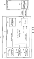
- FIG. 2 shows a main configuration of an endoscope system 1 according to the present embodiment.
- the imaging element 12 performs an imaging operation in accordance with the sensor drive clock that is independent of the processor drive clock generated by the image processor 22.
- the clock change is performed at the connector 17 to synchronize the imaging operation by the imaging element 12 and the display operation by the monitor 30.
- the clock change processing and the like are carried out at the connector 17, but a similar function may be provided at any other portions in the scope, e.g., the connector 16 or the operation unit 14.
- the first example is an example of the configuration in which the imaging element 12 is a CMOS sensor 121.
- the CMOS sensor 121 includes a sensor unit 122, a correlated double sampling (CDS) unit 123, and an A/D unit 124.
- CDS correlated double sampling
- the sensor unit 122 includes pixels arranged two dimensionally. Each pixel is formed, for example, by a photodiode, and outputs an analog electronic signal (video signal) in accordance with incident light.
- the CDS unit 123 performs processing of removing a reset noise component (dark current component) in the video signal output from the sensor unit 122.
- the A/D unit 124 converts the video signal, output sequentially from the CDS unit 123, to a digital signal.
- the sensor drive clock controls signal accumulation and signal readout of each pixel. For example, in the case where exposure of the CMOS sensor is controlled by a rolling shutter method, the exposure time of pixels at each row of the sensor unit 122 is controlled in accordance with the sensor drive clock.
- the connector 17 includes a sensor drive clock generation circuit 171 and the memory 172.
- the sensor drive clock generation circuit 171 is a circuit that generates a sensor drive clock necessary for driving the CMOS sensor 121.
- the sensor drive clock is generated by multiplying/dividing a basic clock having a predetermined frequency, for example.
- the memory 172 is a memory that temporarily stores a digital video signal output from the CMOS sensor 121.
- the memory 172 includes two clock input terminals, and is a memory in which the video signal is written using the clock synchronized with the video signal as a writing clock and from which the video signal is read out using the processor drive clock as a readout clock. Details of the "clock synchronized with the video signal" will be described later.
- Examples of the memory 172 include a line memory capable of storing a video signal for one row output from the A/D unit 124. This is because, in general, the video signal is output from the CMOS sensor 121 on a row-by-row basis.
- a frame memory such as SRAM can be used.
- the controls of writing to and reading from the memory may be performed by generating a writing address and reading address, or by using a memory that operates as FIFO.
- the image processor 22 includes a processor drive clock generation circuit 221.
- the processor drive clock generation circuit 221 is a circuit for generating a processor drive clock necessary for driving the image processor 22 and the monitor 30.
- the image processor 22 specifies a vertical position and a horizontal position of the video signal transmitted from the scope 10 and performs image processing in accordance with the processor drive clock.
- the processor drive clock is generated by multiplying/dividing a basic clock having a predetermined frequency, for example.
- the frequency of the basic clock for generating the processor drive clock and the frequency of the basic clock for generating the sensor drive clock may be the same or different.
- the scope 10, the light source apparatus 21 and the image processor 22 of the endoscope system 1 are powered on.
- the sensor drive clock generation circuit 171 of the scope 10 inputs the sensor drive clock to the imaging element 12 (CMOS sensor 121) .
- the CMOS sensor 121 controls exposure of each pixel row of the sensor unit 122 in accordance with the sensor drive clock.
- the video signal is output from the sensor unit 122 each time the exposure of each pixel row is ended.
- the reset noise of the video signal output from the sensor unit 122 is removed at the CDS unit 123.
- the video signal output from the CDS unit 123 is converted into a digital signal by the A/D unit 124, and is output.
- the video signal from the CMOS sensor 121 is serially transmitted, for example.
- the frequency of the transmission clock of the video signal can be different from the frequency of the sensor drive clock.
- the "clock synchronized with the video signal" is a clock in which the sensor drive clock is multiplied/divided. Specific examples of the clock synchronized with the video signal will be explained later.
- the memory 172 starts writing of the video signal output from the CMOS sensor 121 in synchronization with the start of the output of the video signal from the CMOS sensor 121. That is, the memory 172 stores the video signal to be output in a pixel row unit basis from the CMOS sensor 121 in accordance with the input of the clock synchronized with the video signal.
- the writing of the video signal in the memory 172 is performed in synchronization with the clock synchronized with the video signal. Because the clock synchronized with the video signal is in synchronization with the sensor drive clock, the imaging operation by the CMOS sensor 121 and the writing operation of the video signal to the memory 172 are synchronized.
- the processor drive clock generation circuit 221 of the image processor 22 inputs the processor drive clock to the memory 172.
- the memory 172 outputs the stored video signal in accordance with the input of the processor drive clock. Reading out the video signal from the memory 172 is performed in synchronization with the processor drive clock. That is, the clock synchronized with the video signal output from the memory 172 is changed to the processor drive clock.
- the image processor 22 specifies a vertical position and a horizontal position in the video signal in accordance with the processor drive clock and applies image processing to the video signal.
- the image processor 22 outputs the video signal subjected to the image processing to the monitor 30 in synchronization with the processor drive clock.
- the monitor 30 displays the video based on the video signal output from the image processor 22 in synchronization with the processor drive clock.
- the memory 172 is used to change the "clock synchronized with the video signal" to the processor drive clock.
- the imaging element 12 CMOS sensor 1211 uses the clock having a frequency different from that of the image processor 22, synchronization between the imaging operation and the display operation is maintained.
- the memory 172 is provided in the scope 10, not the image processor 22. Therefore, the configuration of the image processor 22 can be simplified.
- the image processor 22 does not have to include a receiving circuitry for receiving various types of video signals of different frequencies. From this aspect also, the configuration of the image processor 22 can be simplified.
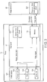
- FIG. 3 shows a main configuration of the endoscope system 1 according to Modification 1.
- Modification 1 is an example in which the sensor drive clock is used as the "clock synchronized with the video signal".
- the video signal output from the CMOS sensor 121 is output in accordance with the transmission clock of the same frequency as that of the sensor drive clock (the sensor drive clock itself may be used).
- the sensor drive clock generated by the sensor drive clock generation circuit 171 is input into the CMOS sensor 121 and also into the memory 172.
- the memory 172 stores the video signal from the CMOS sensor 121 in accordance with the input of the sensor drive clock and outputs the stored video signal to the image processor 22 in accordance with the input of the processor drive clock.
- the sensor drive clock generation circuit 171 is used as the clock generation circuit for generating the "clock synchronized with the video signal".
- FIG. 4 shows a main configuration of the endoscope system 1 according to Modification 2.
- FIG. 4 structures that are the same as those shown in FIG. 2 are specified by the same reference symbols as those in FIG. 2 , and explanations thereof are omitted.
- Modification 2 is an example in which a clock generated by multiplying the sensor drive clock is used as the "clock synchronized with the video signal".
- the sensor drive clock generated by the sensor drive clock generation circuit 171 is input into the CMOS sensor 121 and also into the frequency multiplication circuit 173.
- the frequency multiplication circuit 173 multiplies the frequency of the sensor drive clock to be matched to the frequency of the transmission clock of the video signal.
- the frequency multiplication circuit 173 then inputs the frequency-multiplied sensor drive clock to the memory 172.
- the memory 172 stores the video signal from the CMOS sensor 121 in accordance with the input of the frequency-multiplied sensor drive clock and outputs the stored video signal to the image processor 22 in accordance with the input of the processor drive clock.
- the frequency multiplication circuit 173 is used as the clock generation circuit for generating the "clock synchronized with the video signal". Thereby, even if the frequency of the sensor drive clock and the frequency of the transmission clock of the video signal are not matched, it is possible to achieve substantially the same advantages as the embodiment described above.
- the frequency multiplication circuit 173 is used as the clock generation circuit for generating the "clock synchronized with the video signal”.
- a frequency divider circuit may be used as the clock generation circuit for generating the "clock synchronized with the video signal”.
- FIG. 5 shows a main configuration of the endoscope system 1 of Modification 3.
- structures that are the same as those shown in FIG. 2 are specified by the same reference symbols as those in FIG. 2 , and explanations thereof are omitted.
- Modification 3 is an example in which the clock embedded in the video signal is used as the "clock synchronized with the video signal" .
- the video signal output from the CMOS sensor 121 is encoded while the clock synchronized with the video signal is embedded in this video signal.
- an 8B/10B encoding method can be used, for example.
- the video signal encoded with the clock being embedded is input into a clock data recovery (CDR) circuit 174.
- the CDR circuit 174 divides the input video signal into a video signal and an extracted CDR clock, and inputs the divided video signal and CDR clock into the memory 172.
- the memory 172 stores the video signal from the CMOS sensor 121 in accordance with the input of the CDR clock from the CDR circuit 174 and outputs the stored video signal to the image processor 22 in accordance with the input of the processor drive clock.
- the CDR circuit 174 is used as the clock generation circuit for generating the "clock synchronized with the video signal". Even in this case, it is possible to achieve substantially the same advantages as the embodiment described above even when the frequency of the sensor drive clock and the frequency of the clock synchronized with the video signal are not matched.
- FIG. 6 shows a main configuration of the endoscope system 1 of Modification 4.
- FIG. 6 structures that are the same as those shown in FIG. 2 are specified by the same reference symbols as those in FIG. 2 , and explanations thereof are omitted. That is, Modification 4 is an example in which the imaging element 12 is a CCD sensor 125.
- the sensor drive clock generated by the sensor drive clock generation circuit 171 is input into a CCD drive waveform generation circuit 175, a CDS circuit 176, an A/D circuit 177, and the memory 172.
- the CCD drive waveform generation circuit 175 generates a vertical drive pulse and a horizontal drive pulse to drive the CCD sensor 125 from the sensor drive clock.
- the sensor unit of the CCD sensor 125 includes pixels formed by, for example, a photodiode, a vertical transfer unit (vertical CCD) that vertically transfers charges from the pixels, and a horizontal transfer unit (horizontal CCD) that horizontally transfers the vertically-transferred charges.
- the vertical drive pulse is a pulse for driving the vertical transfer unit.
- the vertical transfer unit transfers the charges sequentially toward the horizontal transfer unit each time it receives the vertical drive pulse.
- the horizontal drive pulse is a pulse for driving the horizontal transfer unit.
- the horizontal transfer unit outputs the video signal sequentially toward the CDS circuit 176 each time it receives the horizontal drive pulse.
- the CDS circuit 176 is a circuit having functions similar to those of the CDS unit 123 in the CMOS sensor 121 and performs processing of removing a reset noise component (dark current component) in the video signal output from the sensor unit of the CCD sensor 125.
- the processing by the CDS circuit 176 is performed in synchronization with the sensor drive clock.
- the A/D circuit 177 is a circuit having functions similar to those of the A/D unit 124 in the CMOS sensor 121 and converts the video signal output sequentially from the CDS unit 176 to a digital signal. The processing by the A/D circuit 177 is performed in synchronization with the sensor drive clock.
- the memory 172 stores the video signal from the A/D circuit 177 in accordance with the input of the sensor drive clock input from the sensor drive clock generation circuit 171, and outputs the stored video signal to the image processor 22 in accordance with the input of the processor drive clock.
- Modification 4 achieves substantially the same advantages as the embodiment described above, even if the CCD sensor 125 is used as the imaging element 12.
- FIG. 6 shows an example in which Modification 1 described above is applied to a case where the CCD sensor 125 is used the imaging element 12.
- Modification 2 or 3 described above may be applied to the case where the CCD sensor 125 is used as the imaging element 12.
- FIG. 7 shows a configuration of a connector 17 according to Modification 5.
- FIG. 7 shows only the configuration of the portion changed in the connector 17 from FIG. 2 to FIG. 6 .
- those illustrated in FIG. 2 to FIG. 6 apply.
- Modification 5 is a modification of reading out the video signal from the memory 172.
- the memory 172 is a parallel-output memory.
- the parallel video signal from the memory 172 is input into a parallel-to-serial conversion circuit 178 provided in the connector 17.
- the parallel-to-serial conversion circuit 178 converts the parallel video signal to a serial video signal and performs serial transmission to the image processor 22.
- the serial video signal is in synchronization with the processor drive clock.
- the video signal output from the parallel-output memory 172 is converted into a serial signal in the scope 10, thereby allowing serial transmission of the video signal from the scope 10 to the image processor 22.
- FIG. 8 shows a configuration of a connector 17 according to Modification 6.
- FIG. 8 shows only the configuration of the portion changed in the connector 17 from FIG. 2 to FIG. 6 .
- those illustrated in FIG. 2 to FIG. 6 apply.
- Modification 6 is a modification of reading out the video signal from the memory 172.
- the memory 172 is a serial-output memory.
- the processor drive clock from the processor drive clock generation circuit 221 of the image processor 22 is input into a video synchronization clock generation circuit 179 provided in the connector 17.
- the video synchronization clock generation circuit 179 generates a video synchronization clock for serially outputting the video signal from the memory 172.
- the video synchronization clock is generated by multiplying/dividing the processor drive clock.
- the memory 172 serially outputs the video signal upon receiving the video synchronization clock.
- the clock for outputting the video signal from the serial-output memory 172 is generated from the processor drive clock. It is therefore possible to maintain synchronization between the imaging operation and the display operation even if the serial-output memory is used.
- the endoscope system has been discussed by way of example.
- the imaging apparatus (scope 10) of the present embodiment does not necessarily have to be inserted into the interior of the subject body.
- the imaging apparatus of the present embodiment may be an extracorporeal camera that performs imaging from outside of the subject body. That is, the technique of the present embodiment is applicable to various systems that are carried out in synchronization with the clock in which the imaging operation of the imaging apparatus and the display operation of the processor are independent.
- the sensor drive clock generation circuit 171 and the memory 172, etc. are provided in the connector 17.
- the sensor drive clock generation circuit 171 and the memory 172, etc. do not necessarily have to be provided in the connector 17, and may be provided in any part of the scope 10.
Landscapes
- Health & Medical Sciences (AREA)
- Life Sciences & Earth Sciences (AREA)
- Surgery (AREA)
- Physics & Mathematics (AREA)
- Engineering & Computer Science (AREA)
- Optics & Photonics (AREA)
- Medical Informatics (AREA)
- General Health & Medical Sciences (AREA)
- Pathology (AREA)
- Nuclear Medicine, Radiotherapy & Molecular Imaging (AREA)
- Biomedical Technology (AREA)
- Heart & Thoracic Surgery (AREA)
- Biophysics (AREA)
- Molecular Biology (AREA)
- Animal Behavior & Ethology (AREA)
- Radiology & Medical Imaging (AREA)
- Public Health (AREA)
- Veterinary Medicine (AREA)
- Signal Processing (AREA)
- Astronomy & Astrophysics (AREA)
- General Physics & Mathematics (AREA)
- Endoscopes (AREA)
- Instruments For Viewing The Inside Of Hollow Bodies (AREA)
- Closed-Circuit Television Systems (AREA)
- Studio Devices (AREA)
Abstract
Description
- The present invention relates to an imaging apparatus.
- In recent years, performance of an imaging element has been highly advanced in an imaging apparatus such as an endoscope and an extracorporeal camera. Conventionally, the imaging element was controlled in synchronization with a clock that is input from a processor, but with improved performance, it has been recently controlled in synchronization with a clock that is independent from the processor. Such a configuration requires a clock changing to synchronize an imaging operation by the imaging element with a display operation by the processor. For the technique of changing clocks, Jpn. Pat. Appln. KOKAI Publication No.
2013-000452 2013-000452 - In general, scopes that function as imaging apparatuses in the endoscope or the extracorporeal camera are configured to be replaceable with respect to the processor. The individual scopes often operate with clocks having different frequencies because of different performance, etc. of the imaging elements. If the processor is configured to synchronize the imaging operation and the display operation by generating the display clock, the processor needs to have a circuit configuration capable of receiving clocks of various kinds of frequencies for every scope having differing demands. Therefore, it is easy for the configuration of the processor to become complicated. Also, with an increase in the operating speed because of the increased number of pixels of the imaging element, high quality of the drive clock of the imaging element has been demanded. In the configuration in which the imaging element is driven based on the clock from the processor, it is difficult to realize the imaging element that requires a clock of higher quality than the conventional one. It is also difficult to replace scopes.
- The present invention has been made in consideration of the circumstances described above, and an object is to provide an imaging apparatus with a simplified processor and capability for various scopes and capable of driving the imaging element by a clock of high quality.
- According to an aspect of the invention, an imaging apparatus that includes an imaging element that outputs a video signal and to which a processor drive clock is input from an external image processor, the imaging apparatus comprises: a clock generation circuit that generates a clock synchronized with the video signal output from the imaging element; and a memory that stores the video signal output from the imaging element in synchronization with the clock synchronized with the video signal and outputs the stored video signal in synchronization with the processor drive clock.
-
-
FIG. 1 schematically shows the structure of an endoscope system including an imaging apparatus according to one embodiment of the present invention. -
FIG. 2 shows a main configuration of an endoscope system according to one embodiment of the present invention. -
FIG. 3 shows a main configuration of the endoscope system according toModification 1. -
FIG. 4 shows a main configuration of the endoscope system according to Modification 2. -
FIG. 5 shows a main configuration of the endoscope system according to Modification 3. -
FIG. 6 shows a main configuration of the endoscope system according to Modification 4. -
FIG. 7 shows a configuration of a connector according to Modification 5. -
FIG. 8 shows a configuration of a connector according to Modification 6. - Embodiments of the present invention will be described with reference to the accompanying drawings.
FIG. 1 schematically shows the structure of an endoscope system including an imaging apparatus according to one embodiment of the present invention. Anendoscope system 1 ofFIG. 1 includes ascope 10, acontroller 20, and amonitor 30. Thescope 10 transmits a video signal inside the subject body to animage processor 22 of thecontroller 20. Theimage processor 22 processes the video signal transmitted from thescope 10. Themonitor 30 displays the video based on the video signal processed by thecontroller 20. - The
scope 10 that functions as the imaging apparatus in the present embodiment includes aninsertion section 11, anoperation unit 14, acable 15, aconnector 16, and aconnector 17. - The
insertion section 11 is a section inserted into the subject body. Animaging element 12 is arranged inside the distal end of theinsertion section 11. Theimaging element 12 is a CMOS sensor or a CCD sensor and is configured to image an interior of the subject body in synchronization with the sensor drive clock to generate the video signal relating to the subject body. Theinsertion section 11 is further configured to emit illumination light from the distal end. - The
insertion section 11 includes a portion configured to bend in response to operation of an operation knob at theoperation unit 14 performed by an operator such as a doctor, and a portion configured to bend passively by external force, not by operation of theoperation unit 14. - The
operation unit 14 connects theinsertion section 11 and thecable 15. Theoperation unit 14 includes an RL knob for bending theinsertion section 11 rightward or leftward, and a UD knob for bending theinsertion section 11 upward or downward. Theoperation unit 14 includes various switches. - A light guide is arranged inside the
insertion section 11, theoperation unit 14, and thecable 15. The light guide is connected to alight source apparatus 21 of thecontroller 20 via theconnector 16 provided at the proximal end of thecable 15. Various signal lines are arranged inside theinsertion section 11, theoperation unit 14, and thecable 15. The signal lines are connected to animage processor 22 of thecontroller 20 via theconnector 17 that is connected to theconnector 16. - The
light source apparatus 21 includes a light source such as a white LED, and emits illumination light. The illumination light emitted from thelight source apparatus 21 is transmitted to the distal end of theinsertion section 11 via the light guide and emitted from the distal end of theinsertion section 11. The interior of the subject body is illuminated accordingly. - The
image processor 22 processes the video signal obtained by theimaging element 12 of theinsertion section 11. This processing includes the processing of converting to a format where the video signal can be displayed on themonitor 30, e.g. , gradation correction processing, etc. Theimage processor 22 generates a processor drive clock and inputs the generated processor drive clock to theconnector 17 and themonitor 30. The processor drive clock may or may not be synchronized with the sensor drive clock. - In
FIG. 1 , theimage processor 22 and thelight source apparatus 21 are arranged independently in thecontroller 20, but they may be configured as a single housing. - The
monitor 30 is, for example, a liquid crystal monitor. Themonitor 30 displays video and various kinds of information based on the video signal processed by theimage processor 22, in synchronization with the processor drive clock generated by theimage processor 22. -
FIG. 2 shows a main configuration of anendoscope system 1 according to the present embodiment. As described above, theimaging element 12 performs an imaging operation in accordance with the sensor drive clock that is independent of the processor drive clock generated by theimage processor 22. In the present embodiment, the clock change is performed at theconnector 17 to synchronize the imaging operation by theimaging element 12 and the display operation by themonitor 30. - In the present embodiment, the clock change processing and the like are carried out at the
connector 17, but a similar function may be provided at any other portions in the scope, e.g., theconnector 16 or theoperation unit 14. - The first example is an example of the configuration in which the
imaging element 12 is aCMOS sensor 121. TheCMOS sensor 121 includes asensor unit 122, a correlated double sampling (CDS)unit 123, and an A/D unit 124. - The
sensor unit 122 includes pixels arranged two dimensionally. Each pixel is formed, for example, by a photodiode, and outputs an analog electronic signal (video signal) in accordance with incident light. TheCDS unit 123 performs processing of removing a reset noise component (dark current component) in the video signal output from thesensor unit 122. The A/D unit 124 converts the video signal, output sequentially from theCDS unit 123, to a digital signal. In theCMOS sensor 121, the sensor drive clock controls signal accumulation and signal readout of each pixel. For example, in the case where exposure of the CMOS sensor is controlled by a rolling shutter method, the exposure time of pixels at each row of thesensor unit 122 is controlled in accordance with the sensor drive clock. - The
connector 17 includes a sensor driveclock generation circuit 171 and thememory 172. - The sensor drive
clock generation circuit 171 is a circuit that generates a sensor drive clock necessary for driving theCMOS sensor 121. The sensor drive clock is generated by multiplying/dividing a basic clock having a predetermined frequency, for example. - The
memory 172 is a memory that temporarily stores a digital video signal output from theCMOS sensor 121. Thememory 172 includes two clock input terminals, and is a memory in which the video signal is written using the clock synchronized with the video signal as a writing clock and from which the video signal is read out using the processor drive clock as a readout clock. Details of the "clock synchronized with the video signal" will be described later. Examples of thememory 172 include a line memory capable of storing a video signal for one row output from the A/D unit 124. This is because, in general, the video signal is output from theCMOS sensor 121 on a row-by-row basis. For thememory 172, a frame memory such as SRAM can be used. The controls of writing to and reading from the memory may be performed by generating a writing address and reading address, or by using a memory that operates as FIFO. - The
image processor 22 includes a processor driveclock generation circuit 221. The processor driveclock generation circuit 221 is a circuit for generating a processor drive clock necessary for driving theimage processor 22 and themonitor 30. Theimage processor 22 specifies a vertical position and a horizontal position of the video signal transmitted from thescope 10 and performs image processing in accordance with the processor drive clock. The processor drive clock is generated by multiplying/dividing a basic clock having a predetermined frequency, for example. The frequency of the basic clock for generating the processor drive clock and the frequency of the basic clock for generating the sensor drive clock may be the same or different. - Hereinafter, a description will be given of operations of the
endoscope system 1 according to the present embodiment. First, thescope 10, thelight source apparatus 21 and theimage processor 22 of theendoscope system 1 are powered on. At this time, the sensor driveclock generation circuit 171 of thescope 10 inputs the sensor drive clock to the imaging element 12 (CMOS sensor 121) . TheCMOS sensor 121 controls exposure of each pixel row of thesensor unit 122 in accordance with the sensor drive clock. The video signal is output from thesensor unit 122 each time the exposure of each pixel row is ended. The reset noise of the video signal output from thesensor unit 122 is removed at theCDS unit 123. The video signal output from theCDS unit 123 is converted into a digital signal by the A/D unit 124, and is output. The video signal from theCMOS sensor 121 is serially transmitted, for example. In this case, the frequency of the transmission clock of the video signal can be different from the frequency of the sensor drive clock. At this time, the "clock synchronized with the video signal" is a clock in which the sensor drive clock is multiplied/divided. Specific examples of the clock synchronized with the video signal will be explained later. - The
memory 172 starts writing of the video signal output from theCMOS sensor 121 in synchronization with the start of the output of the video signal from theCMOS sensor 121. That is, thememory 172 stores the video signal to be output in a pixel row unit basis from theCMOS sensor 121 in accordance with the input of the clock synchronized with the video signal. The writing of the video signal in thememory 172 is performed in synchronization with the clock synchronized with the video signal. Because the clock synchronized with the video signal is in synchronization with the sensor drive clock, the imaging operation by theCMOS sensor 121 and the writing operation of the video signal to thememory 172 are synchronized. - On the other hand, the processor drive
clock generation circuit 221 of theimage processor 22 inputs the processor drive clock to thememory 172. Thememory 172 outputs the stored video signal in accordance with the input of the processor drive clock. Reading out the video signal from thememory 172 is performed in synchronization with the processor drive clock. That is, the clock synchronized with the video signal output from thememory 172 is changed to the processor drive clock. - The
image processor 22 specifies a vertical position and a horizontal position in the video signal in accordance with the processor drive clock and applies image processing to the video signal. Theimage processor 22 outputs the video signal subjected to the image processing to themonitor 30 in synchronization with the processor drive clock. - The
monitor 30 displays the video based on the video signal output from theimage processor 22 in synchronization with the processor drive clock. - According to the embodiment described above, the
memory 172 is used to change the "clock synchronized with the video signal" to the processor drive clock. Thus, even when the imaging element 12 (CMOS sensor 121) uses the clock having a frequency different from that of theimage processor 22, synchronization between the imaging operation and the display operation is maintained. Furthermore, even when there is a need to drive the imaging element 12 (CMOS sensor 121) with a clock of higher accuracy than the processor drive clock output from theimage processor 22, the requirement of theimaging element 12 can be met. According to the present embodiment, thememory 172 is provided in thescope 10, not theimage processor 22. Therefore, the configuration of theimage processor 22 can be simplified. Furthermore, because the video signal output from thescope 10 is in synchronization with the processor drive clock, theimage processor 22 does not have to include a receiving circuitry for receiving various types of video signals of different frequencies. From this aspect also, the configuration of theimage processor 22 can be simplified. - A description will be given of modifications of the present embodiment.
-
FIG. 3 shows a main configuration of theendoscope system 1 according toModification 1. InFIG. 3 , structures that are the same as those shown inFIG. 2 are specified by the same reference symbols as those inFIG. 2 , and explanations thereof are omitted.Modification 1 is an example in which the sensor drive clock is used as the "clock synchronized with the video signal". InModification 1, the video signal output from theCMOS sensor 121 is output in accordance with the transmission clock of the same frequency as that of the sensor drive clock (the sensor drive clock itself may be used). - In
FIG. 3 , the sensor drive clock generated by the sensor driveclock generation circuit 171 is input into theCMOS sensor 121 and also into thememory 172. Thememory 172 stores the video signal from theCMOS sensor 121 in accordance with the input of the sensor drive clock and outputs the stored video signal to theimage processor 22 in accordance with the input of the processor drive clock. - In the configuration of
Modification 1, the sensor driveclock generation circuit 171 is used as the clock generation circuit for generating the "clock synchronized with the video signal". Thereby, it is possible to achieve substantially the same advantages as the embodiment described above without using a clock generation circuit for the "clock synchronized with the video signal". -
FIG. 4 shows a main configuration of theendoscope system 1 according to Modification 2. InFIG. 4 , structures that are the same as those shown inFIG. 2 are specified by the same reference symbols as those inFIG. 2 , and explanations thereof are omitted. Modification 2 is an example in which a clock generated by multiplying the sensor drive clock is used as the "clock synchronized with the video signal". - In
FIG. 4 , the sensor drive clock generated by the sensor driveclock generation circuit 171 is input into theCMOS sensor 121 and also into thefrequency multiplication circuit 173. Thefrequency multiplication circuit 173 multiplies the frequency of the sensor drive clock to be matched to the frequency of the transmission clock of the video signal. Thefrequency multiplication circuit 173 then inputs the frequency-multiplied sensor drive clock to thememory 172. Thememory 172 stores the video signal from theCMOS sensor 121 in accordance with the input of the frequency-multiplied sensor drive clock and outputs the stored video signal to theimage processor 22 in accordance with the input of the processor drive clock. - In the configuration of Modification 2, the
frequency multiplication circuit 173 is used as the clock generation circuit for generating the "clock synchronized with the video signal". Thereby, even if the frequency of the sensor drive clock and the frequency of the transmission clock of the video signal are not matched, it is possible to achieve substantially the same advantages as the embodiment described above. In Modification 2, thefrequency multiplication circuit 173 is used as the clock generation circuit for generating the "clock synchronized with the video signal". A frequency divider circuit may be used as the clock generation circuit for generating the "clock synchronized with the video signal". -
FIG. 5 shows a main configuration of theendoscope system 1 of Modification 3. InFIG. 5 , structures that are the same as those shown inFIG. 2 are specified by the same reference symbols as those inFIG. 2 , and explanations thereof are omitted. Modification 3 is an example in which the clock embedded in the video signal is used as the "clock synchronized with the video signal" . - In
FIG. 5 , the video signal output from theCMOS sensor 121 is encoded while the clock synchronized with the video signal is embedded in this video signal. For the encoding method, an 8B/10B encoding method can be used, for example. The video signal encoded with the clock being embedded is input into a clock data recovery (CDR)circuit 174. TheCDR circuit 174 divides the input video signal into a video signal and an extracted CDR clock, and inputs the divided video signal and CDR clock into thememory 172. Thememory 172 stores the video signal from theCMOS sensor 121 in accordance with the input of the CDR clock from theCDR circuit 174 and outputs the stored video signal to theimage processor 22 in accordance with the input of the processor drive clock. - In the configuration of Modification 3, the
CDR circuit 174 is used as the clock generation circuit for generating the "clock synchronized with the video signal". Even in this case, it is possible to achieve substantially the same advantages as the embodiment described above even when the frequency of the sensor drive clock and the frequency of the clock synchronized with the video signal are not matched. -
FIG. 6 shows a main configuration of theendoscope system 1 of Modification 4. InFIG. 6 , structures that are the same as those shown inFIG. 2 are specified by the same reference symbols as those inFIG. 2 , and explanations thereof are omitted. That is, Modification 4 is an example in which theimaging element 12 is aCCD sensor 125. - In
FIG. 6 , the sensor drive clock generated by the sensor driveclock generation circuit 171 is input into a CCD drivewaveform generation circuit 175, aCDS circuit 176, an A/D circuit 177, and thememory 172. - The CCD drive
waveform generation circuit 175 generates a vertical drive pulse and a horizontal drive pulse to drive theCCD sensor 125 from the sensor drive clock. The sensor unit of theCCD sensor 125 includes pixels formed by, for example, a photodiode, a vertical transfer unit (vertical CCD) that vertically transfers charges from the pixels, and a horizontal transfer unit (horizontal CCD) that horizontally transfers the vertically-transferred charges. The vertical drive pulse is a pulse for driving the vertical transfer unit. The vertical transfer unit transfers the charges sequentially toward the horizontal transfer unit each time it receives the vertical drive pulse. The horizontal drive pulse is a pulse for driving the horizontal transfer unit. The horizontal transfer unit outputs the video signal sequentially toward theCDS circuit 176 each time it receives the horizontal drive pulse. - The
CDS circuit 176 is a circuit having functions similar to those of theCDS unit 123 in theCMOS sensor 121 and performs processing of removing a reset noise component (dark current component) in the video signal output from the sensor unit of theCCD sensor 125. The processing by theCDS circuit 176 is performed in synchronization with the sensor drive clock. - The A/
D circuit 177 is a circuit having functions similar to those of the A/D unit 124 in theCMOS sensor 121 and converts the video signal output sequentially from theCDS unit 176 to a digital signal. The processing by the A/D circuit 177 is performed in synchronization with the sensor drive clock. - In
FIG. 6 , thememory 172 stores the video signal from the A/D circuit 177 in accordance with the input of the sensor drive clock input from the sensor driveclock generation circuit 171, and outputs the stored video signal to theimage processor 22 in accordance with the input of the processor drive clock. - The configuration of Modification 4 achieves substantially the same advantages as the embodiment described above, even if the
CCD sensor 125 is used as theimaging element 12.FIG. 6 shows an example in whichModification 1 described above is applied to a case where theCCD sensor 125 is used theimaging element 12. Modification 2 or 3 described above may be applied to the case where theCCD sensor 125 is used as theimaging element 12. -
FIG. 7 shows a configuration of aconnector 17 according to Modification 5.FIG. 7 shows only the configuration of the portion changed in theconnector 17 fromFIG. 2 to FIG. 6 . For the structures not illustrated inFIG. 7 , those illustrated inFIG. 2 to FIG. 6 apply. - Modification 5 is a modification of reading out the video signal from the
memory 172. In Modification 5, thememory 172 is a parallel-output memory. The parallel video signal from thememory 172 is input into a parallel-to-serial conversion circuit 178 provided in theconnector 17. The parallel-to-serial conversion circuit 178 converts the parallel video signal to a serial video signal and performs serial transmission to theimage processor 22. The serial video signal is in synchronization with the processor drive clock. - According to the configuration of Modification 5, the video signal output from the parallel-
output memory 172 is converted into a serial signal in thescope 10, thereby allowing serial transmission of the video signal from thescope 10 to theimage processor 22. -
FIG. 8 shows a configuration of aconnector 17 according to Modification 6.FIG. 8 shows only the configuration of the portion changed in theconnector 17 fromFIG. 2 to FIG. 6 . For the structures not illustrated inFIG. 8 , those illustrated inFIG. 2 to FIG. 6 apply. - Modification 6 is a modification of reading out the video signal from the
memory 172. In Modification 6, thememory 172 is a serial-output memory. - In Modification 6, the processor drive clock from the processor drive
clock generation circuit 221 of theimage processor 22 is input into a video synchronizationclock generation circuit 179 provided in theconnector 17. The video synchronizationclock generation circuit 179 generates a video synchronization clock for serially outputting the video signal from thememory 172. The video synchronization clock is generated by multiplying/dividing the processor drive clock. Thememory 172 serially outputs the video signal upon receiving the video synchronization clock. - In the configuration of Modification 6, the clock for outputting the video signal from the serial-
output memory 172 is generated from the processor drive clock. It is therefore possible to maintain synchronization between the imaging operation and the display operation even if the serial-output memory is used. - In the above-described embodiment and modifications, the endoscope system has been discussed by way of example. The imaging apparatus (scope 10) of the present embodiment does not necessarily have to be inserted into the interior of the subject body. For example, the imaging apparatus of the present embodiment may be an extracorporeal camera that performs imaging from outside of the subject body. That is, the technique of the present embodiment is applicable to various systems that are carried out in synchronization with the clock in which the imaging operation of the imaging apparatus and the display operation of the processor are independent.
- In this embodiment, the sensor drive
clock generation circuit 171 and thememory 172, etc. are provided in theconnector 17. The sensor driveclock generation circuit 171 and thememory 172, etc. do not necessarily have to be provided in theconnector 17, and may be provided in any part of thescope 10. - The present invention has been described based on the embodiments, but the present invention is in no way limited to those embodiments. The present invention can, of course, be modified in various manners, without departing from the spirit and scope of the invention.
Claims (8)
- An imaging apparatus that includes an imaging element that outputs a video signal and to which a processor drive clock is input from an external image processor, the imaging apparatus comprising:a clock generation circuit that generates a clock synchronized with the video signal output from the imaging element; anda memory that stores the video signal output from the imaging element in synchronization with the clock synchronized with the video signal and outputs the stored video signal in synchronization with the processor drive clock.
- The imaging apparatus of claim 1, wherein the clock synchronized with the video signal is a sensor drive clock that drives the imaging element.
- The imaging apparatus of claim 1, further comprising a frequency multiplication circuit that multiplies the sensor drive clock that drives the imaging element,
wherein the clock synchronized with the video signal is a clock in which the sensor drive clock is multiplied by the frequency multiplication circuit. - The imaging apparatus of claim 1, further comprising a clock data recovery circuit that divides the video signal, encoded in a state where the clock synchronized with the video signal is embedded, into a video signal and a CDR clock,
wherein the clock synchronized with the video signal is the CDR clock. - The imaging apparatus of claim 1, wherein the imaging element is a CMOS sensor.
- The imaging apparatus of claim 1, wherein the imaging element is a CCD sensor.
- The imaging apparatus of claim 1,
wherein the memory performs parallel output of the video signal,
the imaging apparatus further comprising a parallel-to-serial conversion circuit that converts the video signal output from the memory to a serial signal. - The imaging apparatus of claim 1,
wherein the memory performs serial output of the video signal,
the imaging apparatus further comprising a video synchronization clock generation circuit that generates a video synchronization clock for serially outputting the video signal to the memory from the processor drive clock.
Applications Claiming Priority (2)
| Application Number | Priority Date | Filing Date | Title |
|---|---|---|---|
| JP2015157110 | 2015-08-07 | ||
| PCT/JP2016/055078 WO2017026132A1 (en) | 2015-08-07 | 2016-02-22 | Imaging device |
Publications (2)
| Publication Number | Publication Date |
|---|---|
| EP3278718A1 true EP3278718A1 (en) | 2018-02-07 |
| EP3278718A4 EP3278718A4 (en) | 2019-01-23 |
Family
ID=57983102
Family Applications (1)
| Application Number | Title | Priority Date | Filing Date |
|---|---|---|---|
| EP16834830.8A Withdrawn EP3278718A4 (en) | 2015-08-07 | 2016-02-22 | Imaging device |
Country Status (5)
| Country | Link |
|---|---|
| US (1) | US10772483B2 (en) |
| EP (1) | EP3278718A4 (en) |
| JP (1) | JP6188990B2 (en) |
| CN (1) | CN107529974B (en) |
| WO (1) | WO2017026132A1 (en) |
Families Citing this family (1)
| Publication number | Priority date | Publication date | Assignee | Title |
|---|---|---|---|---|
| WO2021176710A1 (en) * | 2020-03-06 | 2021-09-10 | オリンパス株式会社 | Signal processing device, endoscope system, and signal processing method |
Family Cites Families (15)
| Publication number | Priority date | Publication date | Assignee | Title |
|---|---|---|---|---|
| JPH0630420A (en) * | 1992-05-13 | 1994-02-04 | Olympus Optical Co Ltd | Face sequential type image pickup device |
| US6002425A (en) * | 1996-09-12 | 1999-12-14 | Fuji Photo Optical Co., Ltd. | All pixels read type electronic endoscope system |
| JP3532781B2 (en) * | 1999-02-12 | 2004-05-31 | 株式会社メガチップス | Image processing circuit of image input device |
| JP3884226B2 (en) * | 2000-10-10 | 2007-02-21 | オリンパス株式会社 | Imaging system |
| JP4526315B2 (en) * | 2004-07-07 | 2010-08-18 | オリンパス株式会社 | Intra-subject introduction apparatus and intra-subject information acquisition system |
| US7901358B2 (en) | 2005-11-02 | 2011-03-08 | Visualsonics Inc. | High frequency array ultrasound system |
| JP4917345B2 (en) * | 2006-04-21 | 2012-04-18 | オリンパスイメージング株式会社 | Sync signal generating apparatus, digital camera, and sync signal generating method |
| JP2009201540A (en) * | 2008-02-26 | 2009-09-10 | Fujinon Corp | Imaging system and endoscope system |
| JP5132419B2 (en) * | 2008-05-20 | 2013-01-30 | 富士フイルム株式会社 | Endoscope system and option board |
| US8520100B2 (en) * | 2009-09-03 | 2013-08-27 | Tower Semiconductor Ltd. | CMOS image sensor pixel without internal sample/hold circuit |
| JP2013000452A (en) * | 2011-06-20 | 2013-01-07 | Olympus Corp | Electronic endoscope device |
| JP5767037B2 (en) * | 2011-06-20 | 2015-08-19 | オリンパス株式会社 | Electronic endoscope device |
| JP5745961B2 (en) * | 2011-07-15 | 2015-07-08 | オリンパス株式会社 | Electronic endoscope device |
| JP5588949B2 (en) * | 2011-09-30 | 2014-09-10 | 富士フイルム株式会社 | Endoscope system and endoscope external control device |
| JP2015080702A (en) * | 2013-10-24 | 2015-04-27 | Hoya株式会社 | Endoscope device |
-
2016
- 2016-02-22 CN CN201680025787.4A patent/CN107529974B/en active Active
- 2016-02-22 WO PCT/JP2016/055078 patent/WO2017026132A1/en not_active Ceased
- 2016-02-22 EP EP16834830.8A patent/EP3278718A4/en not_active Withdrawn
- 2016-02-22 JP JP2017507901A patent/JP6188990B2/en active Active
-
2017
- 2017-10-27 US US15/795,606 patent/US10772483B2/en active Active
Also Published As
| Publication number | Publication date |
|---|---|
| CN107529974B (en) | 2020-03-13 |
| WO2017026132A1 (en) | 2017-02-16 |
| JP6188990B2 (en) | 2017-08-30 |
| EP3278718A4 (en) | 2019-01-23 |
| JPWO2017026132A1 (en) | 2017-08-10 |
| US20180042450A1 (en) | 2018-02-15 |
| US10772483B2 (en) | 2020-09-15 |
| CN107529974A (en) | 2018-01-02 |
Similar Documents
| Publication | Publication Date | Title |
|---|---|---|
| EP3160130A1 (en) | Processing device, image pickup device, and endoscope system | |
| KR101779737B1 (en) | Imaging device, image processing device, display control device and imaging display apparatus | |
| JP2006181021A (en) | Electronic endoscope device | |
| JP2008068021A (en) | Electronic endoscope apparatus | |
| US9775492B2 (en) | Image device for synchronizing timing of imaging by first and second image sensors, and endoscopic device | |
| JP5132419B2 (en) | Endoscope system and option board | |
| WO2020026433A1 (en) | Imaging system and endoscopic device | |
| CN110650669A (en) | Image pickup apparatus | |
| US10772483B2 (en) | Imaging apparatus | |
| JP5885617B2 (en) | Imaging system | |
| US10884233B2 (en) | Imaging apparatus and endoscope system | |
| US9832411B2 (en) | Transmission system and processing device | |
| CN111629651B (en) | Camera system and lighting control method | |
| JP6180683B2 (en) | Imaging device | |
| JP6257391B2 (en) | Endoscope system | |
| US10918269B2 (en) | Medical light source apparatus and medical observation system | |
| JP2025040886A (en) | Medical imaging device and medical observation system | |
| JP2007307018A (en) | Signal transmission system and electronic endoscope system | |
| JP2016025509A (en) | Imaging system and endoscope | |
| JP2006015131A (en) | Electronic endoscope system |
Legal Events
| Date | Code | Title | Description |
|---|---|---|---|
| STAA | Information on the status of an ep patent application or granted ep patent |
Free format text: STATUS: THE INTERNATIONAL PUBLICATION HAS BEEN MADE |
|
| PUAI | Public reference made under article 153(3) epc to a published international application that has entered the european phase |
Free format text: ORIGINAL CODE: 0009012 |
|
| STAA | Information on the status of an ep patent application or granted ep patent |
Free format text: STATUS: REQUEST FOR EXAMINATION WAS MADE |
|
| 17P | Request for examination filed |
Effective date: 20171027 |
|
| AK | Designated contracting states |
Kind code of ref document: A1 Designated state(s): AL AT BE BG CH CY CZ DE DK EE ES FI FR GB GR HR HU IE IS IT LI LT LU LV MC MK MT NL NO PL PT RO RS SE SI SK SM TR |
|
| AX | Request for extension of the european patent |
Extension state: BA ME |
|
| RAP1 | Party data changed (applicant data changed or rights of an application transferred) |
Owner name: OLYMPUS CORPORATION |
|
| RIN1 | Information on inventor provided before grant (corrected) |
Inventor name: SAITO, SAERI |
|
| DAV | Request for validation of the european patent (deleted) | ||
| DAX | Request for extension of the european patent (deleted) | ||
| A4 | Supplementary search report drawn up and despatched |
Effective date: 20190104 |
|
| RIC1 | Information provided on ipc code assigned before grant |
Ipc: A61B 1/04 20060101AFI20181220BHEP Ipc: A61B 1/045 20060101ALI20181220BHEP Ipc: G02B 23/24 20060101ALI20181220BHEP Ipc: A61B 1/00 20060101ALI20181220BHEP |
|
| STAA | Information on the status of an ep patent application or granted ep patent |
Free format text: STATUS: THE APPLICATION IS DEEMED TO BE WITHDRAWN |
|
| 18D | Application deemed to be withdrawn |
Effective date: 20190802 |