EP3277064A1 - Component carrier with a bypass capacitance comprising dielectric film structure - Google Patents
Component carrier with a bypass capacitance comprising dielectric film structure Download PDFInfo
- Publication number
- EP3277064A1 EP3277064A1 EP17183864.2A EP17183864A EP3277064A1 EP 3277064 A1 EP3277064 A1 EP 3277064A1 EP 17183864 A EP17183864 A EP 17183864A EP 3277064 A1 EP3277064 A1 EP 3277064A1
- Authority
- EP
- European Patent Office
- Prior art keywords
- component carrier
- film structure
- electrically conductive
- set forth
- rough surface
- Prior art date
- Legal status (The legal status is an assumption and is not a legal conclusion. Google has not performed a legal analysis and makes no representation as to the accuracy of the status listed.)
- Granted
Links
Images


Classifications
-
- H—ELECTRICITY
- H05—ELECTRIC TECHNIQUES NOT OTHERWISE PROVIDED FOR
- H05K—PRINTED CIRCUITS; CASINGS OR CONSTRUCTIONAL DETAILS OF ELECTRIC APPARATUS; MANUFACTURE OF ASSEMBLAGES OF ELECTRICAL COMPONENTS
- H05K1/00—Printed circuits
- H05K1/16—Printed circuits incorporating printed electric components, e.g. printed resistors, capacitors or inductors
- H05K1/162—Printed circuits incorporating printed electric components, e.g. printed resistors, capacitors or inductors incorporating printed capacitors
-
- H—ELECTRICITY
- H05—ELECTRIC TECHNIQUES NOT OTHERWISE PROVIDED FOR
- H05K—PRINTED CIRCUITS; CASINGS OR CONSTRUCTIONAL DETAILS OF ELECTRIC APPARATUS; MANUFACTURE OF ASSEMBLAGES OF ELECTRICAL COMPONENTS
- H05K1/00—Printed circuits
- H05K1/02—Details
- H05K1/0213—Electrical arrangements not otherwise provided for
- H05K1/0216—Reduction of cross-talk, noise or electromagnetic interference
- H05K1/023—Reduction of cross-talk, noise or electromagnetic interference using auxiliary mounted passive components or auxiliary substances
- H05K1/0231—Capacitors or dielectric substances
-
- H—ELECTRICITY
- H05—ELECTRIC TECHNIQUES NOT OTHERWISE PROVIDED FOR
- H05K—PRINTED CIRCUITS; CASINGS OR CONSTRUCTIONAL DETAILS OF ELECTRIC APPARATUS; MANUFACTURE OF ASSEMBLAGES OF ELECTRICAL COMPONENTS
- H05K1/00—Printed circuits
- H05K1/02—Details
- H05K1/03—Use of materials for the substrate
- H05K1/05—Insulated conductive substrates, e.g. insulated metal substrate
-
- H—ELECTRICITY
- H05—ELECTRIC TECHNIQUES NOT OTHERWISE PROVIDED FOR
- H05K—PRINTED CIRCUITS; CASINGS OR CONSTRUCTIONAL DETAILS OF ELECTRIC APPARATUS; MANUFACTURE OF ASSEMBLAGES OF ELECTRICAL COMPONENTS
- H05K1/00—Printed circuits
- H05K1/18—Printed circuits structurally associated with non-printed electric components
- H05K1/181—Printed circuits structurally associated with non-printed electric components associated with surface mounted components
-
- H—ELECTRICITY
- H05—ELECTRIC TECHNIQUES NOT OTHERWISE PROVIDED FOR
- H05K—PRINTED CIRCUITS; CASINGS OR CONSTRUCTIONAL DETAILS OF ELECTRIC APPARATUS; MANUFACTURE OF ASSEMBLAGES OF ELECTRICAL COMPONENTS
- H05K3/00—Apparatus or processes for manufacturing printed circuits
- H05K3/46—Manufacturing multilayer circuits
- H05K3/4644—Manufacturing multilayer circuits by building the multilayer layer by layer, i.e. build-up multilayer circuits
- H05K3/467—Adding a circuit layer by thin film methods
-
- H—ELECTRICITY
- H10—SEMICONDUCTOR DEVICES; ELECTRIC SOLID-STATE DEVICES NOT OTHERWISE PROVIDED FOR
- H10W—GENERIC PACKAGES, INTERCONNECTIONS, CONNECTORS OR OTHER CONSTRUCTIONAL DETAILS OF DEVICES COVERED BY CLASS H10
- H10W44/00—Electrical arrangements for controlling or matching impedance
- H10W44/20—Electrical arrangements for controlling or matching impedance at high-frequency [HF] or radio frequency [RF]
-
- H—ELECTRICITY
- H10—SEMICONDUCTOR DEVICES; ELECTRIC SOLID-STATE DEVICES NOT OTHERWISE PROVIDED FOR
- H10W—GENERIC PACKAGES, INTERCONNECTIONS, CONNECTORS OR OTHER CONSTRUCTIONAL DETAILS OF DEVICES COVERED BY CLASS H10
- H10W70/00—Package substrates; Interposers; Redistribution layers [RDL]
- H10W70/01—Manufacture or treatment
- H10W70/05—Manufacture or treatment of insulating or insulated package substrates, or of interposers, or of redistribution layers
-
- H—ELECTRICITY
- H10—SEMICONDUCTOR DEVICES; ELECTRIC SOLID-STATE DEVICES NOT OTHERWISE PROVIDED FOR
- H10W—GENERIC PACKAGES, INTERCONNECTIONS, CONNECTORS OR OTHER CONSTRUCTIONAL DETAILS OF DEVICES COVERED BY CLASS H10
- H10W70/00—Package substrates; Interposers; Redistribution layers [RDL]
- H10W70/60—Insulating or insulated package substrates; Interposers; Redistribution layers
- H10W70/62—Insulating or insulated package substrates; Interposers; Redistribution layers characterised by their interconnections
- H10W70/65—Shapes or dispositions of interconnections
-
- H—ELECTRICITY
- H10—SEMICONDUCTOR DEVICES; ELECTRIC SOLID-STATE DEVICES NOT OTHERWISE PROVIDED FOR
- H10W—GENERIC PACKAGES, INTERCONNECTIONS, CONNECTORS OR OTHER CONSTRUCTIONAL DETAILS OF DEVICES COVERED BY CLASS H10
- H10W70/00—Package substrates; Interposers; Redistribution layers [RDL]
- H10W70/60—Insulating or insulated package substrates; Interposers; Redistribution layers
- H10W70/67—Insulating or insulated package substrates; Interposers; Redistribution layers characterised by their insulating layers or insulating parts
- H10W70/68—Shapes or dispositions thereof
- H10W70/685—Shapes or dispositions thereof comprising multiple insulating layers
-
- H—ELECTRICITY
- H10—SEMICONDUCTOR DEVICES; ELECTRIC SOLID-STATE DEVICES NOT OTHERWISE PROVIDED FOR
- H10W—GENERIC PACKAGES, INTERCONNECTIONS, CONNECTORS OR OTHER CONSTRUCTIONAL DETAILS OF DEVICES COVERED BY CLASS H10
- H10W90/00—Package configurations
- H10W90/401—Package configurations characterised by multiple insulating or insulated package substrates, interposers or RDLs
-
- H—ELECTRICITY
- H05—ELECTRIC TECHNIQUES NOT OTHERWISE PROVIDED FOR
- H05K—PRINTED CIRCUITS; CASINGS OR CONSTRUCTIONAL DETAILS OF ELECTRIC APPARATUS; MANUFACTURE OF ASSEMBLAGES OF ELECTRICAL COMPONENTS
- H05K1/00—Printed circuits
- H05K1/02—Details
- H05K1/0296—Conductive pattern lay-out details not covered by sub groups H05K1/02 - H05K1/0295
- H05K1/0298—Multilayer circuits
-
- H—ELECTRICITY
- H05—ELECTRIC TECHNIQUES NOT OTHERWISE PROVIDED FOR
- H05K—PRINTED CIRCUITS; CASINGS OR CONSTRUCTIONAL DETAILS OF ELECTRIC APPARATUS; MANUFACTURE OF ASSEMBLAGES OF ELECTRICAL COMPONENTS
- H05K1/00—Printed circuits
- H05K1/02—Details
- H05K1/03—Use of materials for the substrate
- H05K1/0306—Inorganic insulating substrates, e.g. ceramic, glass
-
- H—ELECTRICITY
- H05—ELECTRIC TECHNIQUES NOT OTHERWISE PROVIDED FOR
- H05K—PRINTED CIRCUITS; CASINGS OR CONSTRUCTIONAL DETAILS OF ELECTRIC APPARATUS; MANUFACTURE OF ASSEMBLAGES OF ELECTRICAL COMPONENTS
- H05K1/00—Printed circuits
- H05K1/02—Details
- H05K1/09—Use of materials for the conductive, e.g. metallic pattern
-
- H—ELECTRICITY
- H05—ELECTRIC TECHNIQUES NOT OTHERWISE PROVIDED FOR
- H05K—PRINTED CIRCUITS; CASINGS OR CONSTRUCTIONAL DETAILS OF ELECTRIC APPARATUS; MANUFACTURE OF ASSEMBLAGES OF ELECTRICAL COMPONENTS
- H05K1/00—Printed circuits
- H05K1/02—Details
- H05K1/11—Printed elements for providing electric connections to or between printed circuits
- H05K1/115—Via connections; Lands around holes or via connections
-
- H—ELECTRICITY
- H05—ELECTRIC TECHNIQUES NOT OTHERWISE PROVIDED FOR
- H05K—PRINTED CIRCUITS; CASINGS OR CONSTRUCTIONAL DETAILS OF ELECTRIC APPARATUS; MANUFACTURE OF ASSEMBLAGES OF ELECTRICAL COMPONENTS
- H05K2201/00—Indexing scheme relating to printed circuits covered by H05K1/00
- H05K2201/10—Details of components or other objects attached to or integrated in a printed circuit board
- H05K2201/10613—Details of electrical connections of non-printed components, e.g. special leads
- H05K2201/10621—Components characterised by their electrical contacts
- H05K2201/10734—Ball grid array [BGA]; Bump grid array
-
- H—ELECTRICITY
- H05—ELECTRIC TECHNIQUES NOT OTHERWISE PROVIDED FOR
- H05K—PRINTED CIRCUITS; CASINGS OR CONSTRUCTIONAL DETAILS OF ELECTRIC APPARATUS; MANUFACTURE OF ASSEMBLAGES OF ELECTRICAL COMPONENTS
- H05K3/00—Apparatus or processes for manufacturing printed circuits
- H05K3/30—Assembling printed circuits with electric components, e.g. with resistors
- H05K3/32—Assembling printed circuits with electric components, e.g. with resistors electrically connecting electric components or wires to printed circuits
- H05K3/34—Assembling printed circuits with electric components, e.g. with resistors electrically connecting electric components or wires to printed circuits by soldering
- H05K3/341—Surface mounted components
- H05K3/3431—Leadless components
- H05K3/3436—Leadless components having an array of bottom contacts, e.g. pad grid array or ball grid array components
-
- H—ELECTRICITY
- H10—SEMICONDUCTOR DEVICES; ELECTRIC SOLID-STATE DEVICES NOT OTHERWISE PROVIDED FOR
- H10W—GENERIC PACKAGES, INTERCONNECTIONS, CONNECTORS OR OTHER CONSTRUCTIONAL DETAILS OF DEVICES COVERED BY CLASS H10
- H10W44/00—Electrical arrangements for controlling or matching impedance
- H10W44/20—Electrical arrangements for controlling or matching impedance at high-frequency [HF] or radio frequency [RF]
- H10W44/241—Electrical arrangements for controlling or matching impedance at high-frequency [HF] or radio frequency [RF] for passive devices or passive elements
- H10W44/243—Electrical arrangements for controlling or matching impedance at high-frequency [HF] or radio frequency [RF] for passive devices or passive elements for decoupling, e.g. bypass capacitors
-
- H—ELECTRICITY
- H10—SEMICONDUCTOR DEVICES; ELECTRIC SOLID-STATE DEVICES NOT OTHERWISE PROVIDED FOR
- H10W—GENERIC PACKAGES, INTERCONNECTIONS, CONNECTORS OR OTHER CONSTRUCTIONAL DETAILS OF DEVICES COVERED BY CLASS H10
- H10W70/00—Package substrates; Interposers; Redistribution layers [RDL]
- H10W70/60—Insulating or insulated package substrates; Interposers; Redistribution layers
- H10W70/62—Insulating or insulated package substrates; Interposers; Redistribution layers characterised by their interconnections
- H10W70/63—Vias, e.g. via plugs
- H10W70/635—Through-vias
-
- H—ELECTRICITY
- H10—SEMICONDUCTOR DEVICES; ELECTRIC SOLID-STATE DEVICES NOT OTHERWISE PROVIDED FOR
- H10W—GENERIC PACKAGES, INTERCONNECTIONS, CONNECTORS OR OTHER CONSTRUCTIONAL DETAILS OF DEVICES COVERED BY CLASS H10
- H10W70/00—Package substrates; Interposers; Redistribution layers [RDL]
- H10W70/60—Insulating or insulated package substrates; Interposers; Redistribution layers
- H10W70/62—Insulating or insulated package substrates; Interposers; Redistribution layers characterised by their interconnections
- H10W70/66—Conductive materials thereof
-
- H—ELECTRICITY
- H10—SEMICONDUCTOR DEVICES; ELECTRIC SOLID-STATE DEVICES NOT OTHERWISE PROVIDED FOR
- H10W—GENERIC PACKAGES, INTERCONNECTIONS, CONNECTORS OR OTHER CONSTRUCTIONAL DETAILS OF DEVICES COVERED BY CLASS H10
- H10W70/00—Package substrates; Interposers; Redistribution layers [RDL]
- H10W70/60—Insulating or insulated package substrates; Interposers; Redistribution layers
- H10W70/62—Insulating or insulated package substrates; Interposers; Redistribution layers characterised by their interconnections
- H10W70/66—Conductive materials thereof
- H10W70/664—Carbon-based materials, e.g. fullerenes
-
- H—ELECTRICITY
- H10—SEMICONDUCTOR DEVICES; ELECTRIC SOLID-STATE DEVICES NOT OTHERWISE PROVIDED FOR
- H10W—GENERIC PACKAGES, INTERCONNECTIONS, CONNECTORS OR OTHER CONSTRUCTIONAL DETAILS OF DEVICES COVERED BY CLASS H10
- H10W70/00—Package substrates; Interposers; Redistribution layers [RDL]
- H10W70/60—Insulating or insulated package substrates; Interposers; Redistribution layers
- H10W70/67—Insulating or insulated package substrates; Interposers; Redistribution layers characterised by their insulating layers or insulating parts
- H10W70/69—Insulating materials thereof
-
- H—ELECTRICITY
- H10—SEMICONDUCTOR DEVICES; ELECTRIC SOLID-STATE DEVICES NOT OTHERWISE PROVIDED FOR
- H10W—GENERIC PACKAGES, INTERCONNECTIONS, CONNECTORS OR OTHER CONSTRUCTIONAL DETAILS OF DEVICES COVERED BY CLASS H10
- H10W90/00—Package configurations
- H10W90/701—Package configurations characterised by the relative positions of pads or connectors relative to package parts
- H10W90/721—Package configurations characterised by the relative positions of pads or connectors relative to package parts of bump connectors
- H10W90/724—Package configurations characterised by the relative positions of pads or connectors relative to package parts of bump connectors between a chip and a stacked insulating package substrate, interposer or RDL
Definitions
- the present invention generally relates to the technical field of component carriers onto which electronic components can be placed in order to form an electronic assembly.
- the present invention relates to a component carrier comprising a bypass capacitor.
- High-speed digital circuits typically present serious challenges related to the design of a power supply. For example, numerous logic gates are rapidly turned on and off and short surges of current are continuously drawn from an electrically conductive layer being associated with a power supply. Voltage regulators are often unable to adequately supply current for these surges. This often results in unwanted noise being present at voltage rails that can impair the functionality of electronic circuits or even result in total failure of electronic circuits.
- bypass capacitor acts like a small, low-impedance power supply for all the short surges of current, in particular switching current being associated with switching a digital electronic component. Therefore, many component carriers need a plurality of bypass capacitors, which are strategically placed on or within the component carrier. In this respect, the most important parameter of an appropriate bypass capacitor is its ability to supply a current instantaneously when such a current is needed.
- Bypass capacitors are typically realized by means of discrete electronic components. However, such discrete bypass capacitors regularly exhibit an internal parasitic inductance which limits their ability to rapidly supply an appropriate amount of current. This has a negative impact on the propagation and/or advancement of high frequency signals such as e.g. signals having fast clock rate.
- a common method for forming (bypass) capacitances on or within a component carrier is to place a thin layer of FR-4 material between two conductive layers.
- FR-4 material For instance a commonly used FR-4 core between copper conductive layers comprises a capacitance of about 50 pF per square inch.
- a component carrier comprising (a) a stack of at least one electrically conductive layer structure and at least one electrically insulating layer structure; and (b) a bypass capacitance structure formed on and/or within the stack.
- the bypass capacitance structure comprises an electrically conductive film structure having a rough surface, a dielectric film structure formed on the rough surface, and a further electrically conductive film structure formed on the dielectric film structure.
- the described component carrier is based on the idea that by forming a capacitance structure comprising or consisting of two electrically conductive film structures and one dielectric film structure sandwiched in between the two electrically conductive film structures a build-up structural arrangement can be created which can be used as a bypass capacitance structure for a component carrier.
- the dielectric film structure may be realized by means of a microscopic coating layer made from a highly insulating material (for example a dielectric metal oxide).
- at least the electrically conductive film structure is provided with a rough surface such that the effective surface for the bypass capacitance structure will be increased.
- the rough surface may exhibit a spatially regular shape.
- the rough surface may exhibit a spatially irregular shape which may have the advantage that it will be much easier to find an appropriate physical or chemical treatment procedure in order to form the rough surface.
- bypass capacitance structure can be realized respectively used as a high capacitance power supply plane for digital circuits. Due to the roughened interface surface at least between the electrically conductive film structure and the dielectric film structure a significant increase of the specific surface area can be achieved. This results in a highly increased capacitance of the power supply plane.
- a high capacitance of a power supply plane has the positive effect that even in case of high-frequency digital signals propagating within or at the component carrier there will be enough short-term supply current available for compensating short surges of current which are drawn from the power supply plane. As has already been mentioned above, such surges may be associated with a switching operation of digital electronic components.
- the capacitance C is proportional to the area A of the overlap between the electrically conductive film structure and the further electrically conductive film structure. Further, the capacitance C is inversely proportional to the separation d between the electrically conductive film structure and the further electrically conductive film structure. The closer the two electrically conductive film structures are the larger the capacitance C is.
- the described component carrier may rely on an embedded capacitance technology which may allow for a microscopic thin dielectric layer conformal deposited on a roughened interface surface between the two mentioned electrically conductive film structures.
- the two electrically conductive film structures may be used as two conductor planes providing for a durable source of distributive decoupling capacitance structures. These two conductor planes can then take the place of conventional discrete (bypass) capacitors.
- the stack comprises a plurality of layers with an alternating sequence of electrically conductive layer structures and electrically insulating layer structures there may be provided, within or between different layer structures, altogether more than one bypass capacitance structure as described above. This may allow to provide in an easy and effective manner a compensation for current surge demands at different locations within the described component carrier.
- component carrier may particularly denote any type of support structure which is capable of accommodating one or more electronic components thereon and/or therein for providing both mechanical support and electrical connectivity.
- the component carrier may be for instance a PCB or generally any type of flexible, semi-flexible or rigid substrate.
- the capacitance overlap area between different electrically conductive films or different electrically conductive film structures can be reduced while providing for the same capacitance value. This may allow for realizing different voltage levels within a single split voltage plane layer, leading to a reduced layer count and lower cost. Further, parasitic inductances, which are in particular yielded by discrete bypass capacitors, can be reduced. The same holds for an unwanted crosstalk between different signals propagating along spatially neighboring conductor tracks. As a consequence, and improved signal integrity in particular at higher signal clock rates can be provided.
- the described bypass capacitance structure may be formed at different locations in or at the component carrier.
- the bypass capacitance structure can be applied directly on top of the component carrier as an outlay.
- the bypass capacitance structure can be used as a core layer of and within the component carrier.
- the bypass capacitance structure may be realized as a sequential build-up structure within a known Every Layer Interconnection (ELIC) process for manufacturing the component carrier. All these possibilities allow for a great freedom of design in particular with respect to a provision of the required voltage stability of high speed signal connections at any location of an electronic assembly respectively circuit formed at and/or within the described component carrier.
- ELIC Every Layer Interconnection
- the rough surface has an effective surface area which, compared to a corresponding planar surface area, is larger by a factor of 1.2 and in particular larger by a factor in a range between 1.5 and 30.
- the rough surface comprises an average peak-to-valley height value, R z , of 1 ⁇ m to 50 ⁇ m, in particular 1 ⁇ m to 25 ⁇ m, more particularly 2 ⁇ m to 9 ⁇ m.
- R pm may be the average maximum peak height, which is found by averaging the heights of the highest peaks.
- R vm may be the average maximum valley depth, which is found by averaging the depths of the lowest valleys.
- R z may then be described as R pm -R vm .
- the dielectric film structure comprises a thickness which is in the range between 10 nm and 2000 nm, in particular lower than 1000 nm.
- the dielectric film structure comprises a material having a dielectric constant which is in the range between 3 and 1000 and in particular between 6 and 1000.
- Permittivity is directly related to electric susceptibility, which is a measure of how easy a dielectric material is getting polarized in response to an impacting external electric field.
- SI international system
- the permittivity ⁇ is measured in Farads per meter (F/m) and the electric susceptibility X is without a dimension.
- the dielectric constant value of FR-4 which is a typical electrically insulating material of a component carrier such as printed circuit board (PCB), is 4.2.
- Materials such as CaCu3Ti4O12 and various members of the series Ln2/3Cu3Ti4O12 with Ln La, Ce, Pr, Nd, Sm, Eu, Gd, Tb, Dy, Ho, Er and Tm may have an extremely high value for its dielectric constant.
- the dielectric film structure comprises a material selected from a group consisting of diamond-like carbon, aluminum oxide, silicon nitride, silicon oxide, neodymium oxide, hafnium oxide, zirconium oxide, or a combination of these materials.
- the dielectric constants ⁇ r of these materials is comparatively high.
- the dielectric constant for diamond-like carbon is approximately 3, for aluminum oxide approximately 9, for silicon nitride approximately 7, for silicon oxide approximately 3.9, for hafnium oxide approximately 25 and for zirconium oxide approximately 25. All these materials are suitable for manufacturing the bypass capacitance structure and allow for a large capacitance.
- the dielectric film structure has been formed by chemical vapor deposition and/or by physical vapor deposition and/or by galvanic coating and/or by electrophoresis.
- CVP Chemical vapor deposition
- APCVD atmospheric pressure CVD
- LPCVD low-pressure CVD
- UHVCVD ultrahigh vacuum CVD
- PVD Physical vapor deposition
- the dielectric film structure may be conformally formed on or over the electrically conductive layer. Every region of the rough surface of the electrically conductive layer may be coated by means of a vapor deposition with the same amount of dielectric material. Thus, every peak of the rough surface and every valley of the rough surface of the electrically conductive film structure may be coated with the same amount respectively thickness of dielectric material. As a consequence, the dielectric layer comprises at least approximately a uniform thickness.
- the dielectric film structure can also be formed with other known methods such as for example RF sputtering, RF reactive sputtering, DC reactive sputtering utilizing a pulsed DC power supply, etc.
- the further electrically conductive film comprises a further rough surface.
- This may mean that there will be a rough interface surface also between the dielectric film structure and the further electrically conductive film structure.
- the further rough surface may exhibit a spatially irregular shape.
- the further rough surface is formed conformally at the dielectric film structure.
- the further electrically conductive material may be directly formed on or at the dielectric film structure, for example by means of CVD or PVD methods.
- the bottom side of the dielectric film structure which is conformally formed on or at the rough surface of the electrically conductive film structure, may comprise an irregular shaped surface. Because the dielectric film structure comprises a uniform thickness, also the top side of the dielectric film structure, which is opposite to the bottom side of the dielectric film structure, exhibits an irregular shaped surface.
- the further electrically conductive material is formed on or at the dielectric film structure, the further rough surface is then conformally formed on or at the dielectric layer.
- the further rough surface comprises at least approximately the same average peak-to-valley height value, R z , as the rough surface. This may provide the advantage that the capacitance of the bypass capacitance structure may be further increased by the further rough surface.
- the at least one electrically conductive layer structure, the electrically conductive film structure and/or the further electrically conductive film structure comprises at least one material of the group consisting of copper, aluminum, and nickel. Also this may provide the advantage that the described bypass capacitance structure with its advantageous effects and also the entire component carrier can be realized by employing well known and approved process technologies.
- the electrically conductive film structure is assigned to an electrical power supply plane layer at or within the component carrier and/or the further electrically conductive film structure is assigned to an electrical ground plane layer.
- the at least one electrically insulating layer structure comprises at least one of the group consisting of resin, in particular Bismaleimide-Triazine resin, cyanate ester, glass, in particular glass fibers, prepreg material, polyimide, liquid crystal polymer, epoxy-based Build-Up Film, FR4 material, a ceramic, and a metal oxide.
- resin in particular Bismaleimide-Triazine resin, cyanate ester, glass, in particular glass fibers, prepreg material, polyimide, liquid crystal polymer, epoxy-based Build-Up Film, FR4 material, a ceramic, and a metal oxide.
- the component carrier is shaped as a plate. This may contribute to a compact design of the component carrier which nevertheless provides a large basis for mounting electronic components thereon.
- the component carrier is configured as one of the group consisting of a printed circuit board and a substrate.
- the term "printed circuit board” may particularly denote a plate-shaped component carrier which is formed by laminating several electrically conductive layer structures with several electrically insulating layer structures, for instance by applying pressure, if desired accompanied by the supply of thermal energy.
- the electrically conductive layer structures are made of copper
- the electrically insulating layer structures may comprise resin and/or glass fibers, so-called prepreg or FR4 material.
- the various electrically conductive layer structures may be connected to one another in a desired way by forming through-holes through the laminate, for instance by laser drilling or mechanical drilling, and by filling them with electrically conductive material (in particular copper), thereby forming vias as through-hole connections.
- a printed circuit board is usually configured for accommodating one or more electronic components on one or both opposing surfaces of the plate-shaped printed circuit board. They may be connected to the respective main surface by soldering.
- substrate may particularly denote a small component carrier having substantially the same size as an electronic component to be mounted thereon.
- a component carrier may also be a so called intermediate carrier which can be used as an adapter for spatially spreading contact terminals being formed at an electronic component, in particular a bare die, such that the electronic component can be contacted with contact pads formed e.g. at a PCB.
- the component carrier is a laminate-type component carrier.
- the component carrier is a compound of multiple layer structures which are stacked and connected together by applying a pressing force, if desired accompanied by heat.
- an electronic system comprising a component carrier as described above; and an electronic component.
- the electronic component is embedded in the component carrier.
- An embedded component may provide the advantage that the integration level for an electronic circuit assembly being mounted to the component carrier can be increased when connecting embedded electronic component in such a manner that it forms a part of the electronic circuit.
- the electronic component may be selected from a group consisting of an active electronic component, a passive electronic component, an electronic chip, a storage device, a filter, an integrated circuit, a signal processing component, a power management component, an optoelectronic interface element, a voltage converter, a cryptographic component, a transmitter and/or receiver, an electromechanical transducer, a sensor, an actuator, a microelectromechanical system, a microprocessor, a capacitor, a resistor, an inductance, a battery, a switch, a camera, an antenna, a magnetic element, and a logic chip.
- a method for manufacturing a component carrier comprising (a) forming a stack of at least one electrically conductive layer structure and at least one electrically insulating layer structure; and (b) arranging a bypass capacitance structure on an/or within the stack, wherein the bypass capacitance structure is formed with an electrically conductive film structure having a rough surface, a dielectric film structure on the rough surface, and a further electrically conductive film structure formed on the dielectric film structure.
- the described method is based on the idea that by forming a capacitance structure comprising or consisting of two electrically conductive film structures and a dielectric film structure sandwiched in between these electrically conductive film structures a build-up structural arrangement can be created which can be used as a bypass capacitance structure for a component carrier and which can be integrally formed within the component carrier.
- the described manufacturing method can be implemented within a standard High Density Interconnection (HDI) process and/or any many other substrate manufacturing processes.
- HDI High Density Interconnection
- the dielectric film structure may be deposited roll to roll in a cost effective web process.
- spatially relative terms such as “front” and “back”, “above” and “below”, “left” and “right”, et cetera are used to describe an element's relationship to another element(s) as illustrated in the figures.
- the spatially relative terms may apply to orientations in use which differ from the orientation depicted in the figures.
- All such spatially relative terms refer to the orientation shown in the figures only for ease of description and are not necessarily limiting as an apparatus according to an embodiment of the invention can assume orientations different than those illustrated in the figures when in use.
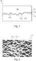
- Figure 1 shows a cross-sectional view of a bypass capacitance structure being realized by means of a conformal foil 100.
- the conformal foil 100 comprises an electrically conductive film structure 110 which is realized by a thin layer of conductive material such as copper.
- the electrically conductive film structure 110 has a rough surface 111 which exhibits a spatially irregular shape with valleys 111a and peaks 111b.
- the conformal foil 100 comprises a dielectric layer 130 conformally formed on the rough surface 111.
- the dielectric film structure 130 is realized by means of a thin layer of dielectric material. According to the exemplary embodiment described here the dielectric film structure 130 has a uniform thickness.
- the conformal foil 100 comprises a further electrically conductive film structure 120 being formed on the dielectric film structure 130.
- the dielectric film structure 130 is sandwiched between the electrically conductive film structure 110 and the further electrically conductive film structure 120.
- the further electrically conductive film structure 120 comprises a further rough surface 131, which is formed conformally on the dielectric film structure 130.
- the further rough surface 131 also exhibits a spatially irregular shape.
- the dielectric film structure 130 must comprise two rough surfaces.
- the roughening of the electrically conductive film structures 110, 120 increases the capacitance of the conformal foil 100.
- Figure 2 shows an electron-microscopic image of the rough surface 111 of the conformal foil depicted in Figure 1 .
- Valleys 111a and peaks 111b are visible. These peaks 111b and valleys 111a are distributed randomly and there is no spatial periodicity visible. This means that the rough surface 111 exhibits an irregular shape.
- Figure 3 shows in a cross-sectional view a bypass capacitance structure 300 being realized by a conformal foil, wherein an upper electrically conductive film structure 320 of the bypass capacitance structure 300 is spatially structured with recesses or gaps 340, 341. Due to the gaps 340, 341 different conductive material portions 321, 322, 323 are formed. Provided that there is an appropriate electrical connection (not shown) to the material portions 321, 322, 323 each one these material portions 321, 322, 323 forms part of the bypass capacitance structure.
- Figure 4 shows in a cross-sectional view an intermediate step when forming a component carrier 450 according to an embodiment of the invention.
- the conformal structured foil 300 is placed upside down onto a layered structure 460 representing at least a part of the component carrier 450.
- the layered structure 460 is a stack comprising an electrically insulating layer 462, an electrically conductive layer 464, a further electrically insulating layer 466, and a further electrically conductive layer 468. It is mentioned that the number of layers of the stack 460 is not limited to the described embodiment.
- the electrically conductive layers 464, 468 may be spatially structured. Further, not depicted vias may be formed within the electrically insulating layers 466, 468.
- Figure 5 shows in a cross-sectional view an electric system 580 comprising a component carrier 550 and an electronic component 590 mounted on the upper surface of the component carrier 550.
- the component carrier 550 comprises two stacks respectively two layered structures 560a, 560b. Each one of these two stacks 560a, 560b comprises at least one electrically insulating layer and at least one electrically conductive layer.
- the electrically conductive layer exhibit a spatial structuring and metallic interconnections are formed in order to realize an appropriate three dimensional conductor structure extending through the component carrier 450.
- the stack layers and the metallic interconnections are not denominated with reference numerals.
- a bypass capacitance structure realized by a conformal foil 300 which is sandwiched by the two stacks 560a, 560b. Further, the conformal foil 300 is horizontally subdivided in different portions.
- the component carrier 450 is an electronic interconnection device, which is connected to terminals 592 of the electronic component 590.
- terminals 592 of the electronic component 590 At a lower side of the electronic interconnection device 450 there are provided (ball shaped) terminals 594 which are electrically connected to the terminals 592 in an application specific appropriate manner.
- electrical signals may be transported between the terminals 592 of the electronic component 590 and the (ball shaped) terminals 594 via the (various portions of the) conformal foil 300, via appropriate metallic interconnects and via appropriately structured electrically conductive layers of the two stacks 560a and 560b.
- one of the electrically conductive film structure 110 and the further electrically conductive film structure 320 is assigned to a voltage supply plane of the electric system 580.
- the other one of the electrically conductive film structure 110 and the further electrically conductive film structure 320 is assigned to electric ground plane of the electric system 580.
- the capacitance of the conformal foil 300 provides for a timely smoothening of the level of the supply voltage.
- the signal integrity of signals, in particular fast digital AC signals, propagating within the electronic interconnection device 450 will be increased due to the capacitance of the bypass capacitance structure 300 being realized by means of the conformal foil 300.
- the described surface roughening of the electrically conductive film structures 110, 320 contributes to a high capacitance which increases the signal integrity.
Landscapes
- Engineering & Computer Science (AREA)
- Microelectronics & Electronic Packaging (AREA)
- Physics & Mathematics (AREA)
- Electromagnetism (AREA)
- Manufacturing & Machinery (AREA)
- Fixed Capacitors And Capacitor Manufacturing Machines (AREA)
- Geometry (AREA)
Abstract
Description
- The present invention generally relates to the technical field of component carriers onto which electronic components can be placed in order to form an electronic assembly. In particular, the present invention relates to a component carrier comprising a bypass capacitor.
- High-speed digital circuits typically present serious challenges related to the design of a power supply. For example, numerous logic gates are rapidly turned on and off and short surges of current are continuously drawn from an electrically conductive layer being associated with a power supply. Voltage regulators are often unable to adequately supply current for these surges. This often results in unwanted noise being present at voltage rails that can impair the functionality of electronic circuits or even result in total failure of electronic circuits.
- A known solution to the problems mentioned above is the use of a bypass capacitor, which acts like a small, low-impedance power supply for all the short surges of current, in particular switching current being associated with switching a digital electronic component. Therefore, many component carriers need a plurality of bypass capacitors, which are strategically placed on or within the component carrier. In this respect, the most important parameter of an appropriate bypass capacitor is its ability to supply a current instantaneously when such a current is needed.
- Bypass capacitors are typically realized by means of discrete electronic components. However, such discrete bypass capacitors regularly exhibit an internal parasitic inductance which limits their ability to rapidly supply an appropriate amount of current. This has a negative impact on the propagation and/or advancement of high frequency signals such as e.g. signals having fast clock rate.
- A common method for forming (bypass) capacitances on or within a component carrier is to place a thin layer of FR-4 material between two conductive layers. For instance a commonly used FR-4 core between copper conductive layers comprises a capacitance of about 50 pF per square inch.
- There may be a need for proving a component carrier with a bypass capacitor having an large capacitance.
- This need may be met by the subject matter according to the independent claims. Advantageous embodiments of the present invention are described by the dependent claims.
- According to a first aspect of the invention there is provided a component carrier comprising (a) a stack of at least one electrically conductive layer structure and at least one electrically insulating layer structure; and (b) a bypass capacitance structure formed on and/or within the stack. The bypass capacitance structure comprises an electrically conductive film structure having a rough surface, a dielectric film structure formed on the rough surface, and a further electrically conductive film structure formed on the dielectric film structure.
- The described component carrier is based on the idea that by forming a capacitance structure comprising or consisting of two electrically conductive film structures and one dielectric film structure sandwiched in between the two electrically conductive film structures a build-up structural arrangement can be created which can be used as a bypass capacitance structure for a component carrier. The dielectric film structure may be realized by means of a microscopic coating layer made from a highly insulating material (for example a dielectric metal oxide). In accordance with the described invention at least the electrically conductive film structure is provided with a rough surface such that the effective surface for the bypass capacitance structure will be increased.
- The rough surface may exhibit a spatially regular shape. Preferably, the rough surface exhibits a spatially irregular shape which may have the advantage that it will be much easier to find an appropriate physical or chemical treatment procedure in order to form the rough surface.
- Within the component carrier the bypass capacitance structure can be realized respectively used as a high capacitance power supply plane for digital circuits. Due to the roughened interface surface at least between the electrically conductive film structure and the dielectric film structure a significant increase of the specific surface area can be achieved. This results in a highly increased capacitance of the power supply plane. In accordance with basic principles of electronic circuits a high capacitance of a power supply plane has the positive effect that even in case of high-frequency digital signals propagating within or at the component carrier there will be enough short-term supply current available for compensating short surges of current which are drawn from the power supply plane. As has already been mentioned above, such surges may be associated with a switching operation of digital electronic components.
- As a quantitative example with regard to the value of the capacitance structure one may consider the capacitance C of a parallel-plate capacitor constructed of two parallel plates both of area A and separated from each other by a distance d:
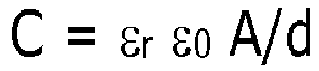
- Thereby, εr is the relative static permittivity (sometimes called the dielectric constant) of the material between the two plates (for a vacuum, εr = 1) and εr is the dielectric constant (= 8.854x 10⁻¹² As/Vm).
- From the above formula one can take that the capacitance C is proportional to the area A of the overlap between the electrically conductive film structure and the further electrically conductive film structure. Further, the capacitance C is inversely proportional to the separation d between the electrically conductive film structure and the further electrically conductive film structure. The closer the two electrically conductive film structures are the larger the capacitance C is.
- The described component carrier may rely on an embedded capacitance technology which may allow for a microscopic thin dielectric layer conformal deposited on a roughened interface surface between the two mentioned electrically conductive film structures. Within the design of the described component carrier the two electrically conductive film structures may be used as two conductor planes providing for a durable source of distributive decoupling capacitance structures. These two conductor planes can then take the place of conventional discrete (bypass) capacitors.
- At this point it is mentioned that in particular in case the stack comprises a plurality of layers with an alternating sequence of electrically conductive layer structures and electrically insulating layer structures there may be provided, within or between different layer structures, altogether more than one bypass capacitance structure as described above. This may allow to provide in an easy and effective manner a compensation for current surge demands at different locations within the described component carrier.
- In the context of this document, the term "component carrier" may particularly denote any type of support structure which is capable of accommodating one or more electronic components thereon and/or therein for providing both mechanical support and electrical connectivity. The component carrier may be for instance a PCB or generally any type of flexible, semi-flexible or rigid substrate.
- With the described component carrier the capacitance overlap area between different electrically conductive films or different electrically conductive film structures can be reduced while providing for the same capacitance value. This may allow for realizing different voltage levels within a single split voltage plane layer, leading to a reduced layer count and lower cost. Further, parasitic inductances, which are in particular yielded by discrete bypass capacitors, can be reduced. The same holds for an unwanted crosstalk between different signals propagating along spatially neighboring conductor tracks. As a consequence, and improved signal integrity in particular at higher signal clock rates can be provided.
- The described bypass capacitance structure may be formed at different locations in or at the component carrier. For instance, the bypass capacitance structure can be applied directly on top of the component carrier as an outlay. Further, the bypass capacitance structure can be used as a core layer of and within the component carrier. Furthermore, the bypass capacitance structure may be realized as a sequential build-up structure within a known Every Layer Interconnection (ELIC) process for manufacturing the component carrier. All these possibilities allow for a great freedom of design in particular with respect to a provision of the required voltage stability of high speed signal connections at any location of an electronic assembly respectively circuit formed at and/or within the described component carrier.
- According to an embodiment of the invention the rough surface has an effective surface area which, compared to a corresponding planar surface area, is larger by a factor of 1.2 and in particular larger by a factor in a range between 1.5 and 30. By this way, compared to a not roughened surface, the capacitance can be increased by the same amount.
- According to a further embodiment of the invention the rough surface comprises an average peak-to-valley height value, Rz, of 1 µm to 50 µm, in particular 1 µm to 25 µm, more particularly 2 µm to 9 µm.
- According to the above given formula C = εr εo A/d, the larger the area A is, the larger is the capacitance C. Thus, the larger the average peak-to-valley height value Rz is, the larger may be the surface area.
- When the rough surface is viewed in a cross-sectional view, a "landscape" of peak and valley shapes may be visible. In this respect, Rpm may be the average maximum peak height, which is found by averaging the heights of the highest peaks. Rvm, may be the average maximum valley depth, which is found by averaging the depths of the lowest valleys. Rz, may then be described as Rpm-Rvm.
- According to a further embodiment of the invention the dielectric film structure comprises a thickness which is in the range between 10 nm and 2000 nm, in particular lower than 1000 nm.
- According to the above given formula C = εr εo A/d, the closer the respective sheets respectively the electrically conductive film structures are located with respect to each other, the greater is the capacitance C. A very high Rz value of the rough surface together with a very thin dielectric layer may provide a very high capacitance.
- According to a further embodiment of the invention the dielectric film structure comprises a material having a dielectric constant which is in the range between 3 and 1000 and in particular between 6 and 1000.
- According to the above given formula C = εr εo A/d, the higher the dielectric constant εo, also termed relative permittivity, of the dielectric layer is, the larger is the capacitance C.
- Permittivity is directly related to electric susceptibility, which is a measure of how easy a dielectric material is getting polarized in response to an impacting external electric field. In international system (SI) units, the permittivity ε is measured in Farads per meter (F/m) and the electric susceptibility X is without a dimension. Permittivity and susceptibility are related to each other according to the formula ε = εr εo = (1 + X) ε0, wherein εr is the relative permittivity or dielectric constant of the material, and ε0 = 8.8541878176 × 10⁻¹² F/m is the vacuum permittivity. The dielectric constant value of FR-4, which is a typical electrically insulating material of a component carrier such as printed circuit board (PCB), is 4.2. Materials such as CaCu3Ti4O12 and various members of the series Ln2/3Cu3Ti4O12 with Ln = La, Ce, Pr, Nd, Sm, Eu, Gd, Tb, Dy, Ho, Er and Tm may have an extremely high value for its dielectric constant.
- According to a further embodiment of the invention the dielectric film structure comprises a material selected from a group consisting of diamond-like carbon, aluminum oxide, silicon nitride, silicon oxide, neodymium oxide, hafnium oxide, zirconium oxide, or a combination of these materials.
- The dielectric constants εr of these materials is comparatively high. The dielectric constant for diamond-like carbon is approximately 3, for aluminum oxide approximately 9, for silicon nitride approximately 7, for silicon oxide approximately 3.9, for hafnium oxide approximately 25 and for zirconium oxide approximately 25. All these materials are suitable for manufacturing the bypass capacitance structure and allow for a large capacitance.
- According to a further embodiment of the invention the dielectric film structure has been formed by chemical vapor deposition and/or by physical vapor deposition and/or by galvanic coating and/or by electrophoresis.
- Chemical vapor deposition (CVP) is a chemical process which is often used to produce high quality, high-performance, solid materials. CVP may include more specific processes such as atmospheric pressure CVD (APCVD), low-pressure CVD (LPCVD), or ultrahigh vacuum CVD (UHVCVD).
- Physical vapor deposition (PVD) describes a variety of vacuum deposition methods used to deposit thin films by the condensation of a vapor comprising the desired film material at various surfaces. Such a coating involves purely physical processes such as high-temperature vacuum evaporation with subsequent condensation, or plasma sputter bombardment rather than involving a chemical reaction at the surface to be coated as in CVP.
- The dielectric film structure may be conformally formed on or over the electrically conductive layer. Every region of the rough surface of the electrically conductive layer may be coated by means of a vapor deposition with the same amount of dielectric material. Thus, every peak of the rough surface and every valley of the rough surface of the electrically conductive film structure may be coated with the same amount respectively thickness of dielectric material. As a consequence, the dielectric layer comprises at least approximately a uniform thickness.
- It is mentioned that the dielectric film structure can also be formed with other known methods such as for example RF sputtering, RF reactive sputtering, DC reactive sputtering utilizing a pulsed DC power supply, etc.
- According to a further embodiment of the invention the further electrically conductive film comprises a further rough surface. This may mean that there will be a rough interface surface also between the dielectric film structure and the further electrically conductive film structure. According to exemplary embodiments also the further rough surface may exhibit a spatially irregular shape.
- According to a further embodiment of the invention the further rough surface is formed conformally at the dielectric film structure.
- The further electrically conductive material may be directly formed on or at the dielectric film structure, for example by means of CVD or PVD methods. The bottom side of the dielectric film structure, which is conformally formed on or at the rough surface of the electrically conductive film structure, may comprise an irregular shaped surface. Because the dielectric film structure comprises a uniform thickness, also the top side of the dielectric film structure, which is opposite to the bottom side of the dielectric film structure, exhibits an irregular shaped surface. When the further electrically conductive material is formed on or at the dielectric film structure, the further rough surface is then conformally formed on or at the dielectric layer.
- According to a further embodiment of the invention the further rough surface comprises at least approximately the same average peak-to-valley height value, Rz, as the rough surface. This may provide the advantage that the capacitance of the bypass capacitance structure may be further increased by the further rough surface.
- According to a further embodiment of the invention the at least one electrically conductive layer structure, the electrically conductive film structure and/or the further electrically conductive film structure comprises at least one material of the group consisting of copper, aluminum, and nickel. Also this may provide the advantage that the described bypass capacitance structure with its advantageous effects and also the entire component carrier can be realized by employing well known and approved process technologies.
- According to a further embodiment of the invention the electrically conductive film structure is assigned to an electrical power supply plane layer at or within the component carrier and/or the further electrically conductive film structure is assigned to an electrical ground plane layer. This may provide the advantage that the large capacitance being provided by the described bypass capacitance structure can be effectively used for providing a very stable supply voltage for any electronic component being mounted within or at the described component carrier.
- According to a further embodiment of the invention the at least one electrically insulating layer structure comprises at least one of the group consisting of resin, in particular Bismaleimide-Triazine resin, cyanate ester, glass, in particular glass fibers, prepreg material, polyimide, liquid crystal polymer, epoxy-based Build-Up Film, FR4 material, a ceramic, and a metal oxide.
- According to a further embodiment of the invention the component carrier is shaped as a plate. This may contribute to a compact design of the component carrier which nevertheless provides a large basis for mounting electronic components thereon.
- According to a further embodiment of the invention the component carrier is configured as one of the group consisting of a printed circuit board and a substrate.
- In the context of this document, the term "printed circuit board" (PCB) may particularly denote a plate-shaped component carrier which is formed by laminating several electrically conductive layer structures with several electrically insulating layer structures, for instance by applying pressure, if desired accompanied by the supply of thermal energy. As preferred materials for PCB technology, the electrically conductive layer structures are made of copper, whereas the electrically insulating layer structures may comprise resin and/or glass fibers, so-called prepreg or FR4 material. The various electrically conductive layer structures may be connected to one another in a desired way by forming through-holes through the laminate, for instance by laser drilling or mechanical drilling, and by filling them with electrically conductive material (in particular copper), thereby forming vias as through-hole connections. Apart from one or more electronic components which may be embedded in a printed circuit board, a printed circuit board is usually configured for accommodating one or more electronic components on one or both opposing surfaces of the plate-shaped printed circuit board. They may be connected to the respective main surface by soldering.
- In the context of this document, the term "substrate" may particularly denote a small component carrier having substantially the same size as an electronic component to be mounted thereon. A component carrier may also be a so called intermediate carrier which can be used as an adapter for spatially spreading contact terminals being formed at an electronic component, in particular a bare die, such that the electronic component can be contacted with contact pads formed e.g. at a PCB.
- According to a further embodiment of the invention the component carrier is a laminate-type component carrier. In such an embodiment, the component carrier is a compound of multiple layer structures which are stacked and connected together by applying a pressing force, if desired accompanied by heat.
- According to a further aspect of the invention there is provided an electronic system comprising a component carrier as described above; and an electronic component. The electronic component is embedded in the component carrier. An embedded component may provide the advantage that the integration level for an electronic circuit assembly being mounted to the component carrier can be increased when connecting embedded electronic component in such a manner that it forms a part of the electronic circuit.
- According to a further embodiment of the invention the electronic component may be selected from a group consisting of an active electronic component, a passive electronic component, an electronic chip, a storage device, a filter, an integrated circuit, a signal processing component, a power management component, an optoelectronic interface element, a voltage converter, a cryptographic component, a transmitter and/or receiver, an electromechanical transducer, a sensor, an actuator, a microelectromechanical system, a microprocessor, a capacitor, a resistor, an inductance, a battery, a switch, a camera, an antenna, a magnetic element, and a logic chip.
- According to a further aspect of the invention there is provided a method for manufacturing a component carrier, the method comprising (a) forming a stack of at least one electrically conductive layer structure and at least one electrically insulating layer structure; and (b) arranging a bypass capacitance structure on an/or within the stack, wherein the bypass capacitance structure is formed with an electrically conductive film structure having a rough surface, a dielectric film structure on the rough surface, and a further electrically conductive film structure formed on the dielectric film structure.
- Also the described method is based on the idea that by forming a capacitance structure comprising or consisting of two electrically conductive film structures and a dielectric film structure sandwiched in between these electrically conductive film structures a build-up structural arrangement can be created which can be used as a bypass capacitance structure for a component carrier and which can be integrally formed within the component carrier.
- The described manufacturing method can be implemented within a standard High Density Interconnection (HDI) process and/or any many other substrate manufacturing processes.
- The dielectric film structure may be deposited roll to roll in a cost effective web process.
- It has to be noted that embodiments of the invention have been described with reference to different subject matters. In particular, some embodiments have been described with reference to a component carrier whereas other embodiments have been described with reference to a method for manufacturing such a component carrier. However, a person skilled in the art will gather from the above and the following description that, unless other notified, in addition to any combination of features belonging to one type of subject matter also any combination between features relating to different subject matters (i.e. component carrier and method) is considered as to be disclosed with this technical description of the invention.
- The aspects defined above and further aspects of the present invention are apparent from the examples of embodiment to be described hereinafter and are explained with reference to the examples of embodiment. The invention will be described in more detail hereinafter with reference to examples of embodiment but to which the invention is not limited.
-
- Figure 1
- shows a cross-sectional view of a bypass capacitance structure being realized by means of a conformal foil.
- Figure 2
- shows an electron-microscopic image of a rough surface of the conformal foil depicted in
Figure 1 . - Figure 3
- shows in a cross-sectional view a bypass capacitance structure, wherein one electrically conductive film structure of the bypass ca-pacitance structure is spatially structured with recesses.
- Figure 4
- shows in a cross-sectional view an intermediate step when forming a component carrier according to an embodiment of the invention.
- Figure 5
- shows in a cross-sectional view an electric system comprising an electronic component is mounted on a component carrier comprising an embedded bypass capacitance structure being realized by means of a conformal foil.
- The illustration in the drawing is schematic. It is noted that in different figures, similar or identical elements or features are provided with the same reference signs. In order to avoid unnecessary repetitions elements or features which have already been elucidated with respect to a previously described embodiment are not elucidated again at a later position of the description.
- Further, spatially relative terms, such as "front" and "back", "above" and "below", "left" and "right", et cetera are used to describe an element's relationship to another element(s) as illustrated in the figures. Thus, the spatially relative terms may apply to orientations in use which differ from the orientation depicted in the figures. Obviously all such spatially relative terms refer to the orientation shown in the figures only for ease of description and are not necessarily limiting as an apparatus according to an embodiment of the invention can assume orientations different than those illustrated in the figures when in use.
-
Figure 1 shows a cross-sectional view of a bypass capacitance structure being realized by means of aconformal foil 100. Theconformal foil 100 comprises an electricallyconductive film structure 110 which is realized by a thin layer of conductive material such as copper. The electricallyconductive film structure 110 has arough surface 111 which exhibits a spatially irregular shape withvalleys 111a and peaks 111b. - Further, the
conformal foil 100 comprises adielectric layer 130 conformally formed on therough surface 111. Thedielectric film structure 130 is realized by means of a thin layer of dielectric material. According to the exemplary embodiment described here thedielectric film structure 130 has a uniform thickness. - Furthermore, the
conformal foil 100 comprises a further electricallyconductive film structure 120 being formed on thedielectric film structure 130. Thedielectric film structure 130 is sandwiched between the electricallyconductive film structure 110 and the further electricallyconductive film structure 120. - The further electrically
conductive film structure 120 comprises a furtherrough surface 131, which is formed conformally on thedielectric film structure 130. The furtherrough surface 131 also exhibits a spatially irregular shape. - It should be clear for a person skilled in the art that due to the conformal interfaces between (a) the "rough" electrically
conductive film structure 110 and thedielectric film structure 130 and (b) thedielectric film structure 130 and the "rough" further electricallyconductive film structure 120 thedielectric film structure 130 must comprise two rough surfaces. In accordance with basic physical principles the roughening of the electricallyconductive film structures conformal foil 100. -
Figure 2 shows an electron-microscopic image of therough surface 111 of the conformal foil depicted inFigure 1 .Valleys 111a and peaks 111b are visible. Thesepeaks 111b andvalleys 111a are distributed randomly and there is no spatial periodicity visible. This means that therough surface 111 exhibits an irregular shape. -
Figure 3 shows in a cross-sectional view abypass capacitance structure 300 being realized by a conformal foil, wherein an upper electricallyconductive film structure 320 of thebypass capacitance structure 300 is spatially structured with recesses orgaps gaps conductive material portions material portions material portions -
Figure 4 shows in a cross-sectional view an intermediate step when forming acomponent carrier 450 according to an embodiment of the invention. As can be taken from this Figure, the conformalstructured foil 300 is placed upside down onto alayered structure 460 representing at least a part of thecomponent carrier 450. According to the exemplary embodiment described here thelayered structure 460 is a stack comprising an electrically insulatinglayer 462, an electricallyconductive layer 464, a further electrically insulatinglayer 466, and a further electricallyconductive layer 468. It is mentioned that the number of layers of thestack 460 is not limited to the described embodiment. The electricallyconductive layers layers -
Figure 5 shows in a cross-sectional view anelectric system 580 comprising acomponent carrier 550 and anelectronic component 590 mounted on the upper surface of thecomponent carrier 550. Thecomponent carrier 550 comprises two stacks respectively twolayered structures stacks Figure 5 , the electrically conductive layer exhibit a spatial structuring and metallic interconnections are formed in order to realize an appropriate three dimensional conductor structure extending through thecomponent carrier 450. For the sake of clarity of the illustration the stack layers and the metallic interconnections are not denominated with reference numerals. - As can be seen from
Figure 5 , a bypass capacitance structure realized by aconformal foil 300 which is sandwiched by the twostacks conformal foil 300 is horizontally subdivided in different portions. - According to the exemplary embodiment described here the
component carrier 450 is an electronic interconnection device, which is connected toterminals 592 of theelectronic component 590. At a lower side of theelectronic interconnection device 450 there are provided (ball shaped)terminals 594 which are electrically connected to theterminals 592 in an application specific appropriate manner. In this way, electrical signals may be transported between theterminals 592 of theelectronic component 590 and the (ball shaped)terminals 594 via the (various portions of the)conformal foil 300, via appropriate metallic interconnects and via appropriately structured electrically conductive layers of the twostacks - According to the exemplary embodiment described here one of the electrically
conductive film structure 110 and the further electricallyconductive film structure 320 is assigned to a voltage supply plane of theelectric system 580. The other one of the electricallyconductive film structure 110 and the further electricallyconductive film structure 320 is assigned to electric ground plane of theelectric system 580. As has already been mention above in the general description of embodiments of the invention the capacitance of theconformal foil 300 provides for a timely smoothening of the level of the supply voltage. As a consequence, the signal integrity of signals, in particular fast digital AC signals, propagating within theelectronic interconnection device 450 will be increased due to the capacitance of thebypass capacitance structure 300 being realized by means of theconformal foil 300. The described surface roughening of the electricallyconductive film structures - It should be noted that the term "comprising" does not exclude other elements or steps and the use of articles "a" or "an" does not exclude a plurality. Also elements described in association with different embodiments may be combined. It should also be noted that reference signs in the claims should not be construed as limiting the scope of the claims.
-
- 100
- bypass capacitance structure / conformal foil
- 110
- electrically conductive film structure
- 111
- rough surface
- 111a
- rough surface valley
- 111b
- rough surface peak
- 120
- further electrically conductive film structure
- 130
- dielectric film structure
- 131
- further rough surface
- 300
- bypass capacitance structure / conformal foil
- 320
- further electrically conductive film structure
- 321
- conductive material portion
- 322
- conductive material portion
- 323
- conductive material portion
- 340
- recess
- 341
- further recess
- 450
- component carrier / electronic interconnection device
- 460
- layered structure / stack
- 462
- electrically insulating layer
- 464
- electrically conductive layer
- 466
- further electrically insulating layer
- 468
- further electrically conductive layer
- 550
- component carrier
- 560a
- layered structure / stack
- 560b
- layered structure / stack
- 580
- electric system
- 590
- electronic component
- 592
- terminals
- 594
- (ball shaped) terminals
Claims (15)
- A component carrier, comprising:a stack (460, 560a, 560b) of at least one electrically conductive layer structure (464, 468) and at least one electrically insulating layer structure (462, 466); anda bypass capacitance structure (100, 300) formed on and/or within the stack (460, 560a, 560b);wherein the bypass capacitance structure (100, 300) comprises an electrically conductive film structure (110) having a rough surface (111a), a dielectric film structure (130) formed on the rough surface (111a), and a further electrically conductive film structure (120, 320) formed on the dielectric film structure (130).
- The component carrier as set forth in the preceding claim, wherein
the rough surface (111a) has an effective surface area which, compared to a corresponding planar surface area, is larger by a factor of at least 1.2, and in particular is larger by a factor in a range between 1.5 and 30. - The component carrier as set forth in any one of the preceding claims, wherein
the rough surface (111a) comprises an average peak-to-valley height value, Rz, of 1 µm to 50 µm, in particular 1 µm to 25 µm, more particularly 2 µm to 9 µm. - The component carrier as set forth in any one of the preceding claims, wherein
the dielectric film structure (130) comprises a thickness which is in the range between 10 nm and 2000 nm, in particular lower than 1000 nm. - The component carrier as set forth in any one of the preceding claims, wherein
the dielectric film structure (130) comprises a material having a dielectric constant which is in the range between 3 and 1000. - The component carrier as set forth in any one of the preceding claims, wherein
the dielectric film structure (130) comprises a material selected from a group consisting of diamond-like carbon, aluminum oxide, silicon nitride, silicon oxide, neodymium oxide, hafnium oxide, zirconium oxide, or a combination of these materials and/or
the dielectric film structure (130) has been formed by chemical vapor deposition and/or by physical vapor deposition and/or by galvanic coating and/or by electrophoresis. - The component carrier as set forth in any one of the preceding claims, wherein
the further electrically conductive film (120, 320) comprises a further rough surface (131). - The component carrier as set forth in the preceding claim, wherein
the further rough surface (131) is formed conformally at the dielectric film structure (130). - The component carrier as set forth in any one of the preceding claims 7 and 8, wherein
the further rough surface (131) comprises at least approximately the same average peak-to-valley height value, Rz, as the rough surface (111). - The component carrier as set forth in any one of the preceding claims, wherein
the at least one electrically conductive layer structure (464, 468), the electrically conductive film structure (110) and/or the further electrically conductive film structure (120) comprises at least one material of the group consisting of copper, aluminum, and nickel. - The component carrier as set forth in any one of the preceding claims, wherein
the electrically conductive film structure (110) is assigned to an electrical power supply plane layer at or within the component carrier (450, 550) and/or
the further electrically conductive film structure (120) is assigned to an electrical ground plane layer. - The component carrier as set forth in any one of the preceding claims, wherein
the at least one electrically insulating layer structure (462, 466) comprises at least one of the group consisting of resin, in particular Bismaleimide-Triazine resin, cyanate ester, glass, in particular glass fibers, prepreg material, polyimide, liquid crystal polymer, epoxy-based Build-Up Film, FR4 material, a ceramic, and a metal oxide. - The component carrier as set forth in any one of the preceding claims, wherein
the component carrier (450, 550) is shaped as a plate and/or
the component carrier (450, 550) is configured as one of the group consisting of a printed circuit board and a substrate and/or
the component carrier (450, 550) is a laminate-type component carrier. - An electronic system comprisinga component carrier (450, 550) according to any one of the preceding claims; andan electronic component (500);wherein the electric component (500) is mounted at the component carrier (300).
- The electronic system according to claim 14, wherein
the electronic component (500) is selected from a group consisting of an active electronic component, a passive electronic component, an electronic chip, a storage device, a filter, an integrated circuit, a signal processing component, a power management component, an optoelectronic interface element, a voltage converter, a cryptographic component, a transmitter and/or receiver, an electromechanical transducer, a sensor, an actuator, a microelectromechanical system, a microprocessor, a capacitor, a resistor, an inductance, a battery, a switch, a camera, an antenna, a magnetic element, and a logic chip.
Applications Claiming Priority (1)
| Application Number | Priority Date | Filing Date | Title |
|---|---|---|---|
| CN201610619075.7A CN107665879A (en) | 2016-07-29 | 2016-07-29 | Component carrier and the electronic system for including the component carrier |
Publications (2)
| Publication Number | Publication Date |
|---|---|
| EP3277064A1 true EP3277064A1 (en) | 2018-01-31 |
| EP3277064B1 EP3277064B1 (en) | 2021-12-08 |
Family
ID=59655871
Family Applications (1)
| Application Number | Title | Priority Date | Filing Date |
|---|---|---|---|
| EP17183864.2A Active EP3277064B1 (en) | 2016-07-29 | 2017-07-28 | Component carrier with a bypass capacitance comprising dielectric film structure and method of fabrication for such component carrier |
Country Status (3)
| Country | Link |
|---|---|
| US (1) | US10568208B2 (en) |
| EP (1) | EP3277064B1 (en) |
| CN (1) | CN107665879A (en) |
Families Citing this family (1)
| Publication number | Priority date | Publication date | Assignee | Title |
|---|---|---|---|---|
| EP4651635A1 (en) * | 2024-05-14 | 2025-11-19 | Rimac Technology LLC | Pcb layer stack-up and floor planning |
Citations (1)
| Publication number | Priority date | Publication date | Assignee | Title |
|---|---|---|---|---|
| EP1699275A2 (en) * | 2005-03-02 | 2006-09-06 | Samsung Electro-mechanics Co., Ltd | Printed circuit board with embedded capacitors therein and manufacturing process thereof |
Family Cites Families (16)
| Publication number | Priority date | Publication date | Assignee | Title |
|---|---|---|---|---|
| US5431963A (en) * | 1993-02-01 | 1995-07-11 | General Electric Company | Method for adhering diamondlike carbon to a substrate |
| US5844770A (en) * | 1997-08-21 | 1998-12-01 | K Systems Corporation | Capacitor structures with dielectric coated conductive substrates |
| IL132834A (en) | 1998-11-23 | 2006-06-11 | Micro Coating Technologies | Formation of thin film capacitors |
| US6274224B1 (en) * | 1999-02-01 | 2001-08-14 | 3M Innovative Properties Company | Passive electrical article, circuit articles thereof, and circuit articles comprising a passive electrical article |
| EP1100295B1 (en) | 1999-11-12 | 2012-03-28 | Panasonic Corporation | Capacitor-mounted metal foil and a method for producing the same, and a circuit board and a method for producing the same |
| US6847527B2 (en) * | 2001-08-24 | 2005-01-25 | 3M Innovative Properties Company | Interconnect module with reduced power distribution impedance |
| JP3711343B2 (en) * | 2002-06-26 | 2005-11-02 | 株式会社トッパンNecサーキットソリューションズ | Printed wiring board, manufacturing method thereof, and semiconductor device |
| KR100455891B1 (en) * | 2002-12-24 | 2004-11-06 | 삼성전기주식회사 | A printed circuit board with embedded capacitors, and a manufacturing process thereof |
| US20060022304A1 (en) * | 2004-07-29 | 2006-02-02 | Rohm And Haas Electronic Materials Llc | Dielectric structure |
| US7190016B2 (en) | 2004-10-08 | 2007-03-13 | Rohm And Haas Electronic Materials Llc | Capacitor structure |
| EP2445107B1 (en) * | 2004-12-09 | 2019-02-20 | Wispry, Inc. | Pole-zero elements and related systems and methods |
| US9572258B2 (en) * | 2004-12-30 | 2017-02-14 | Intel Corporation | Method of forming a substrate core with embedded capacitor and structures formed thereby |
| US20060220167A1 (en) * | 2005-03-31 | 2006-10-05 | Intel Corporation | IC package with prefabricated film capacitor |
| KR100967056B1 (en) | 2007-03-29 | 2010-06-29 | 삼성전기주식회사 | Thin Film Capacitors and Printed Circuit Boards with Thin Film Capacitors |
| KR100898974B1 (en) * | 2007-06-18 | 2009-05-25 | 삼성전기주식회사 | Thin Film Capacitors, Laminated Structures and Manufacturing Method Thereof |
| US8088658B2 (en) * | 2009-04-28 | 2012-01-03 | E. I. Du Pont De Nemours And Company | Thin film capacitor and method of fabrication thereof |
-
2016
- 2016-07-29 CN CN201610619075.7A patent/CN107665879A/en active Pending
-
2017
- 2017-07-28 EP EP17183864.2A patent/EP3277064B1/en active Active
- 2017-07-28 US US15/662,406 patent/US10568208B2/en not_active Expired - Fee Related
Patent Citations (1)
| Publication number | Priority date | Publication date | Assignee | Title |
|---|---|---|---|---|
| EP1699275A2 (en) * | 2005-03-02 | 2006-09-06 | Samsung Electro-mechanics Co., Ltd | Printed circuit board with embedded capacitors therein and manufacturing process thereof |
Also Published As
| Publication number | Publication date |
|---|---|
| US20180035543A1 (en) | 2018-02-01 |
| CN107665879A (en) | 2018-02-06 |
| US10568208B2 (en) | 2020-02-18 |
| EP3277064B1 (en) | 2021-12-08 |
Similar Documents
| Publication | Publication Date | Title |
|---|---|---|
| KR100974634B1 (en) | Capacitor devices | |
| KR100227528B1 (en) | Capacitor laminate for printed circuit board | |
| US7733626B2 (en) | Passive device structure | |
| TWI321970B (en) | Package stucture with embedded capacitor and applications thereof | |
| EP3384529B1 (en) | Electronic device with a plurality of component carrier packages being electrically and mechanically connected electronic device having an integral electromagnetic shielding structure entirely surrounding the electronic device for providing hermetic shielding | |
| CN111816638B (en) | Component carrier including a double-layer structure and methods of making and using the double-layer structure | |
| EP4134992A1 (en) | Glass core wiring substrate with built-in high-frequency filter, high-frequency module in which said glass core wiring substrate with built-in high-frequency filter is used, and method for manufacturing glass core wiring substrate with built-in high-frequency filter | |
| US20180288879A1 (en) | Component Carrier and Manufacturing Method | |
| EP1153531A1 (en) | Passive electrical article, circuit articles thereof, and circuit articles comprising a passive electrical article | |
| JP2015076600A (en) | Multilayer ceramic electronic component to be embedded in board and multilayer ceramic electronic component embedded printed circuit board | |
| KR20080080788A (en) | Printed Circuit Board and Manufacturing Method for Improving Tolerance of Embedded Capacitor | |
| TWI455662B (en) | A method for manufacturing a capacitor-type printed wiring board, and a method for manufacturing the capacitor-type printed wiring board | |
| KR100678083B1 (en) | Embedded Capacitors and How to Make Embedded Capacitors | |
| US11589462B2 (en) | Semi-flexible component carrier with stepped layer structure | |
| EP3277064B1 (en) | Component carrier with a bypass capacitance comprising dielectric film structure and method of fabrication for such component carrier | |
| CN107231747A (en) | Electric capacity, bury condenser network plate and its manufacture method | |
| EP2496059B1 (en) | Printed wiring board with PWB-embedded capacitor mounted thereon and method for fabricating the same | |
| US20210059044A1 (en) | Electronic Device Having an Electronic Component Packaged in a Compact Component Carrier With Shielding Cavities | |
| US11219120B2 (en) | Stress relief opening for reducing warpage of component carriers | |
| TW200845843A (en) | Method for manufacturing printed circuit board with built-in capacitor | |
| US10109554B2 (en) | Mechanically stable, thermally conductive and electrically insulating stack forming a mounting device for electronic components | |
| CN209767902U (en) | Component carrier and plate | |
| CN107665878A (en) | Paper tinsel, the component carrier with paper tinsel and the electronic system with component carrier | |
| CN207382679U (en) | Capacitance and bury condenser network plate | |
| KR20060051538A (en) | Circuit board |
Legal Events
| Date | Code | Title | Description |
|---|---|---|---|
| PUAI | Public reference made under article 153(3) epc to a published international application that has entered the european phase |
Free format text: ORIGINAL CODE: 0009012 |
|
| STAA | Information on the status of an ep patent application or granted ep patent |
Free format text: STATUS: THE APPLICATION HAS BEEN PUBLISHED |
|
| AK | Designated contracting states |
Kind code of ref document: A1 Designated state(s): AL AT BE BG CH CY CZ DE DK EE ES FI FR GB GR HR HU IE IS IT LI LT LU LV MC MK MT NL NO PL PT RO RS SE SI SK SM TR |
|
| AX | Request for extension of the european patent |
Extension state: BA ME |
|
| STAA | Information on the status of an ep patent application or granted ep patent |
Free format text: STATUS: REQUEST FOR EXAMINATION WAS MADE |
|
| 17P | Request for examination filed |
Effective date: 20180711 |
|
| RBV | Designated contracting states (corrected) |
Designated state(s): AL AT BE BG CH CY CZ DE DK EE ES FI FR GB GR HR HU IE IS IT LI LT LU LV MC MK MT NL NO PL PT RO RS SE SI SK SM TR |
|
| STAA | Information on the status of an ep patent application or granted ep patent |
Free format text: STATUS: EXAMINATION IS IN PROGRESS |
|
| 17Q | First examination report despatched |
Effective date: 20200504 |
|
| GRAP | Despatch of communication of intention to grant a patent |
Free format text: ORIGINAL CODE: EPIDOSNIGR1 |
|
| STAA | Information on the status of an ep patent application or granted ep patent |
Free format text: STATUS: GRANT OF PATENT IS INTENDED |
|
| INTG | Intention to grant announced |
Effective date: 20210622 |
|
| GRAS | Grant fee paid |
Free format text: ORIGINAL CODE: EPIDOSNIGR3 |
|
| GRAA | (expected) grant |
Free format text: ORIGINAL CODE: 0009210 |
|
| STAA | Information on the status of an ep patent application or granted ep patent |
Free format text: STATUS: THE PATENT HAS BEEN GRANTED |
|
| AK | Designated contracting states |
Kind code of ref document: B1 Designated state(s): AL AT BE BG CH CY CZ DE DK EE ES FI FR GB GR HR HU IE IS IT LI LT LU LV MC MK MT NL NO PL PT RO RS SE SI SK SM TR |
|
| REG | Reference to a national code |
Ref country code: GB Ref legal event code: FG4D |
|
| REG | Reference to a national code |
Ref country code: AT Ref legal event code: REF Ref document number: 1454746 Country of ref document: AT Kind code of ref document: T Effective date: 20211215 Ref country code: CH Ref legal event code: EP |
|
| REG | Reference to a national code |
Ref country code: DE Ref legal event code: R096 Ref document number: 602017050495 Country of ref document: DE |
|
| REG | Reference to a national code |
Ref country code: IE Ref legal event code: FG4D |
|
| REG | Reference to a national code |
Ref country code: LT Ref legal event code: MG9D |
|
| REG | Reference to a national code |
Ref country code: NL Ref legal event code: MP Effective date: 20211208 |
|
| PG25 | Lapsed in a contracting state [announced via postgrant information from national office to epo] |
Ref country code: RS Free format text: LAPSE BECAUSE OF FAILURE TO SUBMIT A TRANSLATION OF THE DESCRIPTION OR TO PAY THE FEE WITHIN THE PRESCRIBED TIME-LIMIT Effective date: 20211208 Ref country code: LT Free format text: LAPSE BECAUSE OF FAILURE TO SUBMIT A TRANSLATION OF THE DESCRIPTION OR TO PAY THE FEE WITHIN THE PRESCRIBED TIME-LIMIT Effective date: 20211208 Ref country code: FI Free format text: LAPSE BECAUSE OF FAILURE TO SUBMIT A TRANSLATION OF THE DESCRIPTION OR TO PAY THE FEE WITHIN THE PRESCRIBED TIME-LIMIT Effective date: 20211208 Ref country code: BG Free format text: LAPSE BECAUSE OF FAILURE TO SUBMIT A TRANSLATION OF THE DESCRIPTION OR TO PAY THE FEE WITHIN THE PRESCRIBED TIME-LIMIT Effective date: 20220308 |
|
| REG | Reference to a national code |
Ref country code: AT Ref legal event code: MK05 Ref document number: 1454746 Country of ref document: AT Kind code of ref document: T Effective date: 20211208 |
|
| PG25 | Lapsed in a contracting state [announced via postgrant information from national office to epo] |
Ref country code: SE Free format text: LAPSE BECAUSE OF FAILURE TO SUBMIT A TRANSLATION OF THE DESCRIPTION OR TO PAY THE FEE WITHIN THE PRESCRIBED TIME-LIMIT Effective date: 20211208 Ref country code: NO Free format text: LAPSE BECAUSE OF FAILURE TO SUBMIT A TRANSLATION OF THE DESCRIPTION OR TO PAY THE FEE WITHIN THE PRESCRIBED TIME-LIMIT Effective date: 20220308 Ref country code: LV Free format text: LAPSE BECAUSE OF FAILURE TO SUBMIT A TRANSLATION OF THE DESCRIPTION OR TO PAY THE FEE WITHIN THE PRESCRIBED TIME-LIMIT Effective date: 20211208 Ref country code: HR Free format text: LAPSE BECAUSE OF FAILURE TO SUBMIT A TRANSLATION OF THE DESCRIPTION OR TO PAY THE FEE WITHIN THE PRESCRIBED TIME-LIMIT Effective date: 20211208 Ref country code: GR Free format text: LAPSE BECAUSE OF FAILURE TO SUBMIT A TRANSLATION OF THE DESCRIPTION OR TO PAY THE FEE WITHIN THE PRESCRIBED TIME-LIMIT Effective date: 20220309 Ref country code: ES Free format text: LAPSE BECAUSE OF FAILURE TO SUBMIT A TRANSLATION OF THE DESCRIPTION OR TO PAY THE FEE WITHIN THE PRESCRIBED TIME-LIMIT Effective date: 20211208 |
|
| PG25 | Lapsed in a contracting state [announced via postgrant information from national office to epo] |
Ref country code: NL Free format text: LAPSE BECAUSE OF FAILURE TO SUBMIT A TRANSLATION OF THE DESCRIPTION OR TO PAY THE FEE WITHIN THE PRESCRIBED TIME-LIMIT Effective date: 20211208 |
|
| PG25 | Lapsed in a contracting state [announced via postgrant information from national office to epo] |
Ref country code: SM Free format text: LAPSE BECAUSE OF FAILURE TO SUBMIT A TRANSLATION OF THE DESCRIPTION OR TO PAY THE FEE WITHIN THE PRESCRIBED TIME-LIMIT Effective date: 20211208 Ref country code: SK Free format text: LAPSE BECAUSE OF FAILURE TO SUBMIT A TRANSLATION OF THE DESCRIPTION OR TO PAY THE FEE WITHIN THE PRESCRIBED TIME-LIMIT Effective date: 20211208 Ref country code: RO Free format text: LAPSE BECAUSE OF FAILURE TO SUBMIT A TRANSLATION OF THE DESCRIPTION OR TO PAY THE FEE WITHIN THE PRESCRIBED TIME-LIMIT Effective date: 20211208 Ref country code: PT Free format text: LAPSE BECAUSE OF FAILURE TO SUBMIT A TRANSLATION OF THE DESCRIPTION OR TO PAY THE FEE WITHIN THE PRESCRIBED TIME-LIMIT Effective date: 20220408 Ref country code: EE Free format text: LAPSE BECAUSE OF FAILURE TO SUBMIT A TRANSLATION OF THE DESCRIPTION OR TO PAY THE FEE WITHIN THE PRESCRIBED TIME-LIMIT Effective date: 20211208 Ref country code: CZ Free format text: LAPSE BECAUSE OF FAILURE TO SUBMIT A TRANSLATION OF THE DESCRIPTION OR TO PAY THE FEE WITHIN THE PRESCRIBED TIME-LIMIT Effective date: 20211208 |
|
| PG25 | Lapsed in a contracting state [announced via postgrant information from national office to epo] |
Ref country code: PL Free format text: LAPSE BECAUSE OF FAILURE TO SUBMIT A TRANSLATION OF THE DESCRIPTION OR TO PAY THE FEE WITHIN THE PRESCRIBED TIME-LIMIT Effective date: 20211208 Ref country code: AT Free format text: LAPSE BECAUSE OF FAILURE TO SUBMIT A TRANSLATION OF THE DESCRIPTION OR TO PAY THE FEE WITHIN THE PRESCRIBED TIME-LIMIT Effective date: 20211208 |
|
| REG | Reference to a national code |
Ref country code: DE Ref legal event code: R097 Ref document number: 602017050495 Country of ref document: DE |
|
| PG25 | Lapsed in a contracting state [announced via postgrant information from national office to epo] |
Ref country code: IS Free format text: LAPSE BECAUSE OF FAILURE TO SUBMIT A TRANSLATION OF THE DESCRIPTION OR TO PAY THE FEE WITHIN THE PRESCRIBED TIME-LIMIT Effective date: 20220408 |
|
| PLBE | No opposition filed within time limit |
Free format text: ORIGINAL CODE: 0009261 |
|
| STAA | Information on the status of an ep patent application or granted ep patent |
Free format text: STATUS: NO OPPOSITION FILED WITHIN TIME LIMIT |
|
| PG25 | Lapsed in a contracting state [announced via postgrant information from national office to epo] |
Ref country code: DK Free format text: LAPSE BECAUSE OF FAILURE TO SUBMIT A TRANSLATION OF THE DESCRIPTION OR TO PAY THE FEE WITHIN THE PRESCRIBED TIME-LIMIT Effective date: 20211208 Ref country code: AL Free format text: LAPSE BECAUSE OF FAILURE TO SUBMIT A TRANSLATION OF THE DESCRIPTION OR TO PAY THE FEE WITHIN THE PRESCRIBED TIME-LIMIT Effective date: 20211208 |
|
| 26N | No opposition filed |
Effective date: 20220909 |
|
| PG25 | Lapsed in a contracting state [announced via postgrant information from national office to epo] |
Ref country code: SI Free format text: LAPSE BECAUSE OF FAILURE TO SUBMIT A TRANSLATION OF THE DESCRIPTION OR TO PAY THE FEE WITHIN THE PRESCRIBED TIME-LIMIT Effective date: 20211208 |
|
| PG25 | Lapsed in a contracting state [announced via postgrant information from national office to epo] |
Ref country code: MC Free format text: LAPSE BECAUSE OF FAILURE TO SUBMIT A TRANSLATION OF THE DESCRIPTION OR TO PAY THE FEE WITHIN THE PRESCRIBED TIME-LIMIT Effective date: 20211208 |
|
| REG | Reference to a national code |
Ref country code: CH Ref legal event code: PL |
|
| GBPC | Gb: european patent ceased through non-payment of renewal fee |
Effective date: 20220728 |
|
| REG | Reference to a national code |
Ref country code: BE Ref legal event code: MM Effective date: 20220731 |
|
| PG25 | Lapsed in a contracting state [announced via postgrant information from national office to epo] |
Ref country code: LU Free format text: LAPSE BECAUSE OF NON-PAYMENT OF DUE FEES Effective date: 20220728 Ref country code: LI Free format text: LAPSE BECAUSE OF NON-PAYMENT OF DUE FEES Effective date: 20220731 Ref country code: CH Free format text: LAPSE BECAUSE OF NON-PAYMENT OF DUE FEES Effective date: 20220731 |
|
| PG25 | Lapsed in a contracting state [announced via postgrant information from national office to epo] |
Ref country code: IT Free format text: LAPSE BECAUSE OF FAILURE TO SUBMIT A TRANSLATION OF THE DESCRIPTION OR TO PAY THE FEE WITHIN THE PRESCRIBED TIME-LIMIT Effective date: 20211208 Ref country code: GB Free format text: LAPSE BECAUSE OF NON-PAYMENT OF DUE FEES Effective date: 20220728 Ref country code: BE Free format text: LAPSE BECAUSE OF NON-PAYMENT OF DUE FEES Effective date: 20220731 |
|
| P01 | Opt-out of the competence of the unified patent court (upc) registered |
Effective date: 20230508 |
|
| PG25 | Lapsed in a contracting state [announced via postgrant information from national office to epo] |
Ref country code: IE Free format text: LAPSE BECAUSE OF NON-PAYMENT OF DUE FEES Effective date: 20220728 |
|
| PG25 | Lapsed in a contracting state [announced via postgrant information from national office to epo] |
Ref country code: HU Free format text: LAPSE BECAUSE OF FAILURE TO SUBMIT A TRANSLATION OF THE DESCRIPTION OR TO PAY THE FEE WITHIN THE PRESCRIBED TIME-LIMIT; INVALID AB INITIO Effective date: 20170728 |
|
| PG25 | Lapsed in a contracting state [announced via postgrant information from national office to epo] |
Ref country code: MK Free format text: LAPSE BECAUSE OF FAILURE TO SUBMIT A TRANSLATION OF THE DESCRIPTION OR TO PAY THE FEE WITHIN THE PRESCRIBED TIME-LIMIT Effective date: 20211208 Ref country code: CY Free format text: LAPSE BECAUSE OF FAILURE TO SUBMIT A TRANSLATION OF THE DESCRIPTION OR TO PAY THE FEE WITHIN THE PRESCRIBED TIME-LIMIT Effective date: 20211208 |
|
| PG25 | Lapsed in a contracting state [announced via postgrant information from national office to epo] |
Ref country code: TR Free format text: LAPSE BECAUSE OF FAILURE TO SUBMIT A TRANSLATION OF THE DESCRIPTION OR TO PAY THE FEE WITHIN THE PRESCRIBED TIME-LIMIT Effective date: 20211208 |
|
| PG25 | Lapsed in a contracting state [announced via postgrant information from national office to epo] |
Ref country code: MT Free format text: LAPSE BECAUSE OF FAILURE TO SUBMIT A TRANSLATION OF THE DESCRIPTION OR TO PAY THE FEE WITHIN THE PRESCRIBED TIME-LIMIT Effective date: 20211208 |
|
| PGFP | Annual fee paid to national office [announced via postgrant information from national office to epo] |
Ref country code: DE Payment date: 20250724 Year of fee payment: 9 |
|
| PGFP | Annual fee paid to national office [announced via postgrant information from national office to epo] |
Ref country code: FR Payment date: 20250728 Year of fee payment: 9 |