EP3276746A1 - Signal processing circuit and antenna apparatus - Google Patents
Signal processing circuit and antenna apparatus Download PDFInfo
- Publication number
- EP3276746A1 EP3276746A1 EP17190125.9A EP17190125A EP3276746A1 EP 3276746 A1 EP3276746 A1 EP 3276746A1 EP 17190125 A EP17190125 A EP 17190125A EP 3276746 A1 EP3276746 A1 EP 3276746A1
- Authority
- EP
- European Patent Office
- Prior art keywords
- circuit
- wireless
- coils
- coil
- antenna
- Prior art date
- Legal status (The legal status is an assumption and is not a legal conclusion. Google has not performed a legal analysis and makes no representation as to the accuracy of the status listed.)
- Granted
Links
Images




Classifications
-
- H—ELECTRICITY
- H04—ELECTRIC COMMUNICATION TECHNIQUE
- H04B—TRANSMISSION
- H04B5/00—Near-field transmission systems, e.g. inductive or capacitive transmission systems
- H04B5/70—Near-field transmission systems, e.g. inductive or capacitive transmission systems specially adapted for specific purposes
- H04B5/77—Near-field transmission systems, e.g. inductive or capacitive transmission systems specially adapted for specific purposes for interrogation
-
- G—PHYSICS
- G06—COMPUTING OR CALCULATING; COUNTING
- G06K—GRAPHICAL DATA READING; PRESENTATION OF DATA; RECORD CARRIERS; HANDLING RECORD CARRIERS
- G06K7/00—Methods or arrangements for sensing record carriers, e.g. for reading patterns
- G06K7/0008—General problems related to the reading of electronic memory record carriers, independent of its reading method, e.g. power transfer
-
- H—ELECTRICITY
- H01—ELECTRIC ELEMENTS
- H01Q—ANTENNAS, i.e. RADIO AERIALS
- H01Q11/00—Electrically-long antennas having dimensions more than twice the shortest operating wavelength and consisting of conductive active radiating elements
- H01Q11/02—Non-resonant antennas, e.g. travelling-wave antenna
- H01Q11/08—Helical antennas
-
- H—ELECTRICITY
- H01—ELECTRIC ELEMENTS
- H01Q—ANTENNAS, i.e. RADIO AERIALS
- H01Q7/00—Loop antennas with a substantially uniform current distribution around the loop and having a directional radiation pattern in a plane perpendicular to the plane of the loop
-
- H—ELECTRICITY
- H01—ELECTRIC ELEMENTS
- H01Q—ANTENNAS, i.e. RADIO AERIALS
- H01Q9/00—Electrically-short antennas having dimensions not more than twice the operating wavelength and consisting of conductive active radiating elements
- H01Q9/04—Resonant antennas
- H01Q9/16—Resonant antennas with feed intermediate between the extremities of the antenna, e.g. centre-fed dipole
- H01Q9/26—Resonant antennas with feed intermediate between the extremities of the antenna, e.g. centre-fed dipole with folded element or elements, the folded parts being spaced apart a small fraction of operating wavelength
- H01Q9/27—Spiral antennas
Definitions
- the present invention relates to a signal processing circuit for use in a wireless IC device for performing noncontact communications using, for example, near-electromagnetic field, such as an RFID, and an antenna apparatus.
- NPL 1 discloses a reader for a noncontact IC card used as an RFID.
- Fig. 1 shows an equivalent circuit of the reader for a noncontact IC card disclosed in NPL 1.
- This noncontact IC card is a reader that communicates with noncontact IC cards in a noncontact manner.
- An antenna resonant circuit AR composed of an antenna coil AL, equivalent resistors R11 and R12 corresponding to the Q value of the antenna coil, and a capacitor CO is formed in a manner corresponding to a wireless IC 11.
- Capacitors C1 and C2 and inductors L1 and L2 are provided in order to match impedances between the wireless IC 11 and the antenna resonant circuit AR.
- a diode bridge DB is provided as a detector circuit, and capacitors C31, C32, C41, and C42 are provided as a smoothing circuit.
- Adjustment of the capacitor CO within the antenna resonant circuit AR allows adjustment of the resonant frequency of the antenna resonant circuit AR, ensuring a favorable communication state.
- NPL 1 Hiroshi Karibe, "Extremely Understandable Book on Noncontact IC Card (provisional English title),” Nikkan Kogyo Shimbun Publishing, 2008/04/20, page 89 .
- the balanced terminals of the wireless IC 11 require the inductors L1 and L2, respectively.
- the two inductors, L1 and L2 are required to have both a low direct-current resistance and a high direct-current superimposition characteristic (the allowable value of the direct current). This prevents downsizing of the device. For example, a current of several hundred mA or more passes through the inductors L1 and L2. For this reason, the inductors L1 and L2 are formed using coils much larger than other parts, preventing downsizing of the device.
- apparatuses including an wireless IC as well as apparatuses including a high-frequency circuit having balanced terminals.
- apparatuses including an antenna resonant circuit as well as apparatuses including a high-frequency circuit having balanced terminals and a resonant circuit.
- an object of the present invention is to provide a signal processing circuit and an antenna apparatus that do not need a circuit for adjusting the resonant frequency of a resonant circuit or resonant-frequency adjustment work and that are downsized.
- a signal processing circuit is a signal processing circuit connected to a high-frequency circuit including two terminals and is characterized in that it includes two coils that are connected to the two terminals of the high-frequency circuit and are magnetically coupled to each other.
- the two coils make signals at the two terminals, for example, approximately 180° out of phase with each other.
- the two terminals are, for example, balanced terminals that output or receive balanced signals.
- the two coils are connected in series with the balanced terminals of the high-frequency circuit, respectively.
- the two terminals are, for example, balanced terminals that output or receive balanced signals.
- the two coils include a first coil connected to the balanced terminal of the high-frequency circuit and a second coil magnetically coupled to the first coil.
- the two coils are magnetically coupled to each other in such a manner that the coils strengthen magnetic flux with each other.
- the two coils have an identical coil axis and are aligned in the direction of the coil axis, the two coils can be reliably magnetically coupled to each other.
- the two coils are formed on a plane and one of the two coils is disposed inside the other coil, the two coils can be coupled with a high degree of coupling.
- the two coils preferably have an identical inductance.
- the advantage obtained by the coupling between the two coils is maximized, obtaining a high gain in a wider frequency band.
- the two coils are formed, for example, on a multilayer substrate including a magnetic substance, the two coils having a predetermined inductance can further be downsized. Further, if at least part of a circuit electrically connected to the two coils is disposed on or within the multilayer substrate, the entire apparatus can be downsized and slimmed.
- the high-frequency circuit is a wireless IC for use in a wireless IC device for communicating with an external device wirelessly.
- the signal processing circuit is a part of an impedance matching circuit connected between an antenna resonant circuit and the balanced terminals, the antenna resonant circuit including an antenna coil for transmitting or receiving signals to or from the external device wirelessly.
- impedances can be matched between the antenna resonant circuit and the wireless IC. This eliminates the need for a circuit for adjusting the resonant frequency of the antenna resonant circuit, such as a trimmer capacitor, as well as the need for resonant-frequency adjustment work.
- Fig. 2(A) is a circuit diagram of a wireless IC device 201A according to a first embodiment.
- Fig. 2(B) is a circuit diagram of another wireless IC device, 201B, according to the first embodiment.
- Fig. 2(A) will be described. As shown in Fig. 2(A) , an antenna coil AL and a capacitor CO form an antenna resonant circuit AR.
- the wireless IC device 201A includes the antenna resonant circuit AR, a wireless IC 11, a control unit 12, a cipher processing unit 13, and a clock circuit 14.
- a characteristic stabilization circuit SM for impedance matching is provided between the antenna resonant circuit AR and the wireless IC 11.
- the characteristic stabilization circuit SM corresponds to a "signal processing circuit" according to the present invention. Specifically, a series circuit of capacitors C1, C2, and C3 is connected in parallel with the antenna resonant circuit AR.
- a first coil L1 is connected between a first transmitting terminal TX1 of the wireless IC 11 and the connection point between the capacitors C1 and C3.
- a second coil L2 is connected between a second transmitting terminal TX2 of the wireless IC 11 and the connection point between the capacitors C2 and C3.
- the first coil L1 and the second coil L2 have an identical inductance.
- the first coil L1 and the second coil L2 are magnetically coupled in such a manner that the coils strengthen magnetic flux with each other.
- An impedance element Z1 is connected between a receiving terminal RX of the wireless IC 11 and the connection point between the capacitors C1 and C3.
- the impedance element Z1 is, for example, a capacitor.
- the first coil L1, the second coil L2, and the three capacitors, C1, C2, and C3, match impedances between the two transmitting terminals, TX1 and TX2, of the wireless IC 11 and the antenna resonant circuit AR.
- the capacitors C1, C2, and C3 and the impedance element Z1 match impedances between the receiving terminal RX of the wireless IC 11 and the antenna resonant circuit AR.
- the wireless IC 11 outputs square wave signals of 13.56 MHz from the balanced transmitting terminals TX1 and TX2.
- the square wave signals drive the antenna resonant circuit AR via the two coils, L1 and L2, and the three capacitors, C1, C2, and C3 so that a magnetic field of 13.56 MHz is emitted from the antenna coil AL.
- the RFID tag receives the magnetic field signal and thus receives power, as well as changes the impedance of its internal wireless IC on the basis of its own ID so as to change the impedance of its antenna resonant circuit (ASK modulation).
- ASK modulation the impedance of its antenna resonant circuit
- the wireless IC 11 receives a signal generated by the ASK modulation and returned by the reflection and decrypts the ID.
- the wireless IC 11 transmits data or a command, it ASK modulates a drive voltage (current) of 13.56 MHz.
- the RFID tag receives the data or command from the wireless IC 11 by decrypting a variation in strength of a received carrier wave.
- the control unit 12 receives or outputs various types of data or commands for control from or to the wireless IC 11.
- the clock circuit 14 provides clock signals to the wireless IC 11.
- the cipher processing unit 13 performs a process with respect to a cipher to be used by the RFID.
- Fig. 2(B) is an example configuration where transmission signals are outputted from unbalanced terminals.
- a terminal TX is a transmission signal output terminal
- a terminal GND is a ground terminal.
- the other configuration is the same as what is shown in Fig. 2(A) .
- the transmission signal output terminals of the wireless IC 11 may be unbalanced terminals.
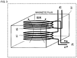
- Fig. 3 is a drawing showing the configuration of parts of the coils L1 and L2.
- the two coils, L1 and L2 are formed within a magnetic substrate 21 made of ferrite.
- the coils L1 and L2 have an identical coil axis and are aligned in the direction of the coil axis.
- the coils L1 and L2 are magnetically coupled.
- a port #1 is connected to the antenna resonant circuit AR, and a second port #2 is connected to the wireless IC.
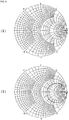
- Fig. 4(A) is a Smith chart showing the impedance (S11 of S parameter) in the case where the two coils, L1 and L2, are seen from the two transmission terminals, TX1 and TX2, of the wireless IC 11 shown in Fig. 2 .
- Fig. 4(A) is characteristics in the case where the coupling coefficient of the two coils, L1 and L2, shown in Fig. 2 is 0.9.
- Fig. 4(B) is characteristics in the case where the coupling coefficient is 0.00001.
- the impedance locus is significantly displaced from the right edge (infinite impedance) of the Smith chart clockwise, as shown in Fig. 4(B) .
- the frequency sweeps from 8.56 MHz to 18.56 MHz in the case where the two coils, L1 and L2 are coupled, the impedance locus is hardly displaced.
- the two coils are magnetically coupled in such a manner that the coils strengthen magnetic flux with each other. This doubles the amount of magnetic flux passing through each coil, doubling the equivalent inductance of each coil. This can halve the number of coil windings required to obtain necessary inductance, halving direct-current resistance. Halving of the number of coil windings allows downsizing of the device.
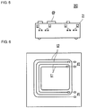
- Fig. 5 is a sectional view of the main part of a wireless IC device 202 according to a second embodiment.
- Fig. 6 is a drawing showing the configuration of two coils, L1 and L2, formed within the wireless IC device 202.
- the circuit configuration of the wireless IC device is similar to that according to the first embodiment shown in Fig. 2 .
- the two coils, L1 and L2 are formed in a spiral fashion.
- the first coil L1 is disposed inside the second coil L2 on approximately the same plane.
- a port #1 is connected to an antenna resonant circuit AR side, and a second port #2 is connected to a wireless IC side.
- the disposition of one coil, L1, inside the other coil, L2, as described above can strengthen the coupling between the two coils, L1 and L2, reliably matching impedances.
- the two coils, L1 and L2, shown in Fig. 5 are formed in approximately the same plane within the magnetic substrate 21 made of ferrite.
- Chip parts CP such as capacitors for impedance matching (C1, C2, and C3 shown in Fig. 2 ) and a capacitor CO for an antenna resonant circuit, are mounted on the upper surface of the magnetic substrate 21.
- the wireless IC 11, the control unit 12, the cipher processing unit 13, the clock circuit 14, and the like shown in Fig. 2 may be mounted on the upper surface of or within the magnetic substrate 21. This allows formation of a module (RFID module) including the wireless IC chip, facilitating incorporation into the wireless IC device.
- RFID module RFID module
- Fig. 7(A) is a circuit diagram of a wireless IC device 203A according to a third embodiment.
- Fig. 7(B) is a circuit diagram of another wireless IC device, 203B, according to the third embodiment.
- the wireless IC device 203A includes an antenna resonant circuit AR, a wireless IC 11, a control unit 12, a cipher processing unit 13, a clock circuit 14, and a characteristic stabilization circuit SM for matching impedances between the wireless IC 11 and the antenna resonant circuit AR.
- the characteristic stabilization circuit SM has a configuration different from that according to the first embodiment shown in Fig. 2 . Another difference is that the wireless IC 11 includes receiving terminals RX1 and RX2, which are balanced inputs.
- Both end portions of a first coil L11 are connected to the two receiving terminals, RX1 and RX2, of the wireless IC 11. Both end portions of a second coil L12 are connected to both end portions of a capacitor C3. The first coil L11 and the second coil L12 are magnetically coupled to each other.
- the two coils according to the present invention are applied to the balanced input terminals RX1 and RX2 of the wireless IC 11.
- Impedance elements Z1 and Z2 for impedance matching are connected between transmitting terminals TX1 and TX2 of the wireless IC 11 and both end portions of the capacitor C3.
- the two impedance elements, Z1 and Z2, are, for example, inductors (coils).
- the present invention is applicable not only to transmission signals, which are propagated between the wireless IC 11 and the antenna resonant circuit AR, but also to reception signals.
- the two coils, L11 and L12 are connected in parallel with the balanced signal lines propagated between the balanced input terminals RX1 and RX2 and the antenna resonant circuit AR.
- the two coils (L11 and L12) according to the present invention may be connected in parallel with the balanced signal lines propagated between the wireless IC and the antenna resonant circuit AR.
- the parallel connection of the two coils can eliminate the influence of static electricity from the antenna resonant circuit, preventing electrostatic breakdown of the wireless IC.
- Fig. 7(B) is an example configuration where reception signals are inputted into unbalanced terminals.
- a terminal RX is a reception signal input terminal
- a terminal GND is a ground terminal.
- the other configuration is the same as what is shown in Fig. 7(A) .
- the coil according to the present invention may be applied to the unbalanced reception signal terminals.
- Fig. 8 is a circuit diagram of a wireless IC device 204 according to a fourth embodiment.
- a characteristic stabilization circuit SM which matches impedances between two transmitting terminals (balanced output terminals), TX1 and TX2, of a wireless IC 11 and an antenna resonant circuit AR, includes two coils, L1 and L2.
- an impedance matching circuit between two receiving terminals (balanced input terminals), RX1 and RX2, of the wireless IC 11 and the antenna resonant circuit AR includes two coils, L3 and L4.
- the antenna resonant circuit AR in order to ground the neutral point (zero volt line) of balanced signals that are propagated between the antenna resonant circuit AR and the wireless IC 11, the antenna resonant circuit AR includes a series circuit of two capacitors, CO1 and CO2, having the same capacitance, and the connection point between the capacitors CO1 and CO2 and the center of the antenna coil AL are grounded.
- the impedance matching circuit also includes a series of capacitors C31 and C32, and the connection point between these capacitors is grounded.
- the stabilization of the potential of the neutral point as described above can suppress the deviation from zero volt of balanced signals within the wireless IC 11, stabilizing the operation.
- the circuit including the antenna resonant circuit includes the characteristic stabilization circuit
- a circuit including a high-frequency circuit for inputting or outputting balanced signals and a resonant circuit may include the characteristic stabilization circuit. That is, the characteristic stabilization circuit may be provided between the high-frequency circuit and the resonant circuit.
- impedances can be matched between the resonant circuit and the high-frequency circuit. This eliminates the need for a circuit for adjusting the resonant frequency of the resonant circuit, such as a trimmer capacitor, as well as the need for resonant-frequency adjustment work.
- the circuit including the wireless IC includes the characteristic stabilization circuit
- the characteristic stabilization circuit may be provided between a circuit for inputting or outputting balanced signals and a transmission line. This allows halving of the number of coil windings, halving direct-current resistance as well as downsizing the apparatus.
- the signal processing circuit includes the two coils that are magnetically coupled to each other, allowing signals at the two terminals to become approximately 180° out of phase with each other.
- a 1 st embodiment provides a signal processing circuit connected to a high-frequency circuit including two terminals, comprising two coils that are connected to the two terminals of the high-frequency circuit and are magnetically coupled to each other.
- a 2 nd embodiment provides the signal processing circuit according to the 1 st embodiment, wherein the two coils make signals at the two terminals approximately 180° out of phase with each other.
- a 3 rd embodiment provides the signal processing circuit according to any one of the to the 1 st and 2 nd embodiments, wherein the two terminals are balanced terminals that output or receive balanced signals, and wherein the two coils are connected in series with the balanced terminals of the high-frequency circuit, respectively.
- a 4 th embodiment provides the signal processing circuit according to any one of the to the 1 st and 2 nd embodiments, wherein the two terminals are balanced terminals that output or receive balanced signals, and the two coils comprise a first coil connected to the balanced terminal of the high-frequency circuit and a second coil magnetically coupled to the first coil.
- a 5 th embodiment provides the signal processing circuit according to any one of the 1 st to 4 th embodiments, wherein the two coils are magnetically coupled to each other in such a manner that the coils strengthen magnetic flux with each other.
- a 6 th embodiment provides the signal processing circuit according to any one of the 1 st to 5 th embodiments, wherein the two coils have an identical coil axis and are aligned in the direction of the coil axis.
- a 7 th embodiment provides the signal processing circuit according to any one of the 1 st to 5 th embodiments, wherein the two coils are formed on a plane, and one of the two coils is disposed inside the other coil.
- An 8 th embodiment provides the signal processing circuit according to any one of the 1 st to 7 th embodiments, wherein the two coils have an identical inductance.
- a 9 th embodiment provides the signal processing circuit according to any one of the 1 st to 8 th embodiments, wherein the two coils are formed on a multilayer substrate comprising a magnetic substance.
- a 10 th embodiment provides the signal processing circuit according to the 9 th embodiment, wherein at least part of a circuit electrically connected to the two coils is disposed on or within the multilayer substrate.
- An 11 th embodiment provides an antenna apparatus comprising the signal processing circuit according to any one of the 1 st to 10 th embodiments, wherein the high-frequency circuit is a wireless IC for use in a wireless IC device for communicating with an external device wirelessly, and the signal processing circuit is a part of an impedance matching circuit connected between an antenna resonant circuit and the balanced terminals, the antenna resonant circuit comprising an antenna coil for transmitting or receiving signals to or from the external device wirelessly.
Landscapes
- Engineering & Computer Science (AREA)
- Artificial Intelligence (AREA)
- Computer Vision & Pattern Recognition (AREA)
- Physics & Mathematics (AREA)
- General Physics & Mathematics (AREA)
- Theoretical Computer Science (AREA)
- Computer Networks & Wireless Communication (AREA)
- Signal Processing (AREA)
- Near-Field Transmission Systems (AREA)
- Details Of Aerials (AREA)
Abstract
Description
- The present invention relates to a signal processing circuit for use in a wireless IC device for performing noncontact communications using, for example, near-electromagnetic field, such as an RFID, and an antenna apparatus.
- NPL 1 discloses a reader for a noncontact IC card used as an RFID.
-
Fig. 1 shows an equivalent circuit of the reader for a noncontact IC card disclosed inNPL 1. This noncontact IC card is a reader that communicates with noncontact IC cards in a noncontact manner. An antenna resonant circuit AR composed of an antenna coil AL, equivalent resistors R11 and R12 corresponding to the Q value of the antenna coil, and a capacitor CO is formed in a manner corresponding to awireless IC 11. - Capacitors C1 and C2 and inductors L1 and L2 are provided in order to match impedances between the
wireless IC 11 and the antenna resonant circuit AR. A diode bridge DB is provided as a detector circuit, and capacitors C31, C32, C41, and C42 are provided as a smoothing circuit. - Adjustment of the capacitor CO within the antenna resonant circuit AR allows adjustment of the resonant frequency of the antenna resonant circuit AR, ensuring a favorable communication state.
- NPL 1: Hiroshi Karibe, "Extremely Understandable Book on Noncontact IC Card (provisional English title)," Nikkan Kogyo Shimbun Publishing, 2008/04/20, page 89.
- However, in such an wireless IC device for performing noncontact communications using near-electromagnetic field, variations in the inductance of the antenna coil or in the capacitance of the capacitor change the resonant frequency of the antenna resonant circuit. Further, depending on the ambient environment of the apparatus in which the wireless IC device (in particular, the antenna coil) is incorporated, the resonant frequency of the antenna resonant circuit deviates from the specified value. For this reason, there has been a need to form the capacitor CO shown in
Fig. 1 using a trimmer capacitor so as to adjust the resonant frequency of the antenna resonant circuit to the specified value for each device. - For example, in the case where this wireless IC device is used in mobile phone terminals, an antenna apparatus or wireless IC device must be prepared for each of extremely diverse devices. In the case where adjustment work is required for each apparatus, work man-hours are unfavorably required, resulting in an increase in cost.
- Further, the balanced terminals of the
wireless IC 11 require the inductors L1 and L2, respectively. Furthermore, the two inductors, L1 and L2, are required to have both a low direct-current resistance and a high direct-current superimposition characteristic (the allowable value of the direct current). This prevents downsizing of the device. For example, a current of several hundred mA or more passes through the inductors L1 and L2. For this reason, the inductors L1 and L2 are formed using coils much larger than other parts, preventing downsizing of the device. - The above-mentioned problems apply to apparatuses including an wireless IC, as well as apparatuses including a high-frequency circuit having balanced terminals. The same goes for apparatuses including an antenna resonant circuit, as well as apparatuses including a high-frequency circuit having balanced terminals and a resonant circuit.
- Accordingly, an object of the present invention is to provide a signal processing circuit and an antenna apparatus that do not need a circuit for adjusting the resonant frequency of a resonant circuit or resonant-frequency adjustment work and that are downsized.
- A signal processing circuit according to the present invention is a signal processing circuit connected to a high-frequency circuit including two terminals and is characterized in that it includes two coils that are connected to the two terminals of the high-frequency circuit and are magnetically coupled to each other.
- The two coils make signals at the two terminals, for example, approximately 180° out of phase with each other.
- The two terminals are, for example, balanced terminals that output or receive balanced signals. The two coils are connected in series with the balanced terminals of the high-frequency circuit, respectively.
- The two terminals are, for example, balanced terminals that output or receive balanced signals. The two coils include a first coil connected to the balanced terminal of the high-frequency circuit and a second coil magnetically coupled to the first coil. For example, the two coils are magnetically coupled to each other in such a manner that the coils strengthen magnetic flux with each other.
- If the two coils have an identical coil axis and are aligned in the direction of the coil axis, the two coils can be reliably magnetically coupled to each other.
- If the two coils are formed on a plane and one of the two coils is disposed inside the other coil, the two coils can be coupled with a high degree of coupling.
- The two coils preferably have an identical inductance. Thus, the advantage obtained by the coupling between the two coils is maximized, obtaining a high gain in a wider frequency band.
- If the two coils are formed, for example, on a multilayer substrate including a magnetic substance, the two coils having a predetermined inductance can further be downsized. Further, if at least part of a circuit electrically connected to the two coils is disposed on or within the multilayer substrate, the entire apparatus can be downsized and slimmed.
- An antenna apparatus according to the present invention is characterized in that it is configured as follows. The high-frequency circuit is a wireless IC for use in a wireless IC device for communicating with an external device wirelessly. The signal processing circuit is a part of an impedance matching circuit connected between an antenna resonant circuit and the balanced terminals, the antenna resonant circuit including an antenna coil for transmitting or receiving signals to or from the external device wirelessly.
- Since the two coils keep signals at the balanced terminals of the high-frequency circuit approximately 180° out of phase with each other over a wide frequency band, a high gain can be obtained over the wide frequency band.
- Further, even when the resonant frequency of the antenna resonant circuit itself deviates from the specified value somewhat, impedances can be matched between the antenna resonant circuit and the wireless IC. This eliminates the need for a circuit for adjusting the resonant frequency of the antenna resonant circuit, such as a trimmer capacitor, as well as the need for resonant-frequency adjustment work.
-
- [
Fig. 1] Fig. 1 is an equivalent circuit of a reader for use in a noncontact IC card disclosed inNPL 1. - [
Fig. 2] Fig. 2(A) is a circuit diagram of awireless IC device 201A according to a first embodiment.Fig. 2(B) is a circuit diagram of another wireless IC device, 201B, according to the first embodiment. - [
Fig. 3] Fig. 3 is a drawing showing the configuration of two coils, L1 and L2, included in the wireless IC device 201 according to the first embodiment. - [
Fig. 4] Fig. 4 includes Smith charts showing the impedance (S11 of S parameter) in the case where the two coils, L1 and L2, are seen from two transmission terminals, TX1 and TX2, shown inFig. 2 .Fig. 4(A) is characteristics in the case where the coupling coefficient of the two coils, L1 and L2, shown inFig. 2 is 0.9.Fig. 4(B) is characteristics in the case where the coupling coefficient is 0.00001. - [
Fig. 5] Fig. 5 is a sectional view of the main part of awireless IC device 202 according to a second embodiment. - [
Fig. 6] Fig. 6 is a drawing showing the configuration of two coils, L1 and L2, formed within thewireless IC device 202 according to the second embodiment. - [
Fig. 7] Fig. 7(A) is a circuit diagram of awireless IC device 203A according to a third embodiment.Fig. 7(B) is a circuit diagram of another wireless IC device, 203B, according to the third embodiment. - [
Fig. 8] Fig. 8 is a circuit diagram of awireless IC device 204 according to a fourth embodiment. Description of Embodiments -
Fig. 2(A) is a circuit diagram of awireless IC device 201A according to a first embodiment.Fig. 2(B) is a circuit diagram of another wireless IC device, 201B, according to the first embodiment. - First,
Fig. 2(A) will be described. As shown inFig. 2(A) , an antenna coil AL and a capacitor CO form an antenna resonant circuit AR. - The
wireless IC device 201A includes the antenna resonant circuit AR, awireless IC 11, acontrol unit 12, acipher processing unit 13, and aclock circuit 14. A characteristic stabilization circuit SM for impedance matching is provided between the antenna resonant circuit AR and thewireless IC 11. The characteristic stabilization circuit SM corresponds to a "signal processing circuit" according to the present invention. Specifically, a series circuit of capacitors C1, C2, and C3 is connected in parallel with the antenna resonant circuit AR. A first coil L1 is connected between a first transmitting terminal TX1 of thewireless IC 11 and the connection point between the capacitors C1 and C3. A second coil L2 is connected between a second transmitting terminal TX2 of thewireless IC 11 and the connection point between the capacitors C2 and C3. - The first coil L1 and the second coil L2 have an identical inductance. The first coil L1 and the second coil L2 are magnetically coupled in such a manner that the coils strengthen magnetic flux with each other. An impedance element Z1 is connected between a receiving terminal RX of the
wireless IC 11 and the connection point between the capacitors C1 and C3. The impedance element Z1 is, for example, a capacitor. - The first coil L1, the second coil L2, and the three capacitors, C1, C2, and C3, match impedances between the two transmitting terminals, TX1 and TX2, of the
wireless IC 11 and the antenna resonant circuit AR. - The capacitors C1, C2, and C3 and the impedance element Z1 match impedances between the receiving terminal RX of the
wireless IC 11 and the antenna resonant circuit AR. - The
wireless IC 11 outputs square wave signals of 13.56 MHz from the balanced transmitting terminals TX1 and TX2. The square wave signals drive the antenna resonant circuit AR via the two coils, L1 and L2, and the three capacitors, C1, C2, and C3 so that a magnetic field of 13.56 MHz is emitted from the antenna coil AL. If an RFID tag is adjacent to the antenna coil AL, the RFID tag receives the magnetic field signal and thus receives power, as well as changes the impedance of its internal wireless IC on the basis of its own ID so as to change the impedance of its antenna resonant circuit (ASK modulation). Thus, the RFID returns its ID by reflection of energy. - The
wireless IC 11 receives a signal generated by the ASK modulation and returned by the reflection and decrypts the ID. In the case where thewireless IC 11 transmits data or a command, it ASK modulates a drive voltage (current) of 13.56 MHz. The RFID tag receives the data or command from thewireless IC 11 by decrypting a variation in strength of a received carrier wave. - The
control unit 12 receives or outputs various types of data or commands for control from or to thewireless IC 11. Theclock circuit 14 provides clock signals to thewireless IC 11. Thecipher processing unit 13 performs a process with respect to a cipher to be used by the RFID. -
Fig. 2(B) is an example configuration where transmission signals are outputted from unbalanced terminals. InFig. 2(B) , a terminal TX is a transmission signal output terminal, and a terminal GND is a ground terminal. The other configuration is the same as what is shown inFig. 2(A) . As seen, the transmission signal output terminals of thewireless IC 11 may be unbalanced terminals. -
Fig. 3 is a drawing showing the configuration of parts of the coils L1 and L2. The two coils, L1 and L2, are formed within amagnetic substrate 21 made of ferrite. The coils L1 and L2 have an identical coil axis and are aligned in the direction of the coil axis. The coils L1 and L2 are magnetically coupled. - In
Fig. 3 , aport # 1 is connected to the antenna resonant circuit AR, and asecond port # 2 is connected to the wireless IC. -
Fig. 4(A) is a Smith chart showing the impedance (S11 of S parameter) in the case where the two coils, L1 and L2, are seen from the two transmission terminals, TX1 and TX2, of thewireless IC 11 shown inFig. 2 . -
Fig. 4(A) is characteristics in the case where the coupling coefficient of the two coils, L1 and L2, shown inFig. 2 is 0.9.Fig. 4(B) is characteristics in the case where the coupling coefficient is 0.00001. When the frequency sweeps from 8.56 MHz to 18.56 MHz in the case where the coupling coefficient between the two coils, L1 and L2, is approximately zero, the impedance locus is significantly displaced from the right edge (infinite impedance) of the Smith chart clockwise, as shown inFig. 4(B) . In contrast, when the frequency sweeps from 8.56 MHz to 18.56 MHz in the case where the two coils, L1 and L2, are coupled, the impedance locus is hardly displaced. This is because the coupling between the coils L1 and L2 keeps signals at the two transmission terminals, TX1 and TX2, of thewireless IC 11 approximately 180° out of phase with each other. That is, it is understood that balance characteristics can be obtained in the frequency band of 8.56 MHz to 18.56 MHz. Thus, impedances are reliably matched between the antenna resonant circuit AR and thewireless IC 11 over the wide frequency band, suppressing a reduction in gain due to the deviation of the resonant frequency of the antenna resonant circuit AR. This eliminates the need for a circuit for adjusting the resonant frequency of the antenna resonant circuit, such as a trimmer capacitor, as well as the need for resonant-frequency adjustment work. This eliminates the need for work such as adjustment of the resonant frequency of the antenna resonant circuit to a specified value for each device, for example, regardless of the ambient environment of the apparatus in which the wireless IC device (in particular, antenna coil) is incorporated. - Further, the two coils are magnetically coupled in such a manner that the coils strengthen magnetic flux with each other. This doubles the amount of magnetic flux passing through each coil, doubling the equivalent inductance of each coil. This can halve the number of coil windings required to obtain necessary inductance, halving direct-current resistance. Halving of the number of coil windings allows downsizing of the device.
- In contrast, if the two coils are magnetically coupled in such a manner that the coils weaken magnetic flux with each other, currents pass through the coils in the opposite directions. Thus, signals can easily be made approximately 180° out of phase with each other without having to design the inductance value.
-
Fig. 5 is a sectional view of the main part of awireless IC device 202 according to a second embodiment.Fig. 6 is a drawing showing the configuration of two coils, L1 and L2, formed within thewireless IC device 202. The circuit configuration of the wireless IC device is similar to that according to the first embodiment shown inFig. 2 . - In the example shown in
Fig. 6 , the two coils, L1 and L2, are formed in a spiral fashion. The first coil L1 is disposed inside the second coil L2 on approximately the same plane. Aport # 1 is connected to an antenna resonant circuit AR side, and asecond port # 2 is connected to a wireless IC side. The disposition of one coil, L1, inside the other coil, L2, as described above can strengthen the coupling between the two coils, L1 and L2, reliably matching impedances. - As shown in
Fig. 5 , the two coils, L1 and L2, shown inFig. 5 are formed in approximately the same plane within themagnetic substrate 21 made of ferrite. Chip parts CP, such as capacitors for impedance matching (C1, C2, and C3 shown inFig. 2 ) and a capacitor CO for an antenna resonant circuit, are mounted on the upper surface of themagnetic substrate 21. - The
wireless IC 11, thecontrol unit 12, thecipher processing unit 13, theclock circuit 14, and the like shown inFig. 2 may be mounted on the upper surface of or within themagnetic substrate 21. This allows formation of a module (RFID module) including the wireless IC chip, facilitating incorporation into the wireless IC device. -
Fig. 7(A) is a circuit diagram of awireless IC device 203A according to a third embodiment.Fig. 7(B) is a circuit diagram of another wireless IC device, 203B, according to the third embodiment. - First,
Fig. 7(A) will be described. As shown inFig. 7(A) , thewireless IC device 203A includes an antenna resonant circuit AR, awireless IC 11, acontrol unit 12, acipher processing unit 13, aclock circuit 14, and a characteristic stabilization circuit SM for matching impedances between thewireless IC 11 and the antenna resonant circuit AR. The characteristic stabilization circuit SM has a configuration different from that according to the first embodiment shown inFig. 2 . Another difference is that thewireless IC 11 includes receiving terminals RX1 and RX2, which are balanced inputs. - Both end portions of a first coil L11 are connected to the two receiving terminals, RX1 and RX2, of the
wireless IC 11. Both end portions of a second coil L12 are connected to both end portions of a capacitor C3. The first coil L11 and the second coil L12 are magnetically coupled to each other. - In the third embodiment, "the two coils" according to the present invention are applied to the balanced input terminals RX1 and RX2 of the
wireless IC 11. - Impedance elements Z1 and Z2 for impedance matching are connected between transmitting terminals TX1 and TX2 of the
wireless IC 11 and both end portions of the capacitor C3. The two impedance elements, Z1 and Z2, are, for example, inductors (coils). As seen, the present invention is applicable not only to transmission signals, which are propagated between thewireless IC 11 and the antenna resonant circuit AR, but also to reception signals. - Further, in the example shown in
Fig. 7(A) , the two coils, L11 and L12, are connected in parallel with the balanced signal lines propagated between the balanced input terminals RX1 and RX2 and the antenna resonant circuit AR. - As seen, the two coils (L11 and L12) according to the present invention may be connected in parallel with the balanced signal lines propagated between the wireless IC and the antenna resonant circuit AR.
- The parallel connection of the two coils can eliminate the influence of static electricity from the antenna resonant circuit, preventing electrostatic breakdown of the wireless IC.
-
Fig. 7(B) is an example configuration where reception signals are inputted into unbalanced terminals. InFig. 7(B) , a terminal RX is a reception signal input terminal, and a terminal GND is a ground terminal. The other configuration is the same as what is shown inFig. 7(A) . As seen, the coil according to the present invention may be applied to the unbalanced reception signal terminals. -
Fig. 8 is a circuit diagram of awireless IC device 204 according to a fourth embodiment. In the example shown inFig. 8 , a characteristic stabilization circuit SM, which matches impedances between two transmitting terminals (balanced output terminals), TX1 and TX2, of awireless IC 11 and an antenna resonant circuit AR, includes two coils, L1 and L2. Similarly, an impedance matching circuit between two receiving terminals (balanced input terminals), RX1 and RX2, of thewireless IC 11 and the antenna resonant circuit AR includes two coils, L3 and L4. - Further, in the example shown in
Fig. 8 , in order to ground the neutral point (zero volt line) of balanced signals that are propagated between the antenna resonant circuit AR and thewireless IC 11, the antenna resonant circuit AR includes a series circuit of two capacitors, CO1 and CO2, having the same capacitance, and the connection point between the capacitors CO1 and CO2 and the center of the antenna coil AL are grounded. The impedance matching circuit also includes a series of capacitors C31 and C32, and the connection point between these capacitors is grounded. - The stabilization of the potential of the neutral point as described above can suppress the deviation from zero volt of balanced signals within the
wireless IC 11, stabilizing the operation. - While, in the above-mentioned embodiments, the circuit including the antenna resonant circuit includes the characteristic stabilization circuit, a circuit including a high-frequency circuit for inputting or outputting balanced signals and a resonant circuit may include the characteristic stabilization circuit. That is, the characteristic stabilization circuit may be provided between the high-frequency circuit and the resonant circuit. Thus, even when the resonant frequency of the resonant circuit deviates from the specified value somewhat, impedances can be matched between the resonant circuit and the high-frequency circuit. This eliminates the need for a circuit for adjusting the resonant frequency of the resonant circuit, such as a trimmer capacitor, as well as the need for resonant-frequency adjustment work.
- While, in the above-mentioned embodiments, the circuit including the wireless IC includes the characteristic stabilization circuit, the characteristic stabilization circuit may be provided between a circuit for inputting or outputting balanced signals and a transmission line. This allows halving of the number of coil windings, halving direct-current resistance as well as downsizing the apparatus.
- Particularly, in circuits including an antenna resonant circuit that emits magnetic fields, coils are connected to two terminals that receives or outputs signals with a frequency lower than the resonant frequency of an antenna resonant circuit. Accordingly, signals at the two terminals readily become, for example, 120° or 160° out of phase with each other. On the other hand, the signal processing circuit according to the present invention includes the two coils that are magnetically coupled to each other, allowing signals at the two terminals to become approximately 180° out of phase with each other.
- Further embodiments are now described.
- A 1st embodiment provides a signal processing circuit connected to a high-frequency circuit including two terminals, comprising
two coils that are connected to the two terminals of the high-frequency circuit and are magnetically coupled to each other. - A 2nd embodiment provides the signal processing circuit according to the 1st embodiment, wherein the two coils make signals at the two terminals approximately 180° out of phase with each other.
- A 3rd embodiment provides the signal processing circuit according to any one of the to the 1st and 2nd embodiments, wherein the two terminals are balanced terminals that output or receive balanced signals, and wherein the two coils are connected in series with the balanced terminals of the high-frequency circuit, respectively.
- A 4th embodiment provides the signal processing circuit according to any one of the to the 1st and 2nd embodiments, wherein the two terminals are balanced terminals that output or receive balanced signals, and the two coils comprise a first coil connected to the balanced terminal of the high-frequency circuit and a second coil magnetically coupled to the first coil.
- A 5th embodiment provides the signal processing circuit according to any one of the 1st to 4th embodiments, wherein the two coils are magnetically coupled to each other in such a manner that the coils strengthen magnetic flux with each other.
- A 6th embodiment provides the signal processing circuit according to any one of the 1st to 5th embodiments, wherein the two coils have an identical coil axis and are aligned in the direction of the coil axis.
- A 7th embodiment provides the signal processing circuit according to any one of the 1st to 5th embodiments, wherein the two coils are formed on a plane, and one of the two coils is disposed inside the other coil.
- An 8th embodiment provides the signal processing circuit according to any one of the 1st to 7th embodiments, wherein the two coils have an identical inductance.
- A 9th embodiment provides the signal processing circuit according to any one of the 1st to 8th embodiments, wherein the two coils are formed on a multilayer substrate comprising a magnetic substance.
- A 10th embodiment provides the signal processing circuit according to the 9th embodiment, wherein at least part of a circuit electrically connected to the two coils is disposed on or within the multilayer substrate.
- An 11th embodiment provides an antenna apparatus comprising
the signal processing circuit according to any one of the 1st to 10th embodiments, wherein
the high-frequency circuit is a wireless IC for use in a wireless IC device for communicating with an external device wirelessly, and
the signal processing circuit is a part of an impedance matching circuit connected between an antenna resonant circuit and the balanced terminals, the antenna resonant circuit comprising an antenna coil for transmitting or receiving signals to or from the external device wirelessly. -
- 11 wireless IC
- 12 control unit
- 13 cipher processing unit
- 14 clock circuit
- 21 magnetic substrate
- 201A, 201B, 203A, 203B, 204B wireless IC device
- AL antenna coil
- AR antenna resonant circuit
- CO1, CO2 capacitor
- C1, C2, C3 capacitor
- CO capacitor
- CP chip part
- DB diode bridge
- L1 first coil
- L2 second coil
- L11, L12 coil
- L3, L4 coil
- Q antenna coil
- RX, RX1, RX2 receiving terminal
- SM characteristic stabilization circuit
- TX, TX1, TX2 transmitting terminal
- Z1, Z2 impedance element
Claims (4)
- An antenna apparatus, comprising:a wireless IC (11) configured to be used in a wireless IC device (203B) to perform wireless communicating with external equipment or an external device, the wireless IC (11) including a first terminal (RX) and a second terminal (GND), andan antenna resonant circuit (AR) configured to transmit and receive a signal by the wireless communicating with the external equipment, one end of the antenna resonance circuit (AR) being connected to ground;a first coil (L11) connected between the first terminal (RX) of the wireless IC (11) and the second terminal (GND) of the wireless IC (11); anda second coil (L12) connected between a first end of the antenna resonant circuit (AR) and ground;wherein the first and second coils (L11, L12) are magnetically coupled to each other.
- The antenna apparatus according to Claim 1, wherein the first and second coils (L11, L12) are formed within a magnetic substrate (21).
- The antenna apparatus according to Claim 2, wherein the magnetic substrate (21) is made of ferrite.
- The antenna apparatus according to any one of Claims 1 to 3, wherein the first and second coils (L11, L12) have an identical coil axis and are aligned in the direction of the coil axis.
Applications Claiming Priority (3)
| Application Number | Priority Date | Filing Date | Title |
|---|---|---|---|
| JP2009060429 | 2009-03-13 | ||
| PCT/JP2010/054247 WO2010104179A1 (en) | 2009-03-13 | 2010-03-12 | Signal processing circuit and antenna apparatus |
| EP10750930.9A EP2408063B1 (en) | 2009-03-13 | 2010-03-12 | Antenna apparatus |
Related Parent Applications (2)
| Application Number | Title | Priority Date | Filing Date |
|---|---|---|---|
| EP10750930.9A Division-Into EP2408063B1 (en) | 2009-03-13 | 2010-03-12 | Antenna apparatus |
| EP10750930.9A Division EP2408063B1 (en) | 2009-03-13 | 2010-03-12 | Antenna apparatus |
Publications (2)
| Publication Number | Publication Date |
|---|---|
| EP3276746A1 true EP3276746A1 (en) | 2018-01-31 |
| EP3276746B1 EP3276746B1 (en) | 2019-05-22 |
Family
ID=42728464
Family Applications (2)
| Application Number | Title | Priority Date | Filing Date |
|---|---|---|---|
| EP17190125.9A Active EP3276746B1 (en) | 2009-03-13 | 2010-03-12 | Antenna apparatus |
| EP10750930.9A Not-in-force EP2408063B1 (en) | 2009-03-13 | 2010-03-12 | Antenna apparatus |
Family Applications After (1)
| Application Number | Title | Priority Date | Filing Date |
|---|---|---|---|
| EP10750930.9A Not-in-force EP2408063B1 (en) | 2009-03-13 | 2010-03-12 | Antenna apparatus |
Country Status (5)
| Country | Link |
|---|---|
| US (1) | US8912906B2 (en) |
| EP (2) | EP3276746B1 (en) |
| JP (2) | JP5316638B2 (en) |
| CN (1) | CN102341956B (en) |
| WO (1) | WO2010104179A1 (en) |
Families Citing this family (38)
| Publication number | Priority date | Publication date | Assignee | Title |
|---|---|---|---|---|
| EP2251934B1 (en) | 2008-03-03 | 2018-05-02 | Murata Manufacturing Co. Ltd. | Wireless ic device and wireless communication system |
| CN103295056B (en) | 2008-05-21 | 2016-12-28 | 株式会社村田制作所 | Wireless IC device |
| CN104077622B (en) | 2008-05-26 | 2016-07-06 | 株式会社村田制作所 | The authenticating method of wireless IC device system and Wireless IC device |
| DE112009002384B4 (en) | 2008-11-17 | 2021-05-06 | Murata Manufacturing Co., Ltd. | Antenna and wireless IC component |
| JP5510450B2 (en) | 2009-04-14 | 2014-06-04 | 株式会社村田製作所 | Wireless IC device |
| EP2424041B1 (en) | 2009-04-21 | 2018-11-21 | Murata Manufacturing Co., Ltd. | Antenna apparatus and resonant frequency setting method of same |
| CN102577646B (en) | 2009-09-30 | 2015-03-04 | 株式会社村田制作所 | Circuit substrate and method of manufacture thereof |
| JP5304580B2 (en) | 2009-10-02 | 2013-10-02 | 株式会社村田製作所 | Wireless IC device |
| JP5327334B2 (en) | 2009-11-04 | 2013-10-30 | 株式会社村田製作所 | Communication terminal and information processing system |
| JP5652470B2 (en) | 2010-03-03 | 2015-01-14 | 株式会社村田製作所 | Wireless communication module and wireless communication device |
| CN102668241B (en) | 2010-03-24 | 2015-01-28 | 株式会社村田制作所 | RFID system |
| JP5630499B2 (en) | 2010-03-31 | 2014-11-26 | 株式会社村田製作所 | Antenna apparatus and wireless communication device |
| JP2011238016A (en) * | 2010-05-10 | 2011-11-24 | Sony Corp | Non-contact communication medium, antenna pattern arrangement medium, communication device and antenna adjustment method |
| GB2495418B (en) * | 2010-07-28 | 2017-05-24 | Murata Manufacturing Co | Antenna apparatus and communication terminal instrument |
| CN104899639B (en) | 2011-02-28 | 2018-08-07 | 株式会社村田制作所 | Wireless communication devices |
| JP5630566B2 (en) | 2011-03-08 | 2014-11-26 | 株式会社村田製作所 | Antenna device and communication terminal device |
| WO2012141070A1 (en) | 2011-04-13 | 2012-10-18 | 株式会社村田製作所 | Wireless ic device and wireless communication terminal |
| WO2012157596A1 (en) | 2011-05-16 | 2012-11-22 | 株式会社村田製作所 | Wireless ic device |
| JP5333707B2 (en) | 2011-07-15 | 2013-11-06 | 株式会社村田製作所 | Wireless communication device |
| WO2013011865A1 (en) | 2011-07-19 | 2013-01-24 | 株式会社村田製作所 | Antenna module, antenna device, rfid tag, and communication terminal device |
| JP5418737B2 (en) | 2011-09-09 | 2014-02-19 | 株式会社村田製作所 | Antenna apparatus and wireless device |
| CN103380432B (en) | 2011-12-01 | 2016-10-19 | 株式会社村田制作所 | Wireless IC device and manufacturing method thereof |
| JP5354137B1 (en) | 2012-01-30 | 2013-11-27 | 株式会社村田製作所 | Wireless IC device |
| WO2013125610A1 (en) | 2012-02-24 | 2013-08-29 | 株式会社村田製作所 | Antenna device and wireless communication device |
| TWI613686B (en) | 2012-03-23 | 2018-02-01 | Lg伊諾特股份有限公司 | Method of manufacturing a wireless power receiver |
| JP6313744B2 (en) | 2012-03-23 | 2018-04-18 | エルジー イノテック カンパニー リミテッド | Wireless power receiver |
| WO2013153697A1 (en) | 2012-04-13 | 2013-10-17 | 株式会社村田製作所 | Rfid tag inspection method, and inspection device |
| GB2519247B (en) * | 2012-06-28 | 2017-11-29 | Murata Manufacturing Co | Antenna device, feed element, and communication terminal device |
| DE202013012361U1 (en) * | 2012-08-28 | 2016-06-20 | Murata Manufacturing Co., Ltd. | Antenna device and communication terminal |
| KR102155199B1 (en) | 2013-12-23 | 2020-09-11 | 삼성전자주식회사 | Matching circuit, NFC device and electronic system including the same |
| WO2018183296A1 (en) * | 2017-03-28 | 2018-10-04 | Sri International | Authentication apparatus, system and methods using unclonable identifiers |
| US11580344B2 (en) | 2015-01-09 | 2023-02-14 | Sri International | Authentication apparatus, system and methods using unclonable identifiers |
| ITUB20153500A1 (en) | 2015-09-09 | 2017-03-09 | St Microelectronics Srl | PROCEDURE FOR TRANSMITTING POWER AND DATA THROUGH A GALVANIC INSULATION BARRIER, CORRESPONDENT SYSTEM AND EQUIPMENT |
| ITUB20156047A1 (en) * | 2015-12-01 | 2017-06-01 | St Microelectronics Srl | GALVANIC INSULATION SYSTEM, EQUIPMENT AND PROCEDURE |
| US9948193B2 (en) | 2016-06-10 | 2018-04-17 | Stmicroelectronics S.R.L. | Galvanically isolated DC-DC converter with bidirectional data transmission |
| IT201600088207A1 (en) | 2016-08-30 | 2018-03-02 | St Microelectronics Srl | GALVANIC INSULATION CIRCUIT, CORRESPONDENT SYSTEM AND PROCEDURE |
| EP3764557A4 (en) * | 2018-03-09 | 2021-05-05 | Toray Industries, Inc. | WIRELESS COMMUNICATION DEVICE |
| CN114389055B (en) * | 2022-01-18 | 2024-07-05 | 安徽安努奇科技有限公司 | Antenna assembly and communication system |
Citations (3)
| Publication number | Priority date | Publication date | Assignee | Title |
|---|---|---|---|---|
| US20050125093A1 (en) * | 2003-10-01 | 2005-06-09 | Sony Corporation | Relaying apparatus and communication system |
| US20050242900A1 (en) * | 2002-03-15 | 2005-11-03 | Hiroyuki Nakamura | Balanced high-frequency filter, antenna duplexer, balanced high-frequency circuit and communication apparatus |
| EP1976056A1 (en) * | 2006-01-19 | 2008-10-01 | Murata Manufacturing Co. Ltd. | Radio ic device and radio ic device part |
Family Cites Families (12)
| Publication number | Priority date | Publication date | Assignee | Title |
|---|---|---|---|---|
| KR100686991B1 (en) * | 2000-03-08 | 2007-02-27 | 마쯔시다덴기산교 가부시키가이샤 | Electronic equipment using noise filter and noise filter |
| WO2001093422A1 (en) * | 2000-06-01 | 2001-12-06 | Koninklijke Philips Electronics N.V. | Rf circuit |
| JP2001358514A (en) | 2000-06-14 | 2001-12-26 | Sony Corp | Wireless terminal |
| DE60215382T2 (en) * | 2001-11-02 | 2007-08-23 | Avid Identification Systems, Inc., Norco | DOUBLE ANTENNA COIL TRANSPONDER SYSTEM |
| WO2004114240A2 (en) * | 2003-06-13 | 2004-12-29 | Xtec, Incorporated | Differential radio frequency identification reader |
| JP2005244848A (en) | 2004-02-27 | 2005-09-08 | Sony Corp | Balun filter |
| SE0402945D0 (en) * | 2004-11-30 | 2004-11-30 | Abb Research Ltd | Industrial robot |
| JP4312188B2 (en) * | 2005-09-30 | 2009-08-12 | Tdk株式会社 | Inductor element |
| JP2007274026A (en) * | 2006-03-30 | 2007-10-18 | Tdk Corp | Noise filter |
| JP4803253B2 (en) * | 2006-04-26 | 2011-10-26 | 株式会社村田製作所 | Article with power supply circuit board |
| WO2008149946A1 (en) * | 2007-06-08 | 2008-12-11 | Murata Manufacturing Co., Ltd. | Wireless ic device |
| JP3148168U (en) * | 2008-10-21 | 2009-02-05 | 株式会社村田製作所 | Wireless IC device |
-
2010
- 2010-03-12 JP JP2011503881A patent/JP5316638B2/en not_active Expired - Fee Related
- 2010-03-12 WO PCT/JP2010/054247 patent/WO2010104179A1/en not_active Ceased
- 2010-03-12 CN CN201080011719.5A patent/CN102341956B/en not_active Expired - Fee Related
- 2010-03-12 EP EP17190125.9A patent/EP3276746B1/en active Active
- 2010-03-12 EP EP10750930.9A patent/EP2408063B1/en not_active Not-in-force
-
2011
- 2011-09-12 US US13/229,814 patent/US8912906B2/en active Active
-
2013
- 2013-07-04 JP JP2013140956A patent/JP2013242887A/en active Pending
Patent Citations (3)
| Publication number | Priority date | Publication date | Assignee | Title |
|---|---|---|---|---|
| US20050242900A1 (en) * | 2002-03-15 | 2005-11-03 | Hiroyuki Nakamura | Balanced high-frequency filter, antenna duplexer, balanced high-frequency circuit and communication apparatus |
| US20050125093A1 (en) * | 2003-10-01 | 2005-06-09 | Sony Corporation | Relaying apparatus and communication system |
| EP1976056A1 (en) * | 2006-01-19 | 2008-10-01 | Murata Manufacturing Co. Ltd. | Radio ic device and radio ic device part |
Non-Patent Citations (1)
| Title |
|---|
| HIROSHI KARIBE: "Extremely Understandable Book on Noncontact IC Card (provisional English title", 20 April 2008, NIKKAN KOGYO SHIMBUN PUBLISHING, pages: 89 |
Also Published As
| Publication number | Publication date |
|---|---|
| EP2408063B1 (en) | 2018-04-18 |
| EP2408063A4 (en) | 2017-03-22 |
| JPWO2010104179A1 (en) | 2012-09-13 |
| US8912906B2 (en) | 2014-12-16 |
| US20120001701A1 (en) | 2012-01-05 |
| EP2408063A1 (en) | 2012-01-18 |
| JP5316638B2 (en) | 2013-10-16 |
| WO2010104179A1 (en) | 2010-09-16 |
| JP2013242887A (en) | 2013-12-05 |
| CN102341956B (en) | 2015-03-11 |
| EP3276746B1 (en) | 2019-05-22 |
| CN102341956A (en) | 2012-02-01 |
Similar Documents
| Publication | Publication Date | Title |
|---|---|---|
| EP2408063B1 (en) | Antenna apparatus | |
| EP2266076B1 (en) | Transceiving circuit for contactless communication and nfc device or rfid reader/writer device comprising such a transceiving circuit | |
| EP3379734B1 (en) | Nfc reader with remote antenna | |
| EP2213011B1 (en) | Transceiving circuit for contactless communication | |
| EP1865445B1 (en) | Wireless communication terminal apparatus and method of controlling same | |
| CN110061750B (en) | Method for controlling tuning of communication frequency of antenna and corresponding system | |
| JP5761251B2 (en) | Antenna device and communication device | |
| JP5218369B2 (en) | RFID and wireless communication device | |
| US11699056B2 (en) | RFID inlay | |
| US9893751B2 (en) | Antenna circuit, communication device, and communication method for improving reception signal quality | |
| US9626614B2 (en) | Protection of a radio frequency transmit-receive terminal against electromagnetic disturbances | |
| US20170179998A1 (en) | Front end circuit and communication apparatus | |
| JP2008506177A (en) | Signal processing circuit for a communication partner device for contactless communication | |
| WO2021059565A1 (en) | Rfid inlay |
Legal Events
| Date | Code | Title | Description |
|---|---|---|---|
| PUAI | Public reference made under article 153(3) epc to a published international application that has entered the european phase |
Free format text: ORIGINAL CODE: 0009012 |
|
| STAA | Information on the status of an ep patent application or granted ep patent |
Free format text: STATUS: THE APPLICATION HAS BEEN PUBLISHED |
|
| AC | Divisional application: reference to earlier application |
Ref document number: 2408063 Country of ref document: EP Kind code of ref document: P |
|
| AK | Designated contracting states |
Kind code of ref document: A1 Designated state(s): AT BE BG CH CY CZ DE DK EE ES FI FR GB GR HR HU IE IS IT LI LT LU LV MC MK MT NL NO PL PT RO SE SI SK SM TR |
|
| STAA | Information on the status of an ep patent application or granted ep patent |
Free format text: STATUS: REQUEST FOR EXAMINATION WAS MADE |
|
| 17P | Request for examination filed |
Effective date: 20180731 |
|
| RBV | Designated contracting states (corrected) |
Designated state(s): AT BE BG CH CY CZ DE DK EE ES FI FR GB GR HR HU IE IS IT LI LT LU LV MC MK MT NL NO PL PT RO SE SI SK SM TR |
|
| GRAP | Despatch of communication of intention to grant a patent |
Free format text: ORIGINAL CODE: EPIDOSNIGR1 |
|
| STAA | Information on the status of an ep patent application or granted ep patent |
Free format text: STATUS: GRANT OF PATENT IS INTENDED |
|
| RIC1 | Information provided on ipc code assigned before grant |
Ipc: H01Q 1/50 20060101AFI20181025BHEP Ipc: H01Q 7/00 20060101ALI20181025BHEP Ipc: H01Q 11/08 20060101ALI20181025BHEP Ipc: H01Q 9/27 20060101ALI20181025BHEP Ipc: H04B 5/00 20060101ALI20181025BHEP Ipc: G06K 7/00 20060101ALI20181025BHEP Ipc: G06K 17/00 20060101ALI20181025BHEP Ipc: H04B 5/02 20060101ALI20181025BHEP |
|
| INTG | Intention to grant announced |
Effective date: 20181203 |
|
| GRAS | Grant fee paid |
Free format text: ORIGINAL CODE: EPIDOSNIGR3 |
|
| GRAA | (expected) grant |
Free format text: ORIGINAL CODE: 0009210 |
|
| STAA | Information on the status of an ep patent application or granted ep patent |
Free format text: STATUS: THE PATENT HAS BEEN GRANTED |
|
| AC | Divisional application: reference to earlier application |
Ref document number: 2408063 Country of ref document: EP Kind code of ref document: P |
|
| AK | Designated contracting states |
Kind code of ref document: B1 Designated state(s): AT BE BG CH CY CZ DE DK EE ES FI FR GB GR HR HU IE IS IT LI LT LU LV MC MK MT NL NO PL PT RO SE SI SK SM TR |
|
| REG | Reference to a national code |
Ref country code: GB Ref legal event code: FG4D |
|
| REG | Reference to a national code |
Ref country code: CH Ref legal event code: EP |
|
| REG | Reference to a national code |
Ref country code: IE Ref legal event code: FG4D |
|
| REG | Reference to a national code |
Ref country code: DE Ref legal event code: R096 Ref document number: 602010059141 Country of ref document: DE |
|
| REG | Reference to a national code |
Ref country code: AT Ref legal event code: REF Ref document number: 1137223 Country of ref document: AT Kind code of ref document: T Effective date: 20190615 |
|
| REG | Reference to a national code |
Ref country code: NL Ref legal event code: MP Effective date: 20190522 |
|
| REG | Reference to a national code |
Ref country code: LT Ref legal event code: MG4D |
|
| PG25 | Lapsed in a contracting state [announced via postgrant information from national office to epo] |
Ref country code: SE Free format text: LAPSE BECAUSE OF FAILURE TO SUBMIT A TRANSLATION OF THE DESCRIPTION OR TO PAY THE FEE WITHIN THE PRESCRIBED TIME-LIMIT Effective date: 20190522 Ref country code: HR Free format text: LAPSE BECAUSE OF FAILURE TO SUBMIT A TRANSLATION OF THE DESCRIPTION OR TO PAY THE FEE WITHIN THE PRESCRIBED TIME-LIMIT Effective date: 20190522 Ref country code: NO Free format text: LAPSE BECAUSE OF FAILURE TO SUBMIT A TRANSLATION OF THE DESCRIPTION OR TO PAY THE FEE WITHIN THE PRESCRIBED TIME-LIMIT Effective date: 20190822 Ref country code: PT Free format text: LAPSE BECAUSE OF FAILURE TO SUBMIT A TRANSLATION OF THE DESCRIPTION OR TO PAY THE FEE WITHIN THE PRESCRIBED TIME-LIMIT Effective date: 20190922 Ref country code: FI Free format text: LAPSE BECAUSE OF FAILURE TO SUBMIT A TRANSLATION OF THE DESCRIPTION OR TO PAY THE FEE WITHIN THE PRESCRIBED TIME-LIMIT Effective date: 20190522 Ref country code: LT Free format text: LAPSE BECAUSE OF FAILURE TO SUBMIT A TRANSLATION OF THE DESCRIPTION OR TO PAY THE FEE WITHIN THE PRESCRIBED TIME-LIMIT Effective date: 20190522 Ref country code: ES Free format text: LAPSE BECAUSE OF FAILURE TO SUBMIT A TRANSLATION OF THE DESCRIPTION OR TO PAY THE FEE WITHIN THE PRESCRIBED TIME-LIMIT Effective date: 20190522 Ref country code: NL Free format text: LAPSE BECAUSE OF FAILURE TO SUBMIT A TRANSLATION OF THE DESCRIPTION OR TO PAY THE FEE WITHIN THE PRESCRIBED TIME-LIMIT Effective date: 20190522 |
|
| PG25 | Lapsed in a contracting state [announced via postgrant information from national office to epo] |
Ref country code: BG Free format text: LAPSE BECAUSE OF FAILURE TO SUBMIT A TRANSLATION OF THE DESCRIPTION OR TO PAY THE FEE WITHIN THE PRESCRIBED TIME-LIMIT Effective date: 20190822 Ref country code: LV Free format text: LAPSE BECAUSE OF FAILURE TO SUBMIT A TRANSLATION OF THE DESCRIPTION OR TO PAY THE FEE WITHIN THE PRESCRIBED TIME-LIMIT Effective date: 20190522 Ref country code: GR Free format text: LAPSE BECAUSE OF FAILURE TO SUBMIT A TRANSLATION OF THE DESCRIPTION OR TO PAY THE FEE WITHIN THE PRESCRIBED TIME-LIMIT Effective date: 20190823 |
|
| REG | Reference to a national code |
Ref country code: AT Ref legal event code: MK05 Ref document number: 1137223 Country of ref document: AT Kind code of ref document: T Effective date: 20190522 |
|
| PG25 | Lapsed in a contracting state [announced via postgrant information from national office to epo] |
Ref country code: DK Free format text: LAPSE BECAUSE OF FAILURE TO SUBMIT A TRANSLATION OF THE DESCRIPTION OR TO PAY THE FEE WITHIN THE PRESCRIBED TIME-LIMIT Effective date: 20190522 Ref country code: AT Free format text: LAPSE BECAUSE OF FAILURE TO SUBMIT A TRANSLATION OF THE DESCRIPTION OR TO PAY THE FEE WITHIN THE PRESCRIBED TIME-LIMIT Effective date: 20190522 Ref country code: EE Free format text: LAPSE BECAUSE OF FAILURE TO SUBMIT A TRANSLATION OF THE DESCRIPTION OR TO PAY THE FEE WITHIN THE PRESCRIBED TIME-LIMIT Effective date: 20190522 Ref country code: CZ Free format text: LAPSE BECAUSE OF FAILURE TO SUBMIT A TRANSLATION OF THE DESCRIPTION OR TO PAY THE FEE WITHIN THE PRESCRIBED TIME-LIMIT Effective date: 20190522 Ref country code: RO Free format text: LAPSE BECAUSE OF FAILURE TO SUBMIT A TRANSLATION OF THE DESCRIPTION OR TO PAY THE FEE WITHIN THE PRESCRIBED TIME-LIMIT Effective date: 20190522 Ref country code: SK Free format text: LAPSE BECAUSE OF FAILURE TO SUBMIT A TRANSLATION OF THE DESCRIPTION OR TO PAY THE FEE WITHIN THE PRESCRIBED TIME-LIMIT Effective date: 20190522 |
|
| REG | Reference to a national code |
Ref country code: DE Ref legal event code: R097 Ref document number: 602010059141 Country of ref document: DE |
|
| PG25 | Lapsed in a contracting state [announced via postgrant information from national office to epo] |
Ref country code: SM Free format text: LAPSE BECAUSE OF FAILURE TO SUBMIT A TRANSLATION OF THE DESCRIPTION OR TO PAY THE FEE WITHIN THE PRESCRIBED TIME-LIMIT Effective date: 20190522 Ref country code: IT Free format text: LAPSE BECAUSE OF FAILURE TO SUBMIT A TRANSLATION OF THE DESCRIPTION OR TO PAY THE FEE WITHIN THE PRESCRIBED TIME-LIMIT Effective date: 20190522 |
|
| PLBE | No opposition filed within time limit |
Free format text: ORIGINAL CODE: 0009261 |
|
| STAA | Information on the status of an ep patent application or granted ep patent |
Free format text: STATUS: NO OPPOSITION FILED WITHIN TIME LIMIT |
|
| PG25 | Lapsed in a contracting state [announced via postgrant information from national office to epo] |
Ref country code: TR Free format text: LAPSE BECAUSE OF FAILURE TO SUBMIT A TRANSLATION OF THE DESCRIPTION OR TO PAY THE FEE WITHIN THE PRESCRIBED TIME-LIMIT Effective date: 20190522 |
|
| 26N | No opposition filed |
Effective date: 20200225 |
|
| PG25 | Lapsed in a contracting state [announced via postgrant information from national office to epo] |
Ref country code: PL Free format text: LAPSE BECAUSE OF FAILURE TO SUBMIT A TRANSLATION OF THE DESCRIPTION OR TO PAY THE FEE WITHIN THE PRESCRIBED TIME-LIMIT Effective date: 20190522 |
|
| PG25 | Lapsed in a contracting state [announced via postgrant information from national office to epo] |
Ref country code: SI Free format text: LAPSE BECAUSE OF FAILURE TO SUBMIT A TRANSLATION OF THE DESCRIPTION OR TO PAY THE FEE WITHIN THE PRESCRIBED TIME-LIMIT Effective date: 20190522 |
|
| PG25 | Lapsed in a contracting state [announced via postgrant information from national office to epo] |
Ref country code: MC Free format text: LAPSE BECAUSE OF FAILURE TO SUBMIT A TRANSLATION OF THE DESCRIPTION OR TO PAY THE FEE WITHIN THE PRESCRIBED TIME-LIMIT Effective date: 20190522 |
|
| REG | Reference to a national code |
Ref country code: CH Ref legal event code: PL |
|
| REG | Reference to a national code |
Ref country code: BE Ref legal event code: MM Effective date: 20200331 |
|
| PG25 | Lapsed in a contracting state [announced via postgrant information from national office to epo] |
Ref country code: LU Free format text: LAPSE BECAUSE OF NON-PAYMENT OF DUE FEES Effective date: 20200312 |
|
| PG25 | Lapsed in a contracting state [announced via postgrant information from national office to epo] |
Ref country code: CH Free format text: LAPSE BECAUSE OF NON-PAYMENT OF DUE FEES Effective date: 20200331 Ref country code: IE Free format text: LAPSE BECAUSE OF NON-PAYMENT OF DUE FEES Effective date: 20200312 Ref country code: LI Free format text: LAPSE BECAUSE OF NON-PAYMENT OF DUE FEES Effective date: 20200331 Ref country code: FR Free format text: LAPSE BECAUSE OF NON-PAYMENT OF DUE FEES Effective date: 20200331 |
|
| PG25 | Lapsed in a contracting state [announced via postgrant information from national office to epo] |
Ref country code: BE Free format text: LAPSE BECAUSE OF NON-PAYMENT OF DUE FEES Effective date: 20200331 |
|
| GBPC | Gb: european patent ceased through non-payment of renewal fee |
Effective date: 20200312 |
|
| PG25 | Lapsed in a contracting state [announced via postgrant information from national office to epo] |
Ref country code: GB Free format text: LAPSE BECAUSE OF NON-PAYMENT OF DUE FEES Effective date: 20200312 |
|
| PGFP | Annual fee paid to national office [announced via postgrant information from national office to epo] |
Ref country code: DE Payment date: 20220322 Year of fee payment: 13 |
|
| PG25 | Lapsed in a contracting state [announced via postgrant information from national office to epo] |
Ref country code: MT Free format text: LAPSE BECAUSE OF FAILURE TO SUBMIT A TRANSLATION OF THE DESCRIPTION OR TO PAY THE FEE WITHIN THE PRESCRIBED TIME-LIMIT Effective date: 20190522 Ref country code: CY Free format text: LAPSE BECAUSE OF FAILURE TO SUBMIT A TRANSLATION OF THE DESCRIPTION OR TO PAY THE FEE WITHIN THE PRESCRIBED TIME-LIMIT Effective date: 20190522 |
|
| PG25 | Lapsed in a contracting state [announced via postgrant information from national office to epo] |
Ref country code: MK Free format text: LAPSE BECAUSE OF FAILURE TO SUBMIT A TRANSLATION OF THE DESCRIPTION OR TO PAY THE FEE WITHIN THE PRESCRIBED TIME-LIMIT Effective date: 20190522 Ref country code: IS Free format text: LAPSE BECAUSE OF FAILURE TO SUBMIT A TRANSLATION OF THE DESCRIPTION OR TO PAY THE FEE WITHIN THE PRESCRIBED TIME-LIMIT Effective date: 20190922 |
|
| REG | Reference to a national code |
Ref country code: DE Ref legal event code: R119 Ref document number: 602010059141 Country of ref document: DE |
|
| PG25 | Lapsed in a contracting state [announced via postgrant information from national office to epo] |
Ref country code: DE Free format text: LAPSE BECAUSE OF NON-PAYMENT OF DUE FEES Effective date: 20231003 |