EP3276603A1 - Method and apparatus for controlling liquid crystal display - Google Patents
Method and apparatus for controlling liquid crystal display Download PDFInfo
- Publication number
- EP3276603A1 EP3276603A1 EP17181308.2A EP17181308A EP3276603A1 EP 3276603 A1 EP3276603 A1 EP 3276603A1 EP 17181308 A EP17181308 A EP 17181308A EP 3276603 A1 EP3276603 A1 EP 3276603A1
- Authority
- EP
- European Patent Office
- Prior art keywords
- display frame
- time
- lcd
- display
- liquid crystal
- Prior art date
- Legal status (The legal status is an assumption and is not a legal conclusion. Google has not performed a legal analysis and makes no representation as to the accuracy of the status listed.)
- Withdrawn
Links
- 239000004973 liquid crystal related substance Substances 0.000 title claims abstract description 105
- 238000000034 method Methods 0.000 title claims abstract description 49
- 238000010586 diagram Methods 0.000 description 15
- 239000000758 substrate Substances 0.000 description 14
- 230000005540 biological transmission Effects 0.000 description 3
- 230000003044 adaptive effect Effects 0.000 description 2
- 239000003086 colorant Substances 0.000 description 2
- 230000000694 effects Effects 0.000 description 2
- 238000001914 filtration Methods 0.000 description 2
- 241001270131 Agaricus moelleri Species 0.000 description 1
- 230000006978 adaptation Effects 0.000 description 1
- 239000013078 crystal Substances 0.000 description 1
- 238000005192 partition Methods 0.000 description 1
- 238000002360 preparation method Methods 0.000 description 1
- 239000010409 thin film Substances 0.000 description 1
- 238000002834 transmittance Methods 0.000 description 1
Images

Classifications
-
- G—PHYSICS
- G09—EDUCATION; CRYPTOGRAPHY; DISPLAY; ADVERTISING; SEALS
- G09G—ARRANGEMENTS OR CIRCUITS FOR CONTROL OF INDICATING DEVICES USING STATIC MEANS TO PRESENT VARIABLE INFORMATION
- G09G3/00—Control arrangements or circuits, of interest only in connection with visual indicators other than cathode-ray tubes
- G09G3/20—Control arrangements or circuits, of interest only in connection with visual indicators other than cathode-ray tubes for presentation of an assembly of a number of characters, e.g. a page, by composing the assembly by combination of individual elements arranged in a matrix no fixed position being assigned to or needed to be assigned to the individual characters or partial characters
- G09G3/34—Control arrangements or circuits, of interest only in connection with visual indicators other than cathode-ray tubes for presentation of an assembly of a number of characters, e.g. a page, by composing the assembly by combination of individual elements arranged in a matrix no fixed position being assigned to or needed to be assigned to the individual characters or partial characters by control of light from an independent source
- G09G3/36—Control arrangements or circuits, of interest only in connection with visual indicators other than cathode-ray tubes for presentation of an assembly of a number of characters, e.g. a page, by composing the assembly by combination of individual elements arranged in a matrix no fixed position being assigned to or needed to be assigned to the individual characters or partial characters by control of light from an independent source using liquid crystals
- G09G3/3611—Control of matrices with row and column drivers
- G09G3/3618—Control of matrices with row and column drivers with automatic refresh of the display panel using sense/write circuits
-
- G—PHYSICS
- G09—EDUCATION; CRYPTOGRAPHY; DISPLAY; ADVERTISING; SEALS
- G09G—ARRANGEMENTS OR CIRCUITS FOR CONTROL OF INDICATING DEVICES USING STATIC MEANS TO PRESENT VARIABLE INFORMATION
- G09G3/00—Control arrangements or circuits, of interest only in connection with visual indicators other than cathode-ray tubes
- G09G3/20—Control arrangements or circuits, of interest only in connection with visual indicators other than cathode-ray tubes for presentation of an assembly of a number of characters, e.g. a page, by composing the assembly by combination of individual elements arranged in a matrix no fixed position being assigned to or needed to be assigned to the individual characters or partial characters
- G09G3/34—Control arrangements or circuits, of interest only in connection with visual indicators other than cathode-ray tubes for presentation of an assembly of a number of characters, e.g. a page, by composing the assembly by combination of individual elements arranged in a matrix no fixed position being assigned to or needed to be assigned to the individual characters or partial characters by control of light from an independent source
- G09G3/3406—Control of illumination source
-
- G—PHYSICS
- G09—EDUCATION; CRYPTOGRAPHY; DISPLAY; ADVERTISING; SEALS
- G09G—ARRANGEMENTS OR CIRCUITS FOR CONTROL OF INDICATING DEVICES USING STATIC MEANS TO PRESENT VARIABLE INFORMATION
- G09G3/00—Control arrangements or circuits, of interest only in connection with visual indicators other than cathode-ray tubes
- G09G3/20—Control arrangements or circuits, of interest only in connection with visual indicators other than cathode-ray tubes for presentation of an assembly of a number of characters, e.g. a page, by composing the assembly by combination of individual elements arranged in a matrix no fixed position being assigned to or needed to be assigned to the individual characters or partial characters
- G09G3/2007—Display of intermediate tones
- G09G3/2074—Display of intermediate tones using sub-pixels
-
- G—PHYSICS
- G09—EDUCATION; CRYPTOGRAPHY; DISPLAY; ADVERTISING; SEALS
- G09G—ARRANGEMENTS OR CIRCUITS FOR CONTROL OF INDICATING DEVICES USING STATIC MEANS TO PRESENT VARIABLE INFORMATION
- G09G3/00—Control arrangements or circuits, of interest only in connection with visual indicators other than cathode-ray tubes
- G09G3/20—Control arrangements or circuits, of interest only in connection with visual indicators other than cathode-ray tubes for presentation of an assembly of a number of characters, e.g. a page, by composing the assembly by combination of individual elements arranged in a matrix no fixed position being assigned to or needed to be assigned to the individual characters or partial characters
- G09G3/34—Control arrangements or circuits, of interest only in connection with visual indicators other than cathode-ray tubes for presentation of an assembly of a number of characters, e.g. a page, by composing the assembly by combination of individual elements arranged in a matrix no fixed position being assigned to or needed to be assigned to the individual characters or partial characters by control of light from an independent source
- G09G3/36—Control arrangements or circuits, of interest only in connection with visual indicators other than cathode-ray tubes for presentation of an assembly of a number of characters, e.g. a page, by composing the assembly by combination of individual elements arranged in a matrix no fixed position being assigned to or needed to be assigned to the individual characters or partial characters by control of light from an independent source using liquid crystals
- G09G3/3611—Control of matrices with row and column drivers
- G09G3/3648—Control of matrices with row and column drivers using an active matrix
-
- G—PHYSICS
- G09—EDUCATION; CRYPTOGRAPHY; DISPLAY; ADVERTISING; SEALS
- G09G—ARRANGEMENTS OR CIRCUITS FOR CONTROL OF INDICATING DEVICES USING STATIC MEANS TO PRESENT VARIABLE INFORMATION
- G09G2300/00—Aspects of the constitution of display devices
- G09G2300/04—Structural and physical details of display devices
- G09G2300/0439—Pixel structures
- G09G2300/0452—Details of colour pixel setup, e.g. pixel composed of a red, a blue and two green components
-
- G—PHYSICS
- G09—EDUCATION; CRYPTOGRAPHY; DISPLAY; ADVERTISING; SEALS
- G09G—ARRANGEMENTS OR CIRCUITS FOR CONTROL OF INDICATING DEVICES USING STATIC MEANS TO PRESENT VARIABLE INFORMATION
- G09G2310/00—Command of the display device
- G09G2310/02—Addressing, scanning or driving the display screen or processing steps related thereto
- G09G2310/0237—Switching ON and OFF the backlight within one frame
-
- G—PHYSICS
- G09—EDUCATION; CRYPTOGRAPHY; DISPLAY; ADVERTISING; SEALS
- G09G—ARRANGEMENTS OR CIRCUITS FOR CONTROL OF INDICATING DEVICES USING STATIC MEANS TO PRESENT VARIABLE INFORMATION
- G09G2310/00—Command of the display device
- G09G2310/08—Details of timing specific for flat panels, other than clock recovery
-
- G—PHYSICS
- G09—EDUCATION; CRYPTOGRAPHY; DISPLAY; ADVERTISING; SEALS
- G09G—ARRANGEMENTS OR CIRCUITS FOR CONTROL OF INDICATING DEVICES USING STATIC MEANS TO PRESENT VARIABLE INFORMATION
- G09G2320/00—Control of display operating conditions
- G09G2320/02—Improving the quality of display appearance
- G09G2320/0252—Improving the response speed
-
- G—PHYSICS
- G09—EDUCATION; CRYPTOGRAPHY; DISPLAY; ADVERTISING; SEALS
- G09G—ARRANGEMENTS OR CIRCUITS FOR CONTROL OF INDICATING DEVICES USING STATIC MEANS TO PRESENT VARIABLE INFORMATION
- G09G2320/00—Control of display operating conditions
- G09G2320/02—Improving the quality of display appearance
- G09G2320/0257—Reduction of after-image effects
-
- G—PHYSICS
- G09—EDUCATION; CRYPTOGRAPHY; DISPLAY; ADVERTISING; SEALS
- G09G—ARRANGEMENTS OR CIRCUITS FOR CONTROL OF INDICATING DEVICES USING STATIC MEANS TO PRESENT VARIABLE INFORMATION
- G09G2320/00—Control of display operating conditions
- G09G2320/02—Improving the quality of display appearance
- G09G2320/0261—Improving the quality of display appearance in the context of movement of objects on the screen or movement of the observer relative to the screen
-
- G—PHYSICS
- G09—EDUCATION; CRYPTOGRAPHY; DISPLAY; ADVERTISING; SEALS
- G09G—ARRANGEMENTS OR CIRCUITS FOR CONTROL OF INDICATING DEVICES USING STATIC MEANS TO PRESENT VARIABLE INFORMATION
- G09G2320/00—Control of display operating conditions
- G09G2320/06—Adjustment of display parameters
- G09G2320/0613—The adjustment depending on the type of the information to be displayed
- G09G2320/062—Adjustment of illumination source parameters
-
- G—PHYSICS
- G09—EDUCATION; CRYPTOGRAPHY; DISPLAY; ADVERTISING; SEALS
- G09G—ARRANGEMENTS OR CIRCUITS FOR CONTROL OF INDICATING DEVICES USING STATIC MEANS TO PRESENT VARIABLE INFORMATION
- G09G2320/00—Control of display operating conditions
- G09G2320/06—Adjustment of display parameters
- G09G2320/0626—Adjustment of display parameters for control of overall brightness
- G09G2320/064—Adjustment of display parameters for control of overall brightness by time modulation of the brightness of the illumination source
-
- G—PHYSICS
- G09—EDUCATION; CRYPTOGRAPHY; DISPLAY; ADVERTISING; SEALS
- G09G—ARRANGEMENTS OR CIRCUITS FOR CONTROL OF INDICATING DEVICES USING STATIC MEANS TO PRESENT VARIABLE INFORMATION
- G09G2320/00—Control of display operating conditions
- G09G2320/08—Arrangements within a display terminal for setting, manually or automatically, display parameters of the display terminal
Definitions
- the present disclosure relates to the field of display technology, and more particularly, to a method and an apparatus for controlling a liquid crystal display.
- LCD Liquid crystal display
- VR Virtual Reality
- an LCD refreshes a display frame according to a predetermined frame rate (for example, 60 frames/second), the single frame display time of each display frame is about 16.7 milliseconds.
- the single frame display time may be divided into effective data refreshing time T1 and blanking time T2.
- a display driver integrated circuit DDIC
- the current display frame is displayed constantly, while a preparation for the refreshment of the next display frame is made.
- the liquid crystal may be flipped during a refreshment process, this kind of flipping will cause serious dynamic blur.
- the present disclosure provides a method and an apparatus for controlling a liquid crystal display.
- the technical solutions are as following.
- a method for controlling a liquid crystal display including: controlling a backlight circuit of the LCD to be in an unconnected state during effective data refreshing time of an i th display frame, in which the effective data refreshing time is a time period during which the i th display frame is scanned line by line, where i represents a positive integer; and controlling the backlight circuit to be in a connected state during blanking time of the i th display frame, in which the blanking time is a time period during which a current display frame is displayed constantly.
- controlling a backlight circuit of the liquid crystal display LCD to be in an unconnected state during effective data refreshing time of an i th display frame includes providing a pause-width modulation signal to the backlight circuit of the LCD, in which a wave pattern of the pause-width modulation signal corresponding to the effective data refreshing time of the i th display frame is a first level signal, and the first level signal is used for controlling the backlight circuit of the LCD to be in the unconnected state.
- a wave pattern of the pause-width modulation signal corresponding to the blanking time of the i th display frame is a second level signal, and the second level signal is used for controlling the backlight circuit of the LCD to be in the connected state.
- the method further includes refreshing display data of the i th display frame into the LCD during the effective data refreshing time of the i th display frame, in which a duration of the effective data refreshing time is shorter than a predetermined duration.
- refreshing display data of the i th display frame into the LCD includes: acquiring the display data of the i th display frame from a central processing unit (CPU), in which an acquisition time of the display data is less than a first threshold, and refreshing the display data of the i th display frame line by line into each line of pixel units of the LCD in an order from top to bottom and left to right.
- CPU central processing unit
- a flipping response time of liquid crystal in each pixel unit of the LCD is less than a second threshold, and/or a capacitance value of a storage capacitance of each pixel unit of the LCD is bigger than a third threshold.
- an apparatus for controlling a liquid crystal display includes a first control module and a second control module.
- the first control module is configured to control a backlight circuit of the LCD to be in an unconnected state during effective data refreshing time of an i th display frame, in which the effective data refreshing time is a time period during which the i th display frame is scanned line by line, in which i represents a positive integer.
- the second control module is configured to control the backlight circuit to be in a connected state during blanking time of the i th display frame, in which the blanking time is a time period during which a current display frame is displayed constantly.
- the first control module is configured to provide a pause-width modulation signal to said backlight circuit of the LCD, in which a wave pattern of the pause-width modulation signal corresponding to the effective data refreshing time of the i th display frame is a first level signal, and the first level signal is configured to control the backlight circuit to be in the unconnected state.
- a wave pattern of the pause-width modulation signal corresponding to the blanking time of the i th display frame is a second level signal, and the second level signal is used for controlling the backlight circuit of the LCD to be in the connected state.
- a level value corresponding to the first level signal is lower than a level value corresponding to the second level signal.
- the apparatus further includes: a data refreshing module, which is configured to refresh display data of the i th display frame into the LCD during the effective data refreshing time of the i th display frame, in which a duration of the effective data refreshing time is shorter than a predetermined duration.
- a data refreshing module which is configured to refresh display data of the i th display frame into the LCD during the effective data refreshing time of the i th display frame, in which a duration of the effective data refreshing time is shorter than a predetermined duration.
- the data refreshing module further includes a data acquiring sub-module and a data refreshing sub-module.
- the data acquiring sub-module is configured to acquire the display data of the i th display frame from a CPU, in which an acquisition time of the display data is less than a first threshold.
- the data refreshing sub-module is configured to refresh the display data of the i th display frame line by line into each line of pixel units of the LCD in an order from top to bottom and left to right.
- a flipping response time of liquid crystal in each pixel unit of the LCD is less than a second threshold, and/or a capacitance value of a storage capacitance of each pixel unit of the LCD is bigger than a third threshold.
- an electronic device includes LCD and DDIC, in which, the DDIC is configured to control a backlight circuit of the LCD to be in an unconnected state during effective data refreshing time of an i th display frame, in which the effective data refreshing time is a time period during which the i th display frame is scanned line by line, where i represents a positive integer; and to control the backlight circuit to be in a connected state during blanking time of the i th display frame, in which the blanking time is a time period during which a current display frame is displayed constantly.
- a duration of the effective data refreshing time of the i th display frame is shorter than a predetermined duration.
- a flipping response time of liquid crystal in each pixel unit of the LCD is less than a second threshold, and/or a capacitance value of a storage capacitance of each pixel unit of the LCD is bigger than a third threshold.
- the backlight circuit of the LCD With controlling the backlight circuit of the LCD to be in an unconnected state during the effective data refreshing time of the i th display frame, in which the effective data refreshing time is the time period during which the i th display frame is scanned line by line, and i represents a positive integer, and controlling the backlight circuit of the LCD to be in a connected state during the blanking time of the i th display frame, the problems of the liquid crystal flipping during a refreshment process and the serious dynamic blur caused by this kind of flipping in the related art are solved.
- the backlight circuit is controlled to be in an unconnected state, i. e. the backlight is not illumined, thus making the flipping process of the liquid crystal invisible, a serious dynamic blur caused by liquid crystal flipping is avoided and the display performance of an LCD is optimized.
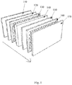
- Fig. 1 shows a structure of an LCD panel.
- the LCD panel includes a backlight circuit 110, a lower polarizer 120, an array substrate 130, a liquid crystal layer 140, an upper substrate 150, a color filter layer 160 and an upper polarizer 170.
- the lower polarizer 120 is located on top of the backlight circuit 110
- the array substrate 130 is located on top of the lower polarizer 120
- liquid crystal layer 140 is located on top of the array substrate 130
- the upper substrate 150 is located on top of the liquid crystal layer 140
- the color filter layer 160 is located on top of the upper substrate 150
- the upper polarizer 170 is located on top of the color filter layer 160.
- the backlight circuit 110 is adaptive for providing backlight for an LCD panel, the backlight circuit 110 could be, but not limited to, any of the following kinds: electro luminescent (EL), cold cathode fluorescent lamp (CCFL), light emitting diode (LDE) and etc..
- EL electro luminescent
- CCFL cold cathode fluorescent lamp
- LDE light emitting diode
- the lower polarizer 120 and the upper polarizer 170 are adaptive for transmission of a light ray in certain directions, and the transmission axis of the lower polarizer 120 and transmission axis of the upper polarizer 170 are perpendicular to each other.
- each pixel unit includes K sub pixel units, usually, each pixel unit includes 3 sub pixel units, which are a red (R) sub pixel unit, a green (G) sub pixel unit, and a blue (B) sub pixel unit.
- each pixel unit includes 4 sub pixel units, which are an R sub pixel unit, a G sub pixel unit, a B sub pixel unit, and a white (W) sub pixel unit. That is, the value of K may be 3 or 4.
- the liquid crystal molecules in the liquid crystal layer 140 may rotate under the control of a thin film transistor (TFT) area of the array substrate 130, with different rotate angles corresponding to different transmittance of light, thus forming the display gray scale of each pixel unit.
- TFT thin film transistor
- color filter layer 160 is stuck to the up-surface of the upper substrate 150, the color filter layer 160 makes it possible for the LCD panel to present a colorful picture
- color filter layer 160 includes R, G, B three different colors (red, green, blue) of light filtering areas arranged in array. There is a one to one correspondence between the light filtering areas and the sub pixel units on the array substrate 130.
- the light generated by the backlight circuit 110 may go through the lower polarizer 120, the array substrate 130, the liquid crystal layer 140, the upper substrate 150, the color filter layer 160 and the upper polarizer 170 in an order from bottom to top, the rotation direction of the liquid crystal molecules in the liquid crystal layer 140 may be controlled by the voltage provided by the array substrate 130, the luminance of the light may be changed according to the rotation direction of the liquid crystal molecules in the liquid crystal layer 140 thereby the sub pixel units corresponding to the different colors R, G, B in the color filter layer may come into different gray scales, thus realizing the display of data.
- Fig. 2 is a schematic diagram illustrating a structure of a liquid crystal driver circuit.
- the liquid crystal driver circuit includes a DDIC, m*n crystal units 1, m scan lines 21 and n data lines 31, in which, the DDIC includes scan driver chip 2 and data driver chip 3.
- the liquid crystal units 1 are arranged in an array of m rows and n columns.
- Each liquid crystal unit 1 includes a sub pixel electrode 11 and a TFT switch element.
- a TFT switch element includes a source electrode 12, a grid electrode 13 and a drain electrode 14.
- a sub pixel electrode 11 is connected to a source electrode 12 of a TFT switch element.
- a sub pixel electrode 11 may be a red sub pixel electrode R, a green sub pixel electrode G or a blue sub pixel electrode B.
- the scan driver chip 2 includes m scan pins and each scan pin is connected to a scan line 21.
- Each row of the liquid crystal units 1 corresponds to a scan line 21, and the scan line 21 is connected to the grid electrodes 13 of the liquid crystal units 1 in the corresponding row.
- the data driver chip 3 includes n data pins and each data pin is connected to a data line 31.
- Each column of the liquid crystal units 1 corresponds to a data line 31, and the data line 31 is connected to the drain electrodes 14 of the liquid crystal units 1 in the corresponding column.
- the scan driver chip 2 sends scan signals to the scan lines 21 line by line from top to bottom, thus a scan line 21 which receives a scan signal could set the corresponding row of liquid crystal units 1 to an operation state.
- the data driver chip 3 transmits a gray scale voltage of the pixel points corresponding to the line of the liquid crystal units 1 to the corresponding drain electrodes 14 through a data line 31, thus the data driver chip 3 may store the corresponding gray scale voltage into a sub pixel electrode 11, and make each and every sub pixel electrode 11 display the corresponding level of gray scale, thus realizing the display of a frame of data.
- the single frame display time is divided into effective data refresh time and blanking time
- the effective data refreshing time is the time period during which the i th display frame is scanned line by line
- the blanking time is the time period during which the current display frame is displayed.
- the DDIC output a pause-width modulation signal to the backlight circuit of the LCD
- the wave pattern of the pause-width modulation signal corresponding to the effective data refreshing time of the i th display frame is a first level signal
- the first level signal is used for controlling the backlight circuit of the LCD to be in an unconnected state, the backlight is not illumined.
- the DDIC output a pause-width modulation signal to the backlight circuit of the LCD
- the wave pattern of the pause-width modulation signal corresponding to the blanking time of the i th display frame is a second level signal
- the second level signal is used for controlling the backlight circuit of the LCD to be in a connected state, the backlight is illumined.
- single frame display time is divided into effective data refreshing time and blanking time, in which, the effective data refreshing time is relatively longer and blanking time is shorter. While in the embodiments of the present disclosure, in the same single frame display time, the effective data refreshing time is relatively shorter and blanking time is longer, thus the flipping time of the liquid crystal during a refreshment process is shorter, a serious dynamic blur caused by such flipping is avoided and the display performance of an LCD is optimized.
- Fig. 3 is a flow chart showing a method for controlling a liquid crystal display according to an example embodiment, as shown in Fig. 3 , the method for controlling liquid crystal display includes the following actions.
- the backlight circuit of the LCD is controlled to be in an unconnected state during the effective data refreshing time of the i th display frame.
- the effective data refreshing time is the time period during which the i th display frame is scanned line by line, in which i represents a positive integer.
- the backlight circuit in an unconnected state means the backlight is not illumined.
- the backlight circuit of the LCD is controlled to be in a connected state during the blanking time of the i th display frame.
- the blanking time is the time period during which the current display frame is displayed constantly.
- the backlight circuit in a connected state means the backlight is illumined.
- the method for controlling a liquid crystal display provided in the embodiments of the present disclosure, by controlling the backlight circuit of the LCD to be in an unconnected state during the effective data refreshing time of the i th display frame, in which the effective data refreshing time is the time period during which the i th display frame is scanned line by line, in which i represents a positive integer, and by controlling the backlight circuit of the LCD to be in a connected state during the blanking time of the i th display frame, the problems of the liquid crystal flipping during a refreshment process and the serious dynamic blur caused by this kind of flipping in the related art are solved.
- the backlight circuit is controlled to be in an unconnected state, i. e. the backlight is not illumined, thus making the flipping process of the liquid crystal invisible, a serious dynamic blur caused by liquid crystal flipping is avoided and the display performance of an LCD is optimized.
- Fig. 4 is a flow chart showing a method for controlling a liquid crystal display according to another example embodiment. As shown in Fig. 4 , the method for controlling liquid crystal display includes the followings.
- a pause-width modulation signal is provided to the backlight circuit of the LCD.
- the LCD refreshes the i th display frame according to a predetermined frame rate, for example, a predetermined frame rate of 60 frames/second, then the single frame display time of each display frame is about 16.7 milliseconds.
- the single frame display time is divided into effective data refresh time and blanking time.
- DDIC refreshes the display data of the i th display frame from the first line at the left top corner downwardly line by line.
- DDIC outputs a corresponding pause-width modulation signal according to the refreshing position of the i th display frame in the LCD and transmits the output pause-width modulation signal to the backlight circuit of the LCD.
- the i th display frame includes at least one kind of the following: one display frame for displaying data, parts of the display frames for displaying data and all the display frames for displaying data, in which i represents a positive integer.
- the backlight circuit of the LCD is controlled to be in an unconnected state when the wave pattern of the pause-width modulation signal corresponding to the effective data refreshing time of the i th display frame is a first level signal.
- the first level signal is configured to control the backlight circuit to be in an unconnected state.
- the backlight circuit receives a pause-width modulation signal transmitted by the DDIC in which the wave pattern corresponding to the effective data refreshing time of the i th display frame is the first level signal, the voltage of the backlight circuit is in low level, the backlight circuit is in an unconnected state, the backlight is not illumined, thus making the flipping process of the liquid crystal invisible, a serious dynamic blur caused by liquid crystal flipping is avoided and the display performance of an LCD is optimized.
- the effective data refreshing time is the time period during which the i th display frame is scanned line by line.
- the backlight circuit of the LCD is controlled to be in a connected state when the wave pattern of the pause-width modulation signal corresponding to the blanking time of the i th display frame is a second level signal.
- the second level signal is configured to control the backlight circuit to be in a connected state.
- the backlight circuit receives a pause-width modulation signal transmitted by the DDIC in which the wave pattern corresponding to the blanking time of the i th display frame is the second level signal, the voltage of the backlight circuit is in high level, the backlight circuit is in a connected state, the backlight is illumined, so as to display the refreshed display data of the i th display frame and optimize the display performance of the LCD.
- the blanking time is the time period during which the current display frame is displayed.
- the level value corresponding to the first level signal is lower than a level value corresponding to the second level signal.
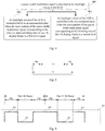
- the pause-width modulation signal 61 output from the DDIC to the backlight circuit is shown in Fig. 6 .
- the single frame display time of two display frames is illustrated, in which, the wave pattern corresponding to the effective data refreshing time T1 of the i th display frame is low level signal 62, the wave pattern corresponding to the blanking time vbp and vfp of the i th display frame is a high level signal 63, the wave pattern corresponding to the effective data refreshing time T1 of the i+1 th display frame is low level signal 62, the wave pattern corresponding to the blanking time vbp and vfp of the i+1 th display frame is high level signal 63.
- first level signal being a low level signal
- second level signal being a high level signal
- the method for controlling a liquid crystal display provided in the embodiments of the present disclosure, by controlling the backlight circuit of the LCD to be in an unconnected state during the effective data refreshing time of the i th display frame, in which the effective data refreshing time is the time period during which the i th display frame is scanned line by line, in which i represents a positive integer, and by controlling the backlight circuit of the LCD to be in a connected state during the blanking time of the i th display frame, the problems of the liquid crystal flipping during a refreshment process and the serious dynamic blur caused by this kind of flipping in the related art are solved.
- the backlight circuit is controlled to be in an unconnected state, i. e. the backlight is not illumined, thus making the flipping process of the liquid crystal invisible, a serious dynamic blur caused by liquid crystal flipping is avoided and the display performance of an LCD is optimized.
- the display data of the i th display frame is refreshed into the LCD during the effective data refreshing time of the i th display frame, the duration of the effective data refreshing time is shorter than a predetermined duration.
- the effective data refreshing time is the time period during which the i th display frame is scanned line by line.
- the LCD refreshes the i th display frame according to a predetermined frame rate, for example, a predetermined frame rate of 60 frames/second, then the single frame display time of each display frame is about 16.7 milliseconds.
- the single frame display time is divided into effective data refresh time and blanking time, i represents a positive integer.
- the display data of the i th display frame is refreshed into the LCD during the effective data refreshing time of the i th display frame, and the display data of the i th display frame is kept being displayed during the blanking time of the i th display frame.
- the duration of the effective data refreshing time is shorter than a predetermined duration.
- the present block may be substituted by the following sub steps, as shown in Fig. 8A .
- the display data of the i th display frame is acquired from a CPU, the acquisition time of acquiring the display data is less than a first threshold.
- the DDIC could acquire display data of the i th display frame from the CPU through the following two ways.
- the DDIC acquires display data of the i th display frame from the CPU during the effective data refreshing time of the i th display frame, so that the DDIC may refresh the acquired display data of the i th display frame.
- the acquisition time of acquiring by the DDIC the display data of the i th display frame from the CPU is less than a first threshold, for example, the acquisition time is 3 ms.
- the DDIC acquires display data of the i th display frame from the CPU during the blanking time of the i th display frame, so that the DDIC may refresh the acquired display data of the i th display frame when entering the effective data refreshing time of the i th display frame.
- the blanking time during which the DDIC acquires the display data of the i th display frame is shown in Fig. 5 as the area corresponding to vbp.
- the acquisition time of acquiring by the DDIC the display data of the i th display frame from the CPU is set to be less than a first threshold so that the duration of the effective data refreshing time of a display frame could be reduced and a serious dynamic blur caused by liquid crystal flipping could be avoided.
- the display data of the i th display frame is refreshed line by line into each line of the pixel units of the LCD in an order from top to bottom and left to right.
- the display data of the i th display frame is transmitted from the CPU to the DDIC, the display data of the i th display frame is refreshed line by line into each line of the pixel units of the LCD in an order from top to bottom and left to right.
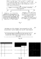
- the specific process of a line by line refreshment is shown in Fig. 8B, Fig 8 shows a line by line refreshment process of display data with 13lines.
- the data is refreshed in an order from top to bottom and left to right
- the left graph shows a schematic diagram showing that the DDIC starts to refresh the first line from the left top corner
- the middle graph shows a schematic diagram showing that the DDIC refreshes to the middle of the fourth line from the left top corner in the order from top to bottom and left to right
- the right graph shows a schematic diagram showing that the DDIC finishes refreshment of the whole 13th lines starting from the left top corner and in the order from top to bottom and left to right.
- the flipping response time of the liquid crystal in each and every pixel unit of the LCD is less than a second threshold.
- the speed of flipping is a physical characteristic of liquid crystal, in order to make the flipping response time of the liquid crystal be less than a second threshold, usually the liquid crystal with a relatively higher flipping speed is chosen.
- the flipping response time of the liquid crystal in each and every pixel unit of the LCD is set to be less than a second threshold so that the duration of the effective data refreshing time of a display frame could be reduced and a serious dynamic blur caused by liquid crystal flipping could be avoided.
- the flipping response time of the liquid crystal is 8 ms by using a kind of liquid crystal with a lower flipping speed, while by using a kind of liquid crystal with a higher flipping speed, the flipping response time of the liquid crystal is 5 ms.
- the refreshing velocity of the display data of the i th display frame is inversely proportional to the flipping response time of the liquid crystal, when the flipping response time of the liquid crystal is less than the second threshold, the refreshing velocity of the display data of the i th display frame is faster than a predetermined velocity.
- the duration of the effective data refreshing time of a display frame could be reduced and a serious dynamic blur caused by liquid crystal flipping could be avoided.
- the duration of the effective data refreshing time of the i th display frame is reduced, the blanking time of the i th display frame is increased correspondingly.
- a way of increasing the capacitance value of the storage capacitance may be used.
- the capacitance value of the storage capacitance of each and every pixel unit of the LCD is bigger than a third threshold.
- the storage capacitance of each and every pixel unit in the LCD is used to provide a power supply for keeping displaying the display data of the present display frame when the display data of the i th display frame is in the blanking time.
- the storage capacitance of each and every pixel unit in the LCD is located between the liquid crystal layer 140 and the array substrate 130 of the LCD panel shown in Fig. 1 (not shown in the figure).
- the duration of the effective data refreshing time of the i th display frame is shorter than a predetermined duration
- the duration of the blanking time of the i th display frame is longer than a predetermined duration.
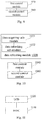
- Fig. 9 is a block diagram showing an apparatus for controlling a liquid crystal display according to an example embodiment, as shown in Fig. 9 , the apparatus for controlling a liquid crystal display includes, but is not limited to, a first control module 920, and a second control module 940.
- the first control module 920 is configured to control a backlight circuit of the LCD to be in an unconnected state during effective data refreshing time of an i th display frame, in which the effective data refreshing time is a time period during which the i th display frame is scanned line by line, in which i represents a positive integer.
- the second control module 940 is configured to control the backlight circuit to be in a connected state during blanking time of the i th display frame, in which the blanking time is a time period during which a current display frame is displayed constantly.
- the apparatus for controlling a liquid crystal display provided in the embodiments of the present disclosure, by controlling the backlight circuit of the LCD to be in an unconnected state during the effective data refreshing time of the i th display frame, in which the effective data refreshing time is the time period during which the i th display frame is scanned line by line, in which i represents a positive integer, and by controlling the backlight circuit of the LCD to be in a connected state during the blanking time of the i th display frame, the problems of the liquid crystal flipping during a refreshment process and the serious dynamic blur caused by this kind of flipping in the related art are solved.
- the backlight circuit is controlled to be in an unconnected state, i. e. the backlight is not illumined, thus making the flipping process of the liquid crystal invisible, a serious dynamic blur caused by liquid crystal flipping is avoided and the display performance of an LCD is optimized.
- Fig. 10 is a block diagram showing an apparatus for controlling a liquid crystal display according to another example embodiment, as shown in Fig. 10 , the apparatus for controlling liquid crystal display includes, but not limited to, a data refreshing module 1020, a first control module 1040, and a second control module 1060.
- the data refreshing module 1020 is configured to refresh the display data of the i th display frame into the LCD during the effective data refreshing time of the i th display frame, in which a duration of the effective data refreshing time is shorter than a predetermined duration.
- the data refreshing module 1020 includes a data acquiring sub-module 1021 and a data refreshing sub-module 1022.
- the data acquiring sub-module 1021 is configured to acquire the display data of the i th display frame from a CPU, in which an acquisition time of the display data is less than a first threshold.
- a flipping response time of liquid crystal in each and every pixel unit of the LCD is less than a second threshold, and/or a capacitance value of a storage capacitance of each and every pixel unit of the LCD is bigger than a third threshold.
- the data refreshing sub-module 1022 is configured to refresh display data of the the i th display frame line by line into each line of pixel units of the LCD in an order from top to bottom and left to right.
- a first control module 1040 is configured to control the backlight circuit of the LCD to be in an unconnected state during the effective data refreshing time of the i th display frame, the effective data refreshing time is the time period during which the i th display frame is scanned line by line, in which i represents a positive integer.
- the first control module 1040 is configured to provide a pause-width modulation signal to the backlight circuit of the LCD, a wave pattern of the pause-width modulation signal corresponding to the effective data refreshing time of the i th display frame is a first level signal, and the first level signal is used for controlling the backlight circuit of the LCD to be in an unconnected state.
- a second control module 1060 is configured to control the backlight circuit to be in a connected state during the blanking time of the i th display frame, the blanking time is the time period during which the current display frame is displayed constantly.
- a wave pattern of the pause-width modulation signal corresponding to the blanking time of the i th display frame is a second level signal, and the second level signal is used for controlling the backlight circuit of the LCD to be in a connected state.
- the level value corresponding to the first level signal is lower than a level value corresponding to the second level signal.
- the apparatus for controlling a liquid crystal display provided in the embodiments of the present disclosure, by controlling the backlight circuit of the LCD to be in an unconnected state during the effective data refreshing time of the i th display frame, in which the effective data refreshing time is the time period during which the i th display frame is scanned line by line, in which i represents a positive integer, and by controlling the backlight circuit of the LCD to be in a connected state during the blanking time of the i th display frame, the problems of the liquid crystal flipping during a refreshment process and the serious dynamic blur caused by this kind of flipping in the related art are solved.
- the backlight circuit is controlled to be in an unconnected state, i. e. the backlight is not illumined, thus making the flipping process of the liquid crystal invisible, a serious dynamic blur caused by liquid crystal flipping is avoided and the display performance of an LCD is optimized.
- the transmitting time less than a first threshold and the flipping response time of the liquid crystal in each and every pixel unit of the LCD less than a second threshold the duration of the effective data refreshing time of a display frame could be reduced and a serious dynamic blur caused by liquid crystal flipping could be avoided, the display performance of an LCD is optimized.
- FIG. 11 is a block diagram showing an electronic device according to an example embodiment.
- the electronic device is configured to perform the method for controlling a liquid crystal display of the present disclosure.
- the electronic device includes an LCD 1120 and a DDIC 1140.
- the DDIC 1140 is configured to: control a backlight circuit of the LCD 1120 to be in an unconnected state during effective data refreshing time of an i th display frame, in which the effective data refreshing time is a time period during which the i th display frame is scanned line by line, where i represents a positive integer; and control the backlight circuit to be in a connected state during blanking time of the i th display frame, in which the blanking time is a time period during which a current display frame is displayed constantly.
- a duration of the effective data refreshing time of the i th display frame is shorter than a predetermined duration.
- a flipping response time of liquid crystal in each and every pixel unit of the LCD 1120 is less than a second threshold, and/or a capacitance value of a storage capacitance of each and every pixel unit of the LCD 1120 is bigger than a third threshold.
- the electronic device provided in the embodiments of the present disclosure, by controlling the backlight circuit of the LCD to be in an unconnected state during the effective data refreshing time of the i th display frame, in which the effective data refreshing time is the time period during which the i th display frame is scanned line by line, in which i represents a positive integer, and by controlling the backlight circuit of the LCD to be in a connected state during the blanking time of the i th display frame, the problems of the liquid crystal flipping during a refreshment process and the serious dynamic blur caused by this kind of flipping in the related art are solved.
- the backlight circuit is controlled to be in an unconnected state, i. e. the backlight is not illumined, thus making the flipping process of the liquid crystal invisible, a serious dynamic blur caused by liquid crystal flipping is avoided and the display performance of an LCD is optimized.
Landscapes
- Engineering & Computer Science (AREA)
- Physics & Mathematics (AREA)
- Computer Hardware Design (AREA)
- General Physics & Mathematics (AREA)
- Theoretical Computer Science (AREA)
- Chemical & Material Sciences (AREA)
- Crystallography & Structural Chemistry (AREA)
- Control Of Indicators Other Than Cathode Ray Tubes (AREA)
Abstract
Description
- The present disclosure relates to the field of display technology, and more particularly, to a method and an apparatus for controlling a liquid crystal display.
- Liquid crystal display (LCD) is a kind of display currently in wide use. An LCD may also be used in Virtual Reality (VR) technology.
- In the related art, an LCD refreshes a display frame according to a predetermined frame rate (for example, 60 frames/second), the single frame display time of each display frame is about 16.7 milliseconds. The single frame display time may be divided into effective data refreshing time T1 and blanking time T2. During the effective data refreshing time T1, a display driver integrated circuit (DDIC) refreshes from the left top line to the last line of the display screen downward line by line. During the blanking time T2, the current display frame is displayed constantly, while a preparation for the refreshment of the next display frame is made.
- The liquid crystal may be flipped during a refreshment process, this kind of flipping will cause serious dynamic blur.
- In order to solve the problems of the liquid crystal flipping during a refreshment process and the serious dynamic blur caused by this kind of flipping in the related art to at least some extent, the present disclosure provides a method and an apparatus for controlling a liquid crystal display. The technical solutions are as following.
- According to a first aspect of the present invention, a method for controlling a liquid crystal display is provided, the method including: controlling a backlight circuit of the LCD to be in an unconnected state during effective data refreshing time of an i th display frame, in which the effective data refreshing time is a time period during which the i th display frame is scanned line by line, where i represents a positive integer; and controlling the backlight circuit to be in a connected state during blanking time of the i th display frame, in which the blanking time is a time period during which a current display frame is displayed constantly.
- Alternatively, controlling a backlight circuit of the liquid crystal display LCD to be in an unconnected state during effective data refreshing time of an i th display frame includes providing a pause-width modulation signal to the backlight circuit of the LCD, in which a wave pattern of the pause-width modulation signal corresponding to the effective data refreshing time of the i th display frame is a first level signal, and the first level signal is used for controlling the backlight circuit of the LCD to be in the unconnected state.
- Alternatively, a wave pattern of the pause-width modulation signal corresponding to the blanking time of the i th display frame is a second level signal, and the second level signal is used for controlling the backlight circuit of the LCD to be in the connected state.
- Alternatively, the method further includes refreshing display data of the i th display frame into the LCD during the effective data refreshing time of the i th display frame, in which a duration of the effective data refreshing time is shorter than a predetermined duration.
- Alternatively, refreshing display data of the i th display frame into the LCD includes: acquiring the display data of the i th display frame from a central processing unit (CPU), in which an acquisition time of the display data is less than a first threshold, and refreshing the display data of the i th display frame line by line into each line of pixel units of the LCD in an order from top to bottom and left to right.
- Alternatively, a flipping response time of liquid crystal in each pixel unit of the LCD is less than a second threshold, and/or a capacitance value of a storage capacitance of each pixel unit of the LCD is bigger than a third threshold.
- According to a second aspect of the present invention, an apparatus for controlling a liquid crystal display is provided, the apparatus includes a first control module and a second control module.
- The first control module is configured to control a backlight circuit of the LCD to be in an unconnected state during effective data refreshing time of an i th display frame, in which the effective data refreshing time is a time period during which the i th display frame is scanned line by line, in which i represents a positive integer.
- The second control module is configured to control the backlight circuit to be in a connected state during blanking time of the i th display frame, in which the blanking time is a time period during which a current display frame is displayed constantly.
- Alternatively, the first control module is configured to provide a pause-width modulation signal to said backlight circuit of the LCD, in which a wave pattern of the pause-width modulation signal corresponding to the effective data refreshing time of the i th display frame is a first level signal, and the first level signal is configured to control the backlight circuit to be in the unconnected state.
- Alternatively, a wave pattern of the pause-width modulation signal corresponding to the blanking time of the i th display frame is a second level signal, and the second level signal is used for controlling the backlight circuit of the LCD to be in the connected state. A level value corresponding to the first level signal is lower than a level value corresponding to the second level signal.
- Alternatively, the apparatus further includes: a data refreshing module, which is configured to refresh display data of the i th display frame into the LCD during the effective data refreshing time of the i th display frame, in which a duration of the effective data refreshing time is shorter than a predetermined duration.
- Alternatively, the data refreshing module further includes a data acquiring sub-module and a data refreshing sub-module.
- The data acquiring sub-module is configured to acquire the display data of the i th display frame from a CPU, in which an acquisition time of the display data is less than a first threshold.
- The data refreshing sub-module is configured to refresh the display data of the i th display frame line by line into each line of pixel units of the LCD in an order from top to bottom and left to right.
- Alternatively, a flipping response time of liquid crystal in each pixel unit of the LCD is less than a second threshold, and/or a capacitance value of a storage capacitance of each pixel unit of the LCD is bigger than a third threshold.
- According to a third aspect of the present invention, an electronic device is provided, the electronic device includes LCD and DDIC, in which, the DDIC is configured to control a backlight circuit of the LCD to be in an unconnected state during effective data refreshing time of an i th display frame, in which the effective data refreshing time is a time period during which the i th display frame is scanned line by line, where i represents a positive integer; and to control the backlight circuit to be in a connected state during blanking time of the i th display frame, in which the blanking time is a time period during which a current display frame is displayed constantly.
- Alternatively, a duration of the effective data refreshing time of the i th display frame is shorter than a predetermined duration.
- Alternatively, a flipping response time of liquid crystal in each pixel unit of the LCD is less than a second threshold, and/or a capacitance value of a storage capacitance of each pixel unit of the LCD is bigger than a third threshold.
- The technical solutions provided by the embodiments of the present disclosure could benefit from the following effects.
- With controlling the backlight circuit of the LCD to be in an unconnected state during the effective data refreshing time of the i th display frame, in which the effective data refreshing time is the time period during which the i th display frame is scanned line by line, and i represents a positive integer, and controlling the backlight circuit of the LCD to be in a connected state during the blanking time of the i th display frame, the problems of the liquid crystal flipping during a refreshment process and the serious dynamic blur caused by this kind of flipping in the related art are solved. During the effective data refreshing time, the backlight circuit is controlled to be in an unconnected state, i. e. the backlight is not illumined, thus making the flipping process of the liquid crystal invisible, a serious dynamic blur caused by liquid crystal flipping is avoided and the display performance of an LCD is optimized.
- It should be appreciated that the general description above and the following detailed description are just exemplary, thus should not be seen as any restriction to the present disclosure.
- The accompanying drawings, which are incorporated in and constitute a part of this specification, illustrate embodiments consistent with the disclosure and, together with the description, serve to explain the principles of the disclosure.
-
Fig. 1 is a schematic diagram illustrating a structure of an LCD panel according to parts of the example embodiments. -
Fig. 2 is a schematic diagram illustrating a structure of a liquid crystal driver circuit according to parts of the example embodiments. -
Fig. 3 is a flow chart showing a method for controlling a liquid crystal display according to an example embodiment. -
Fig. 4 is a flow chart showing a method for controlling a liquid crystal display according to another example embodiment. -
Fig. 5 is a schematic diagram showing a kind of partition of single frame display time according to an example embodiment. -
Fig. 6 is a schematic diagram showing a wave pattern of a pause-width modulation signal according to an example embodiment. -
Fig. 7 is a flow chart showing a method for controlling a liquid crystal display according to another example embodiment. -
Fig. 8A is a flow chart showing sub-steps ofblock 701 according to an example embodiment. -
Fig. 8B is a schematic diagram showing a refreshment of display data according to an example embodiment. -
Fig. 9 is a block diagram showing an apparatus for controlling a liquid crystal display according to an example embodiment. -
Fig. 10 is a block diagram showing an apparatus for controlling a liquid crystal display according to another example embodiment. -
Figure 11 is a block diagram showing an electronic device according to an example embodiment. - Reference will now be made in detail to exemplary embodiments, examples of which are illustrated in the accompanying drawings. The following description refers to the accompanying drawings in which the same numbers in different drawings represent the same or similar elements unless otherwise represented. The implementations set forth in the following description of exemplary embodiments do not represent all implementations consistent with the disclosure. Instead, they are merely examples of apparatuses and methods consistent with aspects related to the disclosure as recited in the appended claims.
- Before the illustration and description of embodiments of the present disclosure, a basic illustration about an LCD panel is provided first with reference to
Fig. 1 , which shows a structure of an LCD panel. - As shown in
Fig. 1 , the LCD panel includes abacklight circuit 110, alower polarizer 120, anarray substrate 130, aliquid crystal layer 140, anupper substrate 150, acolor filter layer 160 and anupper polarizer 170. - The
lower polarizer 120 is located on top of thebacklight circuit 110, thearray substrate 130 is located on top of thelower polarizer 120,liquid crystal layer 140 is located on top of thearray substrate 130, theupper substrate 150 is located on top of theliquid crystal layer 140, thecolor filter layer 160 is located on top of theupper substrate 150, theupper polarizer 170 is located on top of thecolor filter layer 160. - The
backlight circuit 110 is adaptive for providing backlight for an LCD panel, thebacklight circuit 110 could be, but not limited to, any of the following kinds: electro luminescent (EL), cold cathode fluorescent lamp (CCFL), light emitting diode (LDE) and etc.. - The
lower polarizer 120 and theupper polarizer 170 are adaptive for transmission of a light ray in certain directions, and the transmission axis of thelower polarizer 120 and transmission axis of theupper polarizer 170 are perpendicular to each other. - Alternatively, the
array substrate 130 includes m*n pixel units, each pixel unit includes K sub pixel units, usually, each pixel unit includes 3 sub pixel units, which are a red (R) sub pixel unit, a green (G) sub pixel unit, and a blue (B) sub pixel unit. In some embodiments, each pixel unit includes 4 sub pixel units, which are an R sub pixel unit, a G sub pixel unit, a B sub pixel unit, and a white (W) sub pixel unit. That is, the value of K may be 3 or 4. - The liquid crystal molecules in the
liquid crystal layer 140 may rotate under the control of a thin film transistor (TFT) area of thearray substrate 130, with different rotate angles corresponding to different transmittance of light, thus forming the display gray scale of each pixel unit. - The
color filter layer 160 is stuck to the up-surface of theupper substrate 150, thecolor filter layer 160 makes it possible for the LCD panel to present a colorful picture,color filter layer 160 includes R, G, B three different colors (red, green, blue) of light filtering areas arranged in array. There is a one to one correspondence between the light filtering areas and the sub pixel units on thearray substrate 130. - The light generated by the
backlight circuit 110 may go through thelower polarizer 120, thearray substrate 130, theliquid crystal layer 140, theupper substrate 150, thecolor filter layer 160 and theupper polarizer 170 in an order from bottom to top, the rotation direction of the liquid crystal molecules in theliquid crystal layer 140 may be controlled by the voltage provided by thearray substrate 130, the luminance of the light may be changed according to the rotation direction of the liquid crystal molecules in theliquid crystal layer 140 thereby the sub pixel units corresponding to the different colors R, G, B in the color filter layer may come into different gray scales, thus realizing the display of data. -
Fig. 2 is a schematic diagram illustrating a structure of a liquid crystal driver circuit. As shown inFig.2 , the liquid crystal driver circuit includes a DDIC, m*n crystal units 1, m scanlines 21 and n data lines 31, in which, the DDIC includesscan driver chip 2 anddata driver chip 3. - The
liquid crystal units 1 are arranged in an array of m rows and n columns. Eachliquid crystal unit 1 includes asub pixel electrode 11 and a TFT switch element. A TFT switch element includes a source electrode 12, a grid electrode 13 and adrain electrode 14. Asub pixel electrode 11 is connected to a source electrode 12 of a TFT switch element. Asub pixel electrode 11 may be a red sub pixel electrode R, a green sub pixel electrode G or a blue sub pixel electrode B. - The
scan driver chip 2 includes m scan pins and each scan pin is connected to ascan line 21. Each row of theliquid crystal units 1 corresponds to ascan line 21, and thescan line 21 is connected to the grid electrodes 13 of theliquid crystal units 1 in the corresponding row. - The
data driver chip 3 includes n data pins and each data pin is connected to adata line 31. Each column of theliquid crystal units 1 corresponds to adata line 31, and thedata line 31 is connected to thedrain electrodes 14 of theliquid crystal units 1 in the corresponding column. - When the liquid crystal driver circuit operates, for a frame of data, the
scan driver chip 2 sends scan signals to thescan lines 21 line by line from top to bottom, thus ascan line 21 which receives a scan signal could set the corresponding row ofliquid crystal units 1 to an operation state. At the same time, thedata driver chip 3 transmits a gray scale voltage of the pixel points corresponding to the line of theliquid crystal units 1 to thecorresponding drain electrodes 14 through adata line 31, thus thedata driver chip 3 may store the corresponding gray scale voltage into asub pixel electrode 11, and make each and everysub pixel electrode 11 display the corresponding level of gray scale, thus realizing the display of a frame of data. - In the embodiments of the present disclosure, the single frame display time is divided into effective data refresh time and blanking time, the effective data refreshing time is the time period during which the i th display frame is scanned line by line, the blanking time is the time period during which the current display frame is displayed. During the effective data refreshing time of the i th display frame, the DDIC output a pause-width modulation signal to the backlight circuit of the LCD, the wave pattern of the pause-width modulation signal corresponding to the effective data refreshing time of the i th display frame is a first level signal, and the first level signal is used for controlling the backlight circuit of the LCD to be in an unconnected state, the backlight is not illumined. During the blanking time of the i th display frame, the DDIC output a pause-width modulation signal to the backlight circuit of the LCD, the wave pattern of the pause-width modulation signal corresponding to the blanking time of the i th display frame is a second level signal, and the second level signal is used for controlling the backlight circuit of the LCD to be in a connected state, the backlight is illumined.
- It should be specified in additional that in the related art, single frame display time is divided into effective data refreshing time and blanking time, in which, the effective data refreshing time is relatively longer and blanking time is shorter. While in the embodiments of the present disclosure, in the same single frame display time, the effective data refreshing time is relatively shorter and blanking time is longer, thus the flipping time of the liquid crystal during a refreshment process is shorter, a serious dynamic blur caused by such flipping is avoided and the display performance of an LCD is optimized.
-
Fig. 3 is a flow chart showing a method for controlling a liquid crystal display according to an example embodiment, as shown inFig. 3 , the method for controlling liquid crystal display includes the following actions. - At
block 301, the backlight circuit of the LCD is controlled to be in an unconnected state during the effective data refreshing time of the i th display frame. - The effective data refreshing time is the time period during which the i th display frame is scanned line by line, in which i represents a positive integer. The backlight circuit in an unconnected state means the backlight is not illumined.
- At
block 302, the backlight circuit of the LCD is controlled to be in a connected state during the blanking time of the i th display frame. - The blanking time is the time period during which the current display frame is displayed constantly. The backlight circuit in a connected state means the backlight is illumined.
- In summary, with the method for controlling a liquid crystal display provided in the embodiments of the present disclosure, by controlling the backlight circuit of the LCD to be in an unconnected state during the effective data refreshing time of the i th display frame, in which the effective data refreshing time is the time period during which the i th display frame is scanned line by line, in which i represents a positive integer, and by controlling the backlight circuit of the LCD to be in a connected state during the blanking time of the i th display frame, the problems of the liquid crystal flipping during a refreshment process and the serious dynamic blur caused by this kind of flipping in the related art are solved. During the effective data refreshing time, the backlight circuit is controlled to be in an unconnected state, i. e. the backlight is not illumined, thus making the flipping process of the liquid crystal invisible, a serious dynamic blur caused by liquid crystal flipping is avoided and the display performance of an LCD is optimized.
-
Fig. 4 is a flow chart showing a method for controlling a liquid crystal display according to another example embodiment. As shown inFig. 4 , the method for controlling liquid crystal display includes the followings. - At
block 401, a pause-width modulation signal is provided to the backlight circuit of the LCD. - The LCD refreshes the i th display frame according to a predetermined frame rate, for example, a predetermined frame rate of 60 frames/second, then the single frame display time of each display frame is about 16.7 milliseconds. In which, the single frame display time is divided into effective data refresh time and blanking time. For example, as shown in
Fig. 5 , the singleframe display time 51 is 16.7 ms, in which, the effective data refreshing time T1 is 8 ms, the blanking time vbp and vfp before and after the effective data refreshing time T1 are 8.7/2=4.35 ms each. While in the related art, the effective data refreshing time T1 is 12 ms, the blanking time vbp and vfp before and after the effective data refreshing time T1 are 4.7/2=2.35 ms each. - During the effective data refreshing time of the i th display frame, DDIC refreshes the display data of the i th display frame from the first line at the left top corner downwardly line by line. DDIC outputs a corresponding pause-width modulation signal according to the refreshing position of the i th display frame in the LCD and transmits the output pause-width modulation signal to the backlight circuit of the LCD.
- Alternatively, the i th display frame includes at least one kind of the following: one display frame for displaying data, parts of the display frames for displaying data and all the display frames for displaying data, in which i represents a positive integer.
- At
block 402, the backlight circuit of the LCD is controlled to be in an unconnected state when the wave pattern of the pause-width modulation signal corresponding to the effective data refreshing time of the i th display frame is a first level signal. - The first level signal is configured to control the backlight circuit to be in an unconnected state. When the backlight circuit receives a pause-width modulation signal transmitted by the DDIC in which the wave pattern corresponding to the effective data refreshing time of the i th display frame is the first level signal, the voltage of the backlight circuit is in low level, the backlight circuit is in an unconnected state, the backlight is not illumined, thus making the flipping process of the liquid crystal invisible, a serious dynamic blur caused by liquid crystal flipping is avoided and the display performance of an LCD is optimized.
- Alternatively, the effective data refreshing time is the time period during which the i th display frame is scanned line by line.
- At
block 403, the backlight circuit of the LCD is controlled to be in a connected state when the wave pattern of the pause-width modulation signal corresponding to the blanking time of the i th display frame is a second level signal. - The second level signal is configured to control the backlight circuit to be in a connected state. When the backlight circuit receives a pause-width modulation signal transmitted by the DDIC in which the wave pattern corresponding to the blanking time of the i th display frame is the second level signal, the voltage of the backlight circuit is in high level, the backlight circuit is in a connected state, the backlight is illumined, so as to display the refreshed display data of the i th display frame and optimize the display performance of the LCD.
- Alternatively, the blanking time is the time period during which the current display frame is displayed. The level value corresponding to the first level signal is lower than a level value corresponding to the second level signal.
- In an example embodiment, the pause-
width modulation signal 61 output from the DDIC to the backlight circuit is shown inFig. 6 . The single frame display time of two display frames is illustrated, in which, the wave pattern corresponding to the effective data refreshing time T1 of the i th display frame islow level signal 62, the wave pattern corresponding to the blanking time vbp and vfp of the i th display frame is ahigh level signal 63, the wave pattern corresponding to the effective data refreshing time T1 of the i+1 th display frame islow level signal 62, the wave pattern corresponding to the blanking time vbp and vfp of the i+1 th display frame ishigh level signal 63. - It should be understood that, in this embodiment, the first level signal being a low level signal and the second level signal being a high level signal are just used as an example for illustration, other ways of implementation are not limited to the embodiments of the present disclosure.
- In summary, with the method for controlling a liquid crystal display provided in the embodiments of the present disclosure, by controlling the backlight circuit of the LCD to be in an unconnected state during the effective data refreshing time of the i th display frame, in which the effective data refreshing time is the time period during which the i th display frame is scanned line by line, in which i represents a positive integer, and by controlling the backlight circuit of the LCD to be in a connected state during the blanking time of the i th display frame, the problems of the liquid crystal flipping during a refreshment process and the serious dynamic blur caused by this kind of flipping in the related art are solved. During the effective data refreshing time, the backlight circuit is controlled to be in an unconnected state, i. e. the backlight is not illumined, thus making the flipping process of the liquid crystal invisible, a serious dynamic blur caused by liquid crystal flipping is avoided and the display performance of an LCD is optimized.
- Based on the method for controlling a liquid crystal display shown in
Fig. 4 , as a potential way of implementation, the following action may also be included, which could be performed either in parallel withblock 401 or beforeblock 401, as shown inFig. 7 . - At
block 701, the display data of the i th display frame is refreshed into the LCD during the effective data refreshing time of the i th display frame, the duration of the effective data refreshing time is shorter than a predetermined duration. - The effective data refreshing time is the time period during which the i th display frame is scanned line by line.
- The LCD refreshes the i th display frame according to a predetermined frame rate, for example, a predetermined frame rate of 60 frames/second, then the single frame display time of each display frame is about 16.7 milliseconds. In which, the single frame display time is divided into effective data refresh time and blanking time, i represents a positive integer.
- The display data of the i th display frame is refreshed into the LCD during the effective data refreshing time of the i th display frame, and the display data of the i th display frame is kept being displayed during the blanking time of the i th display frame. Alternatively, the duration of the effective data refreshing time is shorter than a predetermined duration.
- The present block may be substituted by the following sub steps, as shown in
Fig. 8A . - At
step 801, the display data of the i th display frame is acquired from a CPU, the acquisition time of acquiring the display data is less than a first threshold. - The DDIC could acquire display data of the i th display frame from the CPU through the following two ways.
- In one potential way of implementation, the DDIC acquires display data of the i th display frame from the CPU during the effective data refreshing time of the i th display frame, so that the DDIC may refresh the acquired display data of the i th display frame.
- Alternatively, the acquisition time of acquiring by the DDIC the display data of the i th display frame from the CPU is less than a first threshold, for example, the acquisition time is 3 ms.
- In another potential way of implementation, the DDIC acquires display data of the i th display frame from the CPU during the blanking time of the i th display frame, so that the DDIC may refresh the acquired display data of the i th display frame when entering the effective data refreshing time of the i th display frame. The blanking time during which the DDIC acquires the display data of the i th display frame is shown in
Fig. 5 as the area corresponding to vbp. - The acquisition time of acquiring by the DDIC the display data of the i th display frame from the CPU is set to be less than a first threshold so that the duration of the effective data refreshing time of a display frame could be reduced and a serious dynamic blur caused by liquid crystal flipping could be avoided.
- At
block 802, the display data of the i th display frame is refreshed line by line into each line of the pixel units of the LCD in an order from top to bottom and left to right. - When the display data of the i th display frame is transmitted from the CPU to the DDIC, the display data of the i th display frame is refreshed line by line into each line of the pixel units of the LCD in an order from top to bottom and left to right. The specific process of a line by line refreshment is shown in
Fig. 8B, Fig 8 shows a line by line refreshment process of display data with 13lines. The data is refreshed in an order from top to bottom and left to right, the left graph shows a schematic diagram showing that the DDIC starts to refresh the first line from the left top corner, the middle graph shows a schematic diagram showing that the DDIC refreshes to the middle of the fourth line from the left top corner in the order from top to bottom and left to right, the right graph shows a schematic diagram showing that the DDIC finishes refreshment of the whole 13th lines starting from the left top corner and in the order from top to bottom and left to right. - Alternatively, the flipping response time of the liquid crystal in each and every pixel unit of the LCD is less than a second threshold.
- The speed of flipping is a physical characteristic of liquid crystal, in order to make the flipping response time of the liquid crystal be less than a second threshold, usually the liquid crystal with a relatively higher flipping speed is chosen. The flipping response time of the liquid crystal in each and every pixel unit of the LCD is set to be less than a second threshold so that the duration of the effective data refreshing time of a display frame could be reduced and a serious dynamic blur caused by liquid crystal flipping could be avoided.
- For example, when refreshing display data with 1000 lines, the flipping response time of the liquid crystal is 8 ms by using a kind of liquid crystal with a lower flipping speed, while by using a kind of liquid crystal with a higher flipping speed, the flipping response time of the liquid crystal is 5 ms.
- The refreshing velocity of the display data of the i th display frame is inversely proportional to the flipping response time of the liquid crystal, when the flipping response time of the liquid crystal is less than the second threshold, the refreshing velocity of the display data of the i th display frame is faster than a predetermined velocity.
- With the above means of setting the acquisition time of acquiring by the DDIC the display data of the i th display frame from the CPU to be less than a first threshold, or setting the flipping response time of the liquid crystal in each and every pixel unit of the LCD to be less than a second threshold, the duration of the effective data refreshing time of a display frame could be reduced and a serious dynamic blur caused by liquid crystal flipping could be avoided. When the duration of the effective data refreshing time of the i th display frame is reduced, the blanking time of the i th display frame is increased correspondingly. To ensure the display data of the present display frame could keep displaying during the blanking time of the i th display frame, a way of increasing the capacitance value of the storage capacitance may be used.
- Alternatively, the capacitance value of the storage capacitance of each and every pixel unit of the LCD is bigger than a third threshold.
- The storage capacitance of each and every pixel unit in the LCD is used to provide a power supply for keeping displaying the display data of the present display frame when the display data of the i th display frame is in the blanking time.
- It should be noted that the storage capacitance of each and every pixel unit in the LCD is located between the
liquid crystal layer 140 and thearray substrate 130 of the LCD panel shown inFig. 1 (not shown in the figure). - Alternatively, when the duration of the effective data refreshing time of the i th display frame is shorter than a predetermined duration, the duration of the blanking time of the i th display frame is longer than a predetermined duration. Thus, to ensure the display data of the i th present display frame could keep displaying during the blanking time, the capacitance value of the storage capacitance of each and every pixel unit needs to be bigger than a third threshold, so as to obtain a better keeping effect.
- The followings are apparatus embodiments of the present disclosure and may be used to perform the method embodiments of the present disclosure. For those details undisclosed in the apparatus embodiments of the present disclosure, reference may be made to the method embodiments of the present disclosure.
-
Fig. 9 is a block diagram showing an apparatus for controlling a liquid crystal display according to an example embodiment, as shown inFig. 9 , the apparatus for controlling a liquid crystal display includes, but is not limited to, afirst control module 920, and asecond control module 940. - The
first control module 920, is configured to control a backlight circuit of the LCD to be in an unconnected state during effective data refreshing time of an i th display frame, in which the effective data refreshing time is a time period during which the i th display frame is scanned line by line, in which i represents a positive integer. - The
second control module 940, is configured to control the backlight circuit to be in a connected state during blanking time of the i th display frame, in which the blanking time is a time period during which a current display frame is displayed constantly. - In summary, with the apparatus for controlling a liquid crystal display provided in the embodiments of the present disclosure, by controlling the backlight circuit of the LCD to be in an unconnected state during the effective data refreshing time of the i th display frame, in which the effective data refreshing time is the time period during which the i th display frame is scanned line by line, in which i represents a positive integer, and by controlling the backlight circuit of the LCD to be in a connected state during the blanking time of the i th display frame, the problems of the liquid crystal flipping during a refreshment process and the serious dynamic blur caused by this kind of flipping in the related art are solved. During the effective data refreshing time, the backlight circuit is controlled to be in an unconnected state, i. e. the backlight is not illumined, thus making the flipping process of the liquid crystal invisible, a serious dynamic blur caused by liquid crystal flipping is avoided and the display performance of an LCD is optimized.
-
Fig. 10 is a block diagram showing an apparatus for controlling a liquid crystal display according to another example embodiment, as shown inFig. 10 , the apparatus for controlling liquid crystal display includes, but not limited to, adata refreshing module 1020, afirst control module 1040, and asecond control module 1060. - The
data refreshing module 1020, is configured to refresh the display data of the i th display frame into the LCD during the effective data refreshing time of the i th display frame, in which a duration of the effective data refreshing time is shorter than a predetermined duration. - Alternatively, the
data refreshing module 1020 includes a data acquiring sub-module 1021 and a data refreshing sub-module 1022. - The data acquiring sub-module 1021 is configured to acquire the display data of the i th display frame from a CPU, in which an acquisition time of the display data is less than a first threshold.
- Alternatively, a flipping response time of liquid crystal in each and every pixel unit of the LCD is less than a second threshold, and/or a capacitance value of a storage capacitance of each and every pixel unit of the LCD is bigger than a third threshold.
- The data refreshing sub-module 1022 is configured to refresh display data of the the i th display frame line by line into each line of pixel units of the LCD in an order from top to bottom and left to right.
- A
first control module 1040, is configured to control the backlight circuit of the LCD to be in an unconnected state during the effective data refreshing time of the i th display frame, the effective data refreshing time is the time period during which the i th display frame is scanned line by line, in which i represents a positive integer. - Alternatively, the
first control module 1040 is configured to provide a pause-width modulation signal to the backlight circuit of the LCD, a wave pattern of the pause-width modulation signal corresponding to the effective data refreshing time of the i th display frame is a first level signal, and the first level signal is used for controlling the backlight circuit of the LCD to be in an unconnected state. - A
second control module 1060, is configured to control the backlight circuit to be in a connected state during the blanking time of the i th display frame, the blanking time is the time period during which the current display frame is displayed constantly. - Alternatively, a wave pattern of the pause-width modulation signal corresponding to the blanking time of the i th display frame is a second level signal, and the second level signal is used for controlling the backlight circuit of the LCD to be in a connected state. The level value corresponding to the first level signal is lower than a level value corresponding to the second level signal.
- In summary, with the apparatus for controlling a liquid crystal display provided in the embodiments of the present disclosure, by controlling the backlight circuit of the LCD to be in an unconnected state during the effective data refreshing time of the i th display frame, in which the effective data refreshing time is the time period during which the i th display frame is scanned line by line, in which i represents a positive integer, and by controlling the backlight circuit of the LCD to be in a connected state during the blanking time of the i th display frame, the problems of the liquid crystal flipping during a refreshment process and the serious dynamic blur caused by this kind of flipping in the related art are solved. During the effective data refreshing time, the backlight circuit is controlled to be in an unconnected state, i. e. the backlight is not illumined, thus making the flipping process of the liquid crystal invisible, a serious dynamic blur caused by liquid crystal flipping is avoided and the display performance of an LCD is optimized.
- In addition, with the effective data refreshing time less than a predetermined duration, the transmitting time less than a first threshold and the flipping response time of the liquid crystal in each and every pixel unit of the LCD less than a second threshold, the duration of the effective data refreshing time of a display frame could be reduced and a serious dynamic blur caused by liquid crystal flipping could be avoided, the display performance of an LCD is optimized.
- With regard to the device of the above embodiment, the specific operation manners for individual modules therein refer to those described in detail in the embodiments regarding the methods, which are not elaborated herein again.
-
Figure 11 is a block diagram showing an electronic device according to an example embodiment. The electronic device is configured to perform the method for controlling a liquid crystal display of the present disclosure. The electronic device includes anLCD 1120 and aDDIC 1140. - The
DDIC 1140 is configured to: control a backlight circuit of theLCD 1120 to be in an unconnected state during effective data refreshing time of an i th display frame, in which the effective data refreshing time is a time period during which the i th display frame is scanned line by line, where i represents a positive integer; and control the backlight circuit to be in a connected state during blanking time of the i th display frame, in which the blanking time is a time period during which a current display frame is displayed constantly. - Alternatively, a duration of the effective data refreshing time of the i th display frame is shorter than a predetermined duration.
- Alternatively, a flipping response time of liquid crystal in each and every pixel unit of the
LCD 1120 is less than a second threshold, and/or a capacitance value of a storage capacitance of each and every pixel unit of theLCD 1120 is bigger than a third threshold. - In summary, with the electronic device provided in the embodiments of the present disclosure, by controlling the backlight circuit of the LCD to be in an unconnected state during the effective data refreshing time of the i th display frame, in which the effective data refreshing time is the time period during which the i th display frame is scanned line by line, in which i represents a positive integer, and by controlling the backlight circuit of the LCD to be in a connected state during the blanking time of the i th display frame, the problems of the liquid crystal flipping during a refreshment process and the serious dynamic blur caused by this kind of flipping in the related art are solved. During the effective data refreshing time, the backlight circuit is controlled to be in an unconnected state, i. e. the backlight is not illumined, thus making the flipping process of the liquid crystal invisible, a serious dynamic blur caused by liquid crystal flipping is avoided and the display performance of an LCD is optimized.
- Other embodiments of the invention will be apparent to those skilled in the art from consideration of the specification and practice of the invention disclosed here. This application is intended to cover any variations, uses, or adaptations of the invention following the general principles thereof and including such departures from the present disclosure as come within known or customary practice in the art.
Claims (15)
- A method for controlling a liquid crystal display, wherein, the method comprises:controlling (301) a backlight circuit of the liquid crystal display (LCD) to be in an unconnected state during effective data refreshing time of an i th display frame, wherein the effective data refreshing time is a time period during which the i th display frame is scanned line by line, in which i represents a positive integer; andcontrolling (302) the backlight circuit to be in a connected state during blanking time of the i th display frame; wherein the blanking time is a time period during which a current display frame is displayed constantly.
- The method according to claim 1, wherein, said controlling (301) a backlight circuit of the liquid crystal display LCD to be in an unconnected state during effective data refreshing time of an i th display frame comprises:providing (401) a pause-width modulation signal to said backlight circuit of the LCD, wherein a wave pattern of the pause-width modulation signal corresponding to the effective data refreshing time of the i th display frame is a first level signal, and said first level signal is configured to control the backlight circuit to be in the unconnected state.
- The method according to claim 2, wherein, a wave pattern of the pause-width modulation signal corresponding to the blanking time of the i th display frame is a second level signal, and the second level signal is used for controlling the backlight circuit of the LCD to be in the connected state, wherein a level value corresponding to the first level signal is lower than a level value corresponding to the second level signal.
- The method according to any one of claims 1 to 3, wherein, said method further comprises:refreshing (701) display data of the i th display frame into the LCD during the effective data refreshing time of the i th display frame, wherein a duration of the effective data refreshing time is shorter than a predetermined duration.
- The method according to claim 4, wherein, said refreshing (701) display data of the i th display frame into the LCD comprises:acquiring (801) the display data of the i th display frame from a central processing unit (CPU), wherein an acquisition time of the display data is less than a first threshold; andrefreshing (802) the display data of the i th display frame line by line into each line of pixel units of the LCD in an order from top to bottom and left to right.
- The method according to claim 5, wherein,
a flipping response time of liquid crystal in each pixel unit of the LCD is less than a second threshold,
and/or
a capacitance value of a storage capacitance of each pixel unit of the LCD is bigger than a third threshold. - An apparatus for controlling a liquid crystal display, wherein, said apparatus comprises:a first control module (920; 1040), configured to control a backlight circuit of the liquid crystal display (LCD) to be in an unconnected state during effective data refreshing time of an i th display frame, wherein the effective data refreshing time is a time period during which the i th display frame is scanned line by line, in which i represents a positive integer; anda second control module (940; 1060), configured to control the backlight circuit to be in a connected state during blanking time of the i th display frame, wherein the blanking time is a time period during which a current display frame is displayed constantly.
- The apparatus according to claim 7, wherein, said first control module (920; 1040) is configured to provide a pause-width modulation signal to said backlight circuit of the LCD, wherein a wave pattern of the pause-width modulation signal corresponding to the effective data refreshing time of the i th display frame is a first level signal, and said first level signal is configured to control the backlight circuit to be in the unconnected state.
- The apparatus according to claim 8, wherein, a wave pattern of the pause-width modulation signal corresponding to the blanking time of the i th display frame is a second level signal, and the second level signal is used for controlling the backlight circuit of the LCD to be in the connected state, wherein a level value corresponding to the first level signal is lower than a level value corresponding to the second level signal.
- The apparatus according to any one of claims 7 to 9, wherein, said apparatus further comprises:a data refreshing module (1020), configured to refresh display data of the i th display frame into the LCD during the effective data refreshing time of the i th display frame, wherein a duration of the effective data refreshing time is shorter than a predetermined duration.
- The apparatus according to claim 10, wherein, said data refreshing module (1020) further comprises:a data acquiring sub-module (1021), configured to acquire the display data of the i th display frame from a CPU, wherein an acquisition time of the display data is less than a first threshold; anda data refreshing sub-module (1022), configured to refresh the display data of the i th display frame line by line into each line of pixel units of the LCD in an order from top to bottom and left to right.
- The apparatus according to claim 11, wherein,
a flipping response time of liquid crystal in each pixel unit of the LCD is less than a second threshold,
and/or
a capacitance value of a storage capacitance of each pixel unit of the LCD is bigger than a third threshold. - An electrical device, the electrical device comprises:a liquid crystal display LCD (1120) and a display driver integrated circuit (DDIC) (1140), wherein, the DDIC (1140) is configured to:control a backlight circuit of the LCD (1120) to be in an unconnected state during effective data refreshing time of an i th display frame, wherein the effective data refreshing time is a time period during which the i th display frame is scanned line by line, in which i represents a positive integer; andcontrol the backlight circuit to be in a connected state during blanking time of the i th display frame; wherein the blanking time is a time period during which a current display frame is displayed constantly.
- The electronic device according to claim 13, wherein, a duration of said effective data refreshing time of the i th display frame is shorter than a predetermined duration.
- The electronic device according to claim 13, wherein,
a flipping response time of liquid crystal in each pixel unit of the LCD (1120) is less than a second threshold,
and/or
a capacitance value of a storage capacitance of each pixel unit of the LCD (1120) is bigger than a third threshold.
Applications Claiming Priority (1)
| Application Number | Priority Date | Filing Date | Title |
|---|---|---|---|
| CN201610616784.XA CN106057156A (en) | 2016-07-29 | 2016-07-29 | Liquid crystal display control method and liquid crystal display control device |
Publications (1)
| Publication Number | Publication Date |
|---|---|
| EP3276603A1 true EP3276603A1 (en) | 2018-01-31 |
Family
ID=57197081
Family Applications (1)
| Application Number | Title | Priority Date | Filing Date |
|---|---|---|---|
| EP17181308.2A Withdrawn EP3276603A1 (en) | 2016-07-29 | 2017-07-13 | Method and apparatus for controlling liquid crystal display |
Country Status (3)
| Country | Link |
|---|---|
| US (1) | US20180033379A1 (en) |
| EP (1) | EP3276603A1 (en) |
| CN (1) | CN106057156A (en) |
Families Citing this family (6)
| Publication number | Priority date | Publication date | Assignee | Title |
|---|---|---|---|---|
| CN110223644B (en) * | 2018-03-02 | 2020-08-04 | 京东方科技集团股份有限公司 | Display device, virtual reality device and driving method |
| KR102583828B1 (en) * | 2018-09-19 | 2023-10-04 | 삼성디스플레이 주식회사 | Liquid crystal display apparatus and method of driving the same |
| CN114627823B (en) * | 2020-12-11 | 2024-06-04 | 纬联电子科技(中山)有限公司 | Liquid crystal display and picture display method |
| US11651746B2 (en) * | 2021-06-30 | 2023-05-16 | Novatek Microelectronics Corp. | Backlight driving device and operating method thereof |
| CN117253455A (en) * | 2023-07-21 | 2023-12-19 | 北京显芯科技有限公司 | Data processing method, display device and display |
| CN120295497A (en) | 2024-01-09 | 2025-07-11 | 群创光电股份有限公司 | Electronic device and display method |
Citations (5)
| Publication number | Priority date | Publication date | Assignee | Title |
|---|---|---|---|---|
| US20020044116A1 (en) * | 2000-08-08 | 2002-04-18 | Akira Tagawa | Image display apparatus |
| US20060044291A1 (en) * | 2004-08-25 | 2006-03-02 | Willis Thomas E | Segmenting a waveform that drives a display |
| US20090121987A1 (en) * | 2007-11-14 | 2009-05-14 | Semiconductor Energy Laboratory Co., Ltd. | Liquid crystal display device |
| US20110205344A1 (en) * | 2010-02-19 | 2011-08-25 | Lee Juyoung | Image display device |
| US20120113080A1 (en) * | 2010-11-04 | 2012-05-10 | Scanvue Technologies, Llc | Thin-Film Transistor Liquid-Crystal Display with Variable Frame Frequency |
Family Cites Families (5)
| Publication number | Priority date | Publication date | Assignee | Title |
|---|---|---|---|---|
| DE10342319A1 (en) * | 2003-09-12 | 2005-04-21 | Ccs Technology Inc | Process for producing an optical transmission element with a filled chamber element and optical transmission element |
| KR101660971B1 (en) * | 2009-11-06 | 2016-09-29 | 엘지디스플레이 주식회사 | Stereoscopic image display and driving method thereof |
| KR101705368B1 (en) * | 2010-08-11 | 2017-02-09 | 엘지디스플레이 주식회사 | Stereoscopic image display device and driving method thereof |
| CN105074809B (en) * | 2013-04-02 | 2018-04-06 | 夏普株式会社 | Liquid crystal display device and driving method thereof |
| WO2016019753A1 (en) * | 2014-08-08 | 2016-02-11 | 华为技术有限公司 | Refresh control method and apparatus for display device |
-
2016
- 2016-07-29 CN CN201610616784.XA patent/CN106057156A/en active Pending
-
2017
- 2017-07-13 EP EP17181308.2A patent/EP3276603A1/en not_active Withdrawn
- 2017-07-31 US US15/663,825 patent/US20180033379A1/en not_active Abandoned
Patent Citations (5)
| Publication number | Priority date | Publication date | Assignee | Title |
|---|---|---|---|---|
| US20020044116A1 (en) * | 2000-08-08 | 2002-04-18 | Akira Tagawa | Image display apparatus |
| US20060044291A1 (en) * | 2004-08-25 | 2006-03-02 | Willis Thomas E | Segmenting a waveform that drives a display |
| US20090121987A1 (en) * | 2007-11-14 | 2009-05-14 | Semiconductor Energy Laboratory Co., Ltd. | Liquid crystal display device |
| US20110205344A1 (en) * | 2010-02-19 | 2011-08-25 | Lee Juyoung | Image display device |
| US20120113080A1 (en) * | 2010-11-04 | 2012-05-10 | Scanvue Technologies, Llc | Thin-Film Transistor Liquid-Crystal Display with Variable Frame Frequency |
Also Published As
| Publication number | Publication date |
|---|---|
| CN106057156A (en) | 2016-10-26 |
| US20180033379A1 (en) | 2018-02-01 |
Similar Documents
| Publication | Publication Date | Title |
|---|---|---|
| US8218112B2 (en) | Active matrix driving display device and image displaying method using the same | |
| EP3276603A1 (en) | Method and apparatus for controlling liquid crystal display | |
| KR100780997B1 (en) | Liquid crystal display device | |
| US11380271B2 (en) | Backlight driving method, display driving method, drive device and display device | |
| US10950188B2 (en) | Driving method of a backlight, driving device, backlight, display assembly and virtual reality apparatus | |
| US9966023B1 (en) | Liquid crystal display device and control method for the same | |
| CN106842657A (en) | A kind of liquid crystal panel drive circuit and liquid crystal display device | |
| US8098420B2 (en) | Display method of electrophoresis display device | |
| CN113593485A (en) | Liquid crystal display device having a plurality of pixel electrodes | |
| KR100700016B1 (en) | LCD and its driving method | |
| CN101520578A (en) | Liquid crystal display device and image display method thereof | |
| US20180174541A1 (en) | Display device and image control method for display device | |
| KR100552969B1 (en) | Field sequential driving liquid crystal display device | |
| KR20160091528A (en) | Display device and driving method for display device using the same | |
| WO2019165831A1 (en) | Display device, virtual reality apparatus, and driving method | |
| KR101119906B1 (en) | Apparatus for image display | |
| WO2017104006A1 (en) | Liquid crystal display device and driving method for liquid crystal driving circuit | |
| JP2005326624A (en) | Overdrive method and apparatus for liquid crystal display | |
| KR100611662B1 (en) | LCD and its driving method | |
| CN109859716B (en) | Liquid crystal display panel, display device and driving method | |
| US7880711B1 (en) | Image stability in liquid crystal displays | |
| JP2006178326A (en) | Image display device and image processing method | |
| JP2007003649A (en) | Liquid crystal display device and electronic equipment | |
| JP2002328394A (en) | Liquid crystal display |
Legal Events
| Date | Code | Title | Description |
|---|---|---|---|
| PUAI | Public reference made under article 153(3) epc to a published international application that has entered the european phase |
Free format text: ORIGINAL CODE: 0009012 |
|
| AK | Designated contracting states |
Kind code of ref document: A1 Designated state(s): AL AT BE BG CH CY CZ DE DK EE ES FI FR GB GR HR HU IE IS IT LI LT LU LV MC MK MT NL NO PL PT RO RS SE SI SK SM TR |
|
| AX | Request for extension of the european patent |
Extension state: BA ME |
|
| 17P | Request for examination filed |
Effective date: 20180726 |
|
| RBV | Designated contracting states (corrected) |
Designated state(s): AL AT BE BG CH CY CZ DE DK EE ES FI FR GB GR HR HU IE IS IT LI LT LU LV MC MK MT NL NO PL PT RO RS SE SI SK SM TR |
|
| 17Q | First examination report despatched |
Effective date: 20190313 |
|
| STAA | Information on the status of an ep patent application or granted ep patent |
Free format text: STATUS: THE APPLICATION IS DEEMED TO BE WITHDRAWN |
|
| 18D | Application deemed to be withdrawn |
Effective date: 20190724 |