EP3274729B1 - System and method for ripple-free ac power determination - Google Patents
System and method for ripple-free ac power determination Download PDFInfo
- Publication number
- EP3274729B1 EP3274729B1 EP16715404.6A EP16715404A EP3274729B1 EP 3274729 B1 EP3274729 B1 EP 3274729B1 EP 16715404 A EP16715404 A EP 16715404A EP 3274729 B1 EP3274729 B1 EP 3274729B1
- Authority
- EP
- European Patent Office
- Prior art keywords
- analog
- frequency
- accordance
- output
- digital converter
- Prior art date
- Legal status (The legal status is an assumption and is not a legal conclusion. Google has not performed a legal analysis and makes no representation as to the accuracy of the status listed.)
- Active
Links
Images

Classifications
-
- G—PHYSICS
- G01—MEASURING; TESTING
- G01R—MEASURING ELECTRIC VARIABLES; MEASURING MAGNETIC VARIABLES
- G01R21/00—Arrangements for measuring electric power or power factor
- G01R21/06—Arrangements for measuring electric power or power factor by measuring current and voltage
-
- G—PHYSICS
- G01—MEASURING; TESTING
- G01R—MEASURING ELECTRIC VARIABLES; MEASURING MAGNETIC VARIABLES
- G01R21/00—Arrangements for measuring electric power or power factor
- G01R21/001—Measuring real or reactive component; Measuring apparent energy
- G01R21/003—Measuring reactive component
-
- G—PHYSICS
- G01—MEASURING; TESTING
- G01R—MEASURING ELECTRIC VARIABLES; MEASURING MAGNETIC VARIABLES
- G01R21/00—Arrangements for measuring electric power or power factor
- G01R21/133—Arrangements for measuring electric power or power factor by using digital technique
- G01R21/1331—Measuring real or reactive component, measuring apparent energy
-
- G—PHYSICS
- G01—MEASURING; TESTING
- G01R—MEASURING ELECTRIC VARIABLES; MEASURING MAGNETIC VARIABLES
- G01R23/00—Arrangements for measuring frequencies; Arrangements for analysing frequency spectra
- G01R23/16—Spectrum analysis; Fourier analysis
- G01R23/165—Spectrum analysis; Fourier analysis using filters
-
- H—ELECTRICITY
- H03—ELECTRONIC CIRCUITRY
- H03L—AUTOMATIC CONTROL, STARTING, SYNCHRONISATION OR STABILISATION OF GENERATORS OF ELECTRONIC OSCILLATIONS OR PULSES
- H03L7/00—Automatic control of frequency or phase; Synchronisation
- H03L7/06—Automatic control of frequency or phase; Synchronisation using a reference signal applied to a frequency- or phase-locked loop
- H03L7/08—Details of the phase-locked loop
- H03L7/099—Details of the phase-locked loop concerning mainly the controlled oscillator of the loop
-
- H—ELECTRICITY
- H03—ELECTRONIC CIRCUITRY
- H03M—CODING; DECODING; CODE CONVERSION IN GENERAL
- H03M1/00—Analogue/digital conversion; Digital/analogue conversion
- H03M1/06—Continuously compensating for, or preventing, undesired influence of physical parameters
- H03M1/0617—Continuously compensating for, or preventing, undesired influence of physical parameters characterised by the use of methods or means not specific to a particular type of detrimental influence
- H03M1/0626—Continuously compensating for, or preventing, undesired influence of physical parameters characterised by the use of methods or means not specific to a particular type of detrimental influence by filtering
-
- H—ELECTRICITY
- H03—ELECTRONIC CIRCUITRY
- H03M—CODING; DECODING; CODE CONVERSION IN GENERAL
- H03M1/00—Analogue/digital conversion; Digital/analogue conversion
- H03M1/12—Analogue/digital converters
- H03M1/124—Sampling or signal conditioning arrangements specially adapted for A/D converters
- H03M1/1245—Details of sampling arrangements or methods
-
- H—ELECTRICITY
- H03—ELECTRONIC CIRCUITRY
- H03M—CODING; DECODING; CODE CONVERSION IN GENERAL
- H03M1/00—Analogue/digital conversion; Digital/analogue conversion
- H03M1/12—Analogue/digital converters
- H03M1/34—Analogue value compared with reference values
- H03M1/36—Analogue value compared with reference values simultaneously only, i.e. parallel type
Definitions
- the present disclosure relates to power metering and, in particular, to systems and methods for determining active and reactive power.
- the most common way to measure active and reactive power is to convert current and voltage to digital words or streams with an analog to digital converter (ADC) and then apply a variety of processing to derive active and reactive power.
- ADC analog to digital converter
- the current and voltage both have a fundamental frequency component at the line frequency ⁇ .
- ⁇ is the line frequency.
- this result is low pass filtered (LPF) to extract only the DC information but unless a large filter is applied, the remainder of the 2 ⁇ is still large enough to create large jitters if a PWM (pulse width modulator) output is connected after the LPF.
- LPF low pass filtered
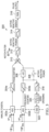
- FIGURE 1 Shown in FIGURE 1 is an example conventional power meter calculation block for AC active or reactive power.
- the block 100 includes a pair of analog-to-digital converters 102a, 102b, for digitizing current I and voltage V, respectively.
- the outputs of the ADCs 102a, 102b are filtered by highpass filters (HPF) 104a, 104b, respectively, to remove offset components.
- HPF highpass filters
- the instantaneous powers include a DC component and a 2 ⁇ component due to the multiplication.
- the instantaneous powers are then lowpass filtered using one or more LPFs 112, 114 to extract the desired quantity.
- the filtering is implemented as a simple IIR (infinite impulse response) first order LPF. As noted above, however, if a PWM 116 is applied at the output of the filtering, then jitter can still result from the 2 ⁇ component.
- Chinese Patent Application CN1439883 discloses an automatic eliminating method for a self DC component in a power metering system.
- a power metering circuit in accordance with embodiments includes a current input path for receiving an analog current input at a first analog to digital converter; a voltage input path for receiving an analog voltage input at a second analog to digital converter; a multiplier configured to multiply an output of the current input path and the voltage input path; a notch filter configured to receive an output of the multiplier, the notch filter having a stop band based on a line frequency; and a control circuit for setting a sampling frequency of the first analog to digital converter and the second analog to digital converter to a multiple of the line frequency.
- control circuit includes a phase locked loop configured to receive one of the analog current input and the analog voltage input.
- control circuit comprises a frequency detector and a programmable oscillator configured to receive an output of the frequency detector.
- the current input path and the voltage input path each including a highpass filter.
- the voltage input path includes a selectable phase shifter.
- the circuit further includes an output pulse width modulator.
- a power metering circuit in accordance with embodiments includes a first input path for receiving one of an analog current input or an analog voltage input at a first analog to digital converter; a second input path for receiving another of the analog voltage input or the analog current input at a second analog to digital converter; a multiplier configured to multiply an output of the first input path and the second input path; and a notch filter configured to receive an output of the multiplier, the notch filter having a stop band based on a line frequency.
- the circuit includes a control circuit for setting a sampling frequency of the first analog to digital converter and the second analog to digital converter to a multiple of the line frequency.
- the control circuit includes a phase locked loop configured to receive one of the analog current input and the analog voltage input.
- the control circuit comprises a frequency detector and a programmable oscillator configured to receive an output of the frequency detector.
- the first input path and the second input path each including a highpass filter.
- the first input path includes a selectable phase shifter.
- the circuit includes an output pulse width modulator.
- a method in accordance with embodiments includes receiving an analog current input at a first analog to digital converter; receiving an analog voltage input at a second analog to digital converter; multiplying an output of the current input path and the voltage input path; notch filtering an output of the multiplier with a stop band based on a line frequency; and setting a sampling frequency of the first analog to digital converter and the second analog to digital converter to a multiple of the line frequency.
- setting the sampling frequency includes using a phase locked loop configured to receive one of the analog current input and the analog voltage input. In some embodiments, setting the sampling frequency comprises using a frequency detector and a programmable oscillator configured to receive an output of the frequency detector. In some embodiments, the current input path and the voltage input path each including a highpass filter. In some embodiments, the voltage input path includes a selectable phase shifter.
- embodiments provide an improved ripple-free calculation block for determining active or reactive power, removing the 2 ⁇ component.
- embodiments use a notch filter to remove the 2 ⁇ component. If the notch filter has a notch at 2 ⁇ , the component is removed and after the filter, the output contains only the desired DC quantity.
- a difficulty can arise, however, because the 2 ⁇ frequency must be known in order to place a notch at the 2 ⁇ frequency.
- the line frequency is not known and can move and change with time, temperature and network inaccuracies.
- embodiments include a control circuit which can track the line frequency and provide the notch at the correct 2 ⁇ frequency.
- a control circuit which can track the line frequency and provide the notch at the correct 2 ⁇ frequency.
- One such embodiment employs a phase-locked loop (PLL) and is shown, for example, in FIGURE 2 .
- PLL phase-locked loop
- the block 200 of FIGURE 2 includes a pair of analog-to-digital converters 202a, 202b, for digitizing current I and voltage V, respectively.
- the outputs of the ADCs 202a, 202b are filtered by highpass filters 204a, 204b, respectively, to remove offset components.
- the current I is multiplied at multiplier 210 with the voltage (switch 208 being closed) to obtain the instantaneous active power or (switch 208 being open), the voltage is applied to phase shifter 206 and then multiplied with the current to obtain the instantaneous reactive power.
- the instantaneous powers include a DC component and a 2 ⁇ component due to the multiplication.
- the 2 ⁇ component is filtered using a notch filter 212 in accordance with embodiments.
- Active or reactive power signal is then filtered at 214 and provided to PWM 216 from which a pulse output is provided.
- a phase locked loop 218 is provided to receive and lock the line frequency.
- the PLL 218 outputs Nf line , which is used by the ADC as the sampling frequency.
- Nf line is used by the ADC as the sampling frequency.
- the data rate of the ADC is a multiple of the line frequency.
- oversampling rate is Nf lin OSR, OSR being the oversampling ratio.
- all calculations are performed at the data rate frequency Nf line .
- the notch filter 212 may be implemented as a first or second order sine filter. In such a case, if the data rate of the ADC is Nf line , an oversampling rate or averaging factor of N/2 can be used to get a notch at precisely the 2fline frequency.
- the N factor depends on the desired bandwidth of the converter. For example, if the application requires convert 32 harmonics of the line frequency, N > 64. Since the PLL has to multiply OSRxN, where OSR is typically between 32 and 512, and N is usually between 8 and 64, the PLL might be a relatively complex analog component.
- FIGURE 3 Such an embodiment is illustrated in FIGURE 3 .
- the block 300 of FIGURE 3 includes a pair of analog-to-digital converters 302a, 302b, for digitizing current I and voltage V, respectively.
- the outputs of the ADCs 302a, 302b are filtered by highpass filters 304a, 304b, respectively, to remove offset components.
- the current I is multiplied at multiplier 310 with the voltage (switch 308 being closed) to obtain the instantaneous active power or (switch 308 being open), the voltage is applied to phase shifter 306 and then multiplied with the current to obtain the instantaneous reactive power.
- the instantaneous powers include a DC component and a 2 ⁇ component due to the multiplication.
- the 2 ⁇ component is filtered using a notch filter 312 in accordance with embodiments.
- Active or reactive power signal is then filtered at 314 and provided to PWM 316 from which a pulse output is provided.
- a control circuit including lowpass filter 318, frequency counter 320, and oscillator 322 is provided.
- the line frequency is measured by LPF 318 (e.g., 1st or second order IIR) to avoid the noise and harmonics to disturb the measurement, followed by a zero-crossing detector and frequency counter 320.
- LPF 318 e.g., 1st or second order IIR
- the line period is then extracted with a number of clock cycles of the frequency detector 320.
- the frequency of the oscillator 322 is then programmed and adjusted as a function of this line frequency detection to be as close as possible to an integer multiple of the line frequency calculated through the zero crossing path.
- the number of clock periods detected should be a power of 2 when the oscillator 322 is tuned so that the data rate can be a power of 2 multiple of the f line .
- the digital processing needed to implement the notch filter is relatively small (a first order sine filter can be implemented with a simple adder) while the frequency evaluation block size remains in most cases substantially smaller than the PLL of the first case.
- the output result after the notch filter is a DC-only component.
- the other advantage the notch filter induces is that it cancels also all the 2 ⁇ components from all the harmonics of the power line. Therefore the output signal is clean of any harmonics, as long as the frequency tracker (PLL, or programmable oscillator with digital processing) tracks correctly the f line frequency.
Landscapes
- Engineering & Computer Science (AREA)
- Physics & Mathematics (AREA)
- General Physics & Mathematics (AREA)
- Power Engineering (AREA)
- Theoretical Computer Science (AREA)
- Mathematical Physics (AREA)
- Stabilization Of Oscillater, Synchronisation, Frequency Synthesizers (AREA)
- Analogue/Digital Conversion (AREA)
Description
- The present disclosure relates to power metering and, in particular, to systems and methods for determining active and reactive power.
- In a simple alternating current (AC) circuit, if the circuit is purely resistive, the current and voltage are in-phase, and true or active power is given by P = VI, in watts. If the loads are purely reactive, i.e., inductive or capacitive, then the voltage and current are ninety (90) degrees out of phase, and reactive power is given in Volt-Amperes-Reactive. In this case, there is no net transfer of energy to the load.
- Practical loads have resistance, inductance, and capacitance, so both true and reactive power will flow to real loads. Even though the current associated with reactive power does no work at the load, it heats the wires, wasting energy.
- In power metering applications, the most common way to measure active and reactive power is to convert current and voltage to digital words or streams with an analog to digital converter (ADC) and then apply a variety of processing to derive active and reactive power. For AC power, the current and voltage both have a fundamental frequency component at the line frequency ω. When doing the instantaneous power calculation, a multiplication is necessary between voltage and current channels. The result of the multiplication contains energy in DC (which is either active or reactive power depending on what quantities have been multiplied) and energy in the 2ω component, where ω is the line frequency. Usually, this result is low pass filtered (LPF) to extract only the DC information but unless a large filter is applied, the remainder of the 2ω is still large enough to create large jitters if a PWM (pulse width modulator) output is connected after the LPF.
- Shown in
FIGURE 1 is an example conventional power meter calculation block for AC active or reactive power. Theblock 100 includes a pair of analog-to-digital converters ADCs multiplier 110 with the voltage (switch 108 being closed) to obtain the instantaneous active power or (switch 108 being open), the voltage is applied tophase shifter 106 and then multiplied with the current to obtain the instantaneous reactive power. - The instantaneous powers include a DC component and a 2ω component due to the multiplication. The instantaneous powers are then lowpass filtered using one or
more LPFs PWM 116 is applied at the output of the filtering, then jitter can still result from the 2ω component. - Chinese Patent Application
CN1439883 discloses an automatic eliminating method for a self DC component in a power metering system. - Accordingly, there is a need for an improved and more stable output for power metering. This and other objects can be achieved by a _power metering system and method as defined in the independent claims. Further enhancements are characterized in the dependent claims.
- According to various embodiments, the 2ω component may be canceled using the systems and methods disclosed herein. A power metering circuit in accordance with embodiments includes a current input path for receiving an analog current input at a first analog to digital converter; a voltage input path for receiving an analog voltage input at a second analog to digital converter; a multiplier configured to multiply an output of the current input path and the voltage input path; a notch filter configured to receive an output of the multiplier, the notch filter having a stop band based on a line frequency; and a control circuit for setting a sampling frequency of the first analog to digital converter and the second analog to digital converter to a multiple of the line frequency.
- In some embodiments, the control circuit includes a phase locked loop configured to receive one of the analog current input and the analog voltage input. In some embodiments, the control circuit comprises a frequency detector and a programmable oscillator configured to receive an output of the frequency detector. In some embodiments, the current input path and the voltage input path each including a highpass filter. In some embodiments, the voltage input path includes a selectable phase shifter. In some embodiments, the circuit further includes an output pulse width modulator.
- A power metering circuit in accordance with embodiments includes a first input path for receiving one of an analog current input or an analog voltage input at a first analog to digital converter; a second input path for receiving another of the analog voltage input or the analog current input at a second analog to digital converter; a multiplier configured to multiply an output of the first input path and the second input path; and a notch filter configured to receive an output of the multiplier, the notch filter having a stop band based on a line frequency.
- In some embodiments, the circuit includes a control circuit for setting a sampling frequency of the first analog to digital converter and the second analog to digital converter to a multiple of the line frequency. In some embodiments, the control circuit includes a phase locked loop configured to receive one of the analog current input and the analog voltage input. In some embodiments, the control circuit comprises a frequency detector and a programmable oscillator configured to receive an output of the frequency detector. In some embodiments, the first input path and the second input path each including a highpass filter. In some embodiments, the first input path includes a selectable phase shifter. In some embodiments, the circuit includes an output pulse width modulator.
- A method in accordance with embodiments includes receiving an analog current input at a first analog to digital converter; receiving an analog voltage input at a second analog to digital converter; multiplying an output of the current input path and the voltage input path; notch filtering an output of the multiplier with a stop band based on a line frequency; and setting a sampling frequency of the first analog to digital converter and the second analog to digital converter to a multiple of the line frequency.
- In some embodiments, setting the sampling frequency includes using a phase locked loop configured to receive one of the analog current input and the analog voltage input. In some embodiments, setting the sampling frequency comprises using a frequency detector and a programmable oscillator configured to receive an output of the frequency detector. In some embodiments, the current input path and the voltage input path each including a highpass filter. In some embodiments, the voltage input path includes a selectable phase shifter.
- The drawings accompanying and forming part of this specification are included to depict certain aspects of the disclosure. It should be noted that the features illustrated in the drawings are not necessarily drawn to scale. A more complete understanding of the disclosure and the advantages thereof may be acquired by referring to the following description, taken in conjunction with the accompanying drawings in which like reference numbers indicate like features and wherein:
-
FIG. 1 is a diagram illustrating an exemplary system according to the prior art. -
FIG. 2 is a diagram illustrating an exemplary system in accordance with embodiments. -
FIG. 3 is a diagram illustrating an exemplary system in accordance with embodiments. - The disclosure and various features and advantageous details thereof arc explained more fully with reference to the exemplary, and therefore non-limiting, embodiments illustrated in the accompanying drawings and detailed in the following description. It should be understood, however, that the detailed description and the specific examples, while indicating the preferred embodiments, are given by way of illustration only and not by way of limitation. Descriptions of known programming techniques, computer software, hardware, operating platforms and protocols may be omitted so as not to unnecessarily obscure the disclosure in detail.
- As will be discussed in greater detail below, embodiments provide an improved ripple-free calculation block for determining active or reactive power, removing the 2ω component. In particular, embodiments use a notch filter to remove the 2ω component. If the notch filter has a notch at 2ω, the component is removed and after the filter, the output contains only the desired DC quantity.
- A difficulty can arise, however, because the 2ω frequency must be known in order to place a notch at the 2ω frequency. Typically, however, the line frequency is not known and can move and change with time, temperature and network inaccuracies.
- Accordingly, embodiments are provided that include a control circuit which can track the line frequency and provide the notch at the correct 2ω frequency. One such embodiment employs a phase-locked loop (PLL) and is shown, for example, in
FIGURE 2 . - The
block 200 ofFIGURE 2 includes a pair of analog-to-digital converters ADCs highpass filters multiplier 210 with the voltage (switch 208 being closed) to obtain the instantaneous active power or (switch 208 being open), the voltage is applied tophase shifter 206 and then multiplied with the current to obtain the instantaneous reactive power. - The instantaneous powers include a DC component and a 2ω component due to the multiplication. The 2ω component is filtered using a
notch filter 212 in accordance with embodiments. Active or reactive power signal is then filtered at 214 and provided to PWM 216 from which a pulse output is provided. - In addition, a phase locked
loop 218 is provided to receive and lock the line frequency. As shown, thePLL 218 outputs Nfline, which is used by the ADC as the sampling frequency. Thus, the data rate of the ADC is a multiple of the line frequency. If the converter is an oversampling converter, then oversampling rate is NflinOSR, OSR being the oversampling ratio. In this case, all calculations are performed at the data rate frequency Nfline. Thenotch filter 212 may be implemented as a first or second order sine filter. In such a case, if the data rate of the ADC is Nfline, an oversampling rate or averaging factor of N/2 can be used to get a notch at precisely the 2fline frequency. - The N factor depends on the desired bandwidth of the converter. For example, if the application requires convert 32 harmonics of the line frequency, N > 64. Since the PLL has to multiply OSRxN, where OSR is typically between 32 and 512, and N is usually between 8 and 64, the PLL might be a relatively complex analog component.
- Consequently, other embodiments may use a programmable master clock oscillator and digital processing blocks as the control circuit. Such an embodiment is illustrated in
FIGURE 3 . Theblock 300 ofFIGURE 3 includes a pair of analog-to-digital converters ADCs highpass filters multiplier 310 with the voltage (switch 308 being closed) to obtain the instantaneous active power or (switch 308 being open), the voltage is applied tophase shifter 306 and then multiplied with the current to obtain the instantaneous reactive power. - The instantaneous powers include a DC component and a 2ω component due to the multiplication. The 2ω component is filtered using a notch filter 312 in accordance with embodiments. Active or reactive power signal is then filtered at 314 and provided to
PWM 316 from which a pulse output is provided. - In addition, a control circuit including
lowpass filter 318,frequency counter 320, andoscillator 322 is provided. In this embodiment, the line frequency is measured by LPF 318 (e.g., 1st or second order IIR) to avoid the noise and harmonics to disturb the measurement, followed by a zero-crossing detector andfrequency counter 320. The line period is then extracted with a number of clock cycles of thefrequency detector 320. The frequency of theoscillator 322 is then programmed and adjusted as a function of this line frequency detection to be as close as possible to an integer multiple of the line frequency calculated through the zero crossing path. - In one embodiment, employing a relatively simple notch filter (sinc with an N/2 averaging rate being a power of 2), the number of clock periods detected should be a power of 2 when the
oscillator 322 is tuned so that the data rate can be a power of 2 multiple of the fline. In such a case the digital processing needed to implement the notch filter is relatively small (a first order sine filter can be implemented with a simple adder) while the frequency evaluation block size remains in most cases substantially smaller than the PLL of the first case. - With both cases of the PLL and frequency evaluation and tuning of the oscillator, the output result after the notch filter is a DC-only component. The other advantage the notch filter induces is that it cancels also all the 2ω components from all the harmonics of the power line. Therefore the output signal is clean of any harmonics, as long as the frequency tracker (PLL, or programmable oscillator with digital processing) tracks correctly the fline frequency.
Claims (15)
- A power metering circuit, comprising:a current input path configured for receiving an analog current input at a first analog to digital converter (202a; 302a);a voltage input path configured for receiving an analog voltage input at a second analog to digital converter (202b; 302b); anda multiplier (210; 310) configured to multiply an output of the current input path and the voltage input path;characterized bya control circuit (218; 318, 320, 322) configured to track a line frequency; anda notch filter (212; 312) configured to receive an output of the multiplier (210; 310), the notch filter (212; 312) having a stop band based on the tracked line frequency (fline); whereinthe control circuit (218; 318, 320, 322) is further configured for setting a sampling frequency of the first analog to digital converter (202a; 302a) and the second analog to digital converter (202b; 302b) to a multiple of the tracked line frequency (fline).
- A power metering circuit in accordance with claim 1, wherein the control circuit includes a phase locked loop (218) configured to receive one of the analog current input and the analog voltage input.
- A power metering circuit in accordance with claim 1 or claim 2, wherein the control circuit comprises a frequency detector (320) and a programmable oscillator (322) configured to receive an output of the frequency detector (320).
- A power metering circuit in accordance with claim 3, wherein the frequency detector (320) is formed by a zero crossing detector and frequency counter (320).
- A power metering circuit in accordance with claim 3 or 4, the control circuit
further comprising a first low pass filter (318) configured to measure the line frequency, coupled with an output of the second analog to digital converter (302b) and providing an input for the frequency detector (320). - A power metering circuit in accordance with one of the preceding claims, the current input path and the voltage input path each including a highpass filter (204a; 304a, 304a; 304b).
- A power metering circuit in accordance with one of the preceding claims, wherein the voltage input path includes a selectable phase shifter (206; 306).
- A power metering circuit in accordance with one of the preceding claims, further comprising a low pass filter (214; 314) coupled with an output of the notch filter (212; 312).
- A power metering circuit in accordance with claim 8, further comprising an output pulse width modulator (216; 316) coupled with an output of the low pass filter (214; 314).
- A method, comprising:receiving an analog current input at a first analog to digital converter (202a; 302a);receiving an analog voltage input at a second analog to digital converter (202b; 302b);multiplying an output of the current input path and the voltage input path by a multiplier (210; 310);characterized bytracking a line frequency with a control circuit(218; 318; 320; 322);notch filtering an output of the multiplier (210; 310) with a stop band based on the tracked line frequency (fline); andsetting a sampling frequency of the first analog to digital converter (202a; 302a) and the second analog to digital converter (202b, 302b) to a multiple of the tracked line frequency (fline).
- A method in accordance with claim 10, wherein setting the sampling frequency includes using a phase locked loop (218) configured to receive one of the analog current input and the analog voltage input.
- A method in accordance with claim 10, -9,- wherein setting the sampling frequency comprises using a frequency detector (320) and a programmable oscillator (322) configured to receive an output of the frequency detector.
- A method in accordance with claim 12, wherein the frequency detector (320) is formed by a zero crossing detector and frequency counter, and preferably further comprising low pass filtering an output of the second analog to digital converter (302b) to measure the line frequency.
- A method in accordance with one of claims 10 to 13 the current input path and the voltage input path each including a highpass filter (204; 304).
- A method in accordance with one of claims 10 to 14, wherein the voltage input path includes a selectable phase shifter (206; 306).
Applications Claiming Priority (2)
| Application Number | Priority Date | Filing Date | Title |
|---|---|---|---|
| US14/669,232 US10197605B2 (en) | 2015-03-26 | 2015-03-26 | System and method for ripple-free AC power determination |
| PCT/US2016/023561 WO2016154192A1 (en) | 2015-03-26 | 2016-03-22 | System and method for ripple-free ac power determination |
Publications (2)
| Publication Number | Publication Date |
|---|---|
| EP3274729A1 EP3274729A1 (en) | 2018-01-31 |
| EP3274729B1 true EP3274729B1 (en) | 2023-07-05 |
Family
ID=55699816
Family Applications (1)
| Application Number | Title | Priority Date | Filing Date |
|---|---|---|---|
| EP16715404.6A Active EP3274729B1 (en) | 2015-03-26 | 2016-03-22 | System and method for ripple-free ac power determination |
Country Status (6)
| Country | Link |
|---|---|
| US (1) | US10197605B2 (en) |
| EP (1) | EP3274729B1 (en) |
| KR (1) | KR20170131397A (en) |
| CN (1) | CN107430159B (en) |
| TW (1) | TW201643443A (en) |
| WO (1) | WO2016154192A1 (en) |
Families Citing this family (5)
| Publication number | Priority date | Publication date | Assignee | Title |
|---|---|---|---|---|
| US9274129B2 (en) | 2006-05-31 | 2016-03-01 | Lpath, Inc. | Methods and reagents for detecting bioactive lipids |
| US10197605B2 (en) * | 2015-03-26 | 2019-02-05 | Microchip Technology Incorporated | System and method for ripple-free AC power determination |
| US11175322B2 (en) * | 2019-12-19 | 2021-11-16 | Landis+Gyr Innovations, Inc. | Gating energy consumption accumulation by detecting a fundamental component of a current |
| US12388429B2 (en) * | 2021-10-14 | 2025-08-12 | Qorvo Us, Inc. | Group delay determination in a communication circuit |
| US12587180B2 (en) | 2021-11-04 | 2026-03-24 | Qorvo Us, Inc. | Group delay determination in a communication circuit |
Citations (1)
| Publication number | Priority date | Publication date | Assignee | Title |
|---|---|---|---|---|
| US8165835B1 (en) * | 2007-10-26 | 2012-04-24 | Cirrus Logic, Inc. | Complex wavelet filter based power measurement and calibration system |
Family Cites Families (37)
| Publication number | Priority date | Publication date | Assignee | Title |
|---|---|---|---|---|
| US3886449A (en) * | 1974-03-06 | 1975-05-27 | Gen Electric | Power measurement circuit |
| US4490688A (en) * | 1981-04-06 | 1984-12-25 | Motorola, Inc. | Digital and analog phase detector for a frequency synthesizer |
| US4399395A (en) * | 1981-09-08 | 1983-08-16 | General Electric Company | Line-to-line voltage reconstruction for synchronizing thyristor power converter |
| GB8426822D0 (en) * | 1984-10-23 | 1984-11-28 | Day S | Static electricity meter |
| US5377092A (en) * | 1992-11-16 | 1994-12-27 | International Power Machines | Method and apparatus for harmonic distortion correction |
| US5349352A (en) * | 1992-12-21 | 1994-09-20 | Harris Corporation | Analog-to-digital converter having high AC line noise rejection and insensitive to AC line frequency variations |
| US5459432A (en) * | 1993-07-22 | 1995-10-17 | Rockwell International Corporation | Use of a chopper and a sigma-delta modulator for downconverting and digitizing an analog signal including information modulated by a carrier |
| US5673196A (en) * | 1995-11-30 | 1997-09-30 | General Electric Company | Vector electricity meters and associated vector electricity metering methods |
| US6417792B1 (en) * | 2000-01-18 | 2002-07-09 | Cirrus Logic, Inc. | Single phase bi-directional electrical measurement systems and methods using ADCs |
| US6329905B1 (en) * | 2000-03-23 | 2001-12-11 | Thalia Products, Inc. | Power line communication system and method |
| CN1195231C (en) * | 2002-02-20 | 2005-03-30 | 北京中星微电子有限公司 | Automatic eliminating method for self d.c. component in power metering system |
| CN1195232C (en) * | 2002-04-27 | 2005-03-30 | 北京中星微电子有限公司 | Simple multiplying circuit for power measurement |
| US6918300B2 (en) * | 2002-06-24 | 2005-07-19 | Koninklijke Philips Electronics N.V. | System and method for determining the resonant frequency and/or amplitude of an oscillating appliance such as a power toothbrush |
| US6943714B2 (en) * | 2002-08-19 | 2005-09-13 | Tdk Semiconductor Corporation | Method and apparatus of obtaining power computation parameters |
| TW587358B (en) * | 2002-11-08 | 2004-05-11 | Uis Abler Electronics Co Ltd | Hybrid virtual work compensating system |
| US6938235B2 (en) * | 2002-11-14 | 2005-08-30 | Cirrus Logic, Inc. | Integrated circuit with authomatic pin-strapping configuration |
| US7015597B2 (en) * | 2003-09-11 | 2006-03-21 | Square D Company | Power regulator for power inverter |
| DE10361664B4 (en) * | 2003-12-30 | 2009-08-13 | Austriamicrosystems Ag | Energy counter arrangement |
| US6977827B2 (en) * | 2004-03-22 | 2005-12-20 | American Superconductor Corporation | Power system having a phase locked loop with a notch filter |
| US7395290B2 (en) * | 2004-06-04 | 2008-07-01 | Agilent Technologies, Inc. | Digital filter and method thereof using frequency translations |
| US20060062291A1 (en) * | 2004-09-20 | 2006-03-23 | Honeywell International Inc. | Digital pulse width modulated controller |
| BRPI0610827A2 (en) * | 2005-05-17 | 2010-07-27 | Siemens Energy & Automat | multilevel active filter |
| US20070067119A1 (en) * | 2005-09-16 | 2007-03-22 | Power Measurement Ltd. | Rack-mounted power meter having removable metering options module |
| US7475801B2 (en) * | 2005-12-29 | 2009-01-13 | Dukane Corporation | Systems for providing controlled power to ultrasonic welding probes |
| US7778053B2 (en) * | 2006-02-13 | 2010-08-17 | American Superconductor Corp. | Power system having a voltage regulator with a notch filter |
| CN100439926C (en) * | 2006-03-31 | 2008-12-03 | 北京万工科技有限公司 | Integrator for Rogowski Coil and Its Realization Method |
| US7425874B2 (en) * | 2006-06-30 | 2008-09-16 | Texas Instruments Incorporated | All-digital phase-locked loop for a digital pulse-width modulator |
| US7626837B2 (en) * | 2006-08-14 | 2009-12-01 | Agere Systems Inc. | Digitally controlled current-mode switched power supply |
| WO2008084851A1 (en) * | 2007-01-12 | 2008-07-17 | Panasonic Corporation | Transmission device and transmission power control method |
| TWI347058B (en) * | 2007-03-05 | 2011-08-11 | Ablerex Electronics Co Ltd | Active power filter apparatus |
| US8010304B2 (en) * | 2008-10-03 | 2011-08-30 | Analog Devices, Inc. | Apparatus and method for measuring active and reactive powers |
| WO2012079151A1 (en) * | 2010-12-15 | 2012-06-21 | Triacta Power Technologies, Inc. | Wireless voltage reference broadcast in a distributed energy metering system |
| US8868364B2 (en) * | 2011-04-29 | 2014-10-21 | Analog Devices, Inc. | Apparatus and method for real time harmonic spectral analyzer |
| US20130077360A1 (en) * | 2011-09-26 | 2013-03-28 | Qualcomm Incorporated | Systems, methods, and apparatus for rectifier filtering for input waveform shaping |
| CN103532412A (en) * | 2012-07-05 | 2014-01-22 | 台达电子工业股份有限公司 | Feedback control circuit and power converter system of a power converter |
| US9201104B2 (en) * | 2012-10-08 | 2015-12-01 | Tyco Electronics Corporation | Intelligent power sensing device |
| US10197605B2 (en) * | 2015-03-26 | 2019-02-05 | Microchip Technology Incorporated | System and method for ripple-free AC power determination |
-
2015
- 2015-03-26 US US14/669,232 patent/US10197605B2/en active Active
-
2016
- 2016-03-22 CN CN201680016330.7A patent/CN107430159B/en active Active
- 2016-03-22 EP EP16715404.6A patent/EP3274729B1/en active Active
- 2016-03-22 KR KR1020177025503A patent/KR20170131397A/en not_active Withdrawn
- 2016-03-22 WO PCT/US2016/023561 patent/WO2016154192A1/en not_active Ceased
- 2016-03-25 TW TW105109517A patent/TW201643443A/en unknown
Patent Citations (1)
| Publication number | Priority date | Publication date | Assignee | Title |
|---|---|---|---|---|
| US8165835B1 (en) * | 2007-10-26 | 2012-04-24 | Cirrus Logic, Inc. | Complex wavelet filter based power measurement and calibration system |
Also Published As
| Publication number | Publication date |
|---|---|
| EP3274729A1 (en) | 2018-01-31 |
| CN107430159B (en) | 2023-11-10 |
| US20160282391A1 (en) | 2016-09-29 |
| US10197605B2 (en) | 2019-02-05 |
| CN107430159A (en) | 2017-12-01 |
| WO2016154192A1 (en) | 2016-09-29 |
| KR20170131397A (en) | 2017-11-29 |
| TW201643443A (en) | 2016-12-16 |
Similar Documents
| Publication | Publication Date | Title |
|---|---|---|
| US10197605B2 (en) | System and method for ripple-free AC power determination | |
| CA2425496C (en) | Fast phase synchronization and retrieval of sequence components in three-phase networks | |
| CN101617234B (en) | Advanced real-time grid monitoring system | |
| US7956694B1 (en) | Phase controlled dimmer using a narrow band quadrature demodulator | |
| KR102427375B1 (en) | Phase lock loop circuit having a wide bandwidth | |
| CA2898640C (en) | Methods and devices for determining root mean square of a delta-sigma modulated signal | |
| US8868364B2 (en) | Apparatus and method for real time harmonic spectral analyzer | |
| Golestan et al. | Open-loop synchronization systems for grid-tied power converters: Literature overview, design considerations, advantages, and disadvantages | |
| CN100462725C (en) | Meters for Metering Electric Power | |
| CN102832931A (en) | Phase demodulation method, phase demodulation device and phase-locked loop based on incomplete period grid voltage signal | |
| JP2002541692A (en) | Digital phase sensitive rectification of signals from AC driven transducers | |
| CN1963541A (en) | Electric energy computation circuit removing DC and circuit removing DC | |
| Reza et al. | A method without stability issue for robust estimation of three-phase grid frequency | |
| Tyagi et al. | Finer granularity DFT bins with moving window for capacitance sensing | |
| Marques et al. | Enhanced demodulation-based technique for estimating the parameters of fundamental component in power systems | |
| RS59943B1 (en) | Frequency multiplying device | |
| US9160308B2 (en) | Synchronous charge sharing filter | |
| JP2587970B2 (en) | Impedance measuring device | |
| KR100964114B1 (en) | Phaser measuring device | |
| Zhang et al. | An innovative timestamp-based convolution integral method in synchrophasor estimation within digital relays | |
| Santos et al. | A Fourier-based PLL for single-phase grid connected systems | |
| Ashraf et al. | A novel PLL technique using digital lock-in amplifier under distorted grid conditions | |
| US4973914A (en) | Digitized synchronous demodulator | |
| Serov et al. | The Method of Reducing the Active Power Measurement Error With Non-Simultaneous Sampling of Voltage and Current | |
| RU2222068C1 (en) | Synchronization relay |
Legal Events
| Date | Code | Title | Description |
|---|---|---|---|
| STAA | Information on the status of an ep patent application or granted ep patent |
Free format text: STATUS: THE INTERNATIONAL PUBLICATION HAS BEEN MADE |
|
| PUAI | Public reference made under article 153(3) epc to a published international application that has entered the european phase |
Free format text: ORIGINAL CODE: 0009012 |
|
| STAA | Information on the status of an ep patent application or granted ep patent |
Free format text: STATUS: REQUEST FOR EXAMINATION WAS MADE |
|
| 17P | Request for examination filed |
Effective date: 20171020 |
|
| AK | Designated contracting states |
Kind code of ref document: A1 Designated state(s): AL AT BE BG CH CY CZ DE DK EE ES FI FR GB GR HR HU IE IS IT LI LT LU LV MC MK MT NL NO PL PT RO RS SE SI SK SM TR |
|
| AX | Request for extension of the european patent |
Extension state: BA ME |
|
| DAV | Request for validation of the european patent (deleted) | ||
| DAX | Request for extension of the european patent (deleted) | ||
| STAA | Information on the status of an ep patent application or granted ep patent |
Free format text: STATUS: EXAMINATION IS IN PROGRESS |
|
| 17Q | First examination report despatched |
Effective date: 20201217 |
|
| GRAP | Despatch of communication of intention to grant a patent |
Free format text: ORIGINAL CODE: EPIDOSNIGR1 |
|
| STAA | Information on the status of an ep patent application or granted ep patent |
Free format text: STATUS: GRANT OF PATENT IS INTENDED |
|
| INTG | Intention to grant announced |
Effective date: 20230124 |
|
| GRAS | Grant fee paid |
Free format text: ORIGINAL CODE: EPIDOSNIGR3 |
|
| GRAA | (expected) grant |
Free format text: ORIGINAL CODE: 0009210 |
|
| STAA | Information on the status of an ep patent application or granted ep patent |
Free format text: STATUS: THE PATENT HAS BEEN GRANTED |
|
| AK | Designated contracting states |
Kind code of ref document: B1 Designated state(s): AL AT BE BG CH CY CZ DE DK EE ES FI FR GB GR HR HU IE IS IT LI LT LU LV MC MK MT NL NO PL PT RO RS SE SI SK SM TR |
|
| REG | Reference to a national code |
Ref country code: CH Ref legal event code: EP |
|
| REG | Reference to a national code |
Ref country code: AT Ref legal event code: REF Ref document number: 1585321 Country of ref document: AT Kind code of ref document: T Effective date: 20230715 |
|
| REG | Reference to a national code |
Ref country code: DE Ref legal event code: R096 Ref document number: 602016080788 Country of ref document: DE |
|
| REG | Reference to a national code |
Ref country code: IE Ref legal event code: FG4D |
|
| REG | Reference to a national code |
Ref country code: LT Ref legal event code: MG9D |
|
| REG | Reference to a national code |
Ref country code: NL Ref legal event code: MP Effective date: 20230705 |
|
| REG | Reference to a national code |
Ref country code: AT Ref legal event code: MK05 Ref document number: 1585321 Country of ref document: AT Kind code of ref document: T Effective date: 20230705 |
|
| PG25 | Lapsed in a contracting state [announced via postgrant information from national office to epo] |
Ref country code: NL Free format text: LAPSE BECAUSE OF FAILURE TO SUBMIT A TRANSLATION OF THE DESCRIPTION OR TO PAY THE FEE WITHIN THE PRESCRIBED TIME-LIMIT Effective date: 20230705 |
|
| PG25 | Lapsed in a contracting state [announced via postgrant information from national office to epo] |
Ref country code: GR Free format text: LAPSE BECAUSE OF FAILURE TO SUBMIT A TRANSLATION OF THE DESCRIPTION OR TO PAY THE FEE WITHIN THE PRESCRIBED TIME-LIMIT Effective date: 20231006 |
|
| PG25 | Lapsed in a contracting state [announced via postgrant information from national office to epo] |
Ref country code: ES Free format text: LAPSE BECAUSE OF FAILURE TO SUBMIT A TRANSLATION OF THE DESCRIPTION OR TO PAY THE FEE WITHIN THE PRESCRIBED TIME-LIMIT Effective date: 20230705 |
|
| PG25 | Lapsed in a contracting state [announced via postgrant information from national office to epo] |
Ref country code: IS Free format text: LAPSE BECAUSE OF FAILURE TO SUBMIT A TRANSLATION OF THE DESCRIPTION OR TO PAY THE FEE WITHIN THE PRESCRIBED TIME-LIMIT Effective date: 20231105 |
|
| PG25 | Lapsed in a contracting state [announced via postgrant information from national office to epo] |
Ref country code: SE Free format text: LAPSE BECAUSE OF FAILURE TO SUBMIT A TRANSLATION OF THE DESCRIPTION OR TO PAY THE FEE WITHIN THE PRESCRIBED TIME-LIMIT Effective date: 20230705 Ref country code: RS Free format text: LAPSE BECAUSE OF FAILURE TO SUBMIT A TRANSLATION OF THE DESCRIPTION OR TO PAY THE FEE WITHIN THE PRESCRIBED TIME-LIMIT Effective date: 20230705 Ref country code: PT Free format text: LAPSE BECAUSE OF FAILURE TO SUBMIT A TRANSLATION OF THE DESCRIPTION OR TO PAY THE FEE WITHIN THE PRESCRIBED TIME-LIMIT Effective date: 20231106 Ref country code: NO Free format text: LAPSE BECAUSE OF FAILURE TO SUBMIT A TRANSLATION OF THE DESCRIPTION OR TO PAY THE FEE WITHIN THE PRESCRIBED TIME-LIMIT Effective date: 20231005 Ref country code: LV Free format text: LAPSE BECAUSE OF FAILURE TO SUBMIT A TRANSLATION OF THE DESCRIPTION OR TO PAY THE FEE WITHIN THE PRESCRIBED TIME-LIMIT Effective date: 20230705 Ref country code: LT Free format text: LAPSE BECAUSE OF FAILURE TO SUBMIT A TRANSLATION OF THE DESCRIPTION OR TO PAY THE FEE WITHIN THE PRESCRIBED TIME-LIMIT Effective date: 20230705 Ref country code: IS Free format text: LAPSE BECAUSE OF FAILURE TO SUBMIT A TRANSLATION OF THE DESCRIPTION OR TO PAY THE FEE WITHIN THE PRESCRIBED TIME-LIMIT Effective date: 20231105 Ref country code: HR Free format text: LAPSE BECAUSE OF FAILURE TO SUBMIT A TRANSLATION OF THE DESCRIPTION OR TO PAY THE FEE WITHIN THE PRESCRIBED TIME-LIMIT Effective date: 20230705 Ref country code: GR Free format text: LAPSE BECAUSE OF FAILURE TO SUBMIT A TRANSLATION OF THE DESCRIPTION OR TO PAY THE FEE WITHIN THE PRESCRIBED TIME-LIMIT Effective date: 20231006 Ref country code: FI Free format text: LAPSE BECAUSE OF FAILURE TO SUBMIT A TRANSLATION OF THE DESCRIPTION OR TO PAY THE FEE WITHIN THE PRESCRIBED TIME-LIMIT Effective date: 20230705 Ref country code: ES Free format text: LAPSE BECAUSE OF FAILURE TO SUBMIT A TRANSLATION OF THE DESCRIPTION OR TO PAY THE FEE WITHIN THE PRESCRIBED TIME-LIMIT Effective date: 20230705 Ref country code: AT Free format text: LAPSE BECAUSE OF FAILURE TO SUBMIT A TRANSLATION OF THE DESCRIPTION OR TO PAY THE FEE WITHIN THE PRESCRIBED TIME-LIMIT Effective date: 20230705 |
|
| PG25 | Lapsed in a contracting state [announced via postgrant information from national office to epo] |
Ref country code: PL Free format text: LAPSE BECAUSE OF FAILURE TO SUBMIT A TRANSLATION OF THE DESCRIPTION OR TO PAY THE FEE WITHIN THE PRESCRIBED TIME-LIMIT Effective date: 20230705 |
|
| REG | Reference to a national code |
Ref country code: DE Ref legal event code: R097 Ref document number: 602016080788 Country of ref document: DE |
|
| PG25 | Lapsed in a contracting state [announced via postgrant information from national office to epo] |
Ref country code: SM Free format text: LAPSE BECAUSE OF FAILURE TO SUBMIT A TRANSLATION OF THE DESCRIPTION OR TO PAY THE FEE WITHIN THE PRESCRIBED TIME-LIMIT Effective date: 20230705 Ref country code: RO Free format text: LAPSE BECAUSE OF FAILURE TO SUBMIT A TRANSLATION OF THE DESCRIPTION OR TO PAY THE FEE WITHIN THE PRESCRIBED TIME-LIMIT Effective date: 20230705 Ref country code: EE Free format text: LAPSE BECAUSE OF FAILURE TO SUBMIT A TRANSLATION OF THE DESCRIPTION OR TO PAY THE FEE WITHIN THE PRESCRIBED TIME-LIMIT Effective date: 20230705 Ref country code: DK Free format text: LAPSE BECAUSE OF FAILURE TO SUBMIT A TRANSLATION OF THE DESCRIPTION OR TO PAY THE FEE WITHIN THE PRESCRIBED TIME-LIMIT Effective date: 20230705 Ref country code: CZ Free format text: LAPSE BECAUSE OF FAILURE TO SUBMIT A TRANSLATION OF THE DESCRIPTION OR TO PAY THE FEE WITHIN THE PRESCRIBED TIME-LIMIT Effective date: 20230705 Ref country code: SK Free format text: LAPSE BECAUSE OF FAILURE TO SUBMIT A TRANSLATION OF THE DESCRIPTION OR TO PAY THE FEE WITHIN THE PRESCRIBED TIME-LIMIT Effective date: 20230705 |
|
| PLBE | No opposition filed within time limit |
Free format text: ORIGINAL CODE: 0009261 |
|
| STAA | Information on the status of an ep patent application or granted ep patent |
Free format text: STATUS: NO OPPOSITION FILED WITHIN TIME LIMIT |
|
| PG25 | Lapsed in a contracting state [announced via postgrant information from national office to epo] |
Ref country code: IT Free format text: LAPSE BECAUSE OF FAILURE TO SUBMIT A TRANSLATION OF THE DESCRIPTION OR TO PAY THE FEE WITHIN THE PRESCRIBED TIME-LIMIT Effective date: 20230705 |
|
| 26N | No opposition filed |
Effective date: 20240408 |
|
| PG25 | Lapsed in a contracting state [announced via postgrant information from national office to epo] |
Ref country code: SI Free format text: LAPSE BECAUSE OF FAILURE TO SUBMIT A TRANSLATION OF THE DESCRIPTION OR TO PAY THE FEE WITHIN THE PRESCRIBED TIME-LIMIT Effective date: 20230705 |
|
| REG | Reference to a national code |
Ref country code: CH Ref legal event code: PL |
|
| PG25 | Lapsed in a contracting state [announced via postgrant information from national office to epo] |
Ref country code: BG Free format text: LAPSE BECAUSE OF FAILURE TO SUBMIT A TRANSLATION OF THE DESCRIPTION OR TO PAY THE FEE WITHIN THE PRESCRIBED TIME-LIMIT Effective date: 20230705 |
|
| PG25 | Lapsed in a contracting state [announced via postgrant information from national office to epo] |
Ref country code: LU Free format text: LAPSE BECAUSE OF NON-PAYMENT OF DUE FEES Effective date: 20240322 |
|
| PG25 | Lapsed in a contracting state [announced via postgrant information from national office to epo] |
Ref country code: MC Free format text: LAPSE BECAUSE OF FAILURE TO SUBMIT A TRANSLATION OF THE DESCRIPTION OR TO PAY THE FEE WITHIN THE PRESCRIBED TIME-LIMIT Effective date: 20230705 |
|
| GBPC | Gb: european patent ceased through non-payment of renewal fee |
Effective date: 20240322 |
|
| PG25 | Lapsed in a contracting state [announced via postgrant information from national office to epo] |
Ref country code: MC Free format text: LAPSE BECAUSE OF FAILURE TO SUBMIT A TRANSLATION OF THE DESCRIPTION OR TO PAY THE FEE WITHIN THE PRESCRIBED TIME-LIMIT Effective date: 20230705 Ref country code: LU Free format text: LAPSE BECAUSE OF NON-PAYMENT OF DUE FEES Effective date: 20240322 Ref country code: BG Free format text: LAPSE BECAUSE OF FAILURE TO SUBMIT A TRANSLATION OF THE DESCRIPTION OR TO PAY THE FEE WITHIN THE PRESCRIBED TIME-LIMIT Effective date: 20230705 |
|
| REG | Reference to a national code |
Ref country code: BE Ref legal event code: MM Effective date: 20240331 |
|
| PG25 | Lapsed in a contracting state [announced via postgrant information from national office to epo] |
Ref country code: BE Free format text: LAPSE BECAUSE OF NON-PAYMENT OF DUE FEES Effective date: 20240331 |
|
| PG25 | Lapsed in a contracting state [announced via postgrant information from national office to epo] |
Ref country code: GB Free format text: LAPSE BECAUSE OF NON-PAYMENT OF DUE FEES Effective date: 20240322 |
|
| PG25 | Lapsed in a contracting state [announced via postgrant information from national office to epo] |
Ref country code: IE Free format text: LAPSE BECAUSE OF NON-PAYMENT OF DUE FEES Effective date: 20240322 |
|
| PG25 | Lapsed in a contracting state [announced via postgrant information from national office to epo] |
Ref country code: IE Free format text: LAPSE BECAUSE OF NON-PAYMENT OF DUE FEES Effective date: 20240322 Ref country code: GB Free format text: LAPSE BECAUSE OF NON-PAYMENT OF DUE FEES Effective date: 20240322 Ref country code: BE Free format text: LAPSE BECAUSE OF NON-PAYMENT OF DUE FEES Effective date: 20240331 Ref country code: CH Free format text: LAPSE BECAUSE OF NON-PAYMENT OF DUE FEES Effective date: 20240331 |
|
| PG25 | Lapsed in a contracting state [announced via postgrant information from national office to epo] |
Ref country code: CY Free format text: LAPSE BECAUSE OF FAILURE TO SUBMIT A TRANSLATION OF THE DESCRIPTION OR TO PAY THE FEE WITHIN THE PRESCRIBED TIME-LIMIT; INVALID AB INITIO Effective date: 20160322 |
|
| PG25 | Lapsed in a contracting state [announced via postgrant information from national office to epo] |
Ref country code: HU Free format text: LAPSE BECAUSE OF FAILURE TO SUBMIT A TRANSLATION OF THE DESCRIPTION OR TO PAY THE FEE WITHIN THE PRESCRIBED TIME-LIMIT; INVALID AB INITIO Effective date: 20160322 |
|
| PG25 | Lapsed in a contracting state [announced via postgrant information from national office to epo] |
Ref country code: TR Free format text: LAPSE BECAUSE OF FAILURE TO SUBMIT A TRANSLATION OF THE DESCRIPTION OR TO PAY THE FEE WITHIN THE PRESCRIBED TIME-LIMIT Effective date: 20230705 |
|
| PGFP | Annual fee paid to national office [announced via postgrant information from national office to epo] |
Ref country code: DE Payment date: 20260219 Year of fee payment: 11 |
|
| PGFP | Annual fee paid to national office [announced via postgrant information from national office to epo] |
Ref country code: FR Payment date: 20260219 Year of fee payment: 11 |