EP3273537A1 - Signal distributing/combining apparatus in antenna apparatus of mobile communication base station - Google Patents
Signal distributing/combining apparatus in antenna apparatus of mobile communication base station Download PDFInfo
- Publication number
- EP3273537A1 EP3273537A1 EP15885679.9A EP15885679A EP3273537A1 EP 3273537 A1 EP3273537 A1 EP 3273537A1 EP 15885679 A EP15885679 A EP 15885679A EP 3273537 A1 EP3273537 A1 EP 3273537A1
- Authority
- EP
- European Patent Office
- Prior art keywords
- circuit board
- signal distributing
- combining
- support plate
- signal
- Prior art date
- Legal status (The legal status is an assumption and is not a legal conclusion. Google has not performed a legal analysis and makes no representation as to the accuracy of the status listed.)
- Granted
Links
Images











Classifications
-
- H—ELECTRICITY
- H01—ELECTRIC ELEMENTS
- H01Q—ANTENNAS, i.e. RADIO AERIALS
- H01Q1/00—Details of, or arrangements associated with, antennas
- H01Q1/12—Supports; Mounting means
- H01Q1/22—Supports; Mounting means by structural association with other equipment or articles
- H01Q1/24—Supports; Mounting means by structural association with other equipment or articles with receiving set
- H01Q1/241—Supports; Mounting means by structural association with other equipment or articles with receiving set used in mobile communications, e.g. GSM
- H01Q1/246—Supports; Mounting means by structural association with other equipment or articles with receiving set used in mobile communications, e.g. GSM specially adapted for base stations
-
- H—ELECTRICITY
- H01—ELECTRIC ELEMENTS
- H01P—WAVEGUIDES; RESONATORS, LINES, OR OTHER DEVICES OF THE WAVEGUIDE TYPE
- H01P5/00—Coupling devices of the waveguide type
- H01P5/08—Coupling devices of the waveguide type for linking dissimilar lines or devices
- H01P5/085—Coaxial-line/strip-line transitions
-
- H—ELECTRICITY
- H01—ELECTRIC ELEMENTS
- H01P—WAVEGUIDES; RESONATORS, LINES, OR OTHER DEVICES OF THE WAVEGUIDE TYPE
- H01P5/00—Coupling devices of the waveguide type
- H01P5/12—Coupling devices having more than two ports
- H01P5/16—Conjugate devices, i.e. devices having at least one port decoupled from one other port
-
- H—ELECTRICITY
- H01—ELECTRIC ELEMENTS
- H01Q—ANTENNAS, i.e. RADIO AERIALS
- H01Q1/00—Details of, or arrangements associated with, antennas
- H01Q1/36—Structural form of radiating elements, e.g. cone, spiral, umbrella; Particular materials used therewith
- H01Q1/38—Structural form of radiating elements, e.g. cone, spiral, umbrella; Particular materials used therewith formed by a conductive layer on an insulating support
-
- H—ELECTRICITY
- H01—ELECTRIC ELEMENTS
- H01Q—ANTENNAS, i.e. RADIO AERIALS
- H01Q1/00—Details of, or arrangements associated with, antennas
- H01Q1/44—Details of, or arrangements associated with, antennas using equipment having another main function to serve additionally as an antenna, e.g. means for giving an antenna an aesthetic aspect
- H01Q1/46—Electric supply lines or communication lines
-
- H—ELECTRICITY
- H01—ELECTRIC ELEMENTS
- H01Q—ANTENNAS, i.e. RADIO AERIALS
- H01Q15/00—Devices for reflection, refraction, diffraction or polarisation of waves radiated from an antenna, e.g. quasi-optical devices
- H01Q15/14—Reflecting surfaces; Equivalent structures
-
- H—ELECTRICITY
- H01—ELECTRIC ELEMENTS
- H01R—ELECTRICALLY-CONDUCTIVE CONNECTIONS; STRUCTURAL ASSOCIATIONS OF A PLURALITY OF MUTUALLY-INSULATED ELECTRICAL CONNECTING ELEMENTS; COUPLING DEVICES; CURRENT COLLECTORS
- H01R9/00—Structural associations of a plurality of mutually-insulated electrical connecting elements, e.g. terminal strips or terminal blocks; Terminals or binding posts mounted upon a base or in a case; Bases therefor
- H01R9/03—Connectors arranged to contact a plurality of the conductors of a multiconductor cable, e.g. tapping connections
- H01R9/05—Connectors arranged to contact a plurality of the conductors of a multiconductor cable, e.g. tapping connections for coaxial cables
- H01R9/0515—Connection to a rigid planar substrate, e.g. printed circuit board
Definitions
- the present disclosure relates to an antenna device applicable to a base station and a relay station in a mobile communication (PCS, cellular, CDMA, GSM, LTE, etc.) network. More particularly, the present disclosure in some embodiments relates to a signal distributing/combining apparatus for distributing or combining radio frequency (RF) signals in an antenna device.
- PCS mobile communication
- cellular Code Division Multiple Access
- CDMA Code Division Multiple Access
- GSM Global System for Mobile communications
- LTE long-term evolution
- the present disclosure in some embodiments relates to a signal distributing/combining apparatus for distributing or combining radio frequency (RF) signals in an antenna device.
- RF radio frequency
- a base station or a relay station (hereinafter collectively referred to as "base station") of a mobile communication system has been divided into a base station main unit configured to process transmit and receive signals and an antenna device including a plurality of radiating elements for transmitting/receiving radio signals.
- the base station main unit is usually installed at a low position on the ground, and the antenna device is installed at a high position such as a building roof or a tower, and the base station main unit and the antenna device may be connected to each other through a feeding cable or the like.
- the antenna device of the base station includes a plurality of radiating elements for transmitting/receiving high frequency radio signals.
- the radiating elements are installed on one surface (for example, the front surface) of a metal reflecting plate having a relatively large area.
- the antenna device is provided with various circuits or devices for processing signals transmitted and received via the plurality of radiating elements, and, for example, the circuits or devices may be fixedly installed on the back face of the reflecting plate.
- Such devices may include a phase shifter for adjusting the phase of the signals of the multiple radiating elements, and an apparatus for distributing/combining the transmit and receive signals of the internal devices and the radiating elements.
- the respective devices may be connected via a signal transmission line, and a substantial portion of which is formed of coaxial cable.
- the antenna device almost invariably requires a signal distributing/combining apparatus and the structure for making connections through soldering a coaxial cable to that signal distributing/combining apparatus, which in turn requires effective measures to suppress PIMD that can be generated due to unstable connection state occurring at the connections between the signal distributing/combining apparatus and the coaxial cable or due to nonuniform soldering state, etc.
- the present disclosure seeks to provide a signal distributing/combining apparatus in a mobile communication base station antenna apparatus, which is capable of suppressing the PIMD generated at the connection with the coaxial cable, stabilizing the quality of soldering at the connection, and stabilizing the grounding quality of the apparatus.
- a signal distributing/combining apparatus in an antenna device of a mobile communication base station includes a circuit board and a support plate.
- the circuit board is configured to have an upper surface formed with a signal distributing/combining conductor pattern for a high frequency signal distributing/combining operation.
- the support plate is configured to have an upper mounting surface of a size corresponding to the circuit board, to mate with the circuit board so that an underside of the circuit board is in close contact with the upper mounting surface for supporting the circuit board, and to fixedly mate with the antenna device at a reflection plate on a bottom side of the support plate.
- the support plate is provided with a plurality of cable holders for supporting and fixating coaxial cables for signal transmission, which are connected from outside of the signal distributing/combining apparatus, the signal distributing/combining conductor pattern is formed with a plurality of signal input/output portions.
- the plurality of cable holders is formed on the signal distributing/combining conductor pattern at portions corresponding to at least some of a plurality of signal input/output portions, the cable holders having a structure formed elongated longitudinally and corresponding to outer conductors of the coaxial cables in order to mount the coaxial cable by inserting the outer conductors.
- the cable holders may be formed at predetermined positions in the support plate such that inner conductors of the coaxial cables are placed in contact with the upper surface of the circuit board.
- the underside of the circuit board and the upper mounting surface of the support plate for mounting the circuit board may be bonded together with a solder cream which is melted and cured with a reflow soldering method.
- the upper surface of the circuit board may be formed with a coupling conductor pattern for generating a coupling signal in a non-contact coupling scheme with the signal distributing/combining conductor pattern.
- the upper surface of the circuit board may be formed with a ground conductor pattern in a peripheral region adjacent to the signal distributing/combining conductor pattern and the coupling conductor pattern, and the ground conductor pattern may have a plurality of via holes for making an electrical connection with grounding layer on the underside of the circuit board.
- the support plate may have open areas, and include a plurality of cable holders corresponding respectively to the coaxial cables for mounting the coaxial cables connected to the underside of the circuit board after passing through the open areas.
- the support plate may include multiple fastening protrusions which protrude downwardly of the support plate and are respectively formed with screw fastening recesses for screw fastening with a reflection plate of the antenna device.
- the support plate may include a mounting surface configured to mount the circuit board and to have one or more partition members formed in a predetermined length and a predetermined height.
- the circuit board may have one or more slots to be coupled with the partition members in such a manner that the partition members are inserted.
- the partition members may be formed so as to protrude from the upper surface of the circuit board on which the conductor pattern is formed to a preset height.
- the signal distributing/combining apparatus in the mobile communication base station antenna device can suppress the PIMD generated at the connection with the cable, stabilize the quality of the soldering at the connection, and stabilize the grounding quality of the apparatus.
- FIG. 1 is a schematic of a structure of a mobile communication base station antenna device to which a signal distributing/combining apparatus according to at least one embodiment of the present disclosure is applied.
- the base station antenna device is configured as a metal plate having a relatively large area as a whole, and includes a reflection plate 1, an upper phase shifter 6, a lower phase shifter 5, a radome 4, a lower cap 2 and an upper cap 3.
- the reflection plate 1 has one side (e.g., the front side) mounted with a plurality of radiating elements (not shown) for transmitting/receiving radio signals.
- the upper and lower phase shifters 6, 5 are installed high and low on the other side (e.g., the rear side) of the reflection plate 1, and adjust the phases of the signals of the multiple radiation elements.
- the radome 4 is formed in an integrated cylindrical shape to surround interior devices of the antenna including the reflection plate 1 and the upper and lower phase shifters 6, 5.
- the lower cap 2 and the upper cap 3 fixate upper and lower portions of the reflecting plate 1 respectively, and sealingly join with the upper and lower open portions of the cylindrical radome 4.
- a signal distributing/combining apparatus 7 may be provided, for example, in a central portion on the back surface of the reflection plate 1 of the antenna device.
- the signal distributing/combining apparatus 7 receives transmitted signals input from the base station's main unit device (not shown) outside the antenna device and distributes the input signals to the antenna's interior devices including the upper and lower phase shifters 6, 5, and it combines the receive signals received via the radiating elements of the antenna device and outputs the combined signals to the base station main unit side.
- the radome 4 of the antenna device may be provided with other additional distributing/combining circuits, or amplifiers, filters, etc. and it may be appropriately installed with various electronic components (not shown) such as a detection circuit for detecting various operational states of the antenna including signal transmission quality and a main control device (e.g., an MCU etc.) for controlling the overall operation.
- various electronic components such as a detection circuit for detecting various operational states of the antenna including signal transmission quality and a main control device (e.g., an MCU etc.) for controlling the overall operation.
- a main control device e.g., an MCU etc.
- the lower cap 2 is usually installed with a plurality of input/output connectors 202 for inputting/outputting transmit/receive signals to and from the antenna device.
- the input/output connectors 202 may be directly or indirectly connected to the base station main unit side via a plurality of power supply cables 8.
- a plurality of coaxial cables 22 may be used as signal transmission transmission lines between the input/output connectors 202 of the lower cap 2 and the signal distributing/combining apparatus 7.
- the signal distributing/combining apparatus 7 may be connected with the upper and lower phase shifters 6, 5 via coaxial cables 73, 71, respectively.
- FIG. 1 illustrates the upper and lower phase thousands 6, 5 provided in the antenna device, although a different structure of antenna device may be provided with, for example, a single phase shifter.
- the relevant phase shifter may be installed centrally of the back surface of the reflection plate, and the signal distributing/combining apparatus may be installed in the lower part of the back surface of the reflection plate.
- the relevant signal distributing/combining apparatus may also be configured to distribute signals to another device (other devices) including the above-mentioned single phase shifter and the radiating elements. In this manner, the installation position of the signal distributing/combining apparatus and its connection structure with other devices may be appropriately set so as to match the antenna device implemented with various structures.
- the signal distributing/combining apparatus 7 may be mainly provided with a printed circuit board on which a conductor pattern is formed for high frequency signal distributing/combining.
- a method of soldering the inner conductor of the coaxial cable to the input/output end of the conductor pattern it is typical to apply a method of soldering the inner conductor of the coaxial cable to the input/output end of the conductor pattern.
- the signal distributing/combining apparatus 7 according to some embodiments, as will be described later, provides a structure capable of suppressing the occurrence of PIMD, particularly at the connecting portion of the coaxial cable.
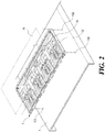
- FIG. 2 is a perspective view of the signal distributing/combining apparatus 7 according to at least one embodiment of the present disclosure, further illustrating the reflector 1.
- FIG. 3 is an exploded perspective view of a circuit board 74 and a support plate 72 of the signal distributing/combining apparatus 7 of FIG. 2 .
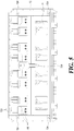
- FIGS. 4 and 5 are respectively a plan view and a rear view of the signal distributing/combining apparatus 7 of FIG. 2 .
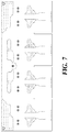
- FIGS. 6 and 7 are respectively a plan view and a rear view of the circuit board 74 of the signal distributing/combining apparatus 7 of FIG. 2 .
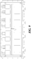
- FIGS. 8 to 11 are respectively a plan view, a rear view, a first side view and a second side view of the support plate 72 of the signal distributing/combining apparatus 7 of FIG. 2 .
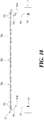
- FIG. 10 further illustrates the reflector 1.
- the signal distributing/combining apparatus 7 includes the circuit board 74 and the support plate 72.
- the circuit board 74 is configured to be formed on its upper surface with at least a signal distributing/combining conductor pattern 742 for carrying out high frequency signal distributing/combining operation.
- the support plate 72 made of a nonelastic, solid, metallic material, such as aluminum (alloy), is configured to have an upper mounting surface of a size corresponding to the circuit board 74, to mate with the circuit board 74 so that the underside of the circuit board 74 is in close contact with the upper mounting surface for supporting the circuit board 74, and to fixedly mate with the reflection plate 1 of the antenna device on the bottom side of the support plate 72.
- the signal distributing/combining apparatus may also be configured so that the upper side of the circuit board 74 is covered with a cap-shaped cover 76 made of a metal material (e.g., an aluminum alloy).
- the cover 76 may be configured to be coupled by screw fastening with the support plate 72.
- This can be understood to be a structure in which the support plate 72 and the cover 76 serve as an enclosure for enclosing the circuit board 74.
- Such provision of the cover 74 may further stabilize the signal processing function of the circuit board 74 while increasing the product size of the signal distributing/combining apparatus 7, and therefore it is appropriate to selectively determine whether or not to install the cover 74 depending on the design of the antenna device.
- the circuit board 74 of the signal distributing/combining apparatus 7 may be provided with a coupling conductor pattern 743 for generating a coupling signal in a non-contact coupling scheme with the signal distributing/combining conductor pattern 742.
- the coupling signal generated by the coupling conductor pattern 743 may be transmitted to the relevant device in order to confirm the quality of the signal transmitted from the corresponding signal distributing/combining conductor pattern 742.
- the circuit board 74 may be further provided, on its upper surface, with a ground conductor pattern 745 in a peripheral region adjacent to the signal distributing/combining conductor pattern 742 and the coupling conductor pattern 743.
- a large number of via holes reference numeral 7452 in FIG. 14 ) having fine diameters are formed at small intervals.
- a grounding layer may be formed on the lower surface of the circuit board 74 in the same way as the structure of the ordinary printed circuit board, and the above-mentioned numerous via holes electrically connect the ground conductor pattern 745 on the upper surface of the circuit board 74 with the grounding layer on the underside of the circuit board 74 to provide the grounding characteristics.
- the support plate 72 of the signal distributing/combining apparatus 7 is coupled to the circuit board 74 in a manner that it is in close contact with the lower surface of the circuit board 74, and some embodiments of the present disclosure feature a soldering method for bonding the underside of the circuit board 74 and the upper mounting surface of the support plate 72 for mounting the circuit board 74.
- the circuit board 74 may be printed with a solder cream where it is joined to the support plate 72, and the circuit board 74 printed with the solder cream may be mounted on the mounting surface of the support plate 72, and thereafter the solder cream may be melted and cured with a reflow soldering method within a high heat furnace.
- the support plate 72 may have some areas removed to form a plurality of open areas (indicated by A in FIG. 3 ) as appropriate.
- the open areas formed in the supporting plate 72 forms air passages when the circuit board 74 is brought into close contact with the support plate 72 and is soldered, thereby increasing the efficiency of the soldering operation.
- the large number of via holes formed in the ground conductor pattern 745 of the circuit board 74 can also serve as air passages during soldering work of the circuit board 74 and the support plate 72.
- the grounding conductor pattern 745 of the circuit board 74 may be further formed with a plurality of via holes not only for use in improving the grounding characteristics but also for the purpose of increasing the soldering work efficiency.
- the open areas formed in the support plate 72 may be utilized also when a coaxial cable is desired to be connected to the lower side of the circuit board 74 as described later.
- the support plate 72 is also provided with a plurality of cable holders 722 for supporting and fixating coaxial cables for signal transmission.
- the multiple cable holders 722 each corresponds to the shape and diameter (including some clearance) of the outer conductor of the coaxial cable, in order to mount the coaxial cable in a manner that the outer conductor of the coaxial cable is embedded or placed, by having, for example, a U-shaped structure formed elongated longitudinally.
- a plurality of signal input/output sections of the signal distributing/combining conductor pattern 742 may be at least partially configured to be formed at one edge of the circuit board 74.
- the multiple cable holders 722 are formed in portions corresponding to the plurality of signal input/output portions of the signal distributing/combining conductor pattern 742.
- the portions where the cable holders 722 are formed are suitably designed in consideration of the thickness of the circuit board 74 or the like so that inner conductors of the coaxial cables fixed by the cable holders 722 are not spaced apart from the upper surface of the circuit board 74 but exactly aligned with the signal input/output portions of the signal distributing/combining conductor pattern 742.
- the cable holders 722 may be formed to protrude laterally from one side of the support plate 72, and the support plate 72 including such multiple cable holders 722 may be integrally formed, for example, through a die-casting process.
- soldering work is carried out at the contact portions between the cable holder 722 and the outer conductors of the coaxial cables and at the contact portions between the inner conductors of the coaxial cable and the conductor pattern of the circuit board 74 so that the support plate 72 and the coaxial cable are fixedly connected electrically and mechanically.
- This method of connecting the coaxial cable for signal transmission to the support plate 72 by utilizing the cable holders 722 enables accurate and uniform processing together with ease of work, and further enables the product after the processing to firmly maintain the connection state between the support plate 72 and the coaxial cables in the actual use environment. This can substantially suppress PIMD that can be generated in the connection part between the relevant signal distributing/combining apparatus and the coaxial cable.
- some of the signal input/output portions of the signal distributing/combining conductor pattern 742 and/or the coupling conductor pattern 743 on the circuit board 74 mounted on the support plate 72 may be formed to connect with the coaxial cable(s) via the underside of the circuit board 74.
- the corresponding coaxial cable is connected to the circuit board 74 on the underside of the support plate 72 through the open areas formed in the support plate 72.
- the pattern design may dictate some of the signal input/output portions of the conductor pattern to be formed on the circuit board 74 inwardly rather than peripherally of the circuit board 74.
- the relevant portions are formed with holes (reference numeral 748 in FIG. 5 ) for cable connection, and the inner conductor of the coaxial cable is inserted from the lower side of the circuit board 74 through the cable connecting hole into place so as to protrude above the circuit board 74.
- the support plate 72 may be further provided on its underside with a plurality of cable holders 729 for fixedly and/or supportively mount the coaxial cables connected to the underside of the circuit board 74.
- the multiple cable holders 729 each corresponds to the shape and diameter of the coaxial cable, in order to mount the coaxial cable in a manner that the outer conductor of the coaxial cable is embedded or placed, by having at least, for example, a U-shaped groove formed on the lower surface of the support plate 72.
- the support plate 72 has its lower part fixedly coupled with the reflection plate 1 of the antenna device.
- the lower side of the support plate 72 is formed with multiple fastening protrusions 724 respectively provided with screw fastening recesses 7242.
- the multiple fastening protrusions 724 may be provided respectively at portions corresponding to the underside corners of the support plate 72 having, for example, a rectangular shape and they may protrude to an appropriate height at which the support plate 72 contacts the reflection plate 1 by the multiple fastening protrusions 724.
- the reflection plate 1 has a plurality of screw insertion holes 102 formed respectively at positions corresponding to the portions contacted by the multiple fastening protrusions 724.
- Fastening screws (reference numeral 112 in FIG. 10 ) are threaded through the plurality of screw insertion holes 102 into the screw fastening recesses 7242 of the multiple fastening protrusions 724, whereby the support plate 72 is fixed to the reflection plate 1. This way of coupling the support plate 72 with the reflection plate 1 may minimize the contact area between the two elements, which in turn mitigates unstable factor of the ground contact.
- the support plate 72 may be provided with additional structures for other functions such as facilitating the coupling operation with the circuit board 74 and securing the coupled state.
- a guardrail member 725 may be formed on the support plate 72 so as to surround at least a part of a mounting surface on which the circuit board 74 is mounted.
- the support plate 72 may be formed, on the mounting surface for the circuit board 74, with one or more coupling protrusion members 726, and in correspondence therewith, the circuit board 74 may have one or more coupling holes 749 to be coupled with the coupling protrusion members 726 in such a manner that the coupling projection members 726 are inserted.
- one or more partition members 728 may be formed in an appropriate length, and in correspondence therewith, the circuit board 74 may have one or more slots 747 to be coupled with the partition members 728 in such a manner that the partition members 728 are inserted.
- the partition member 728 formed on the support plate 72 is configured to function not only to facilitate the coupling operation and maintain a stable coupling state between the support plate 72 and the circuit board 74 but also to prevent signal leakage or interference of signals between the conductor patterns formed on the circuit board 74.
- the partition member 728 is formed so as to protrude from the upper surface of the circuit board 74 on which the conductor pattern is formed to a preset height. This provides electrically grounded vertical barrier walls of the partition member 728 to its opposite side conductor patterns on the circuit board 74. Multiples of such partition member 728 minimize signal leakage or signal interference between the conductor patterns with their partition member 728 interposed.
- the antenna device may have a multi-band service structure wherein the signal/distribution coupling conductor pattern 742 is formed with distinguishable conductor patterns for signal distributing/combining for each band.
- the partition member 728 may formed to be positioned between the conductor patterns for band-specific signal distributing/combining so as to prevent band-specific signal leakage and signal interference.
- FIGS. 12A and 12B are illustrations showing a connection structure between the signal distributing/combining apparatus 7 and the coaxial cable 22 in FIG. 2 , whereby the coaxial cable 22 is connected to the cable holder 722 on the upper portion of the signal distributing/combining apparatus 7.
- the signal distributing/combining apparatus 7 and the coaxial cable 22 are shown before and after their interconnection in FIGS. 12A and 12B , respectively.
- the coaxial cable 22 is coupled to the cable holder 722 with its insulating and protective sheath 222 and the outer conductor 224 removed so that certain portions of the grounding outer conductor 224 and the signal transmission inner conductor 226 are exposed.
- the external conductor 224 of the coaxial cable 22 is inserted firmly in the cable holder 722 so that the coaxial cable 22 is fixed by the cable holder 722 with the inner conductor 226 contacting the signal input/output section of the signal distributing/combining conductor pattern 742. Thereafter, as shown in the dot-dash line circles A of FIG. 12B , soldering work is performed on the contact portion between the cable holder 722 and the external conductor 224 of the coaxial cable 22 and on the connection portion of the internal conductor 226 of the coaxial cable 22 and the signal distributing/combining conductor pattern 742.
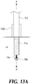
- FIGS. 13A , 13B and 13C are exemplary views of another connection structure between the signal distributing/combining apparatus of FIG. 2 and a coaxial cable, wherein a coaxial cable 71 is coupled to the cable holder 729 on the underside of the signal distributing/combining apparatus 7.
- FIG. 13A is an elevation view showing that the coaxial cable 71 is connected to the cable holder 729
- FIGS. 13B and 13C are cross-sectional views taken along line A-A' in FIG. 13A
- FIG. 13B shows the apparatus with the coaxial cable 71 removed to facilitate understanding.
- the coaxial cable 71 is coupled to the cable holder 729 with its sheath 712 and outer conductor 714 partially removed so that certain portions of the outer conductor 714 and an inner conductor 716 are exposed.
- the cable holder 729 may be formed to have a guard member 7292 structured for clamping that coaxial cable 71 by its side.
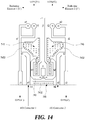
- FIG. 14 is an enlarged view of a partial circuit pattern of the circuit board 74 of the signal distributing/combining apparatus 7 in FIG. 2 , and shows, for example, the corresponding circuit pattern indicated by part A in FIG. 6 .
- the corresponding circuit pattern may be a circuit configuration for combining/distributing signals of a single band in a multiband service structure.
- FIG. 14 the configurations of the signal distributing/combining conductor pattern and the coupling conductor pattern of the circuit board 74 will be described in more detail.
- a signal for example, a transmit signal
- I/O connector 1 a first input/output connector
- a pattern a1 which is a first input terminal 'in1'
- the input signal at pattern a1 is subsequently distributed from patterns b1 and d1 to a downward or lower phase shifter D/PS #1, a 0 degree phase-shift radiating element 1 (i.e., with no phase shift) and an upward or upper phase shifter U/PS #1.
- the signal for distribution to the lower phase shifter D/PS #1 is provided to a pattern c1
- the signal for distribution to the radiating element 1 is provided to a pattern e1
- the signal for distribution to the upper phase shifter U/PS #1 is provided to a pattern f1.
- the radiating elements in a single service band are arranged in a row in the vertical direction, and for vertical steering adjustment, the radiating elements in the normally vertical arrangement are relatively phase shifted based on their positions in the arrangement.
- the radiating elements positioned on the upper side with respect to the centrally positioned radiating element are phase shifted through the aforementioned upper phase shifter by a positive [+] angle to have respective phase differences
- the radiating elements positioned thereunder are phase shifted through the aforementioned lower phase shifter by a negative [-] angle to have the respective mutual phase differences.
- the signal distributing/combining conductor pattern as described above may appropriately distribute the signal input by one input/output connector (I/O connector 1) and transfer the signal via the pattern c1 to the lower phase shifter D/PS #1, via the pattern e1 to the radiating element with no phase shift, and via the pattern f1 to the upper phase shifter U/PS #1.
- Detailed structures such as the shapes and lengths of the patterns a1 to f1 are appropriately designed in consideration of the phase, mutual impedance and others of the signals to be distributed and transferred.
- a signal provided from a second input/output connector (I/O connector 2) through the coaxial cable is input to a pattern a2 which is a second input terminal 'in2', and the input signal at pattern a2 is subsequently distributed from patterns b2 and d2 for further subsequent distribution via patterns c2, f2 and e2 to a lower phase shifter D/PS #2, a 0 degree phase-shift radiating element 2 (i.e., with no phase shift) and an upper phase shifter U/PS #2, respectively.
- the patterns for processing the signal input at the first input/output connector are the signal processing pattern for generating a polarized wave of +45 degree
- the patterns for processing the signal input at the second input/output connector are the signal processing pattern for generating a polarized wave of -45 degree.
- the above signal distributing/combining conductor pattern has been described by exemplifying the function of distributing transmit signals, but it can be understood that this pattern can do the reverse as well for performing to combine and provide the receive signals to the I/O connector side.
- the signal distributing/combining conductor pattern in FIG. 14 corresponds to the structure of 2T2R (2 Tx 2 Rx) in an antenna device
- the whole signal distributing/combining conductor pattern shown in FIG. 2 et al. has a structure generally corresponding to the 8T8R structure.
- the coupling conductor pattern includes an h1 pattern and an h2 pattern for coupling the transmission signal by the pattern a1 and the transmission signal of the pattern a2 in the signal distributing/combining conductor pattern, respectively.
- the signals coupled by the patterns h1 and h2 are then combined by a pattern i1 and transmitted to a pattern j1.
- the signal delivered to the pattern j1 is then transmitted to the relevant device (or externally) to analyze the transmitted signal to determine the quality of the signals (e.g., transmit signals) transferred from the patterns a1 and a2.
- checking the quality of the signals may be performed by distinguishably setting the respective transmission periods of the transmit signals transferred from the pattern a1 and the pattern a2.
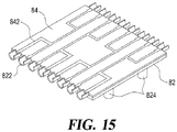
- FIG. 15 is a perspective view of a signal distributing/combining apparatus according to another embodiment of the present disclosure.
- FIGS. 16 and 17 are respectively a plan view and a rear view of the signal distributing/combining apparatus of FIG. 15 .
- the signal distributing/combining apparatus 7 according to another embodiment is similar to the structure according to the embodiment shown in FIG. 2 et al. in that it has a circuit board 84 on which a signal distributing/combining conductor pattern 842 is formed for high frequency signal distributing/combining, and a support plate 82.
- the support plate 82 is configured to have an upper mounting surface of a size corresponding to the circuit board 84, to mate with the circuit board 84 so that the underside of the circuit board 84 is in close contact with the upper mounting surface for supporting the circuit board 84, and to fixedly mate with the reflection plate of the antenna device on the bottom side of the support plate 82.
- the circuit board 74 according to another embodiment in FIGS. 15 to 17 is not formed with a coupling conductor pattern (743 in FIG. 3 ) and a ground conductor pattern (745 in FIG. 3 ).
- the structure of another embodiment as described above may be made similar to that of the embodiment shown in FIG. 2 etc.
- the support plate 82 may be provided with a plurality of cable holders 822 for supporting and fixating coaxial cables for signal transmission, a plurality of fastening portions 824 for coupling with the reflection plate and some areas removed to form open areas.
- the configurations and operations of the signal distributing/combining apparatuses of the present disclosure in an antenna device of the mobile communication base station may be achieved according to some embodiments which are particularized for illustration, but it is to be understood that other variations may be made without departing from the scope of the disclosure.
- the signal distributing/combining apparatuses are disposed centrally of the reflection plate and connected via the coaxial cable to the input/output connector, upper and lower phase shifters, and others, although the signal distributing/combining apparatuses connected via the coaxial cable to various other devices. Further, the signal distributing/combining apparatuses may be properly installed in other parts than the central portion of the reflection plate.
- the signal distributing/combining conductor pattern of the signal distributing/combining apparatus has been explained by way of example, that it corresponds to the 8T8R structure as a whole, but in addition to this, the present disclosure may also be applied to 4T4R or any other structures.
Landscapes
- Engineering & Computer Science (AREA)
- Computer Networks & Wireless Communication (AREA)
- Physics & Mathematics (AREA)
- Electromagnetism (AREA)
- Variable-Direction Aerials And Aerial Arrays (AREA)
- Details Of Aerials (AREA)
Abstract
Description
- In some embodiments, the present disclosure relates to an antenna device applicable to a base station and a relay station in a mobile communication (PCS, cellular, CDMA, GSM, LTE, etc.) network. More particularly, the present disclosure in some embodiments relates to a signal distributing/combining apparatus for distributing or combining radio frequency (RF) signals in an antenna device.
- Generally, a base station or a relay station (hereinafter collectively referred to as "base station") of a mobile communication system has been divided into a base station main unit configured to process transmit and receive signals and an antenna device including a plurality of radiating elements for transmitting/receiving radio signals. The base station main unit is usually installed at a low position on the ground, and the antenna device is installed at a high position such as a building roof or a tower, and the base station main unit and the antenna device may be connected to each other through a feeding cable or the like.
- The antenna device of the base station includes a plurality of radiating elements for transmitting/receiving high frequency radio signals. At this time, the radiating elements are installed on one surface (for example, the front surface) of a metal reflecting plate having a relatively large area. Further, the antenna device is provided with various circuits or devices for processing signals transmitted and received via the plurality of radiating elements, and, for example, the circuits or devices may be fixedly installed on the back face of the reflecting plate. Such devices may include a phase shifter for adjusting the phase of the signals of the multiple radiating elements, and an apparatus for distributing/combining the transmit and receive signals of the internal devices and the radiating elements. At this time, the respective devices may be connected via a signal transmission line, and a substantial portion of which is formed of coaxial cable.
- Meanwhile, in the antenna device of such a structure, it is a serious matter, in addition to having the required transmission/reception properties of the signal for the band, to suppress PIMD (Passive Intermodulation Distortion) generated by discontinuous contact surfaces, unstable connection state or other causes in the respective device structure itself and at the connections between devices.
- In this case, the antenna device almost invariably requires a signal distributing/combining apparatus and the structure for making connections through soldering a coaxial cable to that signal distributing/combining apparatus, which in turn requires effective measures to suppress PIMD that can be generated due to unstable connection state occurring at the connections between the signal distributing/combining apparatus and the coaxial cable or due to nonuniform soldering state, etc.
- Therefore, in some embodiments, the present disclosure seeks to provide a signal distributing/combining apparatus in a mobile communication base station antenna apparatus, which is capable of suppressing the PIMD generated at the connection with the coaxial cable, stabilizing the quality of soldering at the connection, and stabilizing the grounding quality of the apparatus.
- In accordance with some embodiments of the present disclosure, a signal distributing/combining apparatus in an antenna device of a mobile communication base station includes a circuit board and a support plate. The circuit board is configured to have an upper surface formed with a signal distributing/combining conductor pattern for a high frequency signal distributing/combining operation. The support plate is configured to have an upper mounting surface of a size corresponding to the circuit board, to mate with the circuit board so that an underside of the circuit board is in close contact with the upper mounting surface for supporting the circuit board, and to fixedly mate with the antenna device at a reflection plate on a bottom side of the support plate. Here, the support plate is provided with a plurality of cable holders for supporting and fixating coaxial cables for signal transmission, which are connected from outside of the signal distributing/combining apparatus, the signal distributing/combining conductor pattern is formed with a plurality of signal input/output portions. The plurality of cable holders is formed on the signal distributing/combining conductor pattern at portions corresponding to at least some of a plurality of signal input/output portions, the cable holders having a structure formed elongated longitudinally and corresponding to outer conductors of the coaxial cables in order to mount the coaxial cable by inserting the outer conductors.
- The cable holders may be formed at predetermined positions in the support plate such that inner conductors of the coaxial cables are placed in contact with the upper surface of the circuit board.
- The underside of the circuit board and the upper mounting surface of the support plate for mounting the circuit board may be bonded together with a solder cream which is melted and cured with a reflow soldering method.
- The upper surface of the circuit board may be formed with a coupling conductor pattern for generating a coupling signal in a non-contact coupling scheme with the signal distributing/combining conductor pattern.
- The upper surface of the circuit board may be formed with a ground conductor pattern in a peripheral region adjacent to the signal distributing/combining conductor pattern and the coupling conductor pattern, and the ground conductor pattern may have a plurality of via holes for making an electrical connection with grounding layer on the underside of the circuit board.
- The support plate may have open areas, and include a plurality of cable holders corresponding respectively to the coaxial cables for mounting the coaxial cables connected to the underside of the circuit board after passing through the open areas.
- The support plate may include multiple fastening protrusions which protrude downwardly of the support plate and are respectively formed with screw fastening recesses for screw fastening with a reflection plate of the antenna device.
- The support plate may include a mounting surface configured to mount the circuit board and to have one or more partition members formed in a predetermined length and a predetermined height. The circuit board may have one or more slots to be coupled with the partition members in such a manner that the partition members are inserted. And the partition members may be formed so as to protrude from the upper surface of the circuit board on which the conductor pattern is formed to a preset height.
- As described above, the signal distributing/combining apparatus in the mobile communication base station antenna device according to at least one embodiment of the present disclosure can suppress the PIMD generated at the connection with the cable, stabilize the quality of the soldering at the connection, and stabilize the grounding quality of the apparatus.
-
-
FIG. 1 is a structure of an antenna device of a mobile communication base station to which a signal distributing/combining apparatus according to at least one embodiment of the present disclosure is applied. -
FIG. 2 is a perspective view of a signal distributing/combining apparatus according to at least one embodiment of the present disclosure. -
FIG. 3 is an exploded perspective view of a circuit board and a support plate of the signal distributing/combining apparatus ofFIG. 2 . -
FIG. 4 is a plan view of the signal distributing/combining apparatus ofFIG. 2 . -
FIG. 5 is a rear view of the signal distributing/combining apparatus ofFIG. 2 . -
FIG. 6 is a plan view of the circuit board of the signal distributing/combining apparatus ofFIG. 2 . -
FIG. 7 is a rear view of the circuit board of the signal distributing/combining apparatus ofFIG. 2 . -
FIG. 8 is a plan view of the support plate of the signal distributing/combining apparatus ofFIG. 2 . -
FIG. 9 is a rear view of the support plate of the signal distributing/combining apparatus ofFIG. 2 . -
FIG. 10 is a first side view of the support plate of the signal distributing/combining apparatus ofFIG. 2 . -
FIG. 11 is a second side view of the support plate of the signal distributing/combining apparatus ofFIG. 2 . -
FIGS. 12A andFIG. 12B are exemplary views of a connection structure between the signal distributing/combining apparatus ofFIG. 2 and a coaxial cable. -
FIGS. 13A ,13B and13C are exemplary views of another connection structure between the signal distributing/combining apparatus ofFIG. 2 and a coaxial cable. -
FIG. 14 is an enlarged view of a partial circuit pattern of the circuit board of the signal distributing/combining apparatus ofFIG. 2 . -
FIG. 15 is a perspective view of a signal distributing/combining apparatus according to another embodiment of the present disclosure. -
FIG. 16 is a plan view of the signal distributing/combining apparatus ofFIG. 15 . -
FIG. 17 is a rear view of the signal distributing/combining apparatus ofFIG. 15 . - Hereinafter, at least one embodiment of the present disclosure will be described in detail with reference to the accompanying drawings. In the following description, specific details such as specific components are disclosed, which are provided only for a better understanding of the present disclosure. It will be apparent to those skilled in the art that various modifications and variations can be made in the present disclosure without departing from the idea or the scope of the disclosure. In the following description, like reference numerals designate like elements as possible, although the elements are shown in different drawings, wherein some reference numerals are refrained from being shown to avoid excessively complicating the drawings.
-
FIG. 1 is a schematic of a structure of a mobile communication base station antenna device to which a signal distributing/combining apparatus according to at least one embodiment of the present disclosure is applied. Referring toFIG. 1 , the base station antenna device is configured as a metal plate having a relatively large area as a whole, and includes areflection plate 1, anupper phase shifter 6, alower phase shifter 5, a radome 4, alower cap 2 and an upper cap 3. Thereflection plate 1 has one side (e.g., the front side) mounted with a plurality of radiating elements (not shown) for transmitting/receiving radio signals. The upper andlower phase shifters reflection plate 1, and adjust the phases of the signals of the multiple radiation elements. The radome 4 is formed in an integrated cylindrical shape to surround interior devices of the antenna including thereflection plate 1 and the upper andlower phase shifters lower cap 2 and the upper cap 3 fixate upper and lower portions of the reflectingplate 1 respectively, and sealingly join with the upper and lower open portions of the cylindrical radome 4. - Further, a signal distributing/combining
apparatus 7 according to at least one embodiment of the present disclosure may be provided, for example, in a central portion on the back surface of thereflection plate 1 of the antenna device. For example, the signal distributing/combiningapparatus 7 receives transmitted signals input from the base station's main unit device (not shown) outside the antenna device and distributes the input signals to the antenna's interior devices including the upper andlower phase shifters - In addition, the radome 4 of the antenna device may be provided with other additional distributing/combining circuits, or amplifiers, filters, etc. and it may be appropriately installed with various electronic components (not shown) such as a detection circuit for detecting various operational states of the antenna including signal transmission quality and a main control device (e.g., an MCU etc.) for controlling the overall operation. However, for convenience of explanation, illustration of these electronic components is omitted in
FIG. 1 . - Meanwhile, as shown in
FIG. 1 , thelower cap 2 is usually installed with a plurality of input/output connectors 202 for inputting/outputting transmit/receive signals to and from the antenna device. The input/output connectors 202 may be directly or indirectly connected to the base station main unit side via a plurality ofpower supply cables 8. Inside the antenna device, a plurality ofcoaxial cables 22 may be used as signal transmission transmission lines between the input/output connectors 202 of thelower cap 2 and the signal distributing/combiningapparatus 7. In addition, the signal distributing/combiningapparatus 7 may be connected with the upper andlower phase shifters coaxial cables -
FIG. 1 illustrates the upper andlower phase thousands - On the other hand, the signal distributing/combining
apparatus 7 may be mainly provided with a printed circuit board on which a conductor pattern is formed for high frequency signal distributing/combining. When connecting a coaxial cable to a printed circuit board, it is typical to apply a method of soldering the inner conductor of the coaxial cable to the input/output end of the conductor pattern. Likewise, when connecting the coaxial cable to the signal distributing/combiningapparatus 7, the interconnection is also made by a soldering method, but in this case, the signal distributing/combiningapparatus 7 according to some embodiments, as will be described later, provides a structure capable of suppressing the occurrence of PIMD, particularly at the connecting portion of the coaxial cable. -
FIG. 2 is a perspective view of the signal distributing/combiningapparatus 7 according to at least one embodiment of the present disclosure, further illustrating thereflector 1.FIG. 3 is an exploded perspective view of acircuit board 74 and asupport plate 72 of the signal distributing/combiningapparatus 7 ofFIG. 2 .FIGS. 4 and5 are respectively a plan view and a rear view of the signal distributing/combiningapparatus 7 ofFIG. 2 .FIGS. 6 and7 are respectively a plan view and a rear view of thecircuit board 74 of the signal distributing/combiningapparatus 7 ofFIG. 2 .FIGS. 8 to 11 are respectively a plan view, a rear view, a first side view and a second side view of thesupport plate 72 of the signal distributing/combiningapparatus 7 ofFIG. 2 . In particular,FIG. 10 , further illustrates thereflector 1. - Referring to
FIGS. 2 to 11 , the signal distributing/combiningapparatus 7 according to at least one embodiment of the present disclosure includes thecircuit board 74 and thesupport plate 72. Thecircuit board 74 is configured to be formed on its upper surface with at least a signal distributing/combiningconductor pattern 742 for carrying out high frequency signal distributing/combining operation. Thesupport plate 72, made of a nonelastic, solid, metallic material, such as aluminum (alloy), is configured to have an upper mounting surface of a size corresponding to thecircuit board 74, to mate with thecircuit board 74 so that the underside of thecircuit board 74 is in close contact with the upper mounting surface for supporting thecircuit board 74, and to fixedly mate with thereflection plate 1 of the antenna device on the bottom side of thesupport plate 72. - As indicated by a dotted box in
FIG. 2 , in some cases, the signal distributing/combining apparatus may also be configured so that the upper side of thecircuit board 74 is covered with a cap-shapedcover 76 made of a metal material (e.g., an aluminum alloy). Thecover 76 may be configured to be coupled by screw fastening with thesupport plate 72. This can be understood to be a structure in which thesupport plate 72 and thecover 76 serve as an enclosure for enclosing thecircuit board 74. Such provision of thecover 74 may further stabilize the signal processing function of thecircuit board 74 while increasing the product size of the signal distributing/combiningapparatus 7, and therefore it is appropriate to selectively determine whether or not to install thecover 74 depending on the design of the antenna device. - In addition to the signal distributing/combining
conductor pattern 742, thecircuit board 74 of the signal distributing/combiningapparatus 7 may be provided with acoupling conductor pattern 743 for generating a coupling signal in a non-contact coupling scheme with the signal distributing/combiningconductor pattern 742. The coupling signal generated by thecoupling conductor pattern 743 may be transmitted to the relevant device in order to confirm the quality of the signal transmitted from the corresponding signal distributing/combiningconductor pattern 742. - In order to improve the grounding characteristics of the signal distributing/combining
conductor pattern 742 and thecoupling conductor pattern 743, thecircuit board 74 may be further provided, on its upper surface, with aground conductor pattern 745 in a peripheral region adjacent to the signal distributing/combiningconductor pattern 742 and thecoupling conductor pattern 743. In theground conductor pattern 745, particularly at its edge portion, a large number of via holes (reference numeral 7452 inFIG. 14 ) having fine diameters are formed at small intervals. A grounding layer may be formed on the lower surface of thecircuit board 74 in the same way as the structure of the ordinary printed circuit board, and the above-mentioned numerous via holes electrically connect theground conductor pattern 745 on the upper surface of thecircuit board 74 with the grounding layer on the underside of thecircuit board 74 to provide the grounding characteristics. - The
support plate 72 of the signal distributing/combiningapparatus 7 is coupled to thecircuit board 74 in a manner that it is in close contact with the lower surface of thecircuit board 74, and some embodiments of the present disclosure feature a soldering method for bonding the underside of thecircuit board 74 and the upper mounting surface of thesupport plate 72 for mounting thecircuit board 74. For example, thecircuit board 74 may be printed with a solder cream where it is joined to thesupport plate 72, and thecircuit board 74 printed with the solder cream may be mounted on the mounting surface of thesupport plate 72, and thereafter the solder cream may be melted and cured with a reflow soldering method within a high heat furnace. At this time, depending on the material of thesupport plate 72, in order to enable the soldering operation on thesupport plate 72 or to improve the quality of soldering, corresponding portions to the solder cream may undergo a plating treatment in advance with a material such as tin. In this way, joining by thecircuit board 74 and thesupport plate 72 by using the reflow soldering method can remarkably stabilize the ground contact quality of thecircuit board 74 and thesupport plate 72. - Further, the
support plate 72 may have some areas removed to form a plurality of open areas (indicated by A inFIG. 3 ) as appropriate. The open areas formed in the supportingplate 72 forms air passages when thecircuit board 74 is brought into close contact with thesupport plate 72 and is soldered, thereby increasing the efficiency of the soldering operation. Similarly, the large number of via holes formed in theground conductor pattern 745 of thecircuit board 74 can also serve as air passages during soldering work of thecircuit board 74 and thesupport plate 72. For this reason, thegrounding conductor pattern 745 of thecircuit board 74 may be further formed with a plurality of via holes not only for use in improving the grounding characteristics but also for the purpose of increasing the soldering work efficiency. On the other hand, the open areas formed in thesupport plate 72 may be utilized also when a coaxial cable is desired to be connected to the lower side of thecircuit board 74 as described later. - The
support plate 72 is also provided with a plurality ofcable holders 722 for supporting and fixating coaxial cables for signal transmission. Themultiple cable holders 722 each corresponds to the shape and diameter (including some clearance) of the outer conductor of the coaxial cable, in order to mount the coaxial cable in a manner that the outer conductor of the coaxial cable is embedded or placed, by having, for example, a U-shaped structure formed elongated longitudinally. - In the
circuit board 74 mounted on thesupport plate 72, a plurality of signal input/output sections of the signal distributing/combiningconductor pattern 742, that is, its areas to be connected with the coaxial cable may be at least partially configured to be formed at one edge of thecircuit board 74. To this end, themultiple cable holders 722 are formed in portions corresponding to the plurality of signal input/output portions of the signal distributing/combiningconductor pattern 742. Further, the portions where thecable holders 722 are formed are suitably designed in consideration of the thickness of thecircuit board 74 or the like so that inner conductors of the coaxial cables fixed by thecable holders 722 are not spaced apart from the upper surface of thecircuit board 74 but exactly aligned with the signal input/output portions of the signal distributing/combiningconductor pattern 742. - The
cable holders 722 may be formed to protrude laterally from one side of thesupport plate 72, and thesupport plate 72 including suchmultiple cable holders 722 may be integrally formed, for example, through a die-casting process. - Once the coaxial cables are attached to the
cable holders 722 having such a configuration, soldering work is carried out at the contact portions between thecable holder 722 and the outer conductors of the coaxial cables and at the contact portions between the inner conductors of the coaxial cable and the conductor pattern of thecircuit board 74 so that thesupport plate 72 and the coaxial cable are fixedly connected electrically and mechanically. This method of connecting the coaxial cable for signal transmission to thesupport plate 72 by utilizing thecable holders 722 enables accurate and uniform processing together with ease of work, and further enables the product after the processing to firmly maintain the connection state between thesupport plate 72 and the coaxial cables in the actual use environment. This can substantially suppress PIMD that can be generated in the connection part between the relevant signal distributing/combining apparatus and the coaxial cable. - Meanwhile, some of the signal input/output portions of the signal distributing/combining
conductor pattern 742 and/or thecoupling conductor pattern 743 on thecircuit board 74 mounted on thesupport plate 72 may be formed to connect with the coaxial cable(s) via the underside of thecircuit board 74. In that case, the corresponding coaxial cable is connected to thecircuit board 74 on the underside of thesupport plate 72 through the open areas formed in thesupport plate 72. In other words, the pattern design may dictate some of the signal input/output portions of the conductor pattern to be formed on thecircuit board 74 inwardly rather than peripherally of thecircuit board 74. In that case, the relevant portions are formed with holes (reference numeral 748 inFIG. 5 ) for cable connection, and the inner conductor of the coaxial cable is inserted from the lower side of thecircuit board 74 through the cable connecting hole into place so as to protrude above thecircuit board 74. - The
support plate 72 may be further provided on its underside with a plurality ofcable holders 729 for fixedly and/or supportively mount the coaxial cables connected to the underside of thecircuit board 74. Themultiple cable holders 729 each corresponds to the shape and diameter of the coaxial cable, in order to mount the coaxial cable in a manner that the outer conductor of the coaxial cable is embedded or placed, by having at least, for example, a U-shaped groove formed on the lower surface of thesupport plate 72. - Further, as shown in
FIGS. 1 and10 in more detail, thesupport plate 72 has its lower part fixedly coupled with thereflection plate 1 of the antenna device. For this purpose, the lower side of thesupport plate 72 is formed withmultiple fastening protrusions 724 respectively provided with screw fastening recesses 7242. Themultiple fastening protrusions 724 may be provided respectively at portions corresponding to the underside corners of thesupport plate 72 having, for example, a rectangular shape and they may protrude to an appropriate height at which thesupport plate 72 contacts thereflection plate 1 by themultiple fastening protrusions 724. Thereflection plate 1 has a plurality of screw insertion holes 102 formed respectively at positions corresponding to the portions contacted by themultiple fastening protrusions 724. Fastening screws (reference numeral 112 inFIG. 10 ) are threaded through the plurality of screw insertion holes 102 into thescrew fastening recesses 7242 of themultiple fastening protrusions 724, whereby thesupport plate 72 is fixed to thereflection plate 1. This way of coupling thesupport plate 72 with thereflection plate 1 may minimize the contact area between the two elements, which in turn mitigates unstable factor of the ground contact. - The
support plate 72 may be provided with additional structures for other functions such as facilitating the coupling operation with thecircuit board 74 and securing the coupled state. For example, aguardrail member 725 may be formed on thesupport plate 72 so as to surround at least a part of a mounting surface on which thecircuit board 74 is mounted. In addition, thesupport plate 72 may be formed, on the mounting surface for thecircuit board 74, with one or morecoupling protrusion members 726, and in correspondence therewith, thecircuit board 74 may have one ormore coupling holes 749 to be coupled with thecoupling protrusion members 726 in such a manner that thecoupling projection members 726 are inserted. Further, in thesupport plate 72, one ormore partition members 728 may be formed in an appropriate length, and in correspondence therewith, thecircuit board 74 may have one ormore slots 747 to be coupled with thepartition members 728 in such a manner that thepartition members 728 are inserted. - The
partition member 728 formed on thesupport plate 72 is configured to function not only to facilitate the coupling operation and maintain a stable coupling state between thesupport plate 72 and thecircuit board 74 but also to prevent signal leakage or interference of signals between the conductor patterns formed on thecircuit board 74. For example, thepartition member 728 is formed so as to protrude from the upper surface of thecircuit board 74 on which the conductor pattern is formed to a preset height. This provides electrically grounded vertical barrier walls of thepartition member 728 to its opposite side conductor patterns on thecircuit board 74. Multiples ofsuch partition member 728 minimize signal leakage or signal interference between the conductor patterns with theirpartition member 728 interposed. - For example, the antenna device may have a multi-band service structure wherein the signal/distribution
coupling conductor pattern 742 is formed with distinguishable conductor patterns for signal distributing/combining for each band. In such a structure, thepartition member 728 may formed to be positioned between the conductor patterns for band-specific signal distributing/combining so as to prevent band-specific signal leakage and signal interference. -
FIGS. 12A and12B are illustrations showing a connection structure between the signal distributing/combiningapparatus 7 and thecoaxial cable 22 inFIG. 2 , whereby thecoaxial cable 22 is connected to thecable holder 722 on the upper portion of the signal distributing/combiningapparatus 7. At this time, the signal distributing/combiningapparatus 7 and thecoaxial cable 22 are shown before and after their interconnection inFIGS. 12A and12B , respectively. As illustrated, thecoaxial cable 22 is coupled to thecable holder 722 with its insulating andprotective sheath 222 and theouter conductor 224 removed so that certain portions of the groundingouter conductor 224 and the signal transmissioninner conductor 226 are exposed. - At this time, the
external conductor 224 of thecoaxial cable 22 is inserted firmly in thecable holder 722 so that thecoaxial cable 22 is fixed by thecable holder 722 with theinner conductor 226 contacting the signal input/output section of the signal distributing/combiningconductor pattern 742. Thereafter, as shown in the dot-dash line circles A ofFIG. 12B , soldering work is performed on the contact portion between thecable holder 722 and theexternal conductor 224 of thecoaxial cable 22 and on the connection portion of theinternal conductor 226 of thecoaxial cable 22 and the signal distributing/combiningconductor pattern 742. -
FIGS. 13A ,13B and13C are exemplary views of another connection structure between the signal distributing/combining apparatus ofFIG. 2 and a coaxial cable, wherein acoaxial cable 71 is coupled to thecable holder 729 on the underside of the signal distributing/combiningapparatus 7. At this time,FIG. 13A is an elevation view showing that thecoaxial cable 71 is connected to thecable holder 729, andFIGS. 13B and13C are cross-sectional views taken along line A-A' inFIG. 13A .FIG. 13B shows the apparatus with thecoaxial cable 71 removed to facilitate understanding. AsFIGS. 13A to 13C illustrate, thecoaxial cable 71 is coupled to thecable holder 729 with itssheath 712 andouter conductor 714 partially removed so that certain portions of theouter conductor 714 and aninner conductor 716 are exposed. - At this time, a part of the covering 712 of the
coaxial cable 71 is inserted or placed in thecable holder 729 so that thecoaxial cable 71 is fixed by thecable holder 729 with theouter conductor 714 contacting the ground layer on the underside of thecircuit board 74. Theinner conductor 716 of thecoaxial cable 71 is installed by inserting into acable connection hole 748 formed in thecircuit board 74. On the other hand, to better secure thecoaxial cable 71 held in thecable holder 729, thecable holder 729 may be formed to have aguard member 7292 structured for clamping thatcoaxial cable 71 by its side. -
FIG. 14 is an enlarged view of a partial circuit pattern of thecircuit board 74 of the signal distributing/combiningapparatus 7 inFIG. 2 , and shows, for example, the corresponding circuit pattern indicated by part A inFIG. 6 . The corresponding circuit pattern may be a circuit configuration for combining/distributing signals of a single band in a multiband service structure. With reference toFIG. 14 , the configurations of the signal distributing/combining conductor pattern and the coupling conductor pattern of thecircuit board 74 will be described in more detail. - First, a signal distributing/combining conductor pattern will be described. For example, a signal (for example, a transmit signal) provided from a first input/output connector (I/O connector 1) through the coaxial cable is input to a pattern a1 which is a first input terminal 'in1', and the input signal at pattern a1 is subsequently distributed from patterns b1 and d1 to a downward or lower phase shifter D/
PS # 1, a 0 degree phase-shift radiating element 1 (i.e., with no phase shift) and an upward or upper phase shifter U/PS # 1. The signal for distribution to the lower phase shifter D/PS # 1 is provided to a pattern c1, the signal for distribution to theradiating element 1 is provided to a pattern e1, and the signal for distribution to the upper phase shifter U/PS # 1 is provided to a pattern f1. - In ordinary antenna devices, the radiating elements in a single service band are arranged in a row in the vertical direction, and for vertical steering adjustment, the radiating elements in the normally vertical arrangement are relatively phase shifted based on their positions in the arrangement. In the antenna having such a structure, for example, the radiating elements positioned on the upper side with respect to the centrally positioned radiating element (radiating element with no phase shift) are phase shifted through the aforementioned upper phase shifter by a positive [+] angle to have respective phase differences, and the radiating elements positioned thereunder are phase shifted through the aforementioned lower phase shifter by a negative [-] angle to have the respective mutual phase differences.
- In concert with this arrangement, the signal distributing/combining conductor pattern as described above may appropriately distribute the signal input by one input/output connector (I/O connector 1) and transfer the signal via the pattern c1 to the lower phase shifter D/
PS # 1, via the pattern e1 to the radiating element with no phase shift, and via the pattern f1 to the upper phase shifter U/PS # 1. Detailed structures such as the shapes and lengths of the patterns a1 to f1 are appropriately designed in consideration of the phase, mutual impedance and others of the signals to be distributed and transferred. - On the other hand, a signal provided from a second input/output connector (I/O connector 2) through the coaxial cable is input to a pattern a2 which is a second input terminal 'in2', and the input signal at pattern a2 is subsequently distributed from patterns b2 and d2 for further subsequent distribution via patterns c2, f2 and e2 to a lower phase shifter D/
PS # 2, a 0 degree phase-shift radiating element 2 (i.e., with no phase shift) and an upper phase shifter U/PS # 2, respectively. - It can be understood from the signal distributing/combining conductor pattern as illustrated that, in a dual polarized antenna structure for example, the patterns for processing the signal input at the first input/output connector (I/O connector 1) are the signal processing pattern for generating a polarized wave of +45 degree, and the patterns for processing the signal input at the second input/output connector (I/O connector 2) are the signal processing pattern for generating a polarized wave of -45 degree. In addition, the above signal distributing/combining conductor pattern has been described by exemplifying the function of distributing transmit signals, but it can be understood that this pattern can do the reverse as well for performing to combine and provide the receive signals to the I/O connector side. In other words, the signal distributing/combining conductor pattern in
FIG. 14 corresponds to the structure of 2T2R (2Tx 2 Rx) in an antenna device, and the whole signal distributing/combining conductor pattern shown inFIG. 2 et al. has a structure generally corresponding to the 8T8R structure. - On the other hand, in
FIG. 14 , the coupling conductor pattern includes an h1 pattern and an h2 pattern for coupling the transmission signal by the pattern a1 and the transmission signal of the pattern a2 in the signal distributing/combining conductor pattern, respectively. The signals coupled by the patterns h1 and h2 are then combined by a pattern i1 and transmitted to a pattern j1. The signal delivered to the pattern j1 is then transmitted to the relevant device (or externally) to analyze the transmitted signal to determine the quality of the signals (e.g., transmit signals) transferred from the patterns a1 and a2. At this time, since the signals coupled by the pattern h1 and the pattern h2 are arranged to be combined by the pattern i1, checking the quality of the signals may be performed by distinguishably setting the respective transmission periods of the transmit signals transferred from the pattern a1 and the pattern a2. -
FIG. 15 is a perspective view of a signal distributing/combining apparatus according to another embodiment of the present disclosure.FIGS. 16 and17 are respectively a plan view and a rear view of the signal distributing/combining apparatus ofFIG. 15 . Referring toFIGS. 15 to 17 , the signal distributing/combiningapparatus 7 according to another embodiment is similar to the structure according to the embodiment shown inFIG. 2 et al. in that it has acircuit board 84 on which a signal distributing/combiningconductor pattern 842 is formed for high frequency signal distributing/combining, and asupport plate 82. Thesupport plate 82 is configured to have an upper mounting surface of a size corresponding to thecircuit board 84, to mate with thecircuit board 84 so that the underside of thecircuit board 84 is in close contact with the upper mounting surface for supporting thecircuit board 84, and to fixedly mate with the reflection plate of the antenna device on the bottom side of thesupport plate 82. However, different from the structure of the embodiment shown inFIG. 2 et al., thecircuit board 74 according to another embodiment inFIGS. 15 to 17 is not formed with a coupling conductor pattern (743 inFIG. 3 ) and a ground conductor pattern (745 inFIG. 3 ). - In addition, the structure of another embodiment as described above may be made similar to that of the embodiment shown in
FIG. 2 etc. Specifically, thesupport plate 82 may be provided with a plurality ofcable holders 822 for supporting and fixating coaxial cables for signal transmission, a plurality offastening portions 824 for coupling with the reflection plate and some areas removed to form open areas. - As described above, the configurations and operations of the signal distributing/combining apparatuses of the present disclosure in an antenna device of the mobile communication base station may be achieved according to some embodiments which are particularized for illustration, but it is to be understood that other variations may be made without departing from the scope of the disclosure.
- For example, in the above description, the signal distributing/combining apparatuses according to some embodiments of the present disclosure are disposed centrally of the reflection plate and connected via the coaxial cable to the input/output connector, upper and lower phase shifters, and others, although the signal distributing/combining apparatuses connected via the coaxial cable to various other devices. Further, the signal distributing/combining apparatuses may be properly installed in other parts than the central portion of the reflection plate.
- In the above description, the signal distributing/combining conductor pattern of the signal distributing/combining apparatus according to some embodiments of the present disclosure has been explained by way of example, that it corresponds to the 8T8R structure as a whole, but in addition to this, the present disclosure may also be applied to 4T4R or any other structures.
- Additionally, in the above-described embodiments, there may be various variations and modifications to the detailed structure of the circuit patterns of the circuit board and/or the detailed structures of the support plate, and therefore the scope of the technical idea of the present embodiments is not limited by the illustrations as above. Accordingly, one of ordinary skill would understand that the scope of the claimed invention is not to be limited by the explicitly described above embodiments but by the claims and equivalents thereof.
Claims (12)
- A signal distributing/combining apparatus in an antenna device of a mobile communication base station, the signal distributing/combining apparatus comprising:a circuit board configured to have an upper surface formed with a signal distributing/combining conductor pattern for a high frequency signal distributing/combining operation; anda support plate configured to have an upper mounting surface of a size corresponding to the circuit board, to mate with the circuit board so that an underside of the circuit board is in close contact with the upper mounting surface for supporting the circuit board, and to fixedly mate with the antenna device at a reflection plate on a bottom side of the support plate,wherein the support plate is provided with a plurality of cable holders for supporting and fixating coaxial cables for signal transmission, which are connected from outside of the signal distributing/combining apparatus, the signal distributing/combining conductor pattern is formed with a plurality of signal input/output portions, and the plurality of cable holders is formed on the signal distributing/combining conductor pattern at portions corresponding to at least some of a plurality of signal input/output portions, the cable holders having a structure formed elongated longitudinally and corresponding to outer conductors of the coaxial cables in order to mount the coaxial cable by inserting the outer conductors.
- The signal distributing/combining apparatus of claim 1, wherein the cable holders are formed at predetermined positions in the support plate such that inner conductors of the coaxial cables are placed in contact with the upper surface of the circuit board.
- The signal distributing/combining apparatus of claim 2, wherein contact portions between the plurality of cable holders and the outer conductors of the coaxial cables are coupled together, and connection portions between the inner conductors of the coaxial cables and at least some of the plurality of signal input/output portions of the signal distributing/combining conductor pattern are coupled together, respectively by a soldering method.
- The signal distributing/combining apparatus of claim 1, wherein the underside of the circuit board and the upper mounting surface of the support plate for mounting the circuit board are bonded together with a solder cream which is melted and cured with a reflow soldering method.
- The signal distributing/combining apparatus of claim 1, wherein the upper surface of the circuit board is formed with a coupling conductor pattern for generating a coupling signal in a non-contact coupling scheme with the signal distributing/combining conductor pattern.
- The signal distributing/combining apparatus of claim 5, wherein the upper surface of the circuit board is formed with a ground conductor pattern in a peripheral region adjacent to the signal distributing/combining conductor pattern and the coupling conductor pattern, and the ground conductor pattern has a plurality of via holes for making an electrical connection with grounding layer on the underside of the circuit board.
- The signal distributing/combining apparatus of claim 1, wherein the support plate has some areas removed to form a plurality of open areas.
- The signal distributing/combining apparatus of claim 7, wherein the support plate comprises a plurality of cable holders corresponding respectively to the coaxial cables for mounting the coaxial cables connected to the underside of the circuit board after passing through the open areas.
- The signal distributing/combining apparatus of claim 1, wherein the support plate comprises multiple fastening protrusions which protrude downwardly of the support plate and are respectively formed with screw fastening recesses for screw fastening with a reflection plate of the antenna device.
- The signal distributing/combining apparatus of claim 9, wherein the multiple fastening protrusions are provided respectively at portions corresponding to underside corners of the support plate and protrude to a predetermined height so that the support plate contacts the reflection plate exclusively by the multiple fastening protrusions.
- The signal distributing/combining apparatus of any one of claims 1 to 10, wherein
the support plate comprises a mounting surface configured to mount the circuit board and to have one or more partition members formed in a predetermined length and a predetermined height,
the circuit board has one or more slots to be coupled with the partition members in such a manner that the partition members are inserted, and
the partition members are formed so as to protrude from the upper surface of the circuit board on which the conductor pattern is formed to a preset height. - The signal distributing/combining apparatus of any one of claims 1 to 10, further comprising a cap-shaped cover made of a metal material configured to be coupled by screw fastening with the support plate, and to cover an upper side of the circuit board.
Applications Claiming Priority (2)
| Application Number | Priority Date | Filing Date | Title |
|---|---|---|---|
| KR1020150035802A KR102324528B1 (en) | 2015-03-16 | 2015-03-16 | Device for dividing and coupling signal in antenna apparatus of mobile communication base transceiver station |
| PCT/KR2015/013737 WO2016148378A1 (en) | 2015-03-16 | 2015-12-15 | Signal distributing/combining apparatus in antenna apparatus of mobile communication base station |
Publications (3)
| Publication Number | Publication Date |
|---|---|
| EP3273537A1 true EP3273537A1 (en) | 2018-01-24 |
| EP3273537A4 EP3273537A4 (en) | 2018-12-05 |
| EP3273537B1 EP3273537B1 (en) | 2020-12-02 |
Family
ID=56919102
Family Applications (1)
| Application Number | Title | Priority Date | Filing Date |
|---|---|---|---|
| EP15885679.9A Active EP3273537B1 (en) | 2015-03-16 | 2015-12-15 | Signal distributing/combining apparatus in antenna apparatus of mobile communication base station |
Country Status (6)
| Country | Link |
|---|---|
| US (1) | US10249940B2 (en) |
| EP (1) | EP3273537B1 (en) |
| JP (1) | JP6557732B2 (en) |
| KR (1) | KR102324528B1 (en) |
| CN (1) | CN108377661B (en) |
| WO (1) | WO2016148378A1 (en) |
Families Citing this family (5)
| Publication number | Priority date | Publication date | Assignee | Title |
|---|---|---|---|---|
| KR102548871B1 (en) * | 2016-11-30 | 2023-06-28 | 주식회사 케이엠더블유 | Method for Cancelling Passive Inter-Modulation Distortion And Antenna Unit |
| CN109687100B (en) | 2017-10-18 | 2020-11-06 | 康普技术有限责任公司 | Base station antenna assembly in which there is a feed plate with reduced passive intermodulation distortion |
| JP7178307B2 (en) * | 2019-03-22 | 2022-11-25 | 古河電気工業株式会社 | Electronic device, radar device and housing |
| CN213460078U (en) * | 2020-12-21 | 2021-06-15 | 康普技术有限责任公司 | Base station antenna and board assembly for base station antenna |
| US11707020B1 (en) | 2022-01-26 | 2023-07-25 | Arland Morrison | Cotton bale strapping apparatus and methods of use |
Family Cites Families (19)
| Publication number | Priority date | Publication date | Assignee | Title |
|---|---|---|---|---|
| DE3640937C2 (en) * | 1986-11-29 | 1995-09-21 | Daimler Benz Aerospace Ag | Microwave power divider |
| US5018982A (en) * | 1990-07-25 | 1991-05-28 | Ncr Corporation | Adapter for stacking printed circuit boards |
| JPH04171997A (en) * | 1990-11-06 | 1992-06-19 | Fujitsu Ltd | Shielded connecting structure of coaxial cable |
| US5771025A (en) * | 1996-07-02 | 1998-06-23 | Omnipoint Corporation | Folded mono-bow antennas and antenna systems for use in cellular and other wireless communication systems |
| KR100269584B1 (en) * | 1998-07-06 | 2000-10-16 | 구관영 | Low sidelobe double polarization directional antenna with chalk reflector |
| JP2006101467A (en) * | 2004-09-01 | 2006-04-13 | Alps Electric Co Ltd | Antenna assembly |
| KR101017670B1 (en) * | 2007-10-05 | 2011-02-25 | 주식회사 에이스테크놀로지 | Antenna with choke member |
| JP4985850B2 (en) * | 2008-07-04 | 2012-07-25 | 村田機械株式会社 | Traveling vehicle system |
| CN101656350B (en) * | 2008-08-20 | 2013-01-09 | 华硕电脑股份有限公司 | Flat panel antenna and wireless communication device |
| CN102208710B (en) * | 2010-03-31 | 2014-11-19 | 安德鲁公司 | RF Coaxial Cable to Air Microstrip Coupling Ground Transition Structure and Corresponding Antenna |
| KR20120068560A (en) * | 2010-12-17 | 2012-06-27 | 한국생산기술연구원 | Soldering method for magnesium alloy using plating and magnesium alloy phase shifter for mobile phone antenna using the same |
| JP2012156993A (en) * | 2010-12-30 | 2012-08-16 | Telekom Malaysia Berhad | Folded dipole antenna with 450 mhz |
| KR101150168B1 (en) * | 2011-01-06 | 2012-05-25 | 주식회사 에이스테크놀로지 | Signal cable connection apparatus |
| KR101092628B1 (en) * | 2011-04-06 | 2011-12-13 | 주식회사 굿텔 | An antenna assembly comprising a substrate, a substrate to which the cable anchor and the cable anchor are mounted |
| KR101279873B1 (en) * | 2011-04-08 | 2013-07-01 | (주)하이게인안테나 | Power divider |
| KR101305246B1 (en) * | 2011-10-25 | 2013-09-06 | 주식회사 감마누 | A phase shifter having a ground-hole |
| CN202423563U (en) * | 2012-01-09 | 2012-09-05 | 华为技术有限公司 | Antenna feed network and antenna |
| CN104882659B (en) * | 2015-05-26 | 2017-11-28 | 摩比通讯技术(吉安)有限公司 | Chamber power divider and antenna |
| DE102016108867A1 (en) * | 2016-05-13 | 2017-11-16 | Kathrein Werke Kg | Shield housing for HF applications |
-
2015
- 2015-03-16 KR KR1020150035802A patent/KR102324528B1/en active Active
- 2015-12-15 CN CN201580077956.4A patent/CN108377661B/en active Active
- 2015-12-15 JP JP2017549038A patent/JP6557732B2/en active Active
- 2015-12-15 WO PCT/KR2015/013737 patent/WO2016148378A1/en not_active Ceased
- 2015-12-15 EP EP15885679.9A patent/EP3273537B1/en active Active
-
2017
- 2017-09-15 US US15/705,294 patent/US10249940B2/en active Active
Also Published As
| Publication number | Publication date |
|---|---|
| KR20160111098A (en) | 2016-09-26 |
| KR102324528B1 (en) | 2021-11-11 |
| US10249940B2 (en) | 2019-04-02 |
| JP6557732B2 (en) | 2019-08-07 |
| WO2016148378A1 (en) | 2016-09-22 |
| CN108377661A (en) | 2018-08-07 |
| CN108377661B (en) | 2020-05-05 |
| JP2018509104A (en) | 2018-03-29 |
| EP3273537A4 (en) | 2018-12-05 |
| EP3273537B1 (en) | 2020-12-02 |
| US20180006363A1 (en) | 2018-01-04 |
Similar Documents
| Publication | Publication Date | Title |
|---|---|---|
| US10249940B2 (en) | Signal distributing/combining apparatus in antenna apparatus of mobile communication base station | |
| US11329411B2 (en) | Electrical connection socket | |
| US10797408B1 (en) | Antenna structure and method for manufacturing the same | |
| WO2020155723A1 (en) | Phase shift feed apparatus and base station antenna | |
| CN102509896A (en) | Antenna unit, antenna device and antenna installing method | |
| US9905935B2 (en) | Antenna device | |
| CN210430036U (en) | Cavity phase shifter and base station antenna | |
| CN110931987A (en) | Phase-shift feeding device, radiation array and large-scale array antenna | |
| US12046790B2 (en) | Phase shifter module comprising a device for physically separating a phase shifter from a matching device while electrically connecting the phase shifter and the matching device | |
| TWM551355U (en) | Flexible polymer antenna with multiple ground resonators | |
| KR20120082279A (en) | Antenna including a radiator without plating | |
| EP3249741B1 (en) | Device for the connection between a strip line and a coaxial cable | |
| EP3297092B1 (en) | Cable and high-frequency device using same | |
| KR20130044250A (en) | Antenna including a radiator without plating | |
| US20250239764A1 (en) | Modular multiband base station antennas having cavity phase shifter assemblies | |
| EP4229720B1 (en) | A solder connection between a coaxial cable and a printed circuit board arrangement and a mobile communication antenna comprising such a solder connection | |
| KR102529334B1 (en) | MIMO antenna and MIMO antenna apparatus having the same | |
| CN111063998A (en) | Antenna and feed calibration network device | |
| US20250149770A1 (en) | Clamping apparatus for support pole of radio unit | |
| KR101333383B1 (en) | Antenna including a radiator without plating | |
| CN120320065A (en) | Modular multi-band base station antenna with cavity phase shifter assembly | |
| CN116154472A (en) | Dual polarized antenna unit, antenna module and base station | |
| HK1263221A1 (en) | Antenna feeding network comprising a coaxial connector | |
| HK1263221B (en) | Antenna feeding network comprising a coaxial connector | |
| KR20120093801A (en) | Antenna including a radiator without plating |
Legal Events
| Date | Code | Title | Description |
|---|---|---|---|
| STAA | Information on the status of an ep patent application or granted ep patent |
Free format text: STATUS: THE INTERNATIONAL PUBLICATION HAS BEEN MADE |
|
| PUAI | Public reference made under article 153(3) epc to a published international application that has entered the european phase |
Free format text: ORIGINAL CODE: 0009012 |
|
| STAA | Information on the status of an ep patent application or granted ep patent |
Free format text: STATUS: REQUEST FOR EXAMINATION WAS MADE |
|
| 17P | Request for examination filed |
Effective date: 20171012 |
|
| AK | Designated contracting states |
Kind code of ref document: A1 Designated state(s): AL AT BE BG CH CY CZ DE DK EE ES FI FR GB GR HR HU IE IS IT LI LT LU LV MC MK MT NL NO PL PT RO RS SE SI SK SM TR |
|
| AX | Request for extension of the european patent |
Extension state: BA ME |
|
| DAV | Request for validation of the european patent (deleted) | ||
| DAX | Request for extension of the european patent (deleted) | ||
| REG | Reference to a national code |
Ref country code: DE Ref legal event code: R079 Ref document number: 602015063083 Country of ref document: DE Free format text: PREVIOUS MAIN CLASS: H01Q0001460000 Ipc: H01P0005080000 |
|
| A4 | Supplementary search report drawn up and despatched |
Effective date: 20181025 |
|
| RIC1 | Information provided on ipc code assigned before grant |
Ipc: H01Q 1/24 20060101ALI20181020BHEP Ipc: H01R 9/05 20060101ALI20181020BHEP Ipc: H01P 5/16 20060101ALI20181020BHEP Ipc: H01P 5/08 20060101AFI20181020BHEP |
|
| STAA | Information on the status of an ep patent application or granted ep patent |
Free format text: STATUS: EXAMINATION IS IN PROGRESS |
|
| 17Q | First examination report despatched |
Effective date: 20191122 |
|
| GRAP | Despatch of communication of intention to grant a patent |
Free format text: ORIGINAL CODE: EPIDOSNIGR1 |
|
| STAA | Information on the status of an ep patent application or granted ep patent |
Free format text: STATUS: GRANT OF PATENT IS INTENDED |
|
| INTG | Intention to grant announced |
Effective date: 20200624 |
|
| GRAS | Grant fee paid |
Free format text: ORIGINAL CODE: EPIDOSNIGR3 |
|
| GRAA | (expected) grant |
Free format text: ORIGINAL CODE: 0009210 |
|
| STAA | Information on the status of an ep patent application or granted ep patent |
Free format text: STATUS: THE PATENT HAS BEEN GRANTED |
|
| AK | Designated contracting states |
Kind code of ref document: B1 Designated state(s): AL AT BE BG CH CY CZ DE DK EE ES FI FR GB GR HR HU IE IS IT LI LT LU LV MC MK MT NL NO PL PT RO RS SE SI SK SM TR |
|
| REG | Reference to a national code |
Ref country code: GB Ref legal event code: FG4D |
|
| REG | Reference to a national code |
Ref country code: AT Ref legal event code: REF Ref document number: 1341922 Country of ref document: AT Kind code of ref document: T Effective date: 20201215 Ref country code: CH Ref legal event code: EP |
|
| REG | Reference to a national code |
Ref country code: DE Ref legal event code: R096 Ref document number: 602015063083 Country of ref document: DE |
|
| REG | Reference to a national code |
Ref country code: IE Ref legal event code: FG4D |
|
| REG | Reference to a national code |
Ref country code: FI Ref legal event code: FGE |
|
| REG | Reference to a national code |
Ref country code: SE Ref legal event code: TRGR |
|
| PG25 | Lapsed in a contracting state [announced via postgrant information from national office to epo] |
Ref country code: GR Free format text: LAPSE BECAUSE OF FAILURE TO SUBMIT A TRANSLATION OF THE DESCRIPTION OR TO PAY THE FEE WITHIN THE PRESCRIBED TIME-LIMIT Effective date: 20210303 Ref country code: NO Free format text: LAPSE BECAUSE OF FAILURE TO SUBMIT A TRANSLATION OF THE DESCRIPTION OR TO PAY THE FEE WITHIN THE PRESCRIBED TIME-LIMIT Effective date: 20210302 Ref country code: RS Free format text: LAPSE BECAUSE OF FAILURE TO SUBMIT A TRANSLATION OF THE DESCRIPTION OR TO PAY THE FEE WITHIN THE PRESCRIBED TIME-LIMIT Effective date: 20201202 |
|
| REG | Reference to a national code |
Ref country code: NL Ref legal event code: MP Effective date: 20201202 |
|
| REG | Reference to a national code |
Ref country code: AT Ref legal event code: MK05 Ref document number: 1341922 Country of ref document: AT Kind code of ref document: T Effective date: 20201202 |
|
| PG25 | Lapsed in a contracting state [announced via postgrant information from national office to epo] |
Ref country code: BG Free format text: LAPSE BECAUSE OF FAILURE TO SUBMIT A TRANSLATION OF THE DESCRIPTION OR TO PAY THE FEE WITHIN THE PRESCRIBED TIME-LIMIT Effective date: 20210302 Ref country code: PL Free format text: LAPSE BECAUSE OF FAILURE TO SUBMIT A TRANSLATION OF THE DESCRIPTION OR TO PAY THE FEE WITHIN THE PRESCRIBED TIME-LIMIT Effective date: 20201202 Ref country code: LV Free format text: LAPSE BECAUSE OF FAILURE TO SUBMIT A TRANSLATION OF THE DESCRIPTION OR TO PAY THE FEE WITHIN THE PRESCRIBED TIME-LIMIT Effective date: 20201202 |
|
| PG25 | Lapsed in a contracting state [announced via postgrant information from national office to epo] |
Ref country code: HR Free format text: LAPSE BECAUSE OF FAILURE TO SUBMIT A TRANSLATION OF THE DESCRIPTION OR TO PAY THE FEE WITHIN THE PRESCRIBED TIME-LIMIT Effective date: 20201202 Ref country code: NL Free format text: LAPSE BECAUSE OF FAILURE TO SUBMIT A TRANSLATION OF THE DESCRIPTION OR TO PAY THE FEE WITHIN THE PRESCRIBED TIME-LIMIT Effective date: 20201202 |
|
| REG | Reference to a national code |
Ref country code: DE Ref legal event code: R119 Ref document number: 602015063083 Country of ref document: DE |
|
| REG | Reference to a national code |
Ref country code: LT Ref legal event code: MG9D |
|
| PG25 | Lapsed in a contracting state [announced via postgrant information from national office to epo] |
Ref country code: PT Free format text: LAPSE BECAUSE OF FAILURE TO SUBMIT A TRANSLATION OF THE DESCRIPTION OR TO PAY THE FEE WITHIN THE PRESCRIBED TIME-LIMIT Effective date: 20210405 Ref country code: RO Free format text: LAPSE BECAUSE OF FAILURE TO SUBMIT A TRANSLATION OF THE DESCRIPTION OR TO PAY THE FEE WITHIN THE PRESCRIBED TIME-LIMIT Effective date: 20201202 Ref country code: SK Free format text: LAPSE BECAUSE OF FAILURE TO SUBMIT A TRANSLATION OF THE DESCRIPTION OR TO PAY THE FEE WITHIN THE PRESCRIBED TIME-LIMIT Effective date: 20201202 Ref country code: CZ Free format text: LAPSE BECAUSE OF FAILURE TO SUBMIT A TRANSLATION OF THE DESCRIPTION OR TO PAY THE FEE WITHIN THE PRESCRIBED TIME-LIMIT Effective date: 20201202 Ref country code: EE Free format text: LAPSE BECAUSE OF FAILURE TO SUBMIT A TRANSLATION OF THE DESCRIPTION OR TO PAY THE FEE WITHIN THE PRESCRIBED TIME-LIMIT Effective date: 20201202 Ref country code: SM Free format text: LAPSE BECAUSE OF FAILURE TO SUBMIT A TRANSLATION OF THE DESCRIPTION OR TO PAY THE FEE WITHIN THE PRESCRIBED TIME-LIMIT Effective date: 20201202 Ref country code: LT Free format text: LAPSE BECAUSE OF FAILURE TO SUBMIT A TRANSLATION OF THE DESCRIPTION OR TO PAY THE FEE WITHIN THE PRESCRIBED TIME-LIMIT Effective date: 20201202 |
|
| REG | Reference to a national code |
Ref country code: CH Ref legal event code: PL |
|
| PG25 | Lapsed in a contracting state [announced via postgrant information from national office to epo] |
Ref country code: AT Free format text: LAPSE BECAUSE OF FAILURE TO SUBMIT A TRANSLATION OF THE DESCRIPTION OR TO PAY THE FEE WITHIN THE PRESCRIBED TIME-LIMIT Effective date: 20201202 |
|
| REG | Reference to a national code |
Ref country code: BE Ref legal event code: MM Effective date: 20201231 |
|
| PG25 | Lapsed in a contracting state [announced via postgrant information from national office to epo] |
Ref country code: MC Free format text: LAPSE BECAUSE OF FAILURE TO SUBMIT A TRANSLATION OF THE DESCRIPTION OR TO PAY THE FEE WITHIN THE PRESCRIBED TIME-LIMIT Effective date: 20201202 Ref country code: IS Free format text: LAPSE BECAUSE OF FAILURE TO SUBMIT A TRANSLATION OF THE DESCRIPTION OR TO PAY THE FEE WITHIN THE PRESCRIBED TIME-LIMIT Effective date: 20210402 |
|
| PLBE | No opposition filed within time limit |
Free format text: ORIGINAL CODE: 0009261 |
|
| STAA | Information on the status of an ep patent application or granted ep patent |
Free format text: STATUS: NO OPPOSITION FILED WITHIN TIME LIMIT |
|
| PG25 | Lapsed in a contracting state [announced via postgrant information from national office to epo] |
Ref country code: LU Free format text: LAPSE BECAUSE OF NON-PAYMENT OF DUE FEES Effective date: 20201215 Ref country code: FR Free format text: LAPSE BECAUSE OF NON-PAYMENT OF DUE FEES Effective date: 20210202 Ref country code: AL Free format text: LAPSE BECAUSE OF FAILURE TO SUBMIT A TRANSLATION OF THE DESCRIPTION OR TO PAY THE FEE WITHIN THE PRESCRIBED TIME-LIMIT Effective date: 20201202 Ref country code: IT Free format text: LAPSE BECAUSE OF FAILURE TO SUBMIT A TRANSLATION OF THE DESCRIPTION OR TO PAY THE FEE WITHIN THE PRESCRIBED TIME-LIMIT Effective date: 20201202 Ref country code: IE Free format text: LAPSE BECAUSE OF NON-PAYMENT OF DUE FEES Effective date: 20201215 |
|
| 26N | No opposition filed |
Effective date: 20210903 |
|
| GBPC | Gb: european patent ceased through non-payment of renewal fee |
Effective date: 20210302 |
|
| PG25 | Lapsed in a contracting state [announced via postgrant information from national office to epo] |
Ref country code: LI Free format text: LAPSE BECAUSE OF NON-PAYMENT OF DUE FEES Effective date: 20201231 Ref country code: DK Free format text: LAPSE BECAUSE OF FAILURE TO SUBMIT A TRANSLATION OF THE DESCRIPTION OR TO PAY THE FEE WITHIN THE PRESCRIBED TIME-LIMIT Effective date: 20201202 Ref country code: DE Free format text: LAPSE BECAUSE OF NON-PAYMENT OF DUE FEES Effective date: 20210701 Ref country code: CH Free format text: LAPSE BECAUSE OF NON-PAYMENT OF DUE FEES Effective date: 20201231 Ref country code: SI Free format text: LAPSE BECAUSE OF FAILURE TO SUBMIT A TRANSLATION OF THE DESCRIPTION OR TO PAY THE FEE WITHIN THE PRESCRIBED TIME-LIMIT Effective date: 20201202 |
|
| PG25 | Lapsed in a contracting state [announced via postgrant information from national office to epo] |
Ref country code: GB Free format text: LAPSE BECAUSE OF NON-PAYMENT OF DUE FEES Effective date: 20210302 Ref country code: ES Free format text: LAPSE BECAUSE OF FAILURE TO SUBMIT A TRANSLATION OF THE DESCRIPTION OR TO PAY THE FEE WITHIN THE PRESCRIBED TIME-LIMIT Effective date: 20201202 |
|
| PG25 | Lapsed in a contracting state [announced via postgrant information from national office to epo] |
Ref country code: IS Free format text: LAPSE BECAUSE OF FAILURE TO SUBMIT A TRANSLATION OF THE DESCRIPTION OR TO PAY THE FEE WITHIN THE PRESCRIBED TIME-LIMIT Effective date: 20210402 Ref country code: TR Free format text: LAPSE BECAUSE OF FAILURE TO SUBMIT A TRANSLATION OF THE DESCRIPTION OR TO PAY THE FEE WITHIN THE PRESCRIBED TIME-LIMIT Effective date: 20201202 Ref country code: MT Free format text: LAPSE BECAUSE OF FAILURE TO SUBMIT A TRANSLATION OF THE DESCRIPTION OR TO PAY THE FEE WITHIN THE PRESCRIBED TIME-LIMIT Effective date: 20201202 Ref country code: CY Free format text: LAPSE BECAUSE OF FAILURE TO SUBMIT A TRANSLATION OF THE DESCRIPTION OR TO PAY THE FEE WITHIN THE PRESCRIBED TIME-LIMIT Effective date: 20201202 |
|
| PG25 | Lapsed in a contracting state [announced via postgrant information from national office to epo] |
Ref country code: MK Free format text: LAPSE BECAUSE OF FAILURE TO SUBMIT A TRANSLATION OF THE DESCRIPTION OR TO PAY THE FEE WITHIN THE PRESCRIBED TIME-LIMIT Effective date: 20201202 |
|
| PG25 | Lapsed in a contracting state [announced via postgrant information from national office to epo] |
Ref country code: BE Free format text: LAPSE BECAUSE OF NON-PAYMENT OF DUE FEES Effective date: 20201231 |
|
| PGFP | Annual fee paid to national office [announced via postgrant information from national office to epo] |
Ref country code: FI Payment date: 20251211 Year of fee payment: 11 |
|
| PGFP | Annual fee paid to national office [announced via postgrant information from national office to epo] |
Ref country code: SE Payment date: 20251001 Year of fee payment: 11 |