EP3270406B1 - Plasma-enhanced chemical vapor deposition apparatus and method of forming lithium-based film by using the same - Google Patents
Plasma-enhanced chemical vapor deposition apparatus and method of forming lithium-based film by using the same Download PDFInfo
- Publication number
- EP3270406B1 EP3270406B1 EP17150850.0A EP17150850A EP3270406B1 EP 3270406 B1 EP3270406 B1 EP 3270406B1 EP 17150850 A EP17150850 A EP 17150850A EP 3270406 B1 EP3270406 B1 EP 3270406B1
- Authority
- EP
- European Patent Office
- Prior art keywords
- reaction chamber
- source
- source material
- plasma
- supply
- Prior art date
- Legal status (The legal status is an assumption and is not a legal conclusion. Google has not performed a legal analysis and makes no representation as to the accuracy of the status listed.)
- Active
Links
Images









Classifications
-
- C—CHEMISTRY; METALLURGY
- C23—COATING METALLIC MATERIAL; COATING MATERIAL WITH METALLIC MATERIAL; CHEMICAL SURFACE TREATMENT; DIFFUSION TREATMENT OF METALLIC MATERIAL; COATING BY VACUUM EVAPORATION, BY SPUTTERING, BY ION IMPLANTATION OR BY CHEMICAL VAPOUR DEPOSITION, IN GENERAL; INHIBITING CORROSION OF METALLIC MATERIAL OR INCRUSTATION IN GENERAL
- C23C—COATING METALLIC MATERIAL; COATING MATERIAL WITH METALLIC MATERIAL; SURFACE TREATMENT OF METALLIC MATERIAL BY DIFFUSION INTO THE SURFACE, BY CHEMICAL CONVERSION OR SUBSTITUTION; COATING BY VACUUM EVAPORATION, BY SPUTTERING, BY ION IMPLANTATION OR BY CHEMICAL VAPOUR DEPOSITION, IN GENERAL
- C23C16/00—Chemical coating by decomposition of gaseous compounds, without leaving reaction products of surface material in the coating, i.e. chemical vapour deposition [CVD] processes
- C23C16/22—Chemical coating by decomposition of gaseous compounds, without leaving reaction products of surface material in the coating, i.e. chemical vapour deposition [CVD] processes characterised by the deposition of inorganic material, other than metallic material
- C23C16/30—Deposition of compounds, mixtures or solid solutions, e.g. borides, carbides, nitrides
- C23C16/34—Nitrides
-
- C—CHEMISTRY; METALLURGY
- C23—COATING METALLIC MATERIAL; COATING MATERIAL WITH METALLIC MATERIAL; CHEMICAL SURFACE TREATMENT; DIFFUSION TREATMENT OF METALLIC MATERIAL; COATING BY VACUUM EVAPORATION, BY SPUTTERING, BY ION IMPLANTATION OR BY CHEMICAL VAPOUR DEPOSITION, IN GENERAL; INHIBITING CORROSION OF METALLIC MATERIAL OR INCRUSTATION IN GENERAL
- C23C—COATING METALLIC MATERIAL; COATING MATERIAL WITH METALLIC MATERIAL; SURFACE TREATMENT OF METALLIC MATERIAL BY DIFFUSION INTO THE SURFACE, BY CHEMICAL CONVERSION OR SUBSTITUTION; COATING BY VACUUM EVAPORATION, BY SPUTTERING, BY ION IMPLANTATION OR BY CHEMICAL VAPOUR DEPOSITION, IN GENERAL
- C23C16/00—Chemical coating by decomposition of gaseous compounds, without leaving reaction products of surface material in the coating, i.e. chemical vapour deposition [CVD] processes
- C23C16/44—Chemical coating by decomposition of gaseous compounds, without leaving reaction products of surface material in the coating, i.e. chemical vapour deposition [CVD] processes characterised by the method of coating
- C23C16/50—Chemical coating by decomposition of gaseous compounds, without leaving reaction products of surface material in the coating, i.e. chemical vapour deposition [CVD] processes characterised by the method of coating using electric discharges
- C23C16/505—Chemical coating by decomposition of gaseous compounds, without leaving reaction products of surface material in the coating, i.e. chemical vapour deposition [CVD] processes characterised by the method of coating using electric discharges using radio frequency discharges
-
- C—CHEMISTRY; METALLURGY
- C23—COATING METALLIC MATERIAL; COATING MATERIAL WITH METALLIC MATERIAL; CHEMICAL SURFACE TREATMENT; DIFFUSION TREATMENT OF METALLIC MATERIAL; COATING BY VACUUM EVAPORATION, BY SPUTTERING, BY ION IMPLANTATION OR BY CHEMICAL VAPOUR DEPOSITION, IN GENERAL; INHIBITING CORROSION OF METALLIC MATERIAL OR INCRUSTATION IN GENERAL
- C23C—COATING METALLIC MATERIAL; COATING MATERIAL WITH METALLIC MATERIAL; SURFACE TREATMENT OF METALLIC MATERIAL BY DIFFUSION INTO THE SURFACE, BY CHEMICAL CONVERSION OR SUBSTITUTION; COATING BY VACUUM EVAPORATION, BY SPUTTERING, BY ION IMPLANTATION OR BY CHEMICAL VAPOUR DEPOSITION, IN GENERAL
- C23C16/00—Chemical coating by decomposition of gaseous compounds, without leaving reaction products of surface material in the coating, i.e. chemical vapour deposition [CVD] processes
- C23C16/04—Coating on selected surface areas, e.g. using masks
- C23C16/045—Coating cavities or hollow spaces, e.g. interior of tubes; Infiltration of porous substrates
-
- C—CHEMISTRY; METALLURGY
- C23—COATING METALLIC MATERIAL; COATING MATERIAL WITH METALLIC MATERIAL; CHEMICAL SURFACE TREATMENT; DIFFUSION TREATMENT OF METALLIC MATERIAL; COATING BY VACUUM EVAPORATION, BY SPUTTERING, BY ION IMPLANTATION OR BY CHEMICAL VAPOUR DEPOSITION, IN GENERAL; INHIBITING CORROSION OF METALLIC MATERIAL OR INCRUSTATION IN GENERAL
- C23C—COATING METALLIC MATERIAL; COATING MATERIAL WITH METALLIC MATERIAL; SURFACE TREATMENT OF METALLIC MATERIAL BY DIFFUSION INTO THE SURFACE, BY CHEMICAL CONVERSION OR SUBSTITUTION; COATING BY VACUUM EVAPORATION, BY SPUTTERING, BY ION IMPLANTATION OR BY CHEMICAL VAPOUR DEPOSITION, IN GENERAL
- C23C16/00—Chemical coating by decomposition of gaseous compounds, without leaving reaction products of surface material in the coating, i.e. chemical vapour deposition [CVD] processes
-
- C—CHEMISTRY; METALLURGY
- C23—COATING METALLIC MATERIAL; COATING MATERIAL WITH METALLIC MATERIAL; CHEMICAL SURFACE TREATMENT; DIFFUSION TREATMENT OF METALLIC MATERIAL; COATING BY VACUUM EVAPORATION, BY SPUTTERING, BY ION IMPLANTATION OR BY CHEMICAL VAPOUR DEPOSITION, IN GENERAL; INHIBITING CORROSION OF METALLIC MATERIAL OR INCRUSTATION IN GENERAL
- C23C—COATING METALLIC MATERIAL; COATING MATERIAL WITH METALLIC MATERIAL; SURFACE TREATMENT OF METALLIC MATERIAL BY DIFFUSION INTO THE SURFACE, BY CHEMICAL CONVERSION OR SUBSTITUTION; COATING BY VACUUM EVAPORATION, BY SPUTTERING, BY ION IMPLANTATION OR BY CHEMICAL VAPOUR DEPOSITION, IN GENERAL
- C23C16/00—Chemical coating by decomposition of gaseous compounds, without leaving reaction products of surface material in the coating, i.e. chemical vapour deposition [CVD] processes
- C23C16/06—Chemical coating by decomposition of gaseous compounds, without leaving reaction products of surface material in the coating, i.e. chemical vapour deposition [CVD] processes characterised by the deposition of metallic material
-
- C—CHEMISTRY; METALLURGY
- C23—COATING METALLIC MATERIAL; COATING MATERIAL WITH METALLIC MATERIAL; CHEMICAL SURFACE TREATMENT; DIFFUSION TREATMENT OF METALLIC MATERIAL; COATING BY VACUUM EVAPORATION, BY SPUTTERING, BY ION IMPLANTATION OR BY CHEMICAL VAPOUR DEPOSITION, IN GENERAL; INHIBITING CORROSION OF METALLIC MATERIAL OR INCRUSTATION IN GENERAL
- C23C—COATING METALLIC MATERIAL; COATING MATERIAL WITH METALLIC MATERIAL; SURFACE TREATMENT OF METALLIC MATERIAL BY DIFFUSION INTO THE SURFACE, BY CHEMICAL CONVERSION OR SUBSTITUTION; COATING BY VACUUM EVAPORATION, BY SPUTTERING, BY ION IMPLANTATION OR BY CHEMICAL VAPOUR DEPOSITION, IN GENERAL
- C23C16/00—Chemical coating by decomposition of gaseous compounds, without leaving reaction products of surface material in the coating, i.e. chemical vapour deposition [CVD] processes
- C23C16/06—Chemical coating by decomposition of gaseous compounds, without leaving reaction products of surface material in the coating, i.e. chemical vapour deposition [CVD] processes characterised by the deposition of metallic material
- C23C16/18—Chemical coating by decomposition of gaseous compounds, without leaving reaction products of surface material in the coating, i.e. chemical vapour deposition [CVD] processes characterised by the deposition of metallic material from metallo-organic compounds
-
- C—CHEMISTRY; METALLURGY
- C23—COATING METALLIC MATERIAL; COATING MATERIAL WITH METALLIC MATERIAL; CHEMICAL SURFACE TREATMENT; DIFFUSION TREATMENT OF METALLIC MATERIAL; COATING BY VACUUM EVAPORATION, BY SPUTTERING, BY ION IMPLANTATION OR BY CHEMICAL VAPOUR DEPOSITION, IN GENERAL; INHIBITING CORROSION OF METALLIC MATERIAL OR INCRUSTATION IN GENERAL
- C23C—COATING METALLIC MATERIAL; COATING MATERIAL WITH METALLIC MATERIAL; SURFACE TREATMENT OF METALLIC MATERIAL BY DIFFUSION INTO THE SURFACE, BY CHEMICAL CONVERSION OR SUBSTITUTION; COATING BY VACUUM EVAPORATION, BY SPUTTERING, BY ION IMPLANTATION OR BY CHEMICAL VAPOUR DEPOSITION, IN GENERAL
- C23C16/00—Chemical coating by decomposition of gaseous compounds, without leaving reaction products of surface material in the coating, i.e. chemical vapour deposition [CVD] processes
- C23C16/22—Chemical coating by decomposition of gaseous compounds, without leaving reaction products of surface material in the coating, i.e. chemical vapour deposition [CVD] processes characterised by the deposition of inorganic material, other than metallic material
- C23C16/30—Deposition of compounds, mixtures or solid solutions, e.g. borides, carbides, nitrides
- C23C16/308—Oxynitrides
-
- C—CHEMISTRY; METALLURGY
- C23—COATING METALLIC MATERIAL; COATING MATERIAL WITH METALLIC MATERIAL; CHEMICAL SURFACE TREATMENT; DIFFUSION TREATMENT OF METALLIC MATERIAL; COATING BY VACUUM EVAPORATION, BY SPUTTERING, BY ION IMPLANTATION OR BY CHEMICAL VAPOUR DEPOSITION, IN GENERAL; INHIBITING CORROSION OF METALLIC MATERIAL OR INCRUSTATION IN GENERAL
- C23C—COATING METALLIC MATERIAL; COATING MATERIAL WITH METALLIC MATERIAL; SURFACE TREATMENT OF METALLIC MATERIAL BY DIFFUSION INTO THE SURFACE, BY CHEMICAL CONVERSION OR SUBSTITUTION; COATING BY VACUUM EVAPORATION, BY SPUTTERING, BY ION IMPLANTATION OR BY CHEMICAL VAPOUR DEPOSITION, IN GENERAL
- C23C16/00—Chemical coating by decomposition of gaseous compounds, without leaving reaction products of surface material in the coating, i.e. chemical vapour deposition [CVD] processes
- C23C16/44—Chemical coating by decomposition of gaseous compounds, without leaving reaction products of surface material in the coating, i.e. chemical vapour deposition [CVD] processes characterised by the method of coating
- C23C16/4401—Means for minimising impurities, e.g. dust, moisture or residual gas, in the reaction chamber
- C23C16/4408—Means for minimising impurities, e.g. dust, moisture or residual gas, in the reaction chamber by purging residual gases from the reaction chamber or gas lines
-
- C—CHEMISTRY; METALLURGY
- C23—COATING METALLIC MATERIAL; COATING MATERIAL WITH METALLIC MATERIAL; CHEMICAL SURFACE TREATMENT; DIFFUSION TREATMENT OF METALLIC MATERIAL; COATING BY VACUUM EVAPORATION, BY SPUTTERING, BY ION IMPLANTATION OR BY CHEMICAL VAPOUR DEPOSITION, IN GENERAL; INHIBITING CORROSION OF METALLIC MATERIAL OR INCRUSTATION IN GENERAL
- C23C—COATING METALLIC MATERIAL; COATING MATERIAL WITH METALLIC MATERIAL; SURFACE TREATMENT OF METALLIC MATERIAL BY DIFFUSION INTO THE SURFACE, BY CHEMICAL CONVERSION OR SUBSTITUTION; COATING BY VACUUM EVAPORATION, BY SPUTTERING, BY ION IMPLANTATION OR BY CHEMICAL VAPOUR DEPOSITION, IN GENERAL
- C23C16/00—Chemical coating by decomposition of gaseous compounds, without leaving reaction products of surface material in the coating, i.e. chemical vapour deposition [CVD] processes
- C23C16/44—Chemical coating by decomposition of gaseous compounds, without leaving reaction products of surface material in the coating, i.e. chemical vapour deposition [CVD] processes characterised by the method of coating
- C23C16/455—Chemical coating by decomposition of gaseous compounds, without leaving reaction products of surface material in the coating, i.e. chemical vapour deposition [CVD] processes characterised by the method of coating characterised by the method used for introducing gases into reaction chamber or for modifying gas flows in reaction chamber
-
- C—CHEMISTRY; METALLURGY
- C23—COATING METALLIC MATERIAL; COATING MATERIAL WITH METALLIC MATERIAL; CHEMICAL SURFACE TREATMENT; DIFFUSION TREATMENT OF METALLIC MATERIAL; COATING BY VACUUM EVAPORATION, BY SPUTTERING, BY ION IMPLANTATION OR BY CHEMICAL VAPOUR DEPOSITION, IN GENERAL; INHIBITING CORROSION OF METALLIC MATERIAL OR INCRUSTATION IN GENERAL
- C23C—COATING METALLIC MATERIAL; COATING MATERIAL WITH METALLIC MATERIAL; SURFACE TREATMENT OF METALLIC MATERIAL BY DIFFUSION INTO THE SURFACE, BY CHEMICAL CONVERSION OR SUBSTITUTION; COATING BY VACUUM EVAPORATION, BY SPUTTERING, BY ION IMPLANTATION OR BY CHEMICAL VAPOUR DEPOSITION, IN GENERAL
- C23C16/00—Chemical coating by decomposition of gaseous compounds, without leaving reaction products of surface material in the coating, i.e. chemical vapour deposition [CVD] processes
- C23C16/44—Chemical coating by decomposition of gaseous compounds, without leaving reaction products of surface material in the coating, i.e. chemical vapour deposition [CVD] processes characterised by the method of coating
- C23C16/455—Chemical coating by decomposition of gaseous compounds, without leaving reaction products of surface material in the coating, i.e. chemical vapour deposition [CVD] processes characterised by the method of coating characterised by the method used for introducing gases into reaction chamber or for modifying gas flows in reaction chamber
- C23C16/45523—Pulsed gas flow or change of composition over time
-
- C—CHEMISTRY; METALLURGY
- C23—COATING METALLIC MATERIAL; COATING MATERIAL WITH METALLIC MATERIAL; CHEMICAL SURFACE TREATMENT; DIFFUSION TREATMENT OF METALLIC MATERIAL; COATING BY VACUUM EVAPORATION, BY SPUTTERING, BY ION IMPLANTATION OR BY CHEMICAL VAPOUR DEPOSITION, IN GENERAL; INHIBITING CORROSION OF METALLIC MATERIAL OR INCRUSTATION IN GENERAL
- C23C—COATING METALLIC MATERIAL; COATING MATERIAL WITH METALLIC MATERIAL; SURFACE TREATMENT OF METALLIC MATERIAL BY DIFFUSION INTO THE SURFACE, BY CHEMICAL CONVERSION OR SUBSTITUTION; COATING BY VACUUM EVAPORATION, BY SPUTTERING, BY ION IMPLANTATION OR BY CHEMICAL VAPOUR DEPOSITION, IN GENERAL
- C23C16/00—Chemical coating by decomposition of gaseous compounds, without leaving reaction products of surface material in the coating, i.e. chemical vapour deposition [CVD] processes
- C23C16/44—Chemical coating by decomposition of gaseous compounds, without leaving reaction products of surface material in the coating, i.e. chemical vapour deposition [CVD] processes characterised by the method of coating
- C23C16/50—Chemical coating by decomposition of gaseous compounds, without leaving reaction products of surface material in the coating, i.e. chemical vapour deposition [CVD] processes characterised by the method of coating using electric discharges
-
- C—CHEMISTRY; METALLURGY
- C23—COATING METALLIC MATERIAL; COATING MATERIAL WITH METALLIC MATERIAL; CHEMICAL SURFACE TREATMENT; DIFFUSION TREATMENT OF METALLIC MATERIAL; COATING BY VACUUM EVAPORATION, BY SPUTTERING, BY ION IMPLANTATION OR BY CHEMICAL VAPOUR DEPOSITION, IN GENERAL; INHIBITING CORROSION OF METALLIC MATERIAL OR INCRUSTATION IN GENERAL
- C23C—COATING METALLIC MATERIAL; COATING MATERIAL WITH METALLIC MATERIAL; SURFACE TREATMENT OF METALLIC MATERIAL BY DIFFUSION INTO THE SURFACE, BY CHEMICAL CONVERSION OR SUBSTITUTION; COATING BY VACUUM EVAPORATION, BY SPUTTERING, BY ION IMPLANTATION OR BY CHEMICAL VAPOUR DEPOSITION, IN GENERAL
- C23C16/00—Chemical coating by decomposition of gaseous compounds, without leaving reaction products of surface material in the coating, i.e. chemical vapour deposition [CVD] processes
- C23C16/44—Chemical coating by decomposition of gaseous compounds, without leaving reaction products of surface material in the coating, i.e. chemical vapour deposition [CVD] processes characterised by the method of coating
- C23C16/50—Chemical coating by decomposition of gaseous compounds, without leaving reaction products of surface material in the coating, i.e. chemical vapour deposition [CVD] processes characterised by the method of coating using electric discharges
- C23C16/515—Chemical coating by decomposition of gaseous compounds, without leaving reaction products of surface material in the coating, i.e. chemical vapour deposition [CVD] processes characterised by the method of coating using electric discharges using pulsed discharges
-
- C—CHEMISTRY; METALLURGY
- C23—COATING METALLIC MATERIAL; COATING MATERIAL WITH METALLIC MATERIAL; CHEMICAL SURFACE TREATMENT; DIFFUSION TREATMENT OF METALLIC MATERIAL; COATING BY VACUUM EVAPORATION, BY SPUTTERING, BY ION IMPLANTATION OR BY CHEMICAL VAPOUR DEPOSITION, IN GENERAL; INHIBITING CORROSION OF METALLIC MATERIAL OR INCRUSTATION IN GENERAL
- C23C—COATING METALLIC MATERIAL; COATING MATERIAL WITH METALLIC MATERIAL; SURFACE TREATMENT OF METALLIC MATERIAL BY DIFFUSION INTO THE SURFACE, BY CHEMICAL CONVERSION OR SUBSTITUTION; COATING BY VACUUM EVAPORATION, BY SPUTTERING, BY ION IMPLANTATION OR BY CHEMICAL VAPOUR DEPOSITION, IN GENERAL
- C23C16/00—Chemical coating by decomposition of gaseous compounds, without leaving reaction products of surface material in the coating, i.e. chemical vapour deposition [CVD] processes
- C23C16/44—Chemical coating by decomposition of gaseous compounds, without leaving reaction products of surface material in the coating, i.e. chemical vapour deposition [CVD] processes characterised by the method of coating
- C23C16/52—Controlling or regulating the coating process
-
- H—ELECTRICITY
- H01—ELECTRIC ELEMENTS
- H01J—ELECTRIC DISCHARGE TUBES OR DISCHARGE LAMPS
- H01J37/00—Discharge tubes with provision for introducing objects or material to be exposed to the discharge, e.g. for the purpose of examination or processing thereof
- H01J37/32—Gas-filled discharge tubes
-
- H—ELECTRICITY
- H01—ELECTRIC ELEMENTS
- H01J—ELECTRIC DISCHARGE TUBES OR DISCHARGE LAMPS
- H01J37/00—Discharge tubes with provision for introducing objects or material to be exposed to the discharge, e.g. for the purpose of examination or processing thereof
- H01J37/32—Gas-filled discharge tubes
- H01J37/32431—Constructional details of the reactor
- H01J37/3244—Gas supply means
-
- H—ELECTRICITY
- H01—ELECTRIC ELEMENTS
- H01M—PROCESSES OR MEANS, e.g. BATTERIES, FOR THE DIRECT CONVERSION OF CHEMICAL ENERGY INTO ELECTRICAL ENERGY
- H01M10/00—Secondary cells; Manufacture thereof
- H01M10/05—Accumulators with non-aqueous electrolyte
- H01M10/052—Li-accumulators
-
- H—ELECTRICITY
- H01—ELECTRIC ELEMENTS
- H01M—PROCESSES OR MEANS, e.g. BATTERIES, FOR THE DIRECT CONVERSION OF CHEMICAL ENERGY INTO ELECTRICAL ENERGY
- H01M16/00—Structural combinations of different types of electrochemical generators
-
- H—ELECTRICITY
- H01—ELECTRIC ELEMENTS
- H01M—PROCESSES OR MEANS, e.g. BATTERIES, FOR THE DIRECT CONVERSION OF CHEMICAL ENERGY INTO ELECTRICAL ENERGY
- H01M4/00—Electrodes
- H01M4/02—Electrodes composed of, or comprising, active material
- H01M4/04—Processes of manufacture in general
- H01M4/0402—Methods of deposition of the material
- H01M4/0421—Methods of deposition of the material involving vapour deposition
- H01M4/0428—Chemical vapour deposition
-
- H—ELECTRICITY
- H01—ELECTRIC ELEMENTS
- H01M—PROCESSES OR MEANS, e.g. BATTERIES, FOR THE DIRECT CONVERSION OF CHEMICAL ENERGY INTO ELECTRICAL ENERGY
- H01M4/00—Electrodes
- H01M4/02—Electrodes composed of, or comprising, active material
- H01M4/13—Electrodes for accumulators with non-aqueous electrolyte, e.g. for lithium-accumulators; Processes of manufacture thereof
-
- H—ELECTRICITY
- H01—ELECTRIC ELEMENTS
- H01J—ELECTRIC DISCHARGE TUBES OR DISCHARGE LAMPS
- H01J2237/00—Discharge tubes exposing object to beam, e.g. for analysis treatment, etching, imaging
- H01J2237/32—Processing objects by plasma generation
- H01J2237/33—Processing objects by plasma generation characterised by the type of processing
- H01J2237/332—Coating
- H01J2237/3321—CVD [Chemical Vapor Deposition]
-
- H—ELECTRICITY
- H01—ELECTRIC ELEMENTS
- H01M—PROCESSES OR MEANS, e.g. BATTERIES, FOR THE DIRECT CONVERSION OF CHEMICAL ENERGY INTO ELECTRICAL ENERGY
- H01M10/00—Secondary cells; Manufacture thereof
- H01M10/05—Accumulators with non-aqueous electrolyte
- H01M10/056—Accumulators with non-aqueous electrolyte characterised by the materials used as electrolytes, e.g. mixed inorganic/organic electrolytes
- H01M10/0561—Accumulators with non-aqueous electrolyte characterised by the materials used as electrolytes, e.g. mixed inorganic/organic electrolytes the electrolyte being constituted of inorganic materials only
- H01M10/0562—Solid materials
-
- H—ELECTRICITY
- H01—ELECTRIC ELEMENTS
- H01M—PROCESSES OR MEANS, e.g. BATTERIES, FOR THE DIRECT CONVERSION OF CHEMICAL ENERGY INTO ELECTRICAL ENERGY
- H01M2220/00—Batteries for particular applications
- H01M2220/30—Batteries in portable systems, e.g. mobile phone, laptop
-
- H—ELECTRICITY
- H01—ELECTRIC ELEMENTS
- H01M—PROCESSES OR MEANS, e.g. BATTERIES, FOR THE DIRECT CONVERSION OF CHEMICAL ENERGY INTO ELECTRICAL ENERGY
- H01M2300/00—Electrolytes
- H01M2300/0017—Non-aqueous electrolytes
- H01M2300/0065—Solid electrolytes
- H01M2300/0068—Solid electrolytes inorganic
-
- Y—GENERAL TAGGING OF NEW TECHNOLOGICAL DEVELOPMENTS; GENERAL TAGGING OF CROSS-SECTIONAL TECHNOLOGIES SPANNING OVER SEVERAL SECTIONS OF THE IPC; TECHNICAL SUBJECTS COVERED BY FORMER USPC CROSS-REFERENCE ART COLLECTIONS [XRACs] AND DIGESTS
- Y02—TECHNOLOGIES OR APPLICATIONS FOR MITIGATION OR ADAPTATION AGAINST CLIMATE CHANGE
- Y02E—REDUCTION OF GREENHOUSE GAS [GHG] EMISSIONS, RELATED TO ENERGY GENERATION, TRANSMISSION OR DISTRIBUTION
- Y02E60/00—Enabling technologies; Technologies with a potential or indirect contribution to GHG emissions mitigation
- Y02E60/10—Energy storage using batteries
Definitions
- Apparatuses and methods consistent with exemplary embodiments relate to forming a lithium (Li)-based film.
- secondary batteries refer to batteries that are chargeable and dischargeable.
- lithium secondary batteries have an advantage of a high energy density per unit weight.
- High power secondary batteries using an electrode having a three-dimensional (3D) structure has been developed.
- the technologies to form a Li-based solid electrolyte film on a 3D-structured electrode have been developed.
- One or more exemplary embodiments provide a plasma-enhanced chemical vapor deposition apparatus and a method of forming a lithium (Li)-based film by using the same
- the Li source material supplied into the reaction chamber by the first source supply may be adsorbed on the surface of the substrate, and the P and O source materials supplied into the reaction chamber by the second source supply is adsorbed on the Li source material.
- the controller may control the power supply to form a bonding between the P source material and the N source material (P-N bonding) using the plasma.
- the controller may control an on-off time of the generation of the plasma to adjust an amount of the N source material supplied into the reaction chamber.
- the Li source material may include at least one of lithium hexamethyldisilazide (Li-HMDS), Li(CH 2 SiMe 3 ), LiOtBu, Li(acac), and Li(thd).
- the P and O source materials may include at least one of trimethyl phosphate (TMPO), triethyl phosphate (TEPO), and diethyl phosphoramidate (DEPA).
- the N source material may include at least one of a N 2 reactive gas and a NH 3 reactive gas that move the P and O source materials into the reaction chamber.
- the method may further include purging an interior of the reaction chamber between the supplying of the Li source material into the reaction chamber and the supplying of the P and O source materials and the N source material into the reaction chamber.
- the Li source material supplied into the reaction chamber may be deposited on the substrate, and the P and O source materials supplied into the reaction chamber may be adsorbed on the Li source material.
- a bonding between the P source material and the N source material may be formed by generating the plasma in the reaction chamber when the P and O source materials and the N source material are supplied into the reaction chamber.
- An amount of the N source material supplied into the reaction chamber may be adjusted by controlling an on-off time of generation of the plasma.
- the method may further include purging an interior of the reaction chamber after the Li-based film is formed on the substrate.
- a reaction temperature of the substrate in a process of forming the Li-based film may be about 100 °C to about 450 °C.
- the substrate may include at least one three-dimensional (3D) structure having an aspect ratio of 1:1 or greater.
- the 3D structure may include a cathode having a 3D structure, and the Li-based film may include a solid electrolyte film deposited on a surface of the cathode.
- the 3D structure may include an anode having a 3D structure, and the Li-based film may include a solid electrolyte film or a protective film deposited on a surface of the anode.
- the 3D structure may include a conductive carbon electrode having a 3D structure, and the Li-based film may include a solid electrolyte film or a protective film deposited on a surface of the conductive carbon electrode.
- a plasma-enhanced chemical vapor deposition apparatus including: a substrate disposed in a reaction chamber; a first source supply configured to supply a Li source material into the reaction chamber at a first time to deposit the first time to deposit the Li source material on the substrate; a second source supply configured to supply phosphor (P) and oxygen (O) source materials and a nitrogen (N) source material into the reaction chamber at a second time subsequent to the first time to be adsorbed by the Li source material deposited on the substrate; and a power supply configured to supply power into the reaction chamber to generate plasma that causes the P source material to react with the N source material at the second time.
- a first source supply configured to supply a Li source material into the reaction chamber at a first time to deposit the first time to deposit the Li source material on the substrate
- a second source supply configured to supply phosphor (P) and oxygen (O) source materials and a nitrogen (N) source material into the reaction chamber at a second time subsequent to the first time to be adsorbed by the Li source material deposited
- the apparatus may further include a purging gas supply configured to supply a purging gas into the reaction chamber to remove the Li source material remaining in the chamber after the Li source material is deposited on the substrate at time t 1 before the P, O, and N source materials are supplied into the reaction chamber at the second time,
- the power supply may be further configured to control an on-off time of generation of the plasma at the second time.
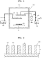
- FIG. 1 schematically illustrates a plasma-enhanced chemical vapor deposition (PECVD) apparatus 100 according to an exemplary embodiment.
- PECVD plasma-enhanced chemical vapor deposition
- the PECVD apparatus 100 includes a lithium (Li)-based film such as a LiPON film or a LiSiPON film that is deposited on a surface of a substrate 150.
- a lithium (Li)-based film such as a LiPON film or a LiSiPON film that is deposited on a surface of a substrate 150.
- the PECVD apparatus 100 may include a reaction chamber 110, first and second source supply units 120 and 130, a power supply unit 140, and a controller 180.
- a substrate 150 on which a Li-based film is to be deposited is placed in the reaction chamber 110.
- the substrate 150 may be loaded on a stage S.
- a reaction temperature of the substrate 150 may be, for example, about 100 °C to about 450 °C.
- the present exemplary embodiment is not limited thereto.
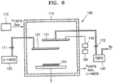
- FIG. 2 illustrates the substrate 150 on which a Li-based film is to be deposited.
- the substrate 150 may include at least one 3D structure 151 having a certain aspect ratio.
- Each 3D structure 151 may have an aspect ratio of, for example, 1:1 or greater, but the present exemplary embodiment is not limited thereto.
- the first source supply unit 120 may be provided outside the reaction chamber 110 to supply a Li source material into the reaction chamber 110.
- the Li source material may include at least one of, for example, lithium hexamethyldisilazide (Li-HMDS), Li(CH 2 SiMe 3 ), LiOtBu, Li(acac), and Li(thd).
- Li-HMDS lithium hexamethyldisilazide
- Li(CH 2 SiMe 3 ) LiOtBu
- Li(acac) Li(acac)
- Li(thd) Li(thd).
- the present exemplary embodiment is not limited thereto.
- a first source distribution unit 121 may be provided in the reaction chamber 110 and connected to the first source supply unit 120.
- the first source distribution unit 121 may uniformly distribute in the reaction chamber 110 the Li source material supplied by the first source supply unit 120.
- a first valve 171 may be disposed at a conduit that connects the first source supply unit 120 to the first source distribution unit 121 to control the passage of the Li source material through the conduit.
- the first valve 71 may be provided between the first source supply unit 120 and the first source distribution unit 121 to regulate the flow of the Li source material that moves into the reaction chamber 110.
- a Si source material may be further supplied into the reaction chamber 110 in addition to the Li source material,.
- the Li source material may be adsorbed on a surface of the substrate 150.
- the second source supply unit 130 may be provided outside the reaction chamber 110 and supply phosphor (P) and oxygen (O) source materials and a nitrogen (N) source material into the reaction chamber 110.
- the P and O source materials may include at least one of trimethyl phosphate (TMPO), triethyl phosphate (TEPO), and diethyl phosphoramidate (DEPA).
- TMPO trimethyl phosphate
- TEPO triethyl phosphate
- DEPA diethyl phosphoramidate
- the present exemplary embodiment is not limited thereto and the N source material may include at least one of a N 2 reactive gas and NH 3 reactive gas.
- the N source material may be used as a reactive gas and may also move the P and O source materials into the reaction chamber 110. In FIG. 1 , for example, a N 2 reactive gas is used as the N source material.
- a second source distribution unit 131 may be provided in the reaction chamber 110 and connected to the second source supply unit 130.
- the second source distribution unit 131 may uniformly distribute in the reaction chamber 110 the P and O source materials and the N source material supplied by the second source supply unit 130.
- a second valve 172 may be disposed at a conduit that connects the second source supply unit 130 to the second source distribution unit 131 to control the passage of the P and O source materials and the N source material through the conduit.
- the second valve 172 may be provided between the second source supply unit 130 and the second source distribution unit 131 to regulate the flow of the P and O source materials and the N source material into the reaction chamber 110.
- the second source supply unit 130 may supply the source materials into the reaction chamber 110 with a time gap from a supply time of the first source supply unit 120.
- the first source supply unit 120 first supplies the Li source material into the reaction chamber 110.
- the Li source material is adsorbed on the surface of the substrate 150.
- impurities including the Li source material remaining in the reaction chamber 110 are removed by purging.
- the second source supply unit 130 supplies the P and O source materials and the N source material into the reaction chamber 110.
- the P and O source materials and the N source material are supplied into the reaction chamber 110 from the second source supply unit 130 via the second source distribution unit 131, the P and O source materials may be adsorbed on Li source material on the surface of the substrate 150.
- the power supply unit 140 may supply power to generate plasma in the reaction chamber 110.
- the power supply unit 140 may include, for example, radio frequency (RF) power, the present exemplary embodiment is not limited thereto.
- RF radio frequency
- the controller 180 may turn on or off the plasma generated in the reaction chamber 110 by controlling the power supply unit 140.
- the controller 180 may be implemented by a processor and integrated into the power supply unit 140.
- the controller 180 may generate plasma in the reaction chamber 110 by driving the power supply unit 140 in the process in which the second source supply unit 130 supplies the P and O source materials and the N source material into the reaction chamber 110.
- the controller 180 may generate plasma in the reaction chamber 110 in the second period of the process in which the second source supply unit 130 supplies the P and O source materials and the N source material into the reaction chamber 110.
- the P and O source materials may be adsorbed on the Li source material on the surface of the substrate 150.
- plasma is generated in the reaction chamber 110.
- P-N bonding is formed and, the source materials adsorbed on the surface of the substrate 150 react to each other, and thus a Li-based film may be deposited on the surface of the substrate 150.
- the controller 180 may generate plasma in the reaction chamber 110 by driving the power supply unit 140 in the process in which the second source supply unit 130 supplies the P and O source materials and the N source material into the reaction chamber 110.
- the controller 180 controls an on-off time of plasma, an amount of the N source material such as a N 2 gas supplied into the reaction chamber 110 may be regulated.
- the Li-based film may be deposited at a relatively fast speed and uniformly on a surface of the 3D structure having a high aspect ratio, as described below, by using the PECVD apparatus 100 according to the embodiment.
- a method of forming a Li-based film on a surface of a substrate according to an exemplary embodiment is described hereinafter.
- the same process is repeated a plurality of times in a process of forming a Li-based film.
- one cycle of the process is described for convenience of explanation.
- FIG. 3 is a process diagram schematically illustrating a method of forming a Li-based film according to an embodiment.
- FIG. 4 is a flowchart of the method of FIG. 3 .
- a Li source material is supplied into the reaction chamber 110 of FIG. 1 in which the substrate 150 of FIG. 1 is placed (operation S210).
- a reaction temperature of the substrate 150 may be, for example, about 100 °C to about 450 °C, the present exemplary embodiment is not limited thereto.
- the process of supplying the Li source material may be performed from a start point to a point t1 in the process diagram of FIG. 3 . As such, when the Li source material is supplied into the reaction chamber 110, the Li source material may be adsorbed on the surface of the substrate 150.
- the interior of the reaction chamber 110 is first purged (operation S220).
- the first purging may be performed from the point t1 to a point t2 in the process diagram of FIG. 3 . Accordingly, impurities including the Li source material remaining in the reaction chamber 110 may be removed by the first purging.
- the P and O source materials and the N source material are supplied into the reaction chamber 110 (operation S230).
- the process of supplying the P and O source materials and the N source material may be performed from the point t2 to a point t4 in the process diagram of FIG. 3 .
- Plasma is generated in the reaction chamber 110 in the process of supplying the P and O source materials and the N source material into the reaction chamber 110 the reaction chamber 110 (operation S240).
- plasma is generated in the reaction chamber 110 in the second period of the process of supplying the P and O source materials and the N source material into the reaction chamber 110.
- the process of generating plasma in the reaction chamber 110 may be performed from a point t3 to the point t4 in the process diagram of FIG. 3 .
- the reaction chamber 110 In the first period of the process of supplying the P and O source materials and the N source material into the reaction chamber 110, that is, in the state in which no plasma is generated in a period from the point t2 to the point t3 in the process diagram of FIG. 3 , the reaction chamber 110, the P and O source materials and the N source material are supplied into the reaction chamber 110. Accordingly, the interior of the reaction chamber 110 is in an atmosphere of the N source material, and the P and O source materials may be adsorbed on the Li source material on the surface of the substrate 150.
- plasma is generated as the P and O source materials and the N source material are supplied into the reaction chamber 110.
- the P-N bonding is formed and the source materials on the surface of the substrate 150 react to each other and thus a Li-based film may be deposited.
- an amount of the N source material supplied into the reaction chamber 110 may be regulated by controlling the on-off time of plasma.
- the interior of the reaction chamber 110 is second purged (operation S250).
- the second purging may be performed from the point t4 to a point t5 in the process diagram of FIG. 3 .
- Impurities including the P and O source materials remaining in the reaction chamber 110 may be removed by the second purging.
- FIGS. 5A, 5B , 6 , 7A, 7B , 8A, 8B , and 9 illustrate in detail a process of forming a Li-based film on a surface of the substrate 150 by using the PECVD apparatus 100 of FIG. 1 .
- FIG. 5A illustrates that the Li source material is supplied into the reaction chamber 110.
- FIG. 5B illustrates that the Li source material is adsorbed on the surface of the substrate 150.
- the substrate 150 on which a Li-based film is to be deposited is prepared in the reaction chamber 110.
- the substrate 150 may include at least one 3D structure 151 having an aspect ratio of, for example, 1:1 or greater, but the present exemplary embodiment is not limited thereto.
- a reaction temperature of the substrate 150 may be, for example, about 100 °C to about 450 °C, but the present exemplary embodiment is not limited thereto.
- the first source supply unit 120 supplies the Li source material into the reaction chamber 110.
- no plasma is generated in the reaction chamber 110.
- the processing supplying the Li source material may be performed from the start point to the point t1 in the process diagram of FIG. 3 .
- the Li source material supplied into the reaction chamber 110 may include at least one of, for example, Li-HMDS, Li(CH 2 SiMe 3 ), LiOtBu, Li(acac), and Li(thd), but the present exemplary embodiment is not limited thereto.
- FIG. 5A illustrates an example of using Li-HMDS as the Li source material.
- the first source supply unit 120 may uniformly supply the Li source material, for example, Li-HMDS, into the reaction chamber 110 through the first source distribution unit 121.
- the Li source material for example, Li-HMDS
- the Li source material may be adsorbed on the surface of the substrate 150 including the 3D structure 151, as illustrated in FIG. 5B .
- FIG. 6 illustrates that the interior of the reaction chamber 110 is first purged.
- the PECVD apparatus 100 may further include a purging gas supply unit 173.
- the purging gas may be, for example, an inert gas such as a N 2 gas.
- the purging gas such as a N 2 gas
- the impurities including the Li source material remaining in the reaction chamber 110 are discharged to the outside of the reaction chamber 110 with the N 2 gas by the purging. Accordingly, the impurities remaining in the reaction chamber 110 may be removed.
- the first purging may be performed from the point t1 to the point t2 in the process diagram of FIG. 3 .
- FIG. 7A illustrates that the P and O source materials and the N source material are supplied into the reaction chamber 110.
- FIG. 7B illustrates that the P and O source materials are adsorbed on the surface of the substrate 150.
- the second source supply unit 130 supplies the P and O source materials and the N source material into the reaction chamber 110.
- no plasma is generated in the reaction chamber 110.
- the process of supplying the P and O source materials and the N source material into the reaction chamber 110 in a state in which no plasma is generated in the reaction chamber 110 may be performed from the point t2 to the point t3 in the process diagram of FIG. 3 .
- FIG. 7A illustrates an example of using TMPO as the P and O source materials.
- the N source material may include at least one of a N 2 reactive gas and a NH 3 reactive gas.
- the N source material may be used as the reactive gas and also move the P and O source materials to the reaction chamber 110.
- FIG. 7A illustrates an example of using a N 2 reactive gas as the N source material.
- the second source supply unit 130 may uniformly supply the P and O source materials, for example, TMPO, and the N source material, for example, the N 2 reactive gas, into the reaction chamber 110 through the second source distribution unit 131.
- the P and O source materials, for example, TMPO, and the N source material, for example, the N 2 reactive gas are supplied into the reaction chamber 110 in a state in which no plasma is generated in the reaction chamber 110, a nitrogen atmosphere is formed in the reaction chamber 110 and, as illustrated in FIG. 7B , the P and O source materials, for example, TMPO, may be adsorbed on the Li source material, for example, Li-HMDS, of the substrate 150.
- FIG. 8A illustrates that plasma is generated in the reaction chamber 110 during a process of supplying the P and O source materials and the N source material into the reaction chamber 110.
- FIG. 8B illustrates that a Li-based film 190 is deposited on the surface of the substrate 150.
- plasma is generated in the reaction chamber 110.
- the plasma is generated by driving of the power supply unit 140.
- a plasma generation time may be adjusted.
- the process of generating plasma in the reaction chamber 110 during the process of supplying the P and O source materials and the N source material into the reaction chamber 110 may be performed from the point t3 to the point t4 in the process diagram of FIG. 3 .
- the process of supplying the P and O source materials and the N source material into the reaction chamber 110 may be performed from the point t2 to the point t4 in the process diagram of FIG. 3 .
- the P and O source materials and the N source material may be supplied into the reaction chamber 110 in a state in which no plasma is generated in the reaction chamber 110.
- the second period of the process of supplying the P and O source materials and the N source material that is, in a period from the point t3 to the point t4 in the process diagram of FIG.
- the P and O source materials and the N source material may be supplied into the reaction chamber 110 in a state in which plasma is generated in the reaction chamber 110.
- the amount of the N source material supplied into the reaction chamber 110 may be adjusted by controlling the on-off time of plasma generated in the reaction chamber 110 by using the controller 180.
- the Li-based film 190 may be formed on the surface of the substrate 150.
- the Li-based film 190 may include, for example, a LiPON film or a LiSiPON film, but the present exemplary embodiment is not limited thereto.
- FIG. 9 illustrates that the interior of the reaction chamber 110 is second purged.
- the impurities including the P and O source materials and so forth remaining in the reaction chamber 110 are removed by using the purging gas supplied from the purging gas supply unit 173.
- the purging gas may be, for example, an inert gas such as a N 2 gas.
- the purging gas such as a N 2 gas
- the impurities including the P and O source materials and so forth remaining in the reaction chamber 110 are discharged to the outside of the reaction chamber 110 with the N 2 gas by the purging. Accordingly, the impurities including the P and O source materials and so forth remaining in the reaction chamber 110 may be removed.
- the second purging may be performing from the point t4 to the point t5 in the process diagram of FIG. 3 .
- the Li-based film 190 having a desired thickness may be formed by repeating the one cycle process.
- the process of supplying the Li source material into the reaction chamber 110 and the process of supplying the P and O source materials and the N source material into the reaction chamber 110 are performed with a time interval. Accordingly, when plasma is generated in the reaction chamber 110 in the process of supplying the P and O source materials and the N source material into the reaction chamber 110, the impurities including the Li source material are prevented from intruding into the reaction chamber 110. Also, as the controller 180 controls the on-off time of plasma, the supply of the N source material into the reaction chamber 110 may be easily controlled.
- the source materials are adsorbed on the surface of the substrate 150 in a state in which plasma is not generated, a step coverage problem may be solved. Also, since the Li-based film 190 is deposited in a state in which plasma is generated, the Li-based film 190 may be formed at a relatively fast speed. Accordingly, the Li-based film 190 may be uniformly and at a relatively fast speed deposited on a 3D structure having a high aspect ratio.
- a technology of depositing inorganic-based solid electrolyte film such as LiPON on cathodes using a chemical vapor deposition (CVD) method to implement a high output micro battery cell has been reported.
- CVD chemical vapor deposition
- the cathodes may be damaged.
- a technology of depositing a solid electrolyte film on an electrode having a 3D structure by the PECVD using nitrogen plasma has been reported.
- a step coverage is generated when an electrode has a 3D structure having a high aspect ratio.
- the process of supplying the Li source material and the process of supplying the P and O source materials and the N source material are separated in terms of time, and the source materials are adsorbed on the surface of the substrate 150 in a state in which no plasma is generated, thereby solving the step coverage problem. Also, since the Li-based film 190 is deposited in a state in which plasma is generated in the process of supplying the P and O source materials and the N source material, the Li-based film 190 may be formed at a relatively fast speed.
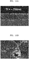
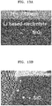
- FIG. 10 is an image of the Li-based film formed on 3D structures by sputtering.
- FIGS. 11A, 11B , 11C, 11D , 11E, and 11F are magnified images of respective portions A, B, C, D, E, and F of FIG. 10 .
- silicon having a surface on which a silicon oxide film is formed is used as the 3D structures, and a LiPON film is used as the Li-based electrolyte film.
- the width and height of each of the 3D structures are about 10 ⁇ m and about 100 ⁇ m, respectively, and an interval between the 3D structures is about 10 ⁇ m.
- a Li-based electrolyte film is irregularly formed on surfaces of the 3D structures.
- a thickness Tt of the Li-based electrolyte film (LiPON film) formed on top of the 3D structure is about 700 nm
- a thickness Ts of the Li-based electrolyte film (LiPON film) formed on a bottom of the 3D structure may be about 0 nm. Accordingly, when the Li-based electrolyte film is deposited on the 3D structure having a high aspect ratio by sputtering, a step coverage problem may be generated.
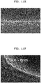
- FIG. 12 is an image of a Li-based electrolyte film formed on 3D structures by a PECVD method, according to an exemplary embodiment.
- FIGS. 13A, 13B , 13C, 13D , 13E, and 13F are magnified images of respective portions A, B, C, D, E, and F of FIG. 12 .
- silicon having a surface on which a silicon oxide film is formed is used as the 3D structures, and a LiPON film is used as the Li-based electrolyte film.
- the width and height of each of the 3D structures are about 10 ⁇ m and about 100 ⁇ m, respectively, and an interval between the 3D structures is about 10 ⁇ m.
- a Li-based electrolyte film is relatively uniformly formed on surfaces of the 3D structures.
- a thickness Tt of the Li-based electrolyte film formed on top of the 3D structure is about 430 nm
- a thickness Ts of the Li-based electrolyte film formed on a bottom of the 3D structure may be about 150 nm. Accordingly, when the Li-based film is deposited on the 3D structure having a high aspect ratio by the PECVD method according to the present embodiment, the step coverage problem may be solved.
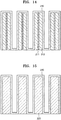
- FIG. 14 illustrates a Li-based film 290 formed on cathodes 212 having a 3D structure, according to another embodiment.
- the Li-based film 290 is deposited on a plurality of 3D structures arranged parallel to each other.
- Each of the 3D structures may include a collector 211 and a cathode 212 provided on both sides of the collector 211.
- Each of the 3D structures may have a high aspect ratio of, for example, 1:1 or greater.
- the Li-based film 290 deposited on the 3D structures may be a solid electrolyte film.
- the Li-based film 290 may be formed by the PECVD method according to the above-described embodiment.
- FIG. 15 illustrates a Li-based film 390 formed on anodes 320 having a 3D structure, according to another exemplary embodiment.
- the Li-based film 390 is deposited on the anodes 320 having a 3D structure arranged parallel to each other.
- Each of the anodes 320 may have a high aspect ratio of, for example 1:1 or greater.
- the Li-based film 390 deposited on the anodes 320 having a 3D structure may be a solid electrolyte film or a protective film.
- the Li-based film 390 may be formed by the PECVD method according to the above-described exemplary embodiment.
- FIG. 16 illustrates a Li-based film 490 formed on conductive carbon electrodes 420 having a 3D structure, according to another exemplary embodiment.
- the Li-based film 490 is deposited on the conductive carbon electrodes 420 having a 3D structure arranged parallel to each other.
- the conductive carbon electrodes 420 are electrodes used for metal-air batteries and may have a high aspect ratio of, for example, 1:1 or greater.
- the Li-based film 490 deposited on the conductive carbon electrodes 420 having a 3D structure may be a solid electrolyte film or a protective film.
- the Li-based film 490 may be formed by the PECVD method according to the above-described exemplary embodiment.
- the process of supplying the Li source material into the reaction chamber to form a Li-based film and the process of supplying the P and O source materials and the N source material into the reaction chamber are performed with a time interval. Accordingly, when plasma is generated in the process of supplying the P and O source materials and the N source material into the reaction chamber, the intrusion of the Li source material and so forth and the impurities into the reaction chamber may be prevented. Also, as the controller controls the on-off time of plasma, the supply of the N source material into the reaction chamber may be easily controlled.
- the step coverage problem may be solved. Since the Li-based film is deposited in a state in which plasma is generated in the reaction chamber, the Li-based film may be formed at a relatively fast speed. Accordingly, the Li-based film may be uniformly deposited on the 3D structure having a high aspect ratio at a relatively fast speed.
- the Li-based film may be deposited on the electrode having, for example, a 3D structure to be used as a solid electrolyte film or a protective film. Also, the Li-based film may be deposited on a conductive carbon electrode of a metal-air battery to be used as a solid electrolyte film or a protective film.
- the present exemplary embodiment is not limited thereto and may be applied to other various fields.
Landscapes
- Chemical & Material Sciences (AREA)
- Engineering & Computer Science (AREA)
- General Chemical & Material Sciences (AREA)
- Chemical Kinetics & Catalysis (AREA)
- Materials Engineering (AREA)
- Mechanical Engineering (AREA)
- Metallurgy (AREA)
- Organic Chemistry (AREA)
- Physics & Mathematics (AREA)
- Plasma & Fusion (AREA)
- Electrochemistry (AREA)
- Manufacturing & Machinery (AREA)
- Inorganic Chemistry (AREA)
- Analytical Chemistry (AREA)
- Condensed Matter Physics & Semiconductors (AREA)
- General Physics & Mathematics (AREA)
- Chemical Vapour Deposition (AREA)
- Battery Electrode And Active Subsutance (AREA)
- Formation Of Insulating Films (AREA)
Description
- Apparatuses and methods consistent with exemplary embodiments relate to forming a lithium (Li)-based film.
- Due to the development of technologies in the field of electronics, the market for portable electronic devices (e.g., smartphones, smartpads, e-book readers, tablet computers, etc.) has rapidly grown. As the market grows, the demand for batteries suitable for operating such portable electronic devices has increased as well.
- Unlike primary batteries that are not chargeable, secondary batteries refer to batteries that are chargeable and dischargeable. In particular, lithium secondary batteries have an advantage of a high energy density per unit weight. High power secondary batteries using an electrode having a three-dimensional (3D) structure has been developed. In this regard, the technologies to form a Li-based solid electrolyte film on a 3D-structured electrode have been developed.
-
US2005/0008772 teaches a method of producing LiPON using a plasma deposition process. Kozen et a, "Atomic Layer Deposition of the Solid Electrolye LiPON", Chemistry of Materials (2015) volume 27 pages 5324 to 5331 teaches a sequential atomic layer deposition (ALD) process for depositing LiPON. - One or more exemplary embodiments provide a plasma-enhanced chemical vapor deposition apparatus and a method of forming a lithium (Li)-based film by using the same
- According to an aspect of an embodiment, there is provided a plasma-enhanced chemical vapor deposition apparatus according to claim 9.
- The Li source material supplied into the reaction chamber by the first source supply may be adsorbed on the surface of the substrate, and the P and O source materials supplied into the reaction chamber by the second source supply is adsorbed on the Li source material.
- When the second source supply supplies the P and O source materials and the N source material into the reaction chamber, the controller may control the power supply to form a bonding between the P source material and the N source material (P-N bonding) using the plasma.
- The controller may control an on-off time of the generation of the plasma to adjust an amount of the N source material supplied into the reaction chamber.
- The Li source material may include at least one of lithium hexamethyldisilazide (Li-HMDS), Li(CH2SiMe3), LiOtBu, Li(acac), and Li(thd). The P and O source materials may include at least one of trimethyl phosphate (TMPO), triethyl phosphate (TEPO), and diethyl phosphoramidate (DEPA).
- The N source material may include at least one of a N2 reactive gas and a NH3 reactive gas that move the P and O source materials into the reaction chamber.
- According to an aspect of the invention there is provided a method of forming a lithium (Li)-based film according to
claim 1. - The method may further include purging an interior of the reaction chamber between the supplying of the Li source material into the reaction chamber and the supplying of the P and O source materials and the N source material into the reaction chamber.
- The Li source material supplied into the reaction chamber may be deposited on the substrate, and the P and O source materials supplied into the reaction chamber may be adsorbed on the Li source material.
- A bonding between the P source material and the N source material (P-N bonding) may be formed by generating the plasma in the reaction chamber when the P and O source materials and the N source material are supplied into the reaction chamber.
- An amount of the N source material supplied into the reaction chamber may be adjusted by controlling an on-off time of generation of the plasma. The method may further include purging an interior of the reaction chamber after the Li-based film is formed on the substrate. A reaction temperature of the substrate in a process of forming the Li-based film may be about 100 °C to about 450 °C.
- The substrate may include at least one three-dimensional (3D) structure having an aspect ratio of 1:1 or greater. The 3D structure may include a cathode having a 3D structure, and the Li-based film may include a solid electrolyte film deposited on a surface of the cathode.
- The 3D structure may include an anode having a 3D structure, and the Li-based film may include a solid electrolyte film or a protective film deposited on a surface of the anode. The 3D structure may include a conductive carbon electrode having a 3D structure, and the Li-based film may include a solid electrolyte film or a protective film deposited on a surface of the conductive carbon electrode.
- According to an exemplary embodiment, there is provided a plasma-enhanced chemical vapor deposition apparatus including: a substrate disposed in a reaction chamber; a first source supply configured to supply a Li source material into the reaction chamber at a first time to deposit the first time to deposit the Li source material on the substrate; a second source supply configured to supply phosphor (P) and oxygen (O) source materials and a nitrogen (N) source material into the reaction chamber at a second time subsequent to the first time to be adsorbed by the Li source material deposited on the substrate; and a power supply configured to supply power into the reaction chamber to generate plasma that causes the P source material to react with the N source material at the second time.
- The apparatus may further include a purging gas supply configured to supply a purging gas into the reaction chamber to remove the Li source material remaining in the chamber after the Li source material is deposited on the substrate at time t1 before the P, O, and N source materials are supplied into the reaction chamber at the second time,
- The power supply may be further configured to control an on-off time of generation of the plasma at the second time.
- The above and/or other aspects will be more apparent by describing certain exemplary embodiments, with reference to the accompanying drawings, in which:
-
FIG. 1 schematically illustrates a plasma-enhanced chemical vapor deposition apparatus according to an exemplary embodiment; -
FIG. 2 is an enlarged view of a substrate ofFIG. 1 ; -
FIG. 3 is a process diagram schematically illustrating a method of forming a lithium (Li)-based film, according to an exemplary embodiment; -
FIG. 4 is a flowchart of the method ofFIG. 3 ; -
FIGS. 5A, 5B ,6 ,7A, 7B ,8A, 8B , and9 illustrate a process of forming a Li-based film on a surface of the substrate by using the plasma-enhanced chemical vapor deposition apparatus ofFIG. 1 ; -
FIG. 10 is an image of the Li-based film formed on three-dimensional (3D) structures by sputtering; -
FIGS. 11A, 11B ,11C, 11D ,11E, and 11F are respective images of portions A, B, C, D, E, and F ofFIG. 10 ; -
FIG. 12 is an image of a Li-based film formed on 3D structures by a plasma-enhanced chemical vapor deposition method, according to an exemplary embodiment; -
FIGS. 13A, 13B ,13C, 13D ,13E, and 13F are respective images of portions A, B, C, D, E, and F ofFIG. 12 ; -
FIG. 14 illustrates a Li-based film formed on cathodes having a 3D structure, according to another exemplary embodiment; -
FIG. 15 illustrates a Li-based film formed on anodes having a 3D structure, according to another exemplary embodiment; and -
FIG. 16 illustrates a Li-based film formed on conductive carbon electrodes having a 3D structure, according to another exemplary embodiment. - Exemplary embodiments are described in greater detail below with reference to the accompanying drawings.
- In the following description, like drawing reference numerals are used for like elements, even in different drawings. The matters defined in the description, such as detailed construction and elements, are provided to assist in a comprehensive understanding of the exemplary embodiments. However, it is apparent that the exemplary embodiments can be practiced without those specifically defined matters. Also, well-known functions or constructions are not described in detail since they would obscure the description with unnecessary detail.
-
FIG. 1 schematically illustrates a plasma-enhanced chemical vapor deposition (PECVD)apparatus 100 according to an exemplary embodiment. - Referring to
FIG. 1 , thePECVD apparatus 100 according to the exemplary embodiment includes a lithium (Li)-based film such as a LiPON film or a LiSiPON film that is deposited on a surface of asubstrate 150. - The
PECVD apparatus 100 may include areaction chamber 110, first and secondsource supply units power supply unit 140, and acontroller 180. Asubstrate 150 on which a Li-based film is to be deposited is placed in thereaction chamber 110. Thesubstrate 150 may be loaded on a stage S. In a film forming process, a reaction temperature of thesubstrate 150 may be, for example, about 100 °C to about 450 °C. However, the present exemplary embodiment is not limited thereto. -
FIG. 2 illustrates thesubstrate 150 on which a Li-based film is to be deposited. Referring toFIG. 2 , thesubstrate 150 may include at least one3D structure 151 having a certain aspect ratio. The aspect ratio denotes a ratio of a height h to a width d of the 3D structure 151 (e.g. the ratio of h to d = h:d = h/d). Each3D structure 151 may have an aspect ratio of, for example, 1:1 or greater, but the present exemplary embodiment is not limited thereto. - The first
source supply unit 120 may be provided outside thereaction chamber 110 to supply a Li source material into thereaction chamber 110. The Li source material may include at least one of, for example, lithium hexamethyldisilazide (Li-HMDS), Li(CH2SiMe3), LiOtBu, Li(acac), and Li(thd). However, the present exemplary embodiment is not limited thereto. - A first
source distribution unit 121 may be provided in thereaction chamber 110 and connected to the firstsource supply unit 120. The firstsource distribution unit 121 may uniformly distribute in thereaction chamber 110 the Li source material supplied by the firstsource supply unit 120. Afirst valve 171 may be disposed at a conduit that connects the firstsource supply unit 120 to the firstsource distribution unit 121 to control the passage of the Li source material through the conduit. The first valve 71 may be provided between the firstsource supply unit 120 and the firstsource distribution unit 121 to regulate the flow of the Li source material that moves into thereaction chamber 110. When the firstsource supply unit 120 uses a material including, for example, Li and Si, as a source material, a Si source material may be further supplied into thereaction chamber 110 in addition to the Li source material,. - In a state in which plasma is not yet generated in the
reaction chamber 110, when Li source material is supplied into thereaction chamber 110 from the firstsource supply unit 120 via the firstsource distribution unit 121, the Li source material may be adsorbed on a surface of thesubstrate 150. - The second
source supply unit 130 may be provided outside thereaction chamber 110 and supply phosphor (P) and oxygen (O) source materials and a nitrogen (N) source material into thereaction chamber 110. The P and O source materials may include at least one of trimethyl phosphate (TMPO), triethyl phosphate (TEPO), and diethyl phosphoramidate (DEPA). However, the present exemplary embodiment is not limited thereto and the N source material may include at least one of a N2 reactive gas and NH3 reactive gas. The N source material may be used as a reactive gas and may also move the P and O source materials into thereaction chamber 110. InFIG. 1 , for example, a N2 reactive gas is used as the N source material. - A second
source distribution unit 131 may be provided in thereaction chamber 110 and connected to the secondsource supply unit 130. The secondsource distribution unit 131 may uniformly distribute in thereaction chamber 110 the P and O source materials and the N source material supplied by the secondsource supply unit 130. Asecond valve 172 may be disposed at a conduit that connects the secondsource supply unit 130 to the secondsource distribution unit 131 to control the passage of the P and O source materials and the N source material through the conduit. Thesecond valve 172 may be provided between the secondsource supply unit 130 and the secondsource distribution unit 131 to regulate the flow of the P and O source materials and the N source material into thereaction chamber 110. - The second
source supply unit 130 may supply the source materials into thereaction chamber 110 with a time gap from a supply time of the firstsource supply unit 120. In detail, the firstsource supply unit 120 first supplies the Li source material into thereaction chamber 110. The Li source material is adsorbed on the surface of thesubstrate 150. Next, impurities including the Li source material remaining in thereaction chamber 110 are removed by purging. Then, the secondsource supply unit 130 supplies the P and O source materials and the N source material into thereaction chamber 110. - In a state in which plasma is not yet generated in the
reaction chamber 110, when the P and O source materials and the N source material are supplied into thereaction chamber 110 from the secondsource supply unit 130 via the secondsource distribution unit 131, the P and O source materials may be adsorbed on Li source material on the surface of thesubstrate 150. - The
power supply unit 140 may supply power to generate plasma in thereaction chamber 110. Although thepower supply unit 140 may include, for example, radio frequency (RF) power, the present exemplary embodiment is not limited thereto. Although thepower supply unit 140 may be connected to the secondsource distribution unit 131, the present exemplary embodiment is not limited thereto. Thecontroller 180 may turn on or off the plasma generated in thereaction chamber 110 by controlling thepower supply unit 140. Thecontroller 180 may be implemented by a processor and integrated into thepower supply unit 140. - The
controller 180 may generate plasma in thereaction chamber 110 by driving thepower supply unit 140 in the process in which the secondsource supply unit 130 supplies the P and O source materials and the N source material into thereaction chamber 110. In detail, thecontroller 180 may generate plasma in thereaction chamber 110 in the second period of the process in which the secondsource supply unit 130 supplies the P and O source materials and the N source material into thereaction chamber 110. - In detail, no plasma is generated in the
reaction chamber 110 in the first period of the process in which the secondsource supply unit 130 supplies the P and O source materials and the N source material into thereaction chamber 110. In this case, as described above, the P and O source materials may be adsorbed on the Li source material on the surface of thesubstrate 150. - In the second period of the process in which the second
source supply unit 130 supplies the P and O source materials and the N source material into thereaction chamber 110, as thecontroller 180 drives thepower supply unit 140, plasma is generated in thereaction chamber 110. In this case, as plasma is generated in thereaction chamber 110 in a nitrogen atmosphere, P-N bonding is formed and, the source materials adsorbed on the surface of thesubstrate 150 react to each other, and thus a Li-based film may be deposited on the surface of thesubstrate 150. - As such, the
controller 180 may generate plasma in thereaction chamber 110 by driving thepower supply unit 140 in the process in which the secondsource supply unit 130 supplies the P and O source materials and the N source material into thereaction chamber 110. In this case, when thecontroller 180 controls an on-off time of plasma, an amount of the N source material such as a N2 gas supplied into thereaction chamber 110 may be regulated. - The Li-based film may be deposited at a relatively fast speed and uniformly on a surface of the 3D structure having a high aspect ratio, as described below, by using the
PECVD apparatus 100 according to the embodiment. - A method of forming a Li-based film on a surface of a substrate according to an exemplary embodiment is described hereinafter. In general, the same process is repeated a plurality of times in a process of forming a Li-based film. In the following description, one cycle of the process is described for convenience of explanation.
-
FIG. 3 is a process diagram schematically illustrating a method of forming a Li-based film according to an embodiment.FIG. 4 is a flowchart of the method ofFIG. 3 . - Referring to
FIGS. 3 and 4 , a Li source material is supplied into thereaction chamber 110 ofFIG. 1 in which thesubstrate 150 ofFIG. 1 is placed (operation S210). In this state, although a reaction temperature of thesubstrate 150 may be, for example, about 100 °C to about 450 °C, the present exemplary embodiment is not limited thereto. The process of supplying the Li source material may be performed from a start point to a point t1 in the process diagram ofFIG. 3 . As such, when the Li source material is supplied into thereaction chamber 110, the Li source material may be adsorbed on the surface of thesubstrate 150. - Next, the interior of the
reaction chamber 110 is first purged (operation S220). The first purging may be performed from the point t1 to a point t2 in the process diagram ofFIG. 3 . Accordingly, impurities including the Li source material remaining in thereaction chamber 110 may be removed by the first purging. - Next, the P and O source materials and the N source material are supplied into the reaction chamber 110 (operation S230). The process of supplying the P and O source materials and the N source material may be performed from the point t2 to a point t4 in the process diagram of
FIG. 3 . Plasma is generated in thereaction chamber 110 in the process of supplying the P and O source materials and the N source material into thereaction chamber 110 the reaction chamber 110 (operation S240). In detail, plasma is generated in thereaction chamber 110 in the second period of the process of supplying the P and O source materials and the N source material into thereaction chamber 110. The process of generating plasma in thereaction chamber 110 may be performed from a point t3 to the point t4 in the process diagram ofFIG. 3 . - In the first period of the process of supplying the P and O source materials and the N source material into the
reaction chamber 110, that is, in the state in which no plasma is generated in a period from the point t2 to the point t3 in the process diagram ofFIG. 3 , thereaction chamber 110, the P and O source materials and the N source material are supplied into thereaction chamber 110. Accordingly, the interior of thereaction chamber 110 is in an atmosphere of the N source material, and the P and O source materials may be adsorbed on the Li source material on the surface of thesubstrate 150. - In the second period of the process of supplying the P and O source materials and the N source material into the
reaction chamber 110, that is, in a period from the point t3 to the point t4 in the process diagram ofFIG. 3 , plasma is generated as the P and O source materials and the N source material are supplied into thereaction chamber 110. As such, when plasma is generated in thereaction chamber 110, the P-N bonding is formed and the source materials on the surface of thesubstrate 150 react to each other and thus a Li-based film may be deposited. In this state, an amount of the N source material supplied into thereaction chamber 110 may be regulated by controlling the on-off time of plasma. - Finally, the interior of the
reaction chamber 110 is second purged (operation S250). The second purging may be performed from the point t4 to a point t5 in the process diagram ofFIG. 3 . Impurities including the P and O source materials remaining in thereaction chamber 110 may be removed by the second purging. -
FIGS. 5A, 5B ,6 ,7A, 7B ,8A, 8B , and9 illustrate in detail a process of forming a Li-based film on a surface of thesubstrate 150 by using thePECVD apparatus 100 ofFIG. 1 . -
FIG. 5A illustrates that the Li source material is supplied into thereaction chamber 110.FIG. 5B illustrates that the Li source material is adsorbed on the surface of thesubstrate 150. - Referring to
FIG. 5A , thesubstrate 150 on which a Li-based film is to be deposited is prepared in thereaction chamber 110. Thesubstrate 150 may include at least one3D structure 151 having an aspect ratio of, for example, 1:1 or greater, but the present exemplary embodiment is not limited thereto. In the process of forming a Li-based film, a reaction temperature of thesubstrate 150 may be, for example, about 100 °C to about 450 °C, but the present exemplary embodiment is not limited thereto. - Next, the first
source supply unit 120 supplies the Li source material into thereaction chamber 110. In the process, no plasma is generated in thereaction chamber 110. The processing supplying the Li source material may be performed from the start point to the point t1 in the process diagram ofFIG. 3 . - The Li source material supplied into the
reaction chamber 110 may include at least one of, for example, Li-HMDS, Li(CH2SiMe3), LiOtBu, Li(acac), and Li(thd), but the present exemplary embodiment is not limited thereto.FIG. 5A illustrates an example of using Li-HMDS as the Li source material. - The first
source supply unit 120 may uniformly supply the Li source material, for example, Li-HMDS, into thereaction chamber 110 through the firstsource distribution unit 121. As such, when the Li source material is supplied in a state in which no plasma is generated in thereaction chamber 110, the Li source material, for example, Li-HMDS, may be adsorbed on the surface of thesubstrate 150 including the3D structure 151, as illustrated inFIG. 5B . -
FIG. 6 illustrates that the interior of thereaction chamber 110 is first purged. ThePECVD apparatus 100 may further include a purginggas supply unit 173. - Referring to
FIG. 6 , as described above, after the Li source material is adsorbed on the surface of thesubstrate 150, impurities including the Li source material remaining in thereaction chamber 110 are removed by using a purging gas supplied from the purginggas supply unit 173. The purging gas may be, for example, an inert gas such as a N2 gas. In detail, when the purging gas such as a N2 gas is supplied into thereaction chamber 110, the impurities including the Li source material remaining in thereaction chamber 110 are discharged to the outside of thereaction chamber 110 with the N2 gas by the purging. Accordingly, the impurities remaining in thereaction chamber 110 may be removed. The first purging may be performed from the point t1 to the point t2 in the process diagram ofFIG. 3 . -
FIG. 7A illustrates that the P and O source materials and the N source material are supplied into thereaction chamber 110.FIG. 7B illustrates that the P and O source materials are adsorbed on the surface of thesubstrate 150. - Referring to
FIG. 7A , the secondsource supply unit 130 supplies the P and O source materials and the N source material into thereaction chamber 110. In this process, no plasma is generated in thereaction chamber 110. As such, the process of supplying the P and O source materials and the N source material into thereaction chamber 110 in a state in which no plasma is generated in thereaction chamber 110 may be performed from the point t2 to the point t3 in the process diagram ofFIG. 3 . - Although the P and O source materials supplied into the
reaction chamber 110 may include at least one of TMPO, TEPO, and DEPA, the present exemplary embodiment is not limited thereto.FIG. 7A illustrates an example of using TMPO as the P and O source materials. The N source material may include at least one of a N2 reactive gas and a NH3 reactive gas. The N source material may be used as the reactive gas and also move the P and O source materials to thereaction chamber 110.FIG. 7A illustrates an example of using a N2 reactive gas as the N source material. - The second
source supply unit 130 may uniformly supply the P and O source materials, for example, TMPO, and the N source material, for example, the N2 reactive gas, into thereaction chamber 110 through the secondsource distribution unit 131. As such, when the P and O source materials, for example, TMPO, and the N source material, for example, the N2 reactive gas, are supplied into thereaction chamber 110 in a state in which no plasma is generated in thereaction chamber 110, a nitrogen atmosphere is formed in thereaction chamber 110 and, as illustrated inFIG. 7B , the P and O source materials, for example, TMPO, may be adsorbed on the Li source material, for example, Li-HMDS, of thesubstrate 150. -
FIG. 8A illustrates that plasma is generated in thereaction chamber 110 during a process of supplying the P and O source materials and the N source material into thereaction chamber 110.FIG. 8B illustrates that a Li-basedfilm 190 is deposited on the surface of thesubstrate 150. - Referring to
FIG. 8A , in the process of supplying the P and O source materials and the N source material into thereaction chamber 110, plasma is generated in thereaction chamber 110. The plasma is generated by driving of thepower supply unit 140. As thecontroller 180 controls the driving of thepower supply unit 140, a plasma generation time may be adjusted. As such, the process of generating plasma in thereaction chamber 110 during the process of supplying the P and O source materials and the N source material into thereaction chamber 110 may be performed from the point t3 to the point t4 in the process diagram ofFIG. 3 . - The process of supplying the P and O source materials and the N source material into the
reaction chamber 110 may be performed from the point t2 to the point t4 in the process diagram ofFIG. 3 . In this regard, in the first period of the process of supplying the P and O source materials and the N source material, that is, in a period from the point t2 to the point t3 in the process diagram ofFIG. 3 , the P and O source materials and the N source material may be supplied into thereaction chamber 110 in a state in which no plasma is generated in thereaction chamber 110. In the second period of the process of supplying the P and O source materials and the N source material, that is, in a period from the point t3 to the point t4 in the process diagram ofFIG. 3 , the P and O source materials and the N source material may be supplied into thereaction chamber 110 in a state in which plasma is generated in thereaction chamber 110. The amount of the N source material supplied into thereaction chamber 110 may be adjusted by controlling the on-off time of plasma generated in thereaction chamber 110 by using thecontroller 180. - As illustrated in
FIG. 8A , when plasma is generated in thereaction chamber 110 during the process of supplying the P and O source materials and the N source material into thereaction chamber 110, the P-N bonding is formed in a nitrogen atmosphere and the source materials adsorbed on the surface of thesubstrate 150 react to each other. Accordingly, as illustrated inFIG. 8B , the Li-basedfilm 190 may be formed on the surface of thesubstrate 150. In this state, the Li-basedfilm 190 may include, for example, a LiPON film or a LiSiPON film, but the present exemplary embodiment is not limited thereto. -
FIG. 9 illustrates that the interior of thereaction chamber 110 is second purged. - Referring to
FIG. 9 , as described above, after the Li-basedfilm 190 is formed on the surface of thesubstrate 150, the impurities including the P and O source materials and so forth remaining in thereaction chamber 110 are removed by using the purging gas supplied from the purginggas supply unit 173. The purging gas may be, for example, an inert gas such as a N2 gas. In detail, when the purging gas such as a N2 gas is supplied into thereaction chamber 110, the impurities including the P and O source materials and so forth remaining in thereaction chamber 110 are discharged to the outside of thereaction chamber 110 with the N2 gas by the purging. Accordingly, the impurities including the P and O source materials and so forth remaining in thereaction chamber 110 may be removed. The second purging may be performing from the point t4 to the point t5 in the process diagram ofFIG. 3 . - Although only one cycle process for forming the Li-based
film 190 on the surface of thesubstrate 150 is described in the above description, the Li-basedfilm 190 having a desired thickness may be formed by repeating the one cycle process. - As described above, in the method of forming a Li-based film according to the exemplary embodiment, the process of supplying the Li source material into the
reaction chamber 110 and the process of supplying the P and O source materials and the N source material into thereaction chamber 110 are performed with a time interval. Accordingly, when plasma is generated in thereaction chamber 110 in the process of supplying the P and O source materials and the N source material into thereaction chamber 110, the impurities including the Li source material are prevented from intruding into thereaction chamber 110. Also, as thecontroller 180 controls the on-off time of plasma, the supply of the N source material into thereaction chamber 110 may be easily controlled. - Since the source materials are adsorbed on the surface of the
substrate 150 in a state in which plasma is not generated, a step coverage problem may be solved. Also, since the Li-basedfilm 190 is deposited in a state in which plasma is generated, the Li-basedfilm 190 may be formed at a relatively fast speed. Accordingly, the Li-basedfilm 190 may be uniformly and at a relatively fast speed deposited on a 3D structure having a high aspect ratio. - A technology of depositing inorganic-based solid electrolyte film such as LiPON on cathodes using a chemical vapor deposition (CVD) method to implement a high output micro battery cell has been reported. In the method, however, when a LiPON solid electrolyte film is deposited on cathodes using a NH3 gas as a source gas at a high temperature, the cathodes may be damaged. Also, a technology of depositing a solid electrolyte film on an electrode having a 3D structure by the PECVD using nitrogen plasma has been reported. In the method, however, a step coverage is generated when an electrode has a 3D structure having a high aspect ratio. When a Li-based solid electrolyte film is deposited by an atomic layer deposition (ALD) method, although the step coverage problem may be solved, a film forming speed decreases.
- In the present exemplary embodiment, the process of supplying the Li source material and the process of supplying the P and O source materials and the N source material are separated in terms of time, and the source materials are adsorbed on the surface of the
substrate 150 in a state in which no plasma is generated, thereby solving the step coverage problem. Also, since the Li-basedfilm 190 is deposited in a state in which plasma is generated in the process of supplying the P and O source materials and the N source material, the Li-basedfilm 190 may be formed at a relatively fast speed. -
FIG. 10 is an image of the Li-based film formed on 3D structures by sputtering.FIGS. 11A, 11B ,11C, 11D ,11E, and 11F are magnified images of respective portions A, B, C, D, E, and F ofFIG. 10 . In the drawings, silicon having a surface on which a silicon oxide film is formed is used as the 3D structures, and a LiPON film is used as the Li-based electrolyte film. The width and height of each of the 3D structures are about 10 µm and about 100 µm, respectively, and an interval between the 3D structures is about 10 µm. - Referring to
FIGS. 10 andFIGS. 11A to 11F , it may be seen that a Li-based electrolyte film is irregularly formed on surfaces of the 3D structures. In detail, referring toFIG. 11A , a thickness Tt of the Li-based electrolyte film (LiPON film) formed on top of the 3D structure is about 700 nm, and referring toFIG. 11F , a thickness Ts of the Li-based electrolyte film (LiPON film) formed on a bottom of the 3D structure may be about 0 nm. Accordingly, when the Li-based electrolyte film is deposited on the 3D structure having a high aspect ratio by sputtering, a step coverage problem may be generated. -
FIG. 12 is an image of a Li-based electrolyte film formed on 3D structures by a PECVD method, according to an exemplary embodiment.FIGS. 13A, 13B ,13C, 13D ,13E, and 13F are magnified images of respective portions A, B, C, D, E, and F ofFIG. 12 . In the drawings, silicon having a surface on which a silicon oxide film is formed is used as the 3D structures, and a LiPON film is used as the Li-based electrolyte film. The width and height of each of the 3D structures are about 10 µm and about 100 µm, respectively, and an interval between the 3D structures is about 10 µm. - Referring to
FIG. 12 andFIGS. 13A toFIG. 13F , it may be seen that a Li-based electrolyte film is relatively uniformly formed on surfaces of the 3D structures. In detail, referring toFIG. 13A , a thickness Tt of the Li-based electrolyte film formed on top of the 3D structure is about 430 nm, and referring toFIG. 13F , a thickness Ts of the Li-based electrolyte film formed on a bottom of the 3D structure may be about 150 nm. Accordingly, when the Li-based film is deposited on the 3D structure having a high aspect ratio by the PECVD method according to the present embodiment, the step coverage problem may be solved. - The above-described Li-based film may be applied to various 3D shaped structures.
FIG. 14 illustrates a Li-basedfilm 290 formed oncathodes 212 having a 3D structure, according to another embodiment. - Referring to
FIG. 14 , the Li-basedfilm 290 is deposited on a plurality of 3D structures arranged parallel to each other. Each of the 3D structures may include acollector 211 and acathode 212 provided on both sides of thecollector 211. Each of the 3D structures may have a high aspect ratio of, for example, 1:1 or greater. The Li-basedfilm 290 deposited on the 3D structures may be a solid electrolyte film. The Li-basedfilm 290 may be formed by the PECVD method according to the above-described embodiment. -
FIG. 15 illustrates a Li-basedfilm 390 formed onanodes 320 having a 3D structure, according to another exemplary embodiment. - Referring to
FIG. 15 , the Li-basedfilm 390 is deposited on theanodes 320 having a 3D structure arranged parallel to each other. Each of theanodes 320 may have a high aspect ratio of, for example 1:1 or greater. The Li-basedfilm 390 deposited on theanodes 320 having a 3D structure may be a solid electrolyte film or a protective film. The Li-basedfilm 390 may be formed by the PECVD method according to the above-described exemplary embodiment. -
FIG. 16 illustrates a Li-basedfilm 490 formed onconductive carbon electrodes 420 having a 3D structure, according to another exemplary embodiment. - Referring to
FIG. 16 , the Li-basedfilm 490 is deposited on theconductive carbon electrodes 420 having a 3D structure arranged parallel to each other. Theconductive carbon electrodes 420 are electrodes used for metal-air batteries and may have a high aspect ratio of, for example, 1:1 or greater. The Li-basedfilm 490 deposited on theconductive carbon electrodes 420 having a 3D structure may be a solid electrolyte film or a protective film. The Li-basedfilm 490 may be formed by the PECVD method according to the above-described exemplary embodiment. - According to the above exemplary embodiments, the process of supplying the Li source material into the reaction chamber to form a Li-based film and the process of supplying the P and O source materials and the N source material into the reaction chamber are performed with a time interval. Accordingly, when plasma is generated in the process of supplying the P and O source materials and the N source material into the reaction chamber, the intrusion of the Li source material and so forth and the impurities into the reaction chamber may be prevented. Also, as the controller controls the on-off time of plasma, the supply of the N source material into the reaction chamber may be easily controlled.
- Also, since the source materials are adsorbed on the surface of the substrate in a state in which plasma is not generated in the reaction chamber, the step coverage problem may be solved. Since the Li-based film is deposited in a state in which plasma is generated in the reaction chamber, the Li-based film may be formed at a relatively fast speed. Accordingly, the Li-based film may be uniformly deposited on the 3D structure having a high aspect ratio at a relatively fast speed. The Li-based film may be deposited on the electrode having, for example, a 3D structure to be used as a solid electrolyte film or a protective film. Also, the Li-based film may be deposited on a conductive carbon electrode of a metal-air battery to be used as a solid electrolyte film or a protective film. However, the present exemplary embodiment is not limited thereto and may be applied to other various fields.
- The foregoing exemplary embodiments are merely exemplary and are not to be construed as limiting. The present teaching can be readily applied to other types of apparatuses. Also, the description of the exemplary embodiments is intended to be illustrative, and not to limit the scope of the claims, and many alternatives, modifications, and variations will be apparent to those skilled in the art. The invention is defined by the appended claims.
Claims (13)
- A method of forming a lithium (Li)-based film, the method comprising:a step (S210) of supplying a Li source material into a reaction chamber in which a substrate is disposed; anda step (S230) of supplying phosphor (P) and oxygen (O) source materials and a nitrogen (N) source material into the reaction chamber, wherein the supplying of the Li source material into the reaction chamber and the supplying of the P and O source materials and the N source material into the reaction chamber are performed with a time interval; characterised bya step (S240) of continuing to supply phosphor (P) and oxygen (O) source materials and a nitrogen (N) source material into the reaction chamber while generating plasma in the reaction chamber to form a Li-based film on the substrate from the Li, P, O, and N source materials.
- The method of claim 1, further comprising purging (S220) an interior of the reaction chamber between the supplying of the Li source material into the reaction chamber and the supplying of the P and O source materials and the N source material into the reaction chamber.
- The method of any of claims 1 to 2, wherein the Li source material supplied into the reaction chamber is deposited on the substrate, and the P and O source materials supplied into the reaction chamber are adsorbed on the Li source material.
- The method of any of claims 1 to 3, wherein:a bonding between the P source material and the N source material (P-N bonding) is formed by generating the plasma in the reaction chamber when the P and O source materials and the N source material are supplied into the reaction chamber; and/oran amount of the N source material supplied into the reaction chamber is adjusted by controlling an on-off time of generation of the plasma.
- The method of any of claims 1 to 4, further comprising purging (S250) an interior of the reaction chamber after the Li-based film is formed on the substrate.
- The method of any of claims 1 to 5, wherein a reaction temperature of the substrate in a process of forming the Li-based film is 100 °C to 450 °C.
- The method of any of claims 1 to 6, wherein the substrate comprises at least one three-dimensional (3D) structure having an aspect ratio of at least 1:1.
- The method of claim 7, wherein the 3D structure comprises at least one of:a cathode (212) having a 3D structure, and the Li-based film (290) comprises a solid electrolyte film deposited on a surface of the cathode;an anode (320) having a 3D structure, and the Li-based film (390) comprises a solid electrolyte film or a protective film deposited on a surface of the anode; anda conductive carbon electrode (420) having a 3D structure, and the Li-based film (490) comprises a solid electrolyte film or a protective film deposited on a surface of the conductive carbon electrode.
- A plasma-enhanced chemical vapor deposition apparatus for depositing a lithium (Li)-based film on a surface of a substrate, the apparatus comprising:a reaction chamber (110) in which the substrate is disposed;a first source supply (120) comprising a Li source material and configured to supply the Li source material into the reaction chamber;a second source supply (130) comprising phosphor (P) and oxygen (O) source materials and a nitrogen (N) source material and configured to supply the phosphor (P), oxygen (O) and nitorgen (N) source materials into the reaction chamber; anda power supply (140) configured to supply power into the reaction chamber to generate plasma in the reaction chamber; characterised bya controller (180) configured to control the plasma-enhanced chemical vapour deposition apparatus to carry out a method according to any of claims 1 to 8 including controlling the power supply to turn on or off generation of the plasma;wherein:
the second source supply is further configured to supply the P and O source materials and the N source material into the reaction chamber with a time interval from a time when the Li source material is supplied into the reaction chamber. - The plasma-enhanced chemical vapor deposition apparatus of claims 9, wherein:when the second source supply (130) supplies the P and O source materials and the N source material into the reaction chamber, the controller (180) is further configured to control the power supply to form a bonding between the P source material and the N source material (P-N bonding) using the plasma; and/orthe controller (180) is further configured to control an on-off time of the generation of the plasma to adjust an amount of the N source material supplied into the reaction chamber.
- The plasma-enhanced chemical vapor deposition apparatus of any of claims 9 to 10 wherein:the Li source material comprises at least one of lithium hexamethyldisilazide (Li-HMDS), Li(CH2SiMe3), LiOtBu, Li(acac), and Li(thd); and/orthe P and O source materials comprise at least one of trimethyl phosphate (TMPO), triethyl phosphate (TEPO), and diethyl phosphoramidate (DEPA); and/orthe N source material comprises at least one of a N2 reactive gas and a NH3 reactive gas that move the P and O source materials into the reaction chamber.
- The plasma-enhanced chemical vapor deposition apparatus of any of claims 9 to 11,
wherein the first source supply (120) is further configured to supply the Li source material into the reaction chamber at a first time to deposit the Li source material on the substrate,
wherein the second source supply (130) is further configured to supply the phosphor (P) and the oxygen (O) source materials and the nitrogen (N) source material into the reaction chamber at a second time subsequent to the first time to be adsorbed by the Li source material deposited on the substrate; and
wherein the power supply (140) is further configured to supply the power into the reaction chamber to generate plasma that causes the P source material to react with the N source material at the second time. - The plasma-enhanced chemical vapor deposition apparatus of claim 12, further comprising a purging gas supply (173) configured to supply a purging gas into the reaction chamber to remove the Li source material remaining in the chamber after the Li source material is deposited on the substrate at the first time before the P, O, and N source materials are supplied into the reaction chamber at the second time.
Applications Claiming Priority (1)
| Application Number | Priority Date | Filing Date | Title |
|---|---|---|---|
| KR1020160087382A KR102659195B1 (en) | 2016-07-11 | 2016-07-11 | Plasma chemical vapor deposition apparatus and method of forming Li based thin film |
Publications (2)
| Publication Number | Publication Date |
|---|---|
| EP3270406A1 EP3270406A1 (en) | 2018-01-17 |
| EP3270406B1 true EP3270406B1 (en) | 2020-03-11 |
Family
ID=57758544
Family Applications (1)
| Application Number | Title | Priority Date | Filing Date |
|---|---|---|---|
| EP17150850.0A Active EP3270406B1 (en) | 2016-07-11 | 2017-01-10 | Plasma-enhanced chemical vapor deposition apparatus and method of forming lithium-based film by using the same |
Country Status (3)
| Country | Link |
|---|---|
| US (2) | US20180010245A1 (en) |
| EP (1) | EP3270406B1 (en) |
| KR (1) | KR102659195B1 (en) |
Families Citing this family (1)
| Publication number | Priority date | Publication date | Assignee | Title |
|---|---|---|---|---|
| GB2595877B (en) * | 2020-06-09 | 2024-12-18 | De Montfort Univ | Electrode active material grown by plasma-enhanced chemical vapour deposition |
Family Cites Families (26)
| Publication number | Priority date | Publication date | Assignee | Title |
|---|---|---|---|---|
| US6025094A (en) | 1994-11-23 | 2000-02-15 | Polyplus Battery Company, Inc. | Protective coatings for negative electrodes |
| WO2002065573A1 (en) * | 2001-02-15 | 2002-08-22 | Matsushita Electric Industrial Co., Ltd. | Solid electrolyte cell and production method thereof |
| KR100518560B1 (en) | 2003-03-04 | 2005-10-04 | 삼성전자주식회사 | Forming method for thin film using atomic layer deposition method |
| US6852139B2 (en) * | 2003-07-11 | 2005-02-08 | Excellatron Solid State, Llc | System and method of producing thin-film electrolyte |
| US6886240B2 (en) | 2003-07-11 | 2005-05-03 | Excellatron Solid State, Llc | Apparatus for producing thin-film electrolyte |
| US7727588B2 (en) | 2003-09-05 | 2010-06-01 | Yield Engineering Systems, Inc. | Apparatus for the efficient coating of substrates |
| US7381644B1 (en) | 2005-12-23 | 2008-06-03 | Novellus Systems, Inc. | Pulsed PECVD method for modulating hydrogen content in hard mask |
| KR20080009528A (en) * | 2006-07-24 | 2008-01-29 | 삼성전자주식회사 | Thin film formation method |
| US10378106B2 (en) | 2008-11-14 | 2019-08-13 | Asm Ip Holding B.V. | Method of forming insulation film by modified PEALD |
| CN105206794B (en) | 2010-03-03 | 2018-02-23 | 安普瑞斯股份有限公司 | Template electrode structure for position activity material |
| FR2968677A1 (en) | 2010-12-09 | 2012-06-15 | Commissariat Energie Atomique | PROCESS FOR PRODUCING LITHIUM-BASED CVD LAYERS |
| JP2012167317A (en) | 2011-02-14 | 2012-09-06 | Mitsui Eng & Shipbuild Co Ltd | Atomic layer deposition apparatus |
| US9315894B2 (en) * | 2011-03-30 | 2016-04-19 | Asm Ip Holding B.V. | Atomic layer deposition of metal phosphates and lithium silicates |
| US9593413B2 (en) * | 2011-05-04 | 2017-03-14 | Uchicago Argonne, Llc | Composite materials for battery applications |
| JP2013105732A (en) * | 2011-11-17 | 2013-05-30 | Yoshiaki Nagaura | Secondary battery module using silica electrode and method of manufacturing the same |
| TWI588286B (en) | 2013-11-26 | 2017-06-21 | 烏翠泰克股份有限公司 | Improved plasma enhanced atomic layer deposition method, cycle and device |
| US9637823B2 (en) | 2014-03-31 | 2017-05-02 | Asm Ip Holding B.V. | Plasma atomic layer deposition |
| US10249819B2 (en) | 2014-04-03 | 2019-04-02 | Micron Technology, Inc. | Methods of forming semiconductor structures including multi-portion liners |
| KR101598485B1 (en) | 2014-06-20 | 2016-02-29 | 주식회사 유진테크 머티리얼즈 | Precursor compositions and Method for forming a thin film using thereof |
| US20170005338A1 (en) * | 2015-07-01 | 2017-01-05 | Giga Amps UK Limited | Electrical storage batteries |
| JP6493107B2 (en) | 2015-09-04 | 2019-04-03 | トヨタ自動車株式会社 | Method for producing lithium phosphate oxynitride layer |
| KR102504290B1 (en) | 2015-12-04 | 2023-02-28 | 삼성전자 주식회사 | Preparing method for hydrogen plasma annealing treatment, method for hydrogen plasma annealing treatment, and apparatus therefor |
| US11894546B2 (en) * | 2017-05-31 | 2024-02-06 | The Board Of Trustees Of The Leland Stanford Junior University | Atomic layer deposition of stable lithium ion conductive interfacial layer for stable cathode cycling |
| CN110527974A (en) * | 2018-05-25 | 2019-12-03 | 中国电子科技集团公司第十八研究所 | Preparation method of atomic layer deposition LiPON solid electrolyte film |
| US12512505B2 (en) * | 2018-07-18 | 2025-12-30 | The Regents Of The University Of Michigan | System and method for atomic layer deposition of solid electrolytes |
| EP4158715A4 (en) * | 2020-05-29 | 2025-01-01 | The Regents of the University of Michigan | ATOMIC LAYER DEPOSITION OF IONIC CONDUCTIVE COATINGS FOR FAST CHARGING OF A LITHIUM BATTERY |
-
2016
- 2016-07-11 KR KR1020160087382A patent/KR102659195B1/en active Active
- 2016-12-05 US US15/368,892 patent/US20180010245A1/en not_active Abandoned
-
2017
- 2017-01-10 EP EP17150850.0A patent/EP3270406B1/en active Active
-
2021
- 2021-10-08 US US17/497,523 patent/US11898244B2/en active Active
Non-Patent Citations (1)
| Title |
|---|
| None * |
Also Published As
| Publication number | Publication date |
|---|---|
| US20180010245A1 (en) | 2018-01-11 |
| US20220025515A1 (en) | 2022-01-27 |
| KR102659195B1 (en) | 2024-04-19 |
| EP3270406A1 (en) | 2018-01-17 |
| KR20180006697A (en) | 2018-01-19 |
| US11898244B2 (en) | 2024-02-13 |
Similar Documents
| Publication | Publication Date | Title |
|---|---|---|
| US9929015B2 (en) | High efficiency apparatus and method for depositing a layer on a three dimensional structure | |
| KR101820584B1 (en) | System, method and apparatus for forming a thin film lithium ion battery | |
| JP6630040B2 (en) | Method for manufacturing all-solid electrode in which solid electrolyte has concentration gradient | |
| Dobbelaere et al. | Plasma-enhanced atomic layer deposition of iron phosphate as a positive electrode for 3D lithium-ion microbatteries | |
| US8603195B2 (en) | 3D approach on battery and supercapitor fabrication by initiation chemical vapor deposition techniques | |
| US8906576B2 (en) | Material engineering for high performance Li-ion battery electrodes | |
| US20220223411A1 (en) | Methods for depositing gap-filling fluids and related systems and devices | |
| JP2016174159A (en) | Deposition apparatus | |
| CN110527988A (en) | Heterojunction solar battery on-line continuous filming equipment and the method for carrying out plated film | |
| US11898244B2 (en) | Plasma-enhanced chemical vapor deposition method of forming lithium-based film by using the same | |
| TW201318040A (en) | Engineering of porous coatings formed by ion-assisted direct deposition | |
| KR20190003972A (en) | Plasma Reactor with Split Electrode | |
| JP2012054377A (en) | Plasma chemical vapor deposition (cvd) device | |
| KR20220136172A (en) | Method and System for Forming Silicon Nitride Layer Using Low Radio Frequency Plasma Process | |
| US20250273431A1 (en) | Hybrid dual frequency plasma method and apparatus for deposition in patterned features on a substrate | |
| CN104105814A (en) | Method and apparatus for passivating solar cells using an aluminum oxide layer | |
| US10916800B2 (en) | Apparatus of reactive cathodic arc evaporator for plating lithium-compound thin film and method thereof | |
| CN102719807B (en) | An electrostatic-adsorbing support plate, an apparatus and a technology for producing film | |
| JP2021098624A (en) | Carbon nanowall, manufacturing method thereof, and vapor phase growth apparatus | |
| JP5862027B2 (en) | Plasma CVD apparatus and method for manufacturing thin film substrate | |
| KR20220121720A (en) | Methods of forming phosphosilicate glass layers, structures formed using the methods and systems for performing the methods | |
| JP2024511916A (en) | LICOO2 film formation method and device for doing it | |
| KR20130013876A (en) | Method of deposition solid electrolyte film and apparatus for the same | |
| JP2012124229A (en) | Method of forming antireflection film using parallel flat plate type plasma cvd apparatus | |
| KR20140146471A (en) | Carbon-silicon particle complex and method for manufacturing the same |
Legal Events
| Date | Code | Title | Description |
|---|---|---|---|
| PUAI | Public reference made under article 153(3) epc to a published international application that has entered the european phase |
Free format text: ORIGINAL CODE: 0009012 |
|
| STAA | Information on the status of an ep patent application or granted ep patent |
Free format text: STATUS: THE APPLICATION HAS BEEN PUBLISHED |
|
| AK | Designated contracting states |
Kind code of ref document: A1 Designated state(s): AL AT BE BG CH CY CZ DE DK EE ES FI FR GB GR HR HU IE IS IT LI LT LU LV MC MK MT NL NO PL PT RO RS SE SI SK SM TR |
|
| AX | Request for extension of the european patent |
Extension state: BA ME |
|
| STAA | Information on the status of an ep patent application or granted ep patent |
Free format text: STATUS: REQUEST FOR EXAMINATION WAS MADE |
|
| 17P | Request for examination filed |
Effective date: 20180717 |
|
| RBV | Designated contracting states (corrected) |
Designated state(s): AL AT BE BG CH CY CZ DE DK EE ES FI FR GB GR HR HU IE IS IT LI LT LU LV MC MK MT NL NO PL PT RO RS SE SI SK SM TR |
|
| GRAP | Despatch of communication of intention to grant a patent |
Free format text: ORIGINAL CODE: EPIDOSNIGR1 |
|
| STAA | Information on the status of an ep patent application or granted ep patent |
Free format text: STATUS: GRANT OF PATENT IS INTENDED |
|
| INTG | Intention to grant announced |
Effective date: 20191206 |
|
| GRAS | Grant fee paid |
Free format text: ORIGINAL CODE: EPIDOSNIGR3 |
|
| GRAA | (expected) grant |
Free format text: ORIGINAL CODE: 0009210 |
|
| STAA | Information on the status of an ep patent application or granted ep patent |
Free format text: STATUS: THE PATENT HAS BEEN GRANTED |
|
| AK | Designated contracting states |
Kind code of ref document: B1 Designated state(s): AL AT BE BG CH CY CZ DE DK EE ES FI FR GB GR HR HU IE IS IT LI LT LU LV MC MK MT NL NO PL PT RO RS SE SI SK SM TR |
|
| REG | Reference to a national code |
Ref country code: GB Ref legal event code: FG4D |
|
| REG | Reference to a national code |
Ref country code: CH Ref legal event code: EP |
|
| REG | Reference to a national code |
Ref country code: AT Ref legal event code: REF Ref document number: 1244177 Country of ref document: AT Kind code of ref document: T Effective date: 20200315 |
|
| REG | Reference to a national code |
Ref country code: IE Ref legal event code: FG4D |
|
| REG | Reference to a national code |
Ref country code: DE Ref legal event code: R096 Ref document number: 602017012747 Country of ref document: DE |
|
| PG25 | Lapsed in a contracting state [announced via postgrant information from national office to epo] |
Ref country code: RS Free format text: LAPSE BECAUSE OF FAILURE TO SUBMIT A TRANSLATION OF THE DESCRIPTION OR TO PAY THE FEE WITHIN THE PRESCRIBED TIME-LIMIT Effective date: 20200311 Ref country code: FI Free format text: LAPSE BECAUSE OF FAILURE TO SUBMIT A TRANSLATION OF THE DESCRIPTION OR TO PAY THE FEE WITHIN THE PRESCRIBED TIME-LIMIT Effective date: 20200311 Ref country code: NO Free format text: LAPSE BECAUSE OF FAILURE TO SUBMIT A TRANSLATION OF THE DESCRIPTION OR TO PAY THE FEE WITHIN THE PRESCRIBED TIME-LIMIT Effective date: 20200611 |
|
| REG | Reference to a national code |
Ref country code: NL Ref legal event code: MP Effective date: 20200311 |
|
| PG25 | Lapsed in a contracting state [announced via postgrant information from national office to epo] |
Ref country code: BG Free format text: LAPSE BECAUSE OF FAILURE TO SUBMIT A TRANSLATION OF THE DESCRIPTION OR TO PAY THE FEE WITHIN THE PRESCRIBED TIME-LIMIT Effective date: 20200611 Ref country code: SE Free format text: LAPSE BECAUSE OF FAILURE TO SUBMIT A TRANSLATION OF THE DESCRIPTION OR TO PAY THE FEE WITHIN THE PRESCRIBED TIME-LIMIT Effective date: 20200311 Ref country code: HR Free format text: LAPSE BECAUSE OF FAILURE TO SUBMIT A TRANSLATION OF THE DESCRIPTION OR TO PAY THE FEE WITHIN THE PRESCRIBED TIME-LIMIT Effective date: 20200311 Ref country code: GR Free format text: LAPSE BECAUSE OF FAILURE TO SUBMIT A TRANSLATION OF THE DESCRIPTION OR TO PAY THE FEE WITHIN THE PRESCRIBED TIME-LIMIT Effective date: 20200612 Ref country code: LV Free format text: LAPSE BECAUSE OF FAILURE TO SUBMIT A TRANSLATION OF THE DESCRIPTION OR TO PAY THE FEE WITHIN THE PRESCRIBED TIME-LIMIT Effective date: 20200311 |
|
| REG | Reference to a national code |
Ref country code: LT Ref legal event code: MG4D |
|
| PG25 | Lapsed in a contracting state [announced via postgrant information from national office to epo] |
Ref country code: NL Free format text: LAPSE BECAUSE OF FAILURE TO SUBMIT A TRANSLATION OF THE DESCRIPTION OR TO PAY THE FEE WITHIN THE PRESCRIBED TIME-LIMIT Effective date: 20200311 |
|
| PG25 | Lapsed in a contracting state [announced via postgrant information from national office to epo] |
Ref country code: SK Free format text: LAPSE BECAUSE OF FAILURE TO SUBMIT A TRANSLATION OF THE DESCRIPTION OR TO PAY THE FEE WITHIN THE PRESCRIBED TIME-LIMIT Effective date: 20200311 Ref country code: PT Free format text: LAPSE BECAUSE OF FAILURE TO SUBMIT A TRANSLATION OF THE DESCRIPTION OR TO PAY THE FEE WITHIN THE PRESCRIBED TIME-LIMIT Effective date: 20200805 Ref country code: IS Free format text: LAPSE BECAUSE OF FAILURE TO SUBMIT A TRANSLATION OF THE DESCRIPTION OR TO PAY THE FEE WITHIN THE PRESCRIBED TIME-LIMIT Effective date: 20200711 Ref country code: CZ Free format text: LAPSE BECAUSE OF FAILURE TO SUBMIT A TRANSLATION OF THE DESCRIPTION OR TO PAY THE FEE WITHIN THE PRESCRIBED TIME-LIMIT Effective date: 20200311 Ref country code: LT Free format text: LAPSE BECAUSE OF FAILURE TO SUBMIT A TRANSLATION OF THE DESCRIPTION OR TO PAY THE FEE WITHIN THE PRESCRIBED TIME-LIMIT Effective date: 20200311 Ref country code: RO Free format text: LAPSE BECAUSE OF FAILURE TO SUBMIT A TRANSLATION OF THE DESCRIPTION OR TO PAY THE FEE WITHIN THE PRESCRIBED TIME-LIMIT Effective date: 20200311 Ref country code: EE Free format text: LAPSE BECAUSE OF FAILURE TO SUBMIT A TRANSLATION OF THE DESCRIPTION OR TO PAY THE FEE WITHIN THE PRESCRIBED TIME-LIMIT Effective date: 20200311 Ref country code: SM Free format text: LAPSE BECAUSE OF FAILURE TO SUBMIT A TRANSLATION OF THE DESCRIPTION OR TO PAY THE FEE WITHIN THE PRESCRIBED TIME-LIMIT Effective date: 20200311 |
|
| REG | Reference to a national code |
Ref country code: AT Ref legal event code: MK05 Ref document number: 1244177 Country of ref document: AT Kind code of ref document: T Effective date: 20200311 |
|
| REG | Reference to a national code |
Ref country code: DE Ref legal event code: R097 Ref document number: 602017012747 Country of ref document: DE |
|
| PLBE | No opposition filed within time limit |
Free format text: ORIGINAL CODE: 0009261 |
|
| STAA | Information on the status of an ep patent application or granted ep patent |
Free format text: STATUS: NO OPPOSITION FILED WITHIN TIME LIMIT |
|
| PG25 | Lapsed in a contracting state [announced via postgrant information from national office to epo] |
Ref country code: DK Free format text: LAPSE BECAUSE OF FAILURE TO SUBMIT A TRANSLATION OF THE DESCRIPTION OR TO PAY THE FEE WITHIN THE PRESCRIBED TIME-LIMIT Effective date: 20200311 Ref country code: IT Free format text: LAPSE BECAUSE OF FAILURE TO SUBMIT A TRANSLATION OF THE DESCRIPTION OR TO PAY THE FEE WITHIN THE PRESCRIBED TIME-LIMIT Effective date: 20200311 Ref country code: AT Free format text: LAPSE BECAUSE OF FAILURE TO SUBMIT A TRANSLATION OF THE DESCRIPTION OR TO PAY THE FEE WITHIN THE PRESCRIBED TIME-LIMIT Effective date: 20200311 Ref country code: ES Free format text: LAPSE BECAUSE OF FAILURE TO SUBMIT A TRANSLATION OF THE DESCRIPTION OR TO PAY THE FEE WITHIN THE PRESCRIBED TIME-LIMIT Effective date: 20200311 |
|
| 26N | No opposition filed |
Effective date: 20201214 |
|
| PG25 | Lapsed in a contracting state [announced via postgrant information from national office to epo] |
Ref country code: PL Free format text: LAPSE BECAUSE OF FAILURE TO SUBMIT A TRANSLATION OF THE DESCRIPTION OR TO PAY THE FEE WITHIN THE PRESCRIBED TIME-LIMIT Effective date: 20200311 Ref country code: SI Free format text: LAPSE BECAUSE OF FAILURE TO SUBMIT A TRANSLATION OF THE DESCRIPTION OR TO PAY THE FEE WITHIN THE PRESCRIBED TIME-LIMIT Effective date: 20200311 |
|
| PG25 | Lapsed in a contracting state [announced via postgrant information from national office to epo] |
Ref country code: MC Free format text: LAPSE BECAUSE OF FAILURE TO SUBMIT A TRANSLATION OF THE DESCRIPTION OR TO PAY THE FEE WITHIN THE PRESCRIBED TIME-LIMIT Effective date: 20200311 |
|
| REG | Reference to a national code |
Ref country code: CH Ref legal event code: PL |
|
| PG25 | Lapsed in a contracting state [announced via postgrant information from national office to epo] |
Ref country code: LU Free format text: LAPSE BECAUSE OF NON-PAYMENT OF DUE FEES Effective date: 20210110 |
|
| REG | Reference to a national code |
Ref country code: BE Ref legal event code: MM Effective date: 20210131 |
|
| PG25 | Lapsed in a contracting state [announced via postgrant information from national office to epo] |
Ref country code: CH Free format text: LAPSE BECAUSE OF NON-PAYMENT OF DUE FEES Effective date: 20210131 Ref country code: LI Free format text: LAPSE BECAUSE OF NON-PAYMENT OF DUE FEES Effective date: 20210131 |
|
| PG25 | Lapsed in a contracting state [announced via postgrant information from national office to epo] |
Ref country code: IE Free format text: LAPSE BECAUSE OF NON-PAYMENT OF DUE FEES Effective date: 20210110 |
|
| PG25 | Lapsed in a contracting state [announced via postgrant information from national office to epo] |
Ref country code: BE Free format text: LAPSE BECAUSE OF NON-PAYMENT OF DUE FEES Effective date: 20210131 |
|
| P01 | Opt-out of the competence of the unified patent court (upc) registered |
Effective date: 20230520 |
|
| PG25 | Lapsed in a contracting state [announced via postgrant information from national office to epo] |
Ref country code: CY Free format text: LAPSE BECAUSE OF FAILURE TO SUBMIT A TRANSLATION OF THE DESCRIPTION OR TO PAY THE FEE WITHIN THE PRESCRIBED TIME-LIMIT Effective date: 20200311 |
|
| PG25 | Lapsed in a contracting state [announced via postgrant information from national office to epo] |
Ref country code: HU Free format text: LAPSE BECAUSE OF FAILURE TO SUBMIT A TRANSLATION OF THE DESCRIPTION OR TO PAY THE FEE WITHIN THE PRESCRIBED TIME-LIMIT; INVALID AB INITIO Effective date: 20170110 |
|
| PG25 | Lapsed in a contracting state [announced via postgrant information from national office to epo] |
Ref country code: MK Free format text: LAPSE BECAUSE OF FAILURE TO SUBMIT A TRANSLATION OF THE DESCRIPTION OR TO PAY THE FEE WITHIN THE PRESCRIBED TIME-LIMIT Effective date: 20200311 |
|
| PG25 | Lapsed in a contracting state [announced via postgrant information from national office to epo] |
Ref country code: MT Free format text: LAPSE BECAUSE OF FAILURE TO SUBMIT A TRANSLATION OF THE DESCRIPTION OR TO PAY THE FEE WITHIN THE PRESCRIBED TIME-LIMIT Effective date: 20200311 |
|
| PG25 | Lapsed in a contracting state [announced via postgrant information from national office to epo] |
Ref country code: TR Free format text: LAPSE BECAUSE OF FAILURE TO SUBMIT A TRANSLATION OF THE DESCRIPTION OR TO PAY THE FEE WITHIN THE PRESCRIBED TIME-LIMIT Effective date: 20200311 |
|
| PGFP | Annual fee paid to national office [announced via postgrant information from national office to epo] |
Ref country code: GB Payment date: 20251211 Year of fee payment: 10 |
|
| PGFP | Annual fee paid to national office [announced via postgrant information from national office to epo] |
Ref country code: FR Payment date: 20251222 Year of fee payment: 10 |
|
| PGFP | Annual fee paid to national office [announced via postgrant information from national office to epo] |
Ref country code: DE Payment date: 20251216 Year of fee payment: 10 |