EP3270381A1 - Sample-and-hold circuit - Google Patents
Sample-and-hold circuit Download PDFInfo
- Publication number
- EP3270381A1 EP3270381A1 EP17178442.4A EP17178442A EP3270381A1 EP 3270381 A1 EP3270381 A1 EP 3270381A1 EP 17178442 A EP17178442 A EP 17178442A EP 3270381 A1 EP3270381 A1 EP 3270381A1
- Authority
- EP
- European Patent Office
- Prior art keywords
- sample
- terminal
- transistor
- coupled
- hold circuit
- Prior art date
- Legal status (The legal status is an assumption and is not a legal conclusion. Google has not performed a legal analysis and makes no representation as to the accuracy of the status listed.)
- Granted
Links
Images


Classifications
-
- G—PHYSICS
- G11—INFORMATION STORAGE
- G11C—STATIC STORES
- G11C27/00—Electric analogue stores, e.g. for storing instantaneous values
- G11C27/02—Sample-and-hold arrangements
- G11C27/024—Sample-and-hold arrangements using a capacitive memory element
-
- G—PHYSICS
- G05—CONTROLLING; REGULATING
- G05F—SYSTEMS FOR REGULATING ELECTRIC OR MAGNETIC VARIABLES
- G05F3/00—Non-retroactive systems for regulating electric variables by using an uncontrolled element, or an uncontrolled combination of elements, such element or such combination having self-regulating properties
- G05F3/02—Regulating voltage or current
- G05F3/08—Regulating voltage or current wherein the variable is DC
- G05F3/10—Regulating voltage or current wherein the variable is DC using uncontrolled devices with non-linear characteristics
- G05F3/16—Regulating voltage or current wherein the variable is DC using uncontrolled devices with non-linear characteristics being semiconductor devices
- G05F3/20—Regulating voltage or current wherein the variable is DC using uncontrolled devices with non-linear characteristics being semiconductor devices using diode- transistor combinations
- G05F3/24—Regulating voltage or current wherein the variable is DC using uncontrolled devices with non-linear characteristics being semiconductor devices using diode- transistor combinations wherein the transistors are of the field-effect type only
Definitions
- This invention relates generally to electronic circuits, and more specifically to power management controllers.
- a PMC may include a portion that provides a reference voltage. The reference voltage should be precise even when the PMC is operating in the low power mode.
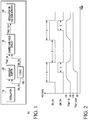
- FIG. 1 is a functional block diagram of a portion of a typical PMC 100, which portion includes circuits that provide a reference voltage.
- the circuits that provide the reference voltage include an oscillator 110 and a bandgap buffer 120, and, if the PMC 100 has a low power mode, may also include a sample-and-hold circuit 130 for sampling and storing the reference voltage, and further include logic 150.
- the oscillator 110 outputs a signal to the bandgap buffer 120.
- the bandgap buffer 120 outputs a reference voltage V REF_IN to the sample-and-hold circuit 130.
- the sample-and-hold circuit 130 outputs a V REF_OUT signal to a functional analog block 140 that can be a regulator, a voltage monitor, or any other analog circuit.
- the logic 150 outputs a bandgap buffer enable signal BG_EN and a switch enable signal SW_EN to the bandgap buffer 120 and to the sample-and-hold circuit 130, respectively.
- the oscillator 110 typically remains on because the oscillator consumes a relatively small amount of power.
- the bandgap buffer 120 is off most of the time to reduce power consumption. This is because the bandgap buffer 120 consumes a relatively large amount of power.
- the sample-and-hold circuit 130 should maintain V REF_OUT at or near the reference voltage.
- FIG. 2 is a graph of a set of signals that may be present in the portion of the typical PMC 100 that provides the reference voltage.
- the bandgap buffer enable signal BG_EN and the switch enable signal SW_EN are digital signals that are either high or low.
- the signals V REF_IN and V REF_OUT are analog signals.
- FIG. 2 suggests that a typical reference voltage is 1.2V; however, other values for the reference voltage are possible.
- the logic 150 in the PMC 100 periodically turns on the bandgap buffer 120 for an interval "A".
- the interval "A" typically ranges from 10 ⁇ s to 40 ⁇ s.
- the bandgap buffer 120 When the bandgap buffer 120 is on, it outputs the reference voltage so that the sample-and-hold circuit 130 can be refreshed during each interval "A".
- Interval "B” is an interval between successive intervals "A”.
- the length of interval “B” of the sample-and-hold circuit 130 is inversely proportional to the overall power consumption of the PMC 100.
- the interval “B” typically ranges from 2ms to 100ms.
- the overall power consumption of the bandgap buffer 120 when the PMC 100 is operating in a low power mode can be estimated by multiplying the power consumption of the bandgap buffer when it is on by number of microseconds that it is on, and then taking into account number of milliseconds that the bandgap buffer is off.
- FIG. 3 is a schematic of a known sample-and-hold circuit 300 of the typical PMC 100.
- the known sample-and-hold circuit 300 includes a capacitor 301. Typically, the capacitor 301 has a value of 10 ⁇ F.
- the known sample-and-hold circuit 300 includes an inverter 309 and one or more transistors 313, 315 and 317.
- the logic 150 of the typical PMC 100 causes the SW_EN signal to go high during each interval "C". When the SW_EN signal is high, transistor 313 is off and transistors 315 and 317 are on. When transistors 315 and 317 are on, capacitor 301 is re-charged such that a voltage across the capacitor 301 is the reference voltage.
- the logic 150 causes the BG_EN signal and the SW_EN signal to go low at the same time.
- the SW_EN signal going low causes the transistors 315 and 317 to turn off.
- Transistor 313 is used to reduce leakage in transistor 315 and transistor 317 ; however, leakage nevertheless occurs at transistor 315 and transistor 317.
- leakage it is meant a current between drain and source terminals of a transistor when the transistor is normally considered to be not conducting. When the transistors 315 and 317 are off, leakage current through transistors 315 and 317 disturbs the charge (and voltage) stored in the capacitor 301, especially at temperatures above approximately 125°C.
- the sample-and-hold circuit 130 When the bandgap buffer 120 is off, the sample-and-hold circuit 130 is able to maintain at its output terminal, for a limited amount of time, a voltage at or near the reference voltage due to the presence of capacitor 301.
- the refresh period "B" of the known sample-and-hold circuit 300 is 2ms to 100ms, depending on a size of the capacitor 301, supply voltage and temperature.
- a longer refresh period "B" requires a larger capacitor 301, but a larger capacitor requires more area which is disadvantageous.
- the known sample-and-hold circuit 300 is disadvantageous because the refresh period "B", which is when the bandgap buffer 120 is off, is relatively short for a given value of the capacitor 301.
- the typical PMC 100 that includes the known sample-and-hold circuit 300 may consume an undesirable amount of power when the typical PMC is in the low power mode. This is because the known sample-and-hold circuit 300 may consume an undesirable amount of power when the typical PMC 100 is in the low power mode.
- the known sample-and-hold circuit 300 may consume an undesirable amount of power when the typical PMC 100 is in the low power mode because the known sample-and-hold circuit must be turned on often.
- the leakage current through transistors 313, 315 and 317 increases.
- the size of capacitor 301 can be increased which is disadvantageous, or a frequency of refresh of capacitor 301 can be increased which is also disadvantageous, or both the size and the frequency can be increased.
- the known sample-and-hold circuit 300 is fabricated using bulk technology, there is a parasitic reverse diode (not shown) across the terminals of transistor 317. The parasitic reverse diode starts to conduct current at high temperatures which causes capacitor 301 to either discharge to ground or to charge to V DD , depending on the polarity of transistor 317.
- the known sample-and-hold circuit 300 As result of a drain-to-source voltage difference in the transistors of the known sample-and-hold circuit 300, leakage readily occurs, especially at high temperatures.
- FD-SOI fully depleted silicon-on-insulator
- the known sample-and-hold circuit 300 still may exhibit excessive leakage due to unwanted conduction across transistor 315 and transistor 317 depending on a size, or channel length, of transistor 315 and transistor 317. For example, when transistor 317 is off, transistor 317 acts as a very large, but not infinite, resistance.
- the known sample-and-hold circuit 300 uses long channel, or larger, transistors.
- the width-to-length ratio of the channel of the transistors used in the known sample-and-hold circuit 300 is 0.2 ⁇ m/5 ⁇ m.
- a switch is split into series switches, and an intermediate node is biased to the output voltage.
- the biasing of the intermediate node is accomplished using a voltage buffer that uses, as its input, an output voltage of the known sample-and-hold circuit.
- use of a buffer to bias the intermediate node increases consumption, die area and circuit complexity.
- a switch is split into series switches, and an intermediate node is biased to a copy of the output, scaled down by a resistor branch.
- this known circuit requires a power-consuming resistor branch (a resistor divider) to generate the bias voltage for the intermediate node of the switch, which limits its application because this known circuit is only worthwhile when an amplifier and a resistor branch already exist; if they do not already exist the area and/or power consumption increases.
- a switch is split into series switches, and the intermediate node is biased to a fixed reference voltage which generates a reduction in the leakage that depends on a value of the charge stored in the capacitor.
- a fixed reference voltage which generates a reduction in the leakage that depends on a value of the charge stored in the capacitor.
- a switch is split into series switches and an intermediate node is biased by a voltage through the use of another switch.
- the bias voltage must be generated from a buffer or through a resistor divider both of which disadvantageously use more power.
- FIG. 4 is a simplified schematic of one embodiment of a sample-and-hold circuit 400 in accordance with the invention.
- the sample-and-hold circuit 400 samples and stores an input voltage.
- the input voltage is a reference voltage.
- the reference voltage is a bandgap voltage.
- the bandgap voltage is 1.2V.
- the sample-and-hold circuit 400 is coupled to a bandgap buffer 120 that consumes about 100 ⁇ A when it is on.
- the bandgap buffer 120 is coupled to a low frequency (about 10Hz) oscillator 110 that consumes about 25nA when it is on.
- the number of milliseconds that the bandgap buffer 120 is off is approximately 1100ms, i.e., the interval "B" is 1100ms, whereas with the known sample-and-hold circuit 300, the number of milliseconds that the bandgap buffer 120 is off is approximately 13ms, considering a reference voltage of 1.2V, a same temperature, and a same amount of voltage degradation at the V REF_OUT terminal of each circuit.
- the sample-and-hold circuit 400 is used in a voltage reference portion of a PMC such as the typical PMC 100.
- the voltage reference should remain precise even when the PMC is operating in low power mode.
- the sample-and-hold circuit 400 in accordance with the invention allows a precise voltage reference to be continuously available when the PMC is operating in the low power mode.
- the sample-and-hold circuit 400 may provide a voltage reference for an analog circuit such as a regulator or a voltage monitor.
- the sample-and-hold circuit 400 consumes less power to maintain the V REF_OUT constant than does the known sample-and-hold circuit 300, while using a same total capacitance. From another perspective, the sample-and-hold circuit 400 allows for use of a smaller total capacitance, while consuming the same power as does the known sample-and-hold circuit 300, to maintain the V REF_OUT constant.
- the sample-and-hold circuit 400 in accordance with the invention does not need to use long channel length transistors.
- the sample-and-hold circuit 400 can advantageously use transistors of almost minimum channel length because the drain-to-source voltage difference of its transistors remains small for longer periods of time.
- the channel of transistors 402, 404 and 406 have a width-to-length ratio of 0.2 ⁇ m/0.25 ⁇ m. Therefore, transistors 402, 404 and 406 do not have long channel lengths. More specifically, transistors 402, 404 and 406 have a smaller drain-to-source voltage difference than transistors 315 and 317 of the known sample-and-hold circuit 300 for a same period of time.
- the sample-and-hold circuit 400 allows the number of milliseconds that the bandgap buffer 120 is off to be advantageously increased (compared to the known sample-and-hold circuit 300 ) while the number of microseconds that the bandgap buffer is on remains unchanged (compared to the known sample-and-hold circuit 300 ).
- the number of milliseconds that the SW_EN signal is low is also increased to match the number of milliseconds that the bandgap buffer 120 is off.
- the SW_EN signal goes high sometime after the bandgap buffer 120 is turned on to assure that the bandgap buffer 120 is fully awake and has entered a stable state when the SW_EN signal is high.
- the sample-and-hold circuit 400 includes transistors 402, 404 and 406.
- a first conducting terminal 401 of transistor 402 is coupled to an input terminal 409 of the sample-and-hold circuit 400.
- a second conducting terminal 403 of transistor 402 is coupled to a first node 411.
- a first intermediate capacitor 421 is coupled between the first node 411 and a ground terminal.
- a first conducting terminal 405 of transistor 404 is coupled to the first node 411.
- a second conducting terminal 407 of transistor 404 is coupled to a second node 412.
- a second intermediate capacitor 422 is coupled between the second node 412 and the ground terminal.
- a first conducting terminal 408 of transistor 406 is coupled to the second node 412.
- a second conducting terminal 410 of transistor 406 is coupled to an output terminal 435 of the sample-and-hold circuit 400.
- a hold capacitor 430 is coupled between the output terminal 435 of the sample-and-hold circuit 400 and ground.
- the capacitance of the first intermediate capacitor 421 is one-tenth the capacitance of the hold capacitor 430
- the capacitance of the second intermediate capacitor 422 is also one-tenth the capacitance of the hold capacitor.
- Transistors 402, 404 and 406 function as switches. These switches are closed when these transistors are on.
- transistors 402, 404 and 406 are PMOS transistors.
- the control terminal of transistors 402, 404 and 406 is coupled to a switch enable terminal 445 of the sample-and-hold circuit 400 through an inverter 440.
- transistors 402, 404 and 406 are NMOS transistors, and, in such embodiment, the inverter 440 is not included in the circuit and the control terminal of transistors 402, 404 and 406 is coupled directly to the switch enable terminal 445.
- Transistors 402, 404 and 406 are turned on and off simultaneously by the SW_EN signal.
- a voltage at the first node 411 and the second node 412 is V REF_IN .
- transistors 402, 404 and 406 are on, and the first intermediate capacitor 421, the second intermediate capacitor 422 and the hold capacitor 430 are charged to V REF_IN .
- the configuration of the sample-and-hold circuit 400 allows V DS of transistors 402, 404 and 406 to remain near 0V for as long as possible. More specifically, the presence of the first intermediate capacitor 421 and the second intermediate capacitor 422 in the sample-and-hold circuit 400 allows V DS of transistors 402, 404 and 406 to remain near 0V for longer than V DS of corresponding transistors in the known sample-and-hold circuit 300.
- the reference voltage is present at the output of the bandgap buffer 120.
- the bandgap buffer 120 is off, the output of the bandgap buffer 120 is grounded.
- the BG_EN signal is high the bandgap buffer 120 is on, and the output of the bandgap buffer 120 is the reference voltage.
- the sample-and-hold circuit 400 is refreshed, and the voltage at the first node 411, at the second node 412 and at the output terminal 435 of the sample-and-hold circuit are initially at the reference voltage.
- the bandgap buffer 120 is turned off, the voltage V REF _ IN goes to 0V.
- the logic 150 causes the SW_EN signal to go low at the same time that the logic causes the BG_EN signal to go low.
- the voltage at the first intermediate node 411 remains at V REF_IN for a while.
- a higher voltage initially V REF_IN
- current flows through transistor 402 in spite of it being off.
- This current discharges the first intermediate capacitor 421, and, as a result, the voltage at the first intermediate node 411 goes down from its initial value od V REF_IN .
- This current flows through transistor 402 to a ground terminal within the bandgap buffer 120.
- the voltage at the first intermediate node 411 is decreasing, the voltage at the first conducting terminal 405 of transistor 404 decreases from its initial value of V REF_IN .
- the voltage at the first conducting terminal 405 of transistor 404 being less than V REF_IN while the voltage at the second conducting terminal 407 of transistor 404 is higher (initially V REF_IN )
- V REF_IN the voltage at the second conducting terminal 407 of transistor 404 is higher (initially V REF_IN )
- V DS across transistor 404 As a result of the voltage V DS across transistor 404, a current flows through transistor 404 in spite of transistor 404 being off. This current discharges the second intermediate capacitor 422, and, as a result, the voltage at the second intermediate node 412 goes down from its initial value of V REF_IN .
- the voltage at the second intermediate node 412 is decreasing, the voltage at the first conducting terminal 408 of transistor 406 decreases from its initial value of V REF_IN .
- the voltage at the first conducting terminal 408 of transistor 406 being less than V REF_IN while the voltage at the second conducting terminal 410 of transistor 406 is higher (initially V REF_IN )
- V REF_IN there is a voltage V DS across transistor 406.
- the voltage V DS across transistor 406 current flows through transistor 406 in spite of transistor 406 being off. This current discharges the hold capacitor 430, and, as a result, the voltage at the output of the known sample-and-hold circuit 400 goes down from its initial value of V REF_IN .
- the voltage V REF_OUT at the output of the sample-and-hold circuit 400 may go to 0V unless the sample-and-hold circuit 400 is refreshed.
- the sample-and-hold circuit 400 maintains the V DS of transistor 406 closer to 0V for a longer period than the known sample-and-hold circuit 300 maintains V DS of its corresponding transistor 317.
- the hold capacitor 430 starts to discharge only after the second intermediate capacitor 422 has been discharging for a while.
- the second intermediate capacitor 422 starts to only after the first intermediate capacitor 421 has been discharging for a while. Note that the first intermediate capacitor 421 and the second intermediate capacitor 422 may be smaller than the hold capacitor 430, and, therefore, individually discharge faster than the hold capacitor 430 discharges.
- the presence of the first intermediate capacitor 421 and the second intermediate capacitor 422 nevertheless substantially delays discharge of the hold capacitor 430.
- the output voltage V REF_OUT of the sample-and-hold circuit 400 is maintained at or near V REF_IN for a longer time than with the known sample-and-hold circuit 300.
- the sample-and-hold circuit 400 does not include transistor 404, the second intermediate node 412 and the second intermediate capacitor 422.
- FIG. 5 is a simplified schematic of a multiple-stage implementation of a sample-and-hold circuit 500.
- the sample-and-hold circuit 500 includes one or more additional transistors, and a corresponding number of additional intermediate capacitors coupled between a corresponding number of additional intermediate nodes and ground.
- one additional transistor 508 is added, one additional node 513 is defined and one additional intermediate capacitor 523 is added.
- An advantage of the multiple-stage implementation of the sample-and-hold circuit 500 is the reduction of leakage.
- the sample-and-hold circuits 400 and 500 which are constructed using PMOS transistors, function well provided that the reference voltage is not near ground. However, if the reference voltage were near ground, it may be difficult to turn on the PMOS transistors when trying to refresh hold capacitor 430. In such case, the sample-and-hold circuits 400 and 500 can be constructed using NMOS transistors instead of using PMOS transistors. Embodiments of the sample-and-hold circuits 400 and 500 constructed using NMOS transistors function well provided that the reference voltage is not near V DD . However, if the reference voltage were near V DD , it may be difficult to turn on the NMOS transistors when trying to refresh hold capacitor 430.
- the sample-and-hold circuit 600 shown in FIG. 6 functions well. With the sample-and-hold circuit 600, one of the set of PMOS transistors and the set of NMOS transistors turns on regardless of whether the reference voltage is near V DD or near ground.
- the NMOS transistors and the capacitors coupled to them in FIG. 6 are configured analogously to the way in which the PMOS transistors and the capacitors coupled to them are configured in FIG. 4 and FIG. 5 ; therefore, there is no need to describe their configuration in detail.
- FIG. 6 shows that each transistor of the sample-and-hold circuit 500 can be replaced with a transmission gate.
- the sample-and-hold circuit 400 includes very low leakage switches (transistors 402, 404 and 406 ) capable of a holding a sampled voltage for a longer period than can the known sample-and-hold circuit 300.
- the switches can be built without using long channel devices. When the switches are built without using long channel devices settling time is improved. Because there is no device connecting V DD to the first intermediate node 411 or to the second intermediate node 412, the leakage between the input terminal 409 and the output terminal 435 of the sample-and-hold circuit 400 is highly reduced.
- Leakage caused by a voltage difference between a drain terminal and a source terminal in a CMOS transistor operating as a switch is substantially reduced using at least one intermediate capacitor (such as first intermediate capacitor 421 ) connected to a respective at least one intermediate node, without the need of a buffer.
- at least one intermediate capacitor such as first intermediate capacitor 421
- the reference voltage outputted by the sample-and-hold circuit 400, 500 and 600 is precise even when the PMC 100 is operating in the low power mode.
- the circuit in accordance with the invention is fabricated using FD-SOI technology.
- FD-SOI technology there are parasitic diodes at the terminals of transistors 402, 404 and 406 that tend to discharge the hold capacitor 430.
- a low power consumption bandgap buffer is typically less precise that a high power consumption bandgap buffer.
- the sample-and-hold circuit 400 is particularly advantageous when used in a PMC that lacks a low power consumption bandgap buffer and has only a high power consumption bandgap buffer such as a bandgap buffer that consumes 100 ⁇ A.
- the sample-and-hold circuit 400 uses approximately the same amount of capacitance (die area) that is used by the known sample-and-hold circuit 300 but distributed in a different manner.
- the value of capacitor 301 of the known sample-and-hold circuit 300 is 10 ⁇ F.
- the value of hold capacitor 430 is 8pF
- the value of first intermediate capacitor 421 is 0.8 ⁇ F
- the value of second intermediate capacitor 422 is 0.8 ⁇ F. Consequently, the total capacitance of the capacitors used in the sample-and-hold circuit 400 in accordance with the invention is advantageously approximately the same as the total capacitance of the capacitor used in the known sample-and-hold circuit 300.
- Embodiments may include features recited in the following numbered clauses:
- a sample-and-hold circuit which includes a hold capacitor at its output terminal and at least one intermediate capacitor, intermittently receives an input voltage, and a first value of a switch enable signal causes the sample-and-hold circuit to sample the input voltage and to charge the at least one intermediate capacitor and the hold capacitor to the input voltage, and when it is not receiving the input voltage, a second value of the switch enable signal causes the sample-and-hold circuit to hold, at its output terminal, the input voltage until the hold capacitor discharges, which starts to discharge only after the at least one intermediate capacitor has substantially discharged.
- Coupled is defined as “connected”, and encompasses the coupling of devices that may be physically, electrically or communicatively connected, although the coupling may not necessarily be directly, and not necessarily be mechanically.
- Configured to describes hardware, software or a combination of hardware and software that is adapted to, set up, arranged, built, composed, constructed, designed or that has any combination of these characteristics to carry out a given function.
- adapted to describes hardware, software or a combination of hardware and software that is capable of, able to accommodate, to make, or that is suitable to carry out a given function.
- Coupled is not intended to be limited to a direct coupling or a mechanical coupling, and that one or more additional elements may be interposed between two elements that are coupled. It is understood that the terms so used are interchangeable under appropriate circumstances such that the embodiments of the invention described herein are, for example, capable of operation in other orientations than those illustrated or otherwise described herein.
Landscapes
- Engineering & Computer Science (AREA)
- Microelectronics & Electronic Packaging (AREA)
- Physics & Mathematics (AREA)
- Nonlinear Science (AREA)
- Electromagnetism (AREA)
- General Physics & Mathematics (AREA)
- Radar, Positioning & Navigation (AREA)
- Automation & Control Theory (AREA)
- Analogue/Digital Conversion (AREA)
Abstract
Description
- This invention relates generally to electronic circuits, and more specifically to power management controllers.
- When a Power Management Controller (PMC) of a System on a Chip (SoC) is operating in a low power mode, most of its circuits are off most of the time to reduce power consumption. A PMC may include a portion that provides a reference voltage. The reference voltage should be precise even when the PMC is operating in the low power mode.
- The present invention is illustrated by way of example and is not limited by the accompanying figures, in which like references indicate similar elements. Elements in the figures are illustrated for simplicity and clarity and have not necessarily been drawn to scale.
-
FIG. 1 is a functional block diagram of a portion of a typical PMC. -
FIG. 2 is a graph of a set of signals in the portion of the typical PMC ofFIG. 1 . -
FIG. 3 is a schematic of a known sample-and-hold circuit. -
FIG. 4 is a simplified schematic of one embodiment of a sample-and-hold circuit in accordance with the invention. -
FIG. 5 is a simplified schematic of another embodiment of a sample-and-hold circuit in accordance with the invention. -
FIG. 6 is a simplified schematic of still another embodiment of a sample-and-hold circuit in accordance with the invention. -
FIG. 1 is a functional block diagram of a portion of atypical PMC 100, which portion includes circuits that provide a reference voltage. The circuits that provide the reference voltage include anoscillator 110 and abandgap buffer 120, and, if thePMC 100 has a low power mode, may also include a sample-and-hold circuit 130 for sampling and storing the reference voltage, and further includelogic 150. Theoscillator 110 outputs a signal to thebandgap buffer 120. Thebandgap buffer 120 outputs a reference voltage VREF_IN to the sample-and-hold circuit 130. The sample-and-hold circuit 130 outputs a VREF_OUT signal to a functionalanalog block 140 that can be a regulator, a voltage monitor, or any other analog circuit. Thelogic 150 outputs a bandgap buffer enable signal BG_EN and a switch enable signal SW_EN to thebandgap buffer 120 and to the sample-and-hold circuit 130, respectively. When thePMC 100 is operating in a low power mode, theoscillator 110 typically remains on because the oscillator consumes a relatively small amount of power. When thePMC 100 is operating in a low power mode, thebandgap buffer 120 is off most of the time to reduce power consumption. This is because thebandgap buffer 120 consumes a relatively large amount of power. When thebandgap buffer 120 is off, the sample-and-hold circuit 130 should maintain VREF_OUT at or near the reference voltage. -
FIG. 2 is a graph of a set of signals that may be present in the portion of thetypical PMC 100 that provides the reference voltage. The bandgap buffer enable signal BG_EN and the switch enable signal SW_EN are digital signals that are either high or low. The signals VREF_IN and VREF_OUT are analog signals.FIG. 2 suggests that a typical reference voltage is 1.2V; however, other values for the reference voltage are possible. Thelogic 150 in thePMC 100 periodically turns on thebandgap buffer 120 for an interval "A". The interval "A" typically ranges from 10µs to 40µs. When thebandgap buffer 120 is on, it outputs the reference voltage so that the sample-and-hold circuit 130 can be refreshed during each interval "A". Interval "B" is an interval between successive intervals "A". The length of interval "B" of the sample-and-hold circuit 130 is inversely proportional to the overall power consumption of thePMC 100. The interval "B" typically ranges from 2ms to 100ms. - The overall power consumption of the
bandgap buffer 120 when thePMC 100 is operating in a low power mode can be estimated by multiplying the power consumption of the bandgap buffer when it is on by number of microseconds that it is on, and then taking into account number of milliseconds that the bandgap buffer is off. -
FIG. 3 is a schematic of a known sample-and-hold circuit 300 of thetypical PMC 100. The known sample-and-hold circuit 300 includes acapacitor 301. Typically, thecapacitor 301 has a value of 10ρF. The known sample-and-hold circuit 300 includes aninverter 309 and one ormore transistors logic 150 of thetypical PMC 100 causes the SW_EN signal to go high during each interval "C". When the SW_EN signal is high,transistor 313 is off andtransistors transistors capacitor 301 is re-charged such that a voltage across thecapacitor 301 is the reference voltage. Thelogic 150 causes the BG_EN signal and the SW_EN signal to go low at the same time. The SW_EN signal going low causes thetransistors Transistor 313 is used to reduce leakage intransistor 315 andtransistor 317; however, leakage nevertheless occurs attransistor 315 andtransistor 317. By "leakage" it is meant a current between drain and source terminals of a transistor when the transistor is normally considered to be not conducting. When thetransistors transistors capacitor 301, especially at temperatures above approximately 125°C. When thebandgap buffer 120 is off, the sample-and-hold circuit 130 is able to maintain at its output terminal, for a limited amount of time, a voltage at or near the reference voltage due to the presence ofcapacitor 301. Thelonger capacitor 301 can maintain its voltage the longer is the refresh period "B" of the known sample-and-hold circuit 300, and, as a result, the lower is the overall consumption of thePMC 100. The refresh period "B" of the known sample-and-hold circuit 300 is 2ms to 100ms, depending on a size of thecapacitor 301, supply voltage and temperature. However, with the known sample-and-hold circuit 300, a longer refresh period "B" requires alarger capacitor 301, but a larger capacitor requires more area which is disadvantageous. The known sample-and-hold circuit 300 is disadvantageous because the refresh period "B", which is when thebandgap buffer 120 is off, is relatively short for a given value of thecapacitor 301. As a result, thetypical PMC 100 that includes the known sample-and-hold circuit 300 may consume an undesirable amount of power when the typical PMC is in the low power mode. This is because the known sample-and-hold circuit 300 may consume an undesirable amount of power when thetypical PMC 100 is in the low power mode. The known sample-and-hold circuit 300 may consume an undesirable amount of power when thetypical PMC 100 is in the low power mode because the known sample-and-hold circuit must be turned on often. - As the geometry of the fabrication process by which the known sample-and-
hold circuit 300 is constructed becomes smaller, the leakage current throughtransistors capacitor 301 can be increased which is disadvantageous, or a frequency of refresh ofcapacitor 301 can be increased which is also disadvantageous, or both the size and the frequency can be increased. When the known sample-and-hold circuit 300 is fabricated using bulk technology, there is a parasitic reverse diode (not shown) across the terminals oftransistor 317. The parasitic reverse diode starts to conduct current at high temperatures which causescapacitor 301 to either discharge to ground or to charge to VDD, depending on the polarity oftransistor 317. As result of a drain-to-source voltage difference in the transistors of the known sample-and-hold circuit 300, leakage readily occurs, especially at high temperatures. When the known sample-and-hold circuit 300 is fabricated using fully depleted silicon-on-insulator (FD-SOI) technology, such parasitic reverse diode is not present; however, the known sample-and-hold circuit still may exhibit excessive leakage due to unwanted conduction acrosstransistor 315 andtransistor 317 depending on a size, or channel length, oftransistor 315 andtransistor 317. For example, whentransistor 317 is off,transistor 317 acts as a very large, but not infinite, resistance. As a result, a small current flows from the VDD terminal tocapacitor 301, and VREF_OUT slowly ramps up untiltransistor 317 is turned on to refresh VREF_OUT to the reference voltage. A similar, but opposite, effect occurs iftransistor 313 is connected to the ground terminal instead of VDD terminal. In an attempt to reduce such leakage, the known sample-and-hold circuit 300 uses long channel, or larger, transistors. For example, the width-to-length ratio of the channel of the transistors used in the known sample-and-hold circuit 300 is 0.2µm/5µm. - In another known sample-and-hold circuit, a switch is split into series switches, and an intermediate node is biased to the output voltage. The biasing of the intermediate node is accomplished using a voltage buffer that uses, as its input, an output voltage of the known sample-and-hold circuit. Disadvantageously, use of a buffer to bias the intermediate node increases consumption, die area and circuit complexity.
- In yet known sample-and-hold circuit, a switch is split into series switches, and an intermediate node is biased to a copy of the output, scaled down by a resistor branch. Disadvantageously, this known circuit requires a power-consuming resistor branch (a resistor divider) to generate the bias voltage for the intermediate node of the switch, which limits its application because this known circuit is only worthwhile when an amplifier and a resistor branch already exist; if they do not already exist the area and/or power consumption increases.
- In still another known sample-and-hold circuit, a switch is split into series switches, and the intermediate node is biased to a fixed reference voltage which generates a reduction in the leakage that depends on a value of the charge stored in the capacitor. However, the use of a continuous fixed reference voltage requires a circuit that is always consuming power, which increases consumption and complexity.
- In a further known sample-and-hold circuit, a switch is split into series switches and an intermediate node is biased by a voltage through the use of another switch. The bias voltage must be generated from a buffer or through a resistor divider both of which disadvantageously use more power.
-
FIG. 4 is a simplified schematic of one embodiment of a sample-and-hold circuit 400 in accordance with the invention. The sample-and-hold circuit 400 samples and stores an input voltage. In one embodiment, the input voltage is a reference voltage. In one embodiment, the reference voltage is a bandgap voltage. In one embodiment the bandgap voltage is 1.2V. The sample-and-hold circuit 400 is coupled to abandgap buffer 120 that consumes about 100µA when it is on. Thebandgap buffer 120 is coupled to a low frequency (about 10Hz)oscillator 110 that consumes about 25nA when it is on. - Referring again to
FIG. 2 , with the sample-and-hold circuit 400, the number of milliseconds that thebandgap buffer 120 is off is approximately 1100ms, i.e., the interval "B" is 1100ms, whereas with the known sample-and-hold circuit 300, the number of milliseconds that thebandgap buffer 120 is off is approximately 13ms, considering a reference voltage of 1.2V, a same temperature, and a same amount of voltage degradation at the VREF_OUT terminal of each circuit. - In one embodiment, the sample-and-
hold circuit 400 is used in a voltage reference portion of a PMC such as thetypical PMC 100. The voltage reference should remain precise even when the PMC is operating in low power mode. The sample-and-hold circuit 400 in accordance with the invention allows a precise voltage reference to be continuously available when the PMC is operating in the low power mode. The sample-and-hold circuit 400 may provide a voltage reference for an analog circuit such as a regulator or a voltage monitor. - From one perspective, the sample-and-
hold circuit 400 consumes less power to maintain the VREF_OUT constant than does the known sample-and-hold circuit 300, while using a same total capacitance. From another perspective, the sample-and-hold circuit 400 allows for use of a smaller total capacitance, while consuming the same power as does the known sample-and-hold circuit 300, to maintain the VREF_OUT constant. - Unlike the known sample-and-
hold circuit 300, the sample-and-hold circuit 400 in accordance with the invention does not need to use long channel length transistors. The sample-and-hold circuit 400 can advantageously use transistors of almost minimum channel length because the drain-to-source voltage difference of its transistors remains small for longer periods of time. In one embodiment, the channel oftransistors transistors transistors transistors hold circuit 300 for a same period of time. - With the sample-and-
hold circuit 400, there is, advantageously, minimal current flowing into or out of thehold capacitor 430 during interval "B". As a result, during interval "B", the sample-and-hold circuit 400 holds VREF_OUT nearly constant. - The sample-and-
hold circuit 400 allows the number of milliseconds that thebandgap buffer 120 is off to be advantageously increased (compared to the known sample-and-hold circuit 300) while the number of microseconds that the bandgap buffer is on remains unchanged (compared to the known sample-and-hold circuit 300). - With the sample-and-
hold circuit 400, the number of milliseconds that the SW_EN signal is low is also increased to match the number of milliseconds that thebandgap buffer 120 is off. The SW_EN signal goes high sometime after thebandgap buffer 120 is turned on to assure that thebandgap buffer 120 is fully awake and has entered a stable state when the SW_EN signal is high. - The sample-and-
hold circuit 400 includestransistors first conducting terminal 401 oftransistor 402 is coupled to aninput terminal 409 of the sample-and-hold circuit 400. Asecond conducting terminal 403 oftransistor 402 is coupled to afirst node 411. A firstintermediate capacitor 421 is coupled between thefirst node 411 and a ground terminal. Afirst conducting terminal 405 oftransistor 404 is coupled to thefirst node 411. Asecond conducting terminal 407 oftransistor 404 is coupled to asecond node 412. A secondintermediate capacitor 422 is coupled between thesecond node 412 and the ground terminal. Afirst conducting terminal 408 oftransistor 406 is coupled to thesecond node 412. Asecond conducting terminal 410 oftransistor 406 is coupled to anoutput terminal 435 of the sample-and-hold circuit 400. Ahold capacitor 430 is coupled between theoutput terminal 435 of the sample-and-hold circuit 400 and ground. In one embodiment, the capacitance of the firstintermediate capacitor 421 is one-tenth the capacitance of thehold capacitor 430, and the capacitance of the secondintermediate capacitor 422 is also one-tenth the capacitance of the hold capacitor. -
Transistors transistors transistors terminal 445 of the sample-and-hold circuit 400 through aninverter 440. In another embodiment (not shown),transistors inverter 440 is not included in the circuit and the control terminal oftransistors terminal 445.Transistors transistors first node 411 and thesecond node 412 is VREF_IN. Whentransistors intermediate capacitor 421, the secondintermediate capacitor 422 and thehold capacitor 430 are charged to VREF_IN. The configuration of the sample-and-hold circuit 400 allows VDS oftransistors intermediate capacitor 421 and the secondintermediate capacitor 422 in the sample-and-hold circuit 400 allows VDS oftransistors hold circuit 300. - When the
bandgap buffer 120 is on, the reference voltage is present at the output of thebandgap buffer 120. When thebandgap buffer 120 is off, the output of thebandgap buffer 120 is grounded. When the BG_EN signal is high thebandgap buffer 120 is on, and the output of thebandgap buffer 120 is the reference voltage. When the output of thebandgap buffer 120 is the reference voltage and the SW_EN signal is high, the sample-and-hold circuit 400 is refreshed, and the voltage at thefirst node 411, at thesecond node 412 and at theoutput terminal 435 of the sample-and-hold circuit are initially at the reference voltage. When thebandgap buffer 120 is turned off, the voltage VREF_IN goes to 0V. Thelogic 150 causes the SW_EN signal to go low at the same time that the logic causes the BG_EN signal to go low. - However, the voltage at the first
intermediate node 411 remains at VREF_IN for a while. As a result of 0V being present at the first conductingterminal 401 oftransistor 402 while a higher voltage (initially VREF_IN) is at thesecond conducting terminal 403 oftransistor 402 there is a voltage VDS acrosstransistor 402. As a result of the voltage VDS acrosstransistor 402, current flows throughtransistor 402 in spite of it being off. This current discharges the firstintermediate capacitor 421, and, as a result, the voltage at the firstintermediate node 411 goes down from its initial value od VREF_IN. This current flows throughtransistor 402 to a ground terminal within thebandgap buffer 120. - Because the voltage at the first
intermediate node 411 is decreasing, the voltage at the first conductingterminal 405 oftransistor 404 decreases from its initial value of VREF_IN. As a result of the voltage at the first conductingterminal 405 oftransistor 404 being less than VREF_IN while the voltage at thesecond conducting terminal 407 oftransistor 404 is higher (initially VREF_IN), there is an increasing voltage VDS acrosstransistor 404. As a result of the voltage VDS acrosstransistor 404, a current flows throughtransistor 404 in spite oftransistor 404 being off. This current discharges the secondintermediate capacitor 422, and, as a result, the voltage at the secondintermediate node 412 goes down from its initial value of VREF_IN. - Because the voltage at the second
intermediate node 412 is decreasing, the voltage at the first conductingterminal 408 oftransistor 406 decreases from its initial value of VREF_IN. As a result of the voltage at the first conductingterminal 408 oftransistor 406 being less than VREF_IN while the voltage at thesecond conducting terminal 410 oftransistor 406 is higher (initially VREF_IN), there is a voltage VDS acrosstransistor 406. As a result of the voltage VDS acrosstransistor 406, current flows throughtransistor 406 in spite oftransistor 406 being off. This current discharges thehold capacitor 430, and, as a result, the voltage at the output of the known sample-and-hold circuit 400 goes down from its initial value of VREF_IN. Eventually, the voltage VREF_OUT at the output of the sample-and-hold circuit 400 may go to 0V unless the sample-and-hold circuit 400 is refreshed. Advantageously, the sample-and-hold circuit 400 maintains the VDS oftransistor 406 closer to 0V for a longer period than the known sample-and-hold circuit 300 maintains VDS of itscorresponding transistor 317. Thehold capacitor 430 starts to discharge only after the secondintermediate capacitor 422 has been discharging for a while. Furthermore, the secondintermediate capacitor 422 starts to only after the firstintermediate capacitor 421 has been discharging for a while. Note that the firstintermediate capacitor 421 and the secondintermediate capacitor 422 may be smaller than thehold capacitor 430, and, therefore, individually discharge faster than thehold capacitor 430 discharges. However, the presence of the firstintermediate capacitor 421 and the secondintermediate capacitor 422 nevertheless substantially delays discharge of thehold capacitor 430. As a result of the presence of the firstintermediate capacitor 421 and the secondintermediate capacitor 422, the output voltage VREF_OUT of the sample-and-hold circuit 400 is maintained at or near VREF_IN for a longer time than with the known sample-and-hold circuit 300. - In another embodiment (not shown), the sample-and-
hold circuit 400 does not includetransistor 404, the secondintermediate node 412 and the secondintermediate capacitor 422. -
FIG. 5 is a simplified schematic of a multiple-stage implementation of a sample-and-hold circuit 500. Compared to the sample-and-hold circuit 400, the sample-and-hold circuit 500 includes one or more additional transistors, and a corresponding number of additional intermediate capacitors coupled between a corresponding number of additional intermediate nodes and ground. In the illustrated embodiment, oneadditional transistor 508 is added, oneadditional node 513 is defined and one additionalintermediate capacitor 523 is added. An advantage of the multiple-stage implementation of the sample-and-hold circuit 500 is the reduction of leakage. - The sample-and-
hold circuits hold capacitor 430. In such case, the sample-and-hold circuits hold circuits hold capacitor 430. - If the range of the reference voltage is uncertain, i.e., it is not known whether is the reference voltage near ground or near VDD, then the sample-and-
hold circuit 600 shown inFIG. 6 functions well. With the sample-and-hold circuit 600, one of the set of PMOS transistors and the set of NMOS transistors turns on regardless of whether the reference voltage is near VDD or near ground. The NMOS transistors and the capacitors coupled to them inFIG. 6 are configured analogously to the way in which the PMOS transistors and the capacitors coupled to them are configured inFIG. 4 andFIG. 5 ; therefore, there is no need to describe their configuration in detail.FIG. 6 shows that each transistor of the sample-and-hold circuit 500 can be replaced with a transmission gate. - The sample-and-
hold circuit 400 includes very low leakage switches (transistors hold circuit 300. Advantageously, the switches (transistors intermediate node 411 or to the secondintermediate node 412, the leakage between theinput terminal 409 and theoutput terminal 435 of the sample-and-hold circuit 400 is highly reduced. - Leakage caused by a voltage difference between a drain terminal and a source terminal in a CMOS transistor operating as a switch is substantially reduced using at least one intermediate capacitor (such as first intermediate capacitor 421) connected to a respective at least one intermediate node, without the need of a buffer.
- Advantageously, the reference voltage outputted by the sample-and-
hold circuit PMC 100 is operating in the low power mode. - As interval "B" (see
FIG. 2 ) is doubled, power consumption of the portion of thePMC 100 that provides the reference voltage is approximately divided by two, disregarding circuits, such as theoscillator 110, that are always enabled. - In one embodiment, the circuit in accordance with the invention is fabricated using FD-SOI technology. With FD-SOI technology, there are parasitic diodes at the terminals of
transistors hold capacitor 430. - A low power consumption bandgap buffer is typically less precise that a high power consumption bandgap buffer. The sample-and-
hold circuit 400 is particularly advantageous when used in a PMC that lacks a low power consumption bandgap buffer and has only a high power consumption bandgap buffer such as a bandgap buffer that consumes 100µA. - The sample-and-
hold circuit 400 uses approximately the same amount of capacitance (die area) that is used by the known sample-and-hold circuit 300 but distributed in a different manner. For example, the value ofcapacitor 301 of the known sample-and-hold circuit 300 is 10ρF. In one embodiment of the sample-and-hold circuit 400 in accordance with the invention, the value ofhold capacitor 430 is 8pF, the value of firstintermediate capacitor 421 is 0.8ρF and the value of secondintermediate capacitor 422 is 0.8ρF. Consequently, the total capacitance of the capacitors used in the sample-and-hold circuit 400 in accordance with the invention is advantageously approximately the same as the total capacitance of the capacitor used in the known sample-and-hold circuit 300.
Embodiments may include features recited in the following numbered clauses: - 1. A sample-and-hold circuit comprising: a switch enable terminal for receiving a switch enable signal; an input terminal for intermittently receiving an input voltage; a first transistor having one conducting terminal coupled to the input terminal, having another conducting terminal coupled to a node and having a control terminal coupled to the switch enable terminal; an intermediate capacitor coupled between the node and a ground terminal; a second transistor having one conducting terminal coupled to the node, having another conducting terminal coupled to an output terminal and having a control terminal coupled to the switch enable terminal; and a hold capacitor coupled between the output terminal and the ground terminal, wherein, when the input terminal is receiving the input voltage, a first value of the switch enable signal causes the sample-and-hold circuit to sample the input voltage and to charge the intermediate capacitor and the hold capacitor to the sampled input voltage, wherein, when the input terminal is not receiving the input voltage, a second value of the switch enable signal causes the sample-and-hold circuit to hold, at the output terminal, the sampled input voltage until the hold capacitor discharges, and wherein the charge on the intermediate capacitor delays discharging of the hold capacitor.
- 2. The sample-and-hold circuit of clause 1, wherein when the input terminal is receiving the input voltage, the first value of the switch enable signal causes the first transistor and the second transistor to conduct thereby charging the intermediate capacitor and the hold capacitor to the sampled input voltage.
- 3. The sample-and-hold circuit of clause 1, wherein the second value of the switch enable signal causes the first transistor and the second transistor to not conduct except for leakage current.
- 4. The sample-and-hold circuit of clause 3, wherein, when the input terminal is not receiving the input voltage, the input terminal is coupled to ground potential.
- 5. The sample-and-hold circuit of clause 4, wherein, the leakage current causes the charge on the hold capacitor to start discharging only after the intermediate capacitor has substantially discharged.
- 6. The sample-and-hold circuit of clause 1, wherein, the input voltage is a bandgap reference voltage.
- 7. A power management controller comprising: a bandgap buffer configured to intermittently output a reference voltage; a sample-and-hold circuit coupled to the bandgap buffer; and logic configured to output a bandgap buffer enable signal to the bandgap buffer and to output a switch enable signal to the sample-and-hold circuit, wherein the sample-and-hold circuit includes: a switch enable terminal configured to receive the switch enable signal; an input terminal configured to receive the reference voltage; a first transistor having one conducting terminal coupled to the input terminal, another conducting terminal coupled to a node and a control terminal coupled to the switch enable terminal; an intermediate capacitor coupled between the node and a ground terminal; a second transistor having one conducting terminal coupled to the node, another conducting terminal coupled to an output terminal and a control terminal coupled to the switch enable terminal; and a hold capacitor coupled between the output terminal and the ground terminal, wherein, when the input terminal is receiving the reference voltage, a first value of the switch enable signal causes the sample-and-hold circuit to sample the reference voltage and to charge the intermediate capacitor and the hold capacitor to the reference voltage, wherein, when the input terminal is not receiving the reference voltage, a second value of the switch enable signal causes the sample-and-hold circuit to hold, at the output terminal, the reference voltage until the hold capacitor discharges, wherein the charge on the intermediate capacitor delays discharging of the hold capacitor.
- 8. The power management controller of clause 7, including: an oscillator coupled to the bandgap buffer.
- 9. The power management controller of clause 8, including: a regulator coupled to the output terminal of the sample-and-hold circuit.
- 10. The power management controller of clause 8, including:
- a voltage monitor coupled to the output terminal of the sample-and-hold circuit.
- 11. The power management controller of clause 7, wherein when the input terminal is receiving the reference voltage, the first value of the switch enable signal causes the first transistor and the second transistor to conduct thereby charging the intermediate capacitor and the hold capacitor to the reference voltage.
- 12. The power management controller of clause 7, wherein the second value of the switch enable signal causes the first transistor and the second transistor to not conduct except for leakage current.
- 13. The power management controller of clause 12, wherein, when the input terminal is not receiving the reference voltage, the input terminal is coupled to ground potential.
- 14. The power management controller of clause 13, wherein, the leakage current causes the charge on the hold capacitor to start discharging only after the intermediate capacitor has substantially discharged.
- 15. A method with a sample-and-hold circuit having a switch enable terminal coupled to a control terminal of a first transistor, a control terminal of a second transistor and a control terminal of a third transistor, comprising: for a first interval, receiving a reference voltage at an input terminal; during at least some of the first interval, receiving a first value of a switch enable signal at the switch enable terminal, thereby: turning on the first transistor which has one conducting terminal coupled to the input terminal and another conducting terminal coupled to a first node, charging a first intermediate capacitor coupled between the first node and ground turning on the second transistor which has one conducting terminal coupled to the first node and another conducting terminal coupled to a second node, charging a second intermediate capacitor coupled between the second node and ground, turning on the third transistor which has one conducting terminal coupled to the second node and another conducting terminal coupled to an output terminal, and charging a hold capacitor coupled between the output terminal and ground; and during a second interval occurring immediately subsequent to the first interval, cease receiving the reference voltage, and begin receiving a second value of the switch enable signal, thereby: turning off the first transistor, turning off the second transistor, and turning off the third transistor, wherein the charge on the second intermediate capacitor delays discharging of the hold capacitor when the input terminal is not receiving the reference voltage.
- 16. The method of clause 15, wherein, when the input terminal is not receiving the reference voltage, coupling the input terminal to ground potential.
- 17. The method of clause 15, wherein a charge on the first intermediate capacitor delays discharging of the second intermediate capacitor when the input terminal is not receiving the reference voltage.
- 18. The method of clause 15, wherein when the input terminal is receiving the reference voltage, the first value of the switch enable signal causes the first transistor, the second transistor and the third transistor to conduct thereby charging the first intermediate capacitor, the second intermediate capacitor and the hold capacitor to the reference voltage.
- 19. The method of clause 15, wherein the second value of the switch enable signal causes the first transistor, the second transistor and the third transistor to not conduct except for leakage current.
- 20. The method of clause 19, wherein, the leakage current causes the charge on the hold capacitor to start discharging only after the second intermediate capacitor has substantially discharged.
- A sample-and-hold circuit is described which includes a hold capacitor at its output terminal and at least one intermediate capacitor, intermittently receives an input voltage, and a first value of a switch enable signal causes the sample-and-hold circuit to sample the input voltage and to charge the at least one intermediate capacitor and the hold capacitor to the input voltage, and when it is not receiving the input voltage, a second value of the switch enable signal causes the sample-and-hold circuit to hold, at its output terminal, the input voltage until the hold capacitor discharges, which starts to discharge only after the at least one intermediate capacitor has substantially discharged.
- The term "coupled", as used herein, is defined as "connected", and encompasses the coupling of devices that may be physically, electrically or communicatively connected, although the coupling may not necessarily be directly, and not necessarily be mechanically. The term "configured to" describes hardware, software or a combination of hardware and software that is adapted to, set up, arranged, built, composed, constructed, designed or that has any combination of these characteristics to carry out a given function. The term "adapted to" describes hardware, software or a combination of hardware and software that is capable of, able to accommodate, to make, or that is suitable to carry out a given function.
- The terms "a" or "an", as used herein, are defined as one or more than one. Also, the use of introductory phrases such as "at least one" and "one or more" in the claims should not be construed to imply that the introduction of another claim element by the indefinite articles "a" or "an" limits any particular claim containing such introduced claim element to inventions containing only one such element, even when the same claim includes the introductory phrases "one or more" or "at least one" and indefinite articles such as "a" or "an". The same holds true for the use of definite articles. Unless stated otherwise, terms such as "first" and "second" are used to arbitrarily distinguish between the elements such terms describe. Thus, these terms are not necessarily intended to indicate temporal or other prioritization of such elements. The term "coupled", as used herein, is not intended to be limited to a direct coupling or a mechanical coupling, and that one or more additional elements may be interposed between two elements that are coupled. It is understood that the terms so used are interchangeable under appropriate circumstances such that the embodiments of the invention described herein are, for example, capable of operation in other orientations than those illustrated or otherwise described herein.
- The Detailed Description section, and not the Abstract section, is intended to be used to interpret the claims. The Abstract section may set forth one or more but not all embodiments of the invention, and the Abstract section is not intended to limit the invention or the claims in any way.
- Although the invention is described herein with reference to specific embodiments, various modifications and changes can be made without departing from the scope of the present invention as set forth in the claims below. Accordingly, the specification and figures are to be regarded in an illustrative rather than a restrictive sense, and all such modifications are intended to be included within the scope of the present invention. Any benefits, advantages or solutions to problems that are described herein with regard to specific embodiments are not intended to be construed as a critical, required, or essential feature or element of any or all the claims.
Claims (15)
- A sample-and-hold circuit comprising:a switch enable terminal for receiving a switch enable signal;an input terminal for intermittently receiving an input voltage;a first transistor having one conducting terminal coupled to the input terminal, having another conducting terminal coupled to a node and having a control terminal coupled to the switch enable terminal;an intermediate capacitor coupled between the node and a ground terminal;a second transistor having one conducting terminal coupled to the node, having another conducting terminal coupled to an output terminal and having a control terminal coupled to the switch enable terminal; anda hold capacitor coupled between the output terminal and the ground terminal, wherein, when the input terminal is receiving the input voltage, a first value of the switch enable signal causes the sample-and-hold circuit to sample the input voltage and to charge the intermediate capacitor and the hold capacitor to the sampled input voltage,wherein, when the input terminal is not receiving the input voltage, a second value of the switch enable signal causes the sample-and-hold circuit to hold, at the output terminal, the sampled input voltage until the hold capacitor discharges, andwherein the charge on the intermediate capacitor delays discharging of the hold capacitor.
- The sample-and-hold circuit of claim 1, wherein when the input terminal is receiving the input voltage, the first value of the switch enable signal causes the first transistor and the second transistor to conduct thereby charging the intermediate capacitor and the hold capacitor to the sampled input voltage.
- The sample-and-hold circuit of claim 1 or 2, wherein the second value of the switch enable signal causes the first transistor and the second transistor to not conduct except for leakage current.
- The sample-and-hold circuit of any preceding claim, wherein, when the input terminal is not receiving the input voltage, the input terminal is coupled to ground potential.
- The sample-and-hold circuit of any preceding claim, wherein, the leakage current causes the charge on the hold capacitor to start discharging only after the intermediate capacitor has substantially discharged.
- The sample-and-hold circuit of any preceding claim, wherein, the input voltage is a bandgap reference voltage.
- A power management controller comprising:a bandgap buffer configured to intermittently output a reference voltage;the sample-and-hold circuit of any preceding claim coupled to the bandgap buffer; andlogic configured to output a bandgap buffer enable signal to the bandgap buffer and to output a switch enable signal to the sample-and-hold circuit.
- The power management controller of claim 7, including:an oscillator coupled to the bandgap buffer.
- The power management controller of claim 7 or 8, including:a regulator coupled to the output terminal of the sample-and-hold circuit.
- The power management controller of any of claims 7 to 9, including:a voltage monitor coupled to the output terminal of the sample-and-hold circuit.
- The power management controller of any of claims 7 to 10, wherein when the input terminal is receiving the reference voltage, the first value of the switch enable signal causes the first transistor and the second transistor to conduct thereby charging the intermediate capacitor and the hold capacitor to the reference voltage.
- The power management controller of any of claims 7 to 11, wherein the second value of the switch enable signal causes the first transistor and the second transistor to not conduct except for leakage current.
- The power management controller of any of claims 7 to 12, wherein, when the input terminal is not receiving the reference voltage, the input terminal is coupled to ground potential.
- The power management controller of any of claims 7 to 13, wherein, the leakage current causes the charge on the hold capacitor to start discharging only after the intermediate capacitor has substantially discharged.
- A method with a sample-and-hold circuit having a switch enable terminal coupled to a control terminal of a first transistor, a control terminal of a second transistor and a control terminal of a third transistor, comprising:for a first interval, receiving a reference voltage at an input terminal;during at least some of the first interval, receiving a first value of a switch enable signal at the switch enable terminal, thereby:turning on the first transistor which has one conducting terminal coupled to the input terminal and another conducting terminal coupled to a first node,charging a first intermediate capacitor coupled between the first node and ground,turning on the second transistor which has one conducting terminal coupled to the first node and another conducting terminal coupled to a second node,charging a second intermediate capacitor coupled between the second node and ground,turning on the third transistor which has one conducting terminal coupled to the second node and another conducting terminal coupled to an output terminal, andcharging a hold capacitor coupled between the output terminal and ground; andduring a second interval occurring immediately subsequent to the first interval, cease receiving the reference voltage, and begin receiving a second value of the switch enable signal, thereby:turning off the first transistor,turning off the second transistor, andturning off the third transistor,wherein the charge on the second intermediate capacitor delays discharging of the hold capacitor when the input terminal is not receiving the reference voltage.
Applications Claiming Priority (1)
| Application Number | Priority Date | Filing Date | Title |
|---|---|---|---|
| US15/209,573 US9997254B2 (en) | 2016-07-13 | 2016-07-13 | Sample-and-hold circuit |
Publications (2)
| Publication Number | Publication Date |
|---|---|
| EP3270381A1 true EP3270381A1 (en) | 2018-01-17 |
| EP3270381B1 EP3270381B1 (en) | 2020-08-05 |
Family
ID=59366194
Family Applications (1)
| Application Number | Title | Priority Date | Filing Date |
|---|---|---|---|
| EP17178442.4A Active EP3270381B1 (en) | 2016-07-13 | 2017-06-28 | Sample-and-hold circuit |
Country Status (2)
| Country | Link |
|---|---|
| US (1) | US9997254B2 (en) |
| EP (1) | EP3270381B1 (en) |
Families Citing this family (7)
| Publication number | Priority date | Publication date | Assignee | Title |
|---|---|---|---|---|
| US10719096B2 (en) * | 2016-08-26 | 2020-07-21 | Texas Instruments Incorporated | Circuit and method for generating a reference voltage with a voltage regulator and a sample and hold circuit |
| US10354741B2 (en) * | 2017-09-28 | 2019-07-16 | Taiwan Semiconductor Manufacturing Company Limited | Low distortion sample and hold (S/H) circuits and associated methods for use with analog-to-digital converters (ADCs) |
| TWI666859B (en) * | 2017-12-29 | 2019-07-21 | 新唐科技股份有限公司 | Voltage holding circuit and electronic device using thereof |
| US11067672B2 (en) | 2018-06-19 | 2021-07-20 | Waymo Llc | Shared sample and convert capacitor architecture |
| US11309877B1 (en) * | 2020-01-21 | 2022-04-19 | Ethernovia Inc. | Comparator with floating capacitive supply |
| CN111522384B (en) * | 2020-05-29 | 2025-06-06 | 杰创智能科技股份有限公司 | A sample-and-hold ultra-low power bandgap reference circuit |
| US11774297B2 (en) | 2020-06-18 | 2023-10-03 | Nxp Usa, Inc. | Temperature detection circuit |
Citations (2)
| Publication number | Priority date | Publication date | Assignee | Title |
|---|---|---|---|---|
| EP2650881A1 (en) * | 2012-04-12 | 2013-10-16 | Texas Instruments Deutschland Gmbh | Electronic device and method for low leakage switching |
| US20160104543A1 (en) * | 2014-10-09 | 2016-04-14 | Silicon Laboratories Inc. | Multi-Stage Sample and Hold Circuit |
Family Cites Families (21)
| Publication number | Priority date | Publication date | Assignee | Title |
|---|---|---|---|---|
| NL7109293A (en) | 1971-07-06 | 1973-01-09 | ||
| US4399474A (en) | 1981-08-10 | 1983-08-16 | Ampex Corporation | Automatic threshold tracking system |
| US4544854A (en) | 1983-08-04 | 1985-10-01 | Motorola, Inc. | Analog switch structure having low leakage current |
| JP2577450B2 (en) | 1988-08-12 | 1997-01-29 | 株式会社東芝 | Analog-digital conversion circuit |
| US5517141A (en) | 1993-11-05 | 1996-05-14 | Motorola, Inc. | Differential high speed track and hold amplifier |
| EP0669718A1 (en) | 1994-02-28 | 1995-08-30 | STMicroelectronics S.r.l. | Electronic switch for low supply voltage MOS integrated circuits |
| US5703506A (en) | 1995-12-26 | 1997-12-30 | Motorola | Signal processing method |
| US6215335B1 (en) | 1999-05-14 | 2001-04-10 | Level One Communications, Inc. | Nonoverlapping phased, resettable, peak detector |
| US6346851B1 (en) * | 1999-12-14 | 2002-02-12 | Texas Instruments Incorporated | Low-pass filter with improved high frequency attenuation |
| US6275178B1 (en) | 2000-01-27 | 2001-08-14 | Motorola, Inc. | Variable capacitance voltage shifter and amplifier and a method for amplifying and shifting voltage |
| US6774617B2 (en) | 2000-11-28 | 2004-08-10 | Texas Instruments Incorporated | Peak detector for detecting a peak signal |
| WO2006047268A1 (en) | 2004-10-21 | 2006-05-04 | Massachusetts Institute Of Technology | Analog storage cell with low leakage |
| US7495479B1 (en) | 2007-09-13 | 2009-02-24 | Faraday Technology Corp. | Sample and hold circuit and related data signal detecting method utilizing sample and hold circuit |
| DE102007048453B3 (en) | 2007-10-10 | 2009-06-10 | Texas Instruments Deutschland Gmbh | Switch with low power loss for sampling and holding |
| JP2009232184A (en) | 2008-03-24 | 2009-10-08 | Nec Electronics Corp | Semiconductor integrated circuit |
| US8547270B1 (en) | 2011-09-16 | 2013-10-01 | Maxim Integrated Products, Inc. | Systems for sub digital-to-analog converter gain trim in successive-approximation-register analog-to-digital converters |
| WO2013111565A1 (en) * | 2012-01-24 | 2013-08-01 | パナソニック株式会社 | Sampling mixer circuit and receiver |
| US8841892B2 (en) * | 2012-11-27 | 2014-09-23 | Freescale Semiconductor, Inc. | Method and integrated circuit that provides tracking between multiple regulated voltages |
| US8890577B1 (en) | 2013-10-29 | 2014-11-18 | Linear Technology Corporation | Bipolar isolated high voltage sampling network |
| US9158320B1 (en) * | 2014-08-07 | 2015-10-13 | Psikick, Inc. | Methods and apparatus for low input voltage bandgap reference architecture and circuits |
| US20160056763A1 (en) | 2014-08-20 | 2016-02-25 | Qualcomm Incorporated | Switched-capacitor rc oscillator |
-
2016
- 2016-07-13 US US15/209,573 patent/US9997254B2/en active Active
-
2017
- 2017-06-28 EP EP17178442.4A patent/EP3270381B1/en active Active
Patent Citations (2)
| Publication number | Priority date | Publication date | Assignee | Title |
|---|---|---|---|---|
| EP2650881A1 (en) * | 2012-04-12 | 2013-10-16 | Texas Instruments Deutschland Gmbh | Electronic device and method for low leakage switching |
| US20160104543A1 (en) * | 2014-10-09 | 2016-04-14 | Silicon Laboratories Inc. | Multi-Stage Sample and Hold Circuit |
Non-Patent Citations (1)
| Title |
|---|
| ANDRE MANSANO ET AL: "Power management controller for automotive MCU applications in 90nm CMOS technology", CIRCUITS AND SYSTEMS (ISCAS), 2011 IEEE INTERNATIONAL SYMPOSIUM ON, IEEE, 15 May 2011 (2011-05-15), pages 2545 - 2548, XP031998178, ISBN: 978-1-4244-9473-6, DOI: 10.1109/ISCAS.2011.5938123 * |
Also Published As
| Publication number | Publication date |
|---|---|
| EP3270381B1 (en) | 2020-08-05 |
| US20180019020A1 (en) | 2018-01-18 |
| US9997254B2 (en) | 2018-06-12 |
Similar Documents
| Publication | Publication Date | Title |
|---|---|---|
| EP3270381B1 (en) | Sample-and-hold circuit | |
| EP3273320B1 (en) | Tunable voltage regulator circuit | |
| US8692584B2 (en) | Semiconductor integrated circuit device | |
| US9866215B2 (en) | High speed low current voltage comparator | |
| US7701280B2 (en) | Semiconductor integrated circuit device | |
| EP3410251B1 (en) | Voltage regulator with load current prediction and method therefor | |
| US10488875B1 (en) | Dual loop low dropout regulator system | |
| KR100346020B1 (en) | Analog switch and a/d converter having the same | |
| US11415611B2 (en) | Capacitance measuring system and method | |
| KR102104681B1 (en) | Temperature dependent timer circuit | |
| JPH08294267A (en) | Step-up circuit | |
| EP3352042A1 (en) | Output circuit and method for providing an output current | |
| US4260959A (en) | FET Relaxation oscillator with reduced sensitivity to supply voltage and threshold variations | |
| EP2650881A1 (en) | Electronic device and method for low leakage switching | |
| EP2846463A1 (en) | Power switch with current limitation and zero direct current (DC) power consumption | |
| CN217770032U (en) | Oscillator circuit applied to battery management chip | |
| CN108809080B (en) | A bias circuit, oscillator and charge pump | |
| US9984763B1 (en) | Sample and hold circuit | |
| US10061339B1 (en) | Feedback circuit and methods for negative charge pump | |
| US7180805B2 (en) | Differental current source for generating DRAM refresh signal | |
| JPH09326687A (en) | Semiconductor integrated circuit | |
| JPH06216644A (en) | Crystal oscillation circuit | |
| CN121417617A (en) | A switching power supply and its control method | |
| JP3124730B2 (en) | Chopper comparator circuit | |
| JPH1048271A (en) | Voltage monitoring circuit |
Legal Events
| Date | Code | Title | Description |
|---|---|---|---|
| PUAI | Public reference made under article 153(3) epc to a published international application that has entered the european phase |
Free format text: ORIGINAL CODE: 0009012 |
|
| STAA | Information on the status of an ep patent application or granted ep patent |
Free format text: STATUS: THE APPLICATION HAS BEEN PUBLISHED |
|
| AK | Designated contracting states |
Kind code of ref document: A1 Designated state(s): AL AT BE BG CH CY CZ DE DK EE ES FI FR GB GR HR HU IE IS IT LI LT LU LV MC MK MT NL NO PL PT RO RS SE SI SK SM TR |
|
| AX | Request for extension of the european patent |
Extension state: BA ME |
|
| STAA | Information on the status of an ep patent application or granted ep patent |
Free format text: STATUS: REQUEST FOR EXAMINATION WAS MADE |
|
| 17P | Request for examination filed |
Effective date: 20180717 |
|
| RBV | Designated contracting states (corrected) |
Designated state(s): AL AT BE BG CH CY CZ DE DK EE ES FI FR GB GR HR HU IE IS IT LI LT LU LV MC MK MT NL NO PL PT RO RS SE SI SK SM TR |
|
| STAA | Information on the status of an ep patent application or granted ep patent |
Free format text: STATUS: EXAMINATION IS IN PROGRESS |
|
| 17Q | First examination report despatched |
Effective date: 20190327 |
|
| GRAP | Despatch of communication of intention to grant a patent |
Free format text: ORIGINAL CODE: EPIDOSNIGR1 |
|
| STAA | Information on the status of an ep patent application or granted ep patent |
Free format text: STATUS: GRANT OF PATENT IS INTENDED |
|
| RIC1 | Information provided on ipc code assigned before grant |
Ipc: G11C 27/02 20060101AFI20200206BHEP Ipc: G05F 3/24 20060101ALI20200206BHEP |
|
| INTG | Intention to grant announced |
Effective date: 20200228 |
|
| GRAS | Grant fee paid |
Free format text: ORIGINAL CODE: EPIDOSNIGR3 |
|
| GRAA | (expected) grant |
Free format text: ORIGINAL CODE: 0009210 |
|
| STAA | Information on the status of an ep patent application or granted ep patent |
Free format text: STATUS: THE PATENT HAS BEEN GRANTED |
|
| AK | Designated contracting states |
Kind code of ref document: B1 Designated state(s): AL AT BE BG CH CY CZ DE DK EE ES FI FR GB GR HR HU IE IS IT LI LT LU LV MC MK MT NL NO PL PT RO RS SE SI SK SM TR |
|
| REG | Reference to a national code |
Ref country code: GB Ref legal event code: FG4D |
|
| REG | Reference to a national code |
Ref country code: CH Ref legal event code: EP |
|
| REG | Reference to a national code |
Ref country code: AT Ref legal event code: REF Ref document number: 1299837 Country of ref document: AT Kind code of ref document: T Effective date: 20200815 |
|
| REG | Reference to a national code |
Ref country code: DE Ref legal event code: R096 Ref document number: 602017020892 Country of ref document: DE |
|
| REG | Reference to a national code |
Ref country code: IE Ref legal event code: FG4D |
|
| REG | Reference to a national code |
Ref country code: LT Ref legal event code: MG4D |
|
| REG | Reference to a national code |
Ref country code: NL Ref legal event code: MP Effective date: 20200805 |
|
| REG | Reference to a national code |
Ref country code: AT Ref legal event code: MK05 Ref document number: 1299837 Country of ref document: AT Kind code of ref document: T Effective date: 20200805 |
|
| PG25 | Lapsed in a contracting state [announced via postgrant information from national office to epo] |
Ref country code: FI Free format text: LAPSE BECAUSE OF FAILURE TO SUBMIT A TRANSLATION OF THE DESCRIPTION OR TO PAY THE FEE WITHIN THE PRESCRIBED TIME-LIMIT Effective date: 20200805 Ref country code: LT Free format text: LAPSE BECAUSE OF FAILURE TO SUBMIT A TRANSLATION OF THE DESCRIPTION OR TO PAY THE FEE WITHIN THE PRESCRIBED TIME-LIMIT Effective date: 20200805 Ref country code: SE Free format text: LAPSE BECAUSE OF FAILURE TO SUBMIT A TRANSLATION OF THE DESCRIPTION OR TO PAY THE FEE WITHIN THE PRESCRIBED TIME-LIMIT Effective date: 20200805 Ref country code: HR Free format text: LAPSE BECAUSE OF FAILURE TO SUBMIT A TRANSLATION OF THE DESCRIPTION OR TO PAY THE FEE WITHIN THE PRESCRIBED TIME-LIMIT Effective date: 20200805 Ref country code: PT Free format text: LAPSE BECAUSE OF FAILURE TO SUBMIT A TRANSLATION OF THE DESCRIPTION OR TO PAY THE FEE WITHIN THE PRESCRIBED TIME-LIMIT Effective date: 20201207 Ref country code: ES Free format text: LAPSE BECAUSE OF FAILURE TO SUBMIT A TRANSLATION OF THE DESCRIPTION OR TO PAY THE FEE WITHIN THE PRESCRIBED TIME-LIMIT Effective date: 20200805 Ref country code: GR Free format text: LAPSE BECAUSE OF FAILURE TO SUBMIT A TRANSLATION OF THE DESCRIPTION OR TO PAY THE FEE WITHIN THE PRESCRIBED TIME-LIMIT Effective date: 20201106 Ref country code: BG Free format text: LAPSE BECAUSE OF FAILURE TO SUBMIT A TRANSLATION OF THE DESCRIPTION OR TO PAY THE FEE WITHIN THE PRESCRIBED TIME-LIMIT Effective date: 20201105 Ref country code: NO Free format text: LAPSE BECAUSE OF FAILURE TO SUBMIT A TRANSLATION OF THE DESCRIPTION OR TO PAY THE FEE WITHIN THE PRESCRIBED TIME-LIMIT Effective date: 20201105 Ref country code: AT Free format text: LAPSE BECAUSE OF FAILURE TO SUBMIT A TRANSLATION OF THE DESCRIPTION OR TO PAY THE FEE WITHIN THE PRESCRIBED TIME-LIMIT Effective date: 20200805 |
|
| PG25 | Lapsed in a contracting state [announced via postgrant information from national office to epo] |
Ref country code: PL Free format text: LAPSE BECAUSE OF FAILURE TO SUBMIT A TRANSLATION OF THE DESCRIPTION OR TO PAY THE FEE WITHIN THE PRESCRIBED TIME-LIMIT Effective date: 20200805 Ref country code: RS Free format text: LAPSE BECAUSE OF FAILURE TO SUBMIT A TRANSLATION OF THE DESCRIPTION OR TO PAY THE FEE WITHIN THE PRESCRIBED TIME-LIMIT Effective date: 20200805 Ref country code: NL Free format text: LAPSE BECAUSE OF FAILURE TO SUBMIT A TRANSLATION OF THE DESCRIPTION OR TO PAY THE FEE WITHIN THE PRESCRIBED TIME-LIMIT Effective date: 20200805 Ref country code: LV Free format text: LAPSE BECAUSE OF FAILURE TO SUBMIT A TRANSLATION OF THE DESCRIPTION OR TO PAY THE FEE WITHIN THE PRESCRIBED TIME-LIMIT Effective date: 20200805 Ref country code: IS Free format text: LAPSE BECAUSE OF FAILURE TO SUBMIT A TRANSLATION OF THE DESCRIPTION OR TO PAY THE FEE WITHIN THE PRESCRIBED TIME-LIMIT Effective date: 20201205 |
|
| PG25 | Lapsed in a contracting state [announced via postgrant information from national office to epo] |
Ref country code: CZ Free format text: LAPSE BECAUSE OF FAILURE TO SUBMIT A TRANSLATION OF THE DESCRIPTION OR TO PAY THE FEE WITHIN THE PRESCRIBED TIME-LIMIT Effective date: 20200805 Ref country code: DK Free format text: LAPSE BECAUSE OF FAILURE TO SUBMIT A TRANSLATION OF THE DESCRIPTION OR TO PAY THE FEE WITHIN THE PRESCRIBED TIME-LIMIT Effective date: 20200805 Ref country code: RO Free format text: LAPSE BECAUSE OF FAILURE TO SUBMIT A TRANSLATION OF THE DESCRIPTION OR TO PAY THE FEE WITHIN THE PRESCRIBED TIME-LIMIT Effective date: 20200805 Ref country code: SM Free format text: LAPSE BECAUSE OF FAILURE TO SUBMIT A TRANSLATION OF THE DESCRIPTION OR TO PAY THE FEE WITHIN THE PRESCRIBED TIME-LIMIT Effective date: 20200805 Ref country code: EE Free format text: LAPSE BECAUSE OF FAILURE TO SUBMIT A TRANSLATION OF THE DESCRIPTION OR TO PAY THE FEE WITHIN THE PRESCRIBED TIME-LIMIT Effective date: 20200805 |
|
| REG | Reference to a national code |
Ref country code: DE Ref legal event code: R097 Ref document number: 602017020892 Country of ref document: DE |
|
| PG25 | Lapsed in a contracting state [announced via postgrant information from national office to epo] |
Ref country code: AL Free format text: LAPSE BECAUSE OF FAILURE TO SUBMIT A TRANSLATION OF THE DESCRIPTION OR TO PAY THE FEE WITHIN THE PRESCRIBED TIME-LIMIT Effective date: 20200805 |
|
| PLBE | No opposition filed within time limit |
Free format text: ORIGINAL CODE: 0009261 |
|
| STAA | Information on the status of an ep patent application or granted ep patent |
Free format text: STATUS: NO OPPOSITION FILED WITHIN TIME LIMIT |
|
| PG25 | Lapsed in a contracting state [announced via postgrant information from national office to epo] |
Ref country code: SK Free format text: LAPSE BECAUSE OF FAILURE TO SUBMIT A TRANSLATION OF THE DESCRIPTION OR TO PAY THE FEE WITHIN THE PRESCRIBED TIME-LIMIT Effective date: 20200805 |
|
| 26N | No opposition filed |
Effective date: 20210507 |
|
| PG25 | Lapsed in a contracting state [announced via postgrant information from national office to epo] |
Ref country code: IT Free format text: LAPSE BECAUSE OF FAILURE TO SUBMIT A TRANSLATION OF THE DESCRIPTION OR TO PAY THE FEE WITHIN THE PRESCRIBED TIME-LIMIT Effective date: 20200805 |
|
| PG25 | Lapsed in a contracting state [announced via postgrant information from national office to epo] |
Ref country code: SI Free format text: LAPSE BECAUSE OF FAILURE TO SUBMIT A TRANSLATION OF THE DESCRIPTION OR TO PAY THE FEE WITHIN THE PRESCRIBED TIME-LIMIT Effective date: 20200805 |
|
| PG25 | Lapsed in a contracting state [announced via postgrant information from national office to epo] |
Ref country code: MC Free format text: LAPSE BECAUSE OF FAILURE TO SUBMIT A TRANSLATION OF THE DESCRIPTION OR TO PAY THE FEE WITHIN THE PRESCRIBED TIME-LIMIT Effective date: 20200805 |
|
| REG | Reference to a national code |
Ref country code: CH Ref legal event code: PL |
|
| GBPC | Gb: european patent ceased through non-payment of renewal fee |
Effective date: 20210628 |
|
| REG | Reference to a national code |
Ref country code: BE Ref legal event code: MM Effective date: 20210630 |
|
| PG25 | Lapsed in a contracting state [announced via postgrant information from national office to epo] |
Ref country code: LU Free format text: LAPSE BECAUSE OF NON-PAYMENT OF DUE FEES Effective date: 20210628 |
|
| PG25 | Lapsed in a contracting state [announced via postgrant information from national office to epo] |
Ref country code: LI Free format text: LAPSE BECAUSE OF NON-PAYMENT OF DUE FEES Effective date: 20210630 Ref country code: IE Free format text: LAPSE BECAUSE OF NON-PAYMENT OF DUE FEES Effective date: 20210628 Ref country code: GB Free format text: LAPSE BECAUSE OF NON-PAYMENT OF DUE FEES Effective date: 20210628 Ref country code: CH Free format text: LAPSE BECAUSE OF NON-PAYMENT OF DUE FEES Effective date: 20210630 |
|
| PG25 | Lapsed in a contracting state [announced via postgrant information from national office to epo] |
Ref country code: FR Free format text: LAPSE BECAUSE OF NON-PAYMENT OF DUE FEES Effective date: 20210630 |
|
| PG25 | Lapsed in a contracting state [announced via postgrant information from national office to epo] |
Ref country code: BE Free format text: LAPSE BECAUSE OF NON-PAYMENT OF DUE FEES Effective date: 20210630 |
|
| PG25 | Lapsed in a contracting state [announced via postgrant information from national office to epo] |
Ref country code: HU Free format text: LAPSE BECAUSE OF FAILURE TO SUBMIT A TRANSLATION OF THE DESCRIPTION OR TO PAY THE FEE WITHIN THE PRESCRIBED TIME-LIMIT; INVALID AB INITIO Effective date: 20170628 |
|
| PG25 | Lapsed in a contracting state [announced via postgrant information from national office to epo] |
Ref country code: CY Free format text: LAPSE BECAUSE OF FAILURE TO SUBMIT A TRANSLATION OF THE DESCRIPTION OR TO PAY THE FEE WITHIN THE PRESCRIBED TIME-LIMIT Effective date: 20200805 |
|
| P01 | Opt-out of the competence of the unified patent court (upc) registered |
Effective date: 20230725 |
|
| PG25 | Lapsed in a contracting state [announced via postgrant information from national office to epo] |
Ref country code: MK Free format text: LAPSE BECAUSE OF FAILURE TO SUBMIT A TRANSLATION OF THE DESCRIPTION OR TO PAY THE FEE WITHIN THE PRESCRIBED TIME-LIMIT Effective date: 20200805 |
|
| PG25 | Lapsed in a contracting state [announced via postgrant information from national office to epo] |
Ref country code: MT Free format text: LAPSE BECAUSE OF FAILURE TO SUBMIT A TRANSLATION OF THE DESCRIPTION OR TO PAY THE FEE WITHIN THE PRESCRIBED TIME-LIMIT Effective date: 20200805 |
|
| PGFP | Annual fee paid to national office [announced via postgrant information from national office to epo] |
Ref country code: DE Payment date: 20250520 Year of fee payment: 9 |
|
| PG25 | Lapsed in a contracting state [announced via postgrant information from national office to epo] |
Ref country code: TR Free format text: LAPSE BECAUSE OF FAILURE TO SUBMIT A TRANSLATION OF THE DESCRIPTION OR TO PAY THE FEE WITHIN THE PRESCRIBED TIME-LIMIT Effective date: 20200805 |