EP3270105A1 - Segmented electrode structure for quadrature reduction in an integrated device - Google Patents
Segmented electrode structure for quadrature reduction in an integrated device Download PDFInfo
- Publication number
- EP3270105A1 EP3270105A1 EP16305917.3A EP16305917A EP3270105A1 EP 3270105 A1 EP3270105 A1 EP 3270105A1 EP 16305917 A EP16305917 A EP 16305917A EP 3270105 A1 EP3270105 A1 EP 3270105A1
- Authority
- EP
- European Patent Office
- Prior art keywords
- electrode segments
- movable mass
- electrode
- quadrature
- die
- Prior art date
- Legal status (The legal status is an assumption and is not a legal conclusion. Google has not performed a legal analysis and makes no representation as to the accuracy of the status listed.)
- Ceased
Links
Images


Classifications
-
- G—PHYSICS
- G01—MEASURING; TESTING
- G01C—MEASURING DISTANCES, LEVELS OR BEARINGS; SURVEYING; NAVIGATION; GYROSCOPIC INSTRUMENTS; PHOTOGRAMMETRY OR VIDEOGRAMMETRY
- G01C19/00—Gyroscopes; Turn-sensitive devices using vibrating masses; Turn-sensitive devices without moving masses; Measuring angular rate using gyroscopic effects
- G01C19/56—Turn-sensitive devices using vibrating masses, e.g. vibratory angular rate sensors based on Coriolis forces
- G01C19/5719—Turn-sensitive devices using vibrating masses, e.g. vibratory angular rate sensors based on Coriolis forces using planar vibrating masses driven in a translation vibration along an axis
- G01C19/5726—Signal processing
-
- B—PERFORMING OPERATIONS; TRANSPORTING
- B81—MICROSTRUCTURAL TECHNOLOGY
- B81C—PROCESSES OR APPARATUS SPECIALLY ADAPTED FOR THE MANUFACTURE OR TREATMENT OF MICROSTRUCTURAL DEVICES OR SYSTEMS
- B81C1/00—Manufacture or treatment of devices or systems in or on a substrate
- B81C1/00015—Manufacture or treatment of devices or systems in or on a substrate for manufacturing microsystems
- B81C1/00198—Manufacture or treatment of devices or systems in or on a substrate for manufacturing microsystems comprising elements which are movable in relation to each other, e.g. comprising slidable or rotatable elements
-
- B—PERFORMING OPERATIONS; TRANSPORTING
- B81—MICROSTRUCTURAL TECHNOLOGY
- B81C—PROCESSES OR APPARATUS SPECIALLY ADAPTED FOR THE MANUFACTURE OR TREATMENT OF MICROSTRUCTURAL DEVICES OR SYSTEMS
- B81C1/00—Manufacture or treatment of devices or systems in or on a substrate
- B81C1/00015—Manufacture or treatment of devices or systems in or on a substrate for manufacturing microsystems
- B81C1/00222—Integrating an electronic processing unit with a micromechanical structure
- B81C1/00246—Monolithic integration, i.e. micromechanical structure and electronic processing unit are integrated on the same substrate
-
- G—PHYSICS
- G01—MEASURING; TESTING
- G01C—MEASURING DISTANCES, LEVELS OR BEARINGS; SURVEYING; NAVIGATION; GYROSCOPIC INSTRUMENTS; PHOTOGRAMMETRY OR VIDEOGRAMMETRY
- G01C19/00—Gyroscopes; Turn-sensitive devices using vibrating masses; Turn-sensitive devices without moving masses; Measuring angular rate using gyroscopic effects
- G01C19/56—Turn-sensitive devices using vibrating masses, e.g. vibratory angular rate sensors based on Coriolis forces
- G01C19/5719—Turn-sensitive devices using vibrating masses, e.g. vibratory angular rate sensors based on Coriolis forces using planar vibrating masses driven in a translation vibration along an axis
- G01C19/5733—Structural details or topology
-
- G—PHYSICS
- G01—MEASURING; TESTING
- G01C—MEASURING DISTANCES, LEVELS OR BEARINGS; SURVEYING; NAVIGATION; GYROSCOPIC INSTRUMENTS; PHOTOGRAMMETRY OR VIDEOGRAMMETRY
- G01C19/00—Gyroscopes; Turn-sensitive devices using vibrating masses; Turn-sensitive devices without moving masses; Measuring angular rate using gyroscopic effects
- G01C19/56—Turn-sensitive devices using vibrating masses, e.g. vibratory angular rate sensors based on Coriolis forces
- G01C19/5719—Turn-sensitive devices using vibrating masses, e.g. vibratory angular rate sensors based on Coriolis forces using planar vibrating masses driven in a translation vibration along an axis
- G01C19/5733—Structural details or topology
- G01C19/5755—Structural details or topology the devices having a single sensing mass
-
- G—PHYSICS
- G01—MEASURING; TESTING
- G01C—MEASURING DISTANCES, LEVELS OR BEARINGS; SURVEYING; NAVIGATION; GYROSCOPIC INSTRUMENTS; PHOTOGRAMMETRY OR VIDEOGRAMMETRY
- G01C19/00—Gyroscopes; Turn-sensitive devices using vibrating masses; Turn-sensitive devices without moving masses; Measuring angular rate using gyroscopic effects
- G01C19/56—Turn-sensitive devices using vibrating masses, e.g. vibratory angular rate sensors based on Coriolis forces
- G01C19/5719—Turn-sensitive devices using vibrating masses, e.g. vibratory angular rate sensors based on Coriolis forces using planar vibrating masses driven in a translation vibration along an axis
- G01C19/5769—Manufacturing; Mounting; Housings
-
- B—PERFORMING OPERATIONS; TRANSPORTING
- B81—MICROSTRUCTURAL TECHNOLOGY
- B81B—MICROSTRUCTURAL DEVICES OR SYSTEMS, e.g. MICROMECHANICAL DEVICES
- B81B2201/00—Specific applications of microelectromechanical systems
- B81B2201/02—Sensors
- B81B2201/0285—Vibration sensors
Definitions
- the present invention relates generally to the field of microelectromechanical systems (MEMS). More specifically, the present invention relates to a segmented electrode structure for quadrature reduction in a MEMS-CMOS integrated device.
- MEMS microelectromechanical systems
- MEMS Microelectromechanical systems
- MEMS Microelectromechanical systems
- One common application of MEMS is the design and manufacture of sensor devices.
- MEMS sensors are widely used in applications such as automotive, inertial guidance systems, household appliances, game devices, protection systems for a variety of devices, and many other industrial, scientific, and engineering systems.
- One example of a MEMS sensor is a MEMS angular rate sensor.
- an angular rate sensor senses angular speed or velocity around one or more axes.
- Quadrature error is due to quadrature motion, for example, motion out-of-plane of the proof mass as it oscillates back and forth above the sense electrode.
- Quadrature motion can occur in vibrating angular rate sensors due to manufacturing imperfections.
- quadrature motion creates an oscillation on the sense axis that can be confused with Coriolis acceleration and subsequently, the rotation rate.
- quadrature error can result in offset error, reduced dynamic range, and increased noise for the device.
- a large quadrature error can even cause a device to rail so that the sense mass comes into contact with conductive electrodes potentially resulting in collision-related damage, such as a short.
- Embodiments disclosed herein include an integrated device that includes a microelectromechanical systems (MEMS) device vertically bonded with an integrated circuit (IC) die, such as a complimentary metal-oxide-semiconductor (CMOS) die, and fabrication methodology for producing the integrated device.
- An electrode structure is formed on a surface of the IC die facing a movable mass of the MEMS device, for example, a MEMS gyroscope.
- the electrode structure includes a plurality of electrode segments that are connected through routing layers on the CMOS die to a switch structure and an active circuit.
- the active circuit can be used to selectively activate or deactivate particular electrode segments to achieve advantageous interaction with the movable mass of the MEMS device.
- the electrode segments can be used to apply electrostatic forces to the movable mass of the MEMS device in order to compensate for quadrature motion. Further, particular electrode segments can be activated in order to compensate for bonding misalignments between the IC die and the MEMS device. Still further, the electrode segments may be selectively activated in order to allow incremental electrostatic force increases or decreases by switching voltage bias levels on the electrode segments via the active circuit.
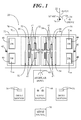
- FIG. 1 shows a top view of a MEMS device 20 in a simplified and representative form.
- MEMS device 20 may be a vibratory rate gyroscope for sensing angular velocity about an input axis.
- MEMS device 20 is referred to hereinafter as gyroscope 20.
- Gyroscope 20 is generally configured to sense angular rate about an axis of rotation referred to as an input axis 22.
- input axis 22 is the Y-axis in a three-dimensional coordinate system.
- Gyroscope 20 is illustrated as having a generally planar structure within an X-Y plane 24, wherein a Z-axis 26 extends out of the page normal to X-Y plane 24.
- Gyroscope 20 includes a first movable mass 28 and a second movable mass 30, each of which are adapted to oscillate back and forth above an underlying substrate 32 in a drive direction that is substantially parallel to an X-axis 34.
- the drive direction is orthogonal to input axis 22 of gyroscope 20.
- X-axis 34 is referred to hereinafter as drive axis 34.
- first movable mass 28 can be configured to oscillate back and forth above substrate 32.
- Second movable mass 30 can be configured to oscillate back and forth above substrate 32 in a similar manner, but one hundred eighty degrees out-of-phase with first movable mass 28, as indicated generally by the right/left set of arrows representing antiphase drive motion 38.
- the oscillatory drive motion of first and second movable masses 28, 30 may be provided in a known manner by drive electrodes 40, generally represented by rectangles and labeled DR in FIG. 1 .
- drive electrodes 40 may include sets of fixed fingers coupled to substrate 32 that are interdigitated with sets of movable fingers, where the movable fingers are coupled to and extend from first and second movable masses 28, 30.
- First and second movable masses 28, 30 may be supported above substrate 32 by various mechanical linkages 42 (e.g., drive and sense springs) that enable the out-of-phase oscillatory drive motion 36, 38 of first and second movable masses 28, 30 along drive axis 34. Further, mechanical linkages 42 enable sense motion 44 of first and second movable masses 28, 30 substantially parallel to Z-axis 26 in response to an angular input 45 (i.e., angular motion of gyroscope 20) about input axis 22. Hence, Z-axis 26 is referred to hereinafter as sense axis 26.
- a pair of sense electrodes 46, 48 can be provided on substrate 32 to detect and measure the out-of-plane deflection of first and second movable masses 28, 30.
- sense electrodes 46, 48 are obscured by the overlying movable masses 28, 30. Accordingly, in FIG. 1 , sense electrodes 46, 48 are represented in dashed line form to illustrate their physical placement relative to first and second movable masses 28, 30.
- the structural details of drive electrodes 40, mechanical linkages 42, and sense electrodes 46, 48 are not shown herein for simplicity of illustration and to avoid obscuring the exemplary and non-limiting embodiments of the invention. However, those skilled in the art will understand that drive electrodes 40, mechanical linkages 42, and sense electrodes 46, 48 can be realized in wide variety of structural configurations.
- a drive voltage, V DR can be applied to drive electrodes 40 to produce an electrostatic force between the interdigitated drive fingers that causes the drive fingers to electrostatically move with respect to one another.
- the drive voltage, V DR may be a time-varying voltage signal adapted to alternate the charge delivered to the comb fingers, which in conjunction with mechanical linkages 42, causes first and second movable masses 28, 30 to undergo oscillatory linear motion within X-Y plane 24 in antiphase.
- first and second movable masses 28, 30 are put into oscillatory drive motion 36, 38 (antiphase) along drive axis 34, the system of masses 28, 30 is capable of detecting angular input 45, i.e., angular velocity, induced by gyroscope 20 being rotated about input axis 22.
- angular input 45 i.e., angular velocity
- the Coriolis force resulting from rotational motion of gyroscope 20 about input axis 22 causes first and second movable masses 28, 30 to move out-of-plane with respect to sense electrodes 46, 48 as a function of the angular rate, i.e., angular input 45, of gyroscope 20 about input axis 22.
- This movement has an amplitude that is proportional to the angular rotation rate of gyroscope 20 about input axis 22 which can be sensed at sense electrodes 46, 48 to thereby produce a sense signal 50.
- first and second movable masses 28, 30 may undergo quadrature motion relative to sense axis 26 so that a quadrature error signal is superposed on the sense signal.
- first movable mass 28 may include at least one opening 52 extending through and fully encircled by the material structure of first movable mass 28.
- second movable mass 30 may include at least one opening 54 extending through and fully encircled by the material structure of second movable mass 30. More particularly, first movable mass 28 includes multiple openings 52 and second movable mass 30 includes multiple openings 54.
- electrodes may be vertically spaced apart from each of first and second movable masses 28, 30 proximate openings 52, 54.
- a direct current (DC) bias voltage may be applied to the electrodes to impose an electrostatic force on first and second movable masses 28, 30 to reduce or otherwise null the quadrature motion.
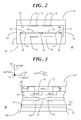
- FIG. 2 shows a side view of an integrated device 60 in a simplified and representative form.
- Integrated device 60 includes a MEMS device, e.g., gyroscope 20, and an integrated circuit (IC) die 62.
- IC die 62 may be a CMOS application specific integrated circuit (ASIC) die configured to provide the logic functions for gyroscope 20.
- ASIC application specific integrated circuit
- IC die 62 has a surface 64 coupled with gyroscope 20 via, for example, spacer element 66. Spacer element 66 may fully encircle the components of gyroscope 20 and surface 64 of IC die to form a cavity 68.
- Electrodes 70, 72 are formed on surface 64 of IC die 62 and are vertically spaced apart from a first side 74 of each of first and second movable elements 28, 30.
- Sense electrodes 46, 48 are formed on substrate 32 of gyroscope 20 and are vertically spaced apart from a second side 76 of each of first and second movable elements 28, 30, in which second side 76 opposes first side 74.
- first and second movable masses 28, 30 are interposed between substrate 32 of gyroscope 20 and surface 64 of IC die 62, and more particularly, first and second movable masses 28, 30, electrodes 70, 72, and sense electrodes 46, 48 are enclosed within the cavity 68 formed by coupling IC die 62 with gyroscope 20.
- electrodes 70, 72 may be utilized to bias movable masses 28, 30 so as to reduce quadrature motion.
- Such a configuration with electrodes 70, 72 and sense electrodes 46, 48 on opposing sides 74, 76 of first and second movable masses 28, 30, can achieve significant space savings and a reduced size relative to configurations in which electrodes 70, 72 and sense electrodes 46, 48 may be laterally disposed adjacent to one another and positioned on the same side of the movable mass(es).
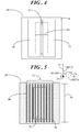
- FIG. 3 shows a partial side view of integrated device 60 and FIG. 4 shows a partial top view of gyroscope 20.
- FIG. 3 shows a portion of first movable mass 28 with a single one of openings 52 extending through it and electrodes 70, 72 being vertically spaced apart from first movable mass 28 in proximity to opening 52.
- FIG. 4 shows the same portion of first movable mass 28 as presented in FIG. 3 with one of openings 52 extending through it and electrodes 70, 72 positioned generally over opening 52.
- electrodes 70, 72 may be used for biasing first and second movable elements 28, 30 to reduce or null any possible quadrature motion of first and second movable elements 28, 30. Accordingly, electrodes 70, 72 are referred to herein as quadrature compensation electrodes 70, 72.
- Quadrature compensation electrode 70 is labeled QCU+ and quadrature compensation electrode 72 is labeled QCU- indicating that they may be differently biased, for example, opposite in polarity.
- first movable element 28 should be driven to oscillate in a manner that is substantially parallel to sense electrode 46 such that a nominal distance, D, between the oscillating mass 28 and sense electrode 46 only varies in response to changes in Coriolis force.
- manufacturing imperfections can also cause out-of-plane quadrature motion, as indicated generally by a solid arrow 78.
- This out-of-plane quadrature motion 78 can cause the nominal distance, D, between the oscillating mass 28 and sense electrode 46 to vary. Since sense signal 50 ( FIG. 1 ) is dependent upon the distance, D, any changes in distance, D, resulting from quadrature motion 78 will be injected into sense signal 50, reducing the ability of gyroscope 20 to accurately sense small changes in Coriolis force.
- a constant voltage bias V B may be applied to quadrature compensation electrode 70 while quadrature compensation electrode 72 may be kept at the same potential as first movable mass 28. As such, quadrature compensation electrode 72 would provide no interaction with first movable mass 28 in this example.
- the constant voltage bias V B will produce an electrostatic force between quadrature compensation electrode 70 and first movable mass 28 resulting in quadrature compensation motion, as indicated generally by a dashed arrow 80.
- this quadrature compensation motion 80 is approximately equal to and opposite quadrature motion 78 so as to substantially cancel quadrature motion 78.
- two metal electrodes e.g., quadrature compensation electrodes 70, 72 formed on surface 64 of IC die 62
- quadrature compensation electrodes 70, 72 formed on surface 64 of IC die 62
- a misalignment of the IC die 62 to gyroscope 20 bond could adversely affect the appropriate location of quadrature compensation electrodes 70, 72 relative to opening 52.
- a width 81 of fourteen microns for opening 52 in movable mass 28 would be required.
- the width 81 of opening 52 needs to be thirty-four microns in order to maintain normal operation. This greater width of openings 52 decreases the sense area and therefore undesirably decreases the sensitivity of gyroscope 20.
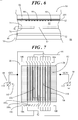
- FIG. 5 shows a partial top view of MEMS gyroscope 20 and an electrode structure 82 in accordance with an embodiment
- FIG. 6 shows a partial side view of an integrated device 84 that includes gyroscope 20 coupled with an IC die 86 in accordance with an embodiment
- IC die 86 has a surface 88 coupled with gyroscope 20 such that movable masses 28, 30 ( FIG. 1 ) are interposed between substrate 32 and surface 88 of IC die 86.
- FIGs. 5 and 6 only show a portion of first movable mass 28 with a single one of openings 52 extending through it, thus corresponding with FIGs. 3 and 4 .
- integrated device 84 includes the entire structure of gyroscope 20 described above. Further, first movable mass 28 is shown with stippling in order to better visualize opening 52 and in order to distinguish first movable mass 28 from the overlying electrode structure 82.
- Electrode structure 82 is formed on surface 88 of IC die 86.
- electrode structure 82 includes a plurality of electrode segments 90 (shown with rightwardly and downwardly directed wide hatching) vertically spaced apart from first side 74 of movable mass 28.
- sense electrode 46 is formed on substrate 32 and is vertically spaced apart from second side 76 of first movable mass 28. Accordingly, first sense mass 28, electrode structure 82 having a plurality of electrode segments 90, and sense electrode 46 are enclosed within a cavity 92 formed by coupling IC die 86 with gyroscope 20 via, for example, spacer elements (not shown).
- electrode segments 90 function as quadrature compensation electrodes in lieu of quadrature compensation electrodes 70, 72.
- electrode segments 90 may serve as sense electrodes in alternative embodiments.
- Electrode segments 90 are suitably formed on surface 88 of IC die 86 and overlie opening 52. Additionally, each of electrode segments 90 has a lengthwise dimension 94 that is oriented approximately perpendicular to the drive direction, where the drive direction is substantially parallel to drive axis 34. Further, lengthwise dimension 94 of electrode segments 90 is approximately parallel to input axis 22. Of course, in consideration of the entire structure, electrode segments 90 are suitably configured on surface 88 to overlie at least one each of openings 52, 54 ( FIG. 1 ) of each of first and second movable masses 28, 30 ( FIG. 1 ).
- FIG. 7 shows a partial top view of the gyroscope 20 and electrode structure 82, along with a switch structure 96 and control circuitry 98 simplistically represented by voltage source symbols. More particularly, FIG. 7 shows only a portion of first movable mass 28 with a single one of openings 52 extending through it, thus corresponding with FIGs. 3-6 .
- Control circuitry 98 is configured to provide a bias voltage, referred to alternatively as a quadrature compensation voltage V B 102.
- Each of electrode segments 90 can be selectively connected to control circuitry 98 via switch structure 96 in order to apply quadrature compensation voltage 102 to the selected ones of electrode segments 90.
- switch structure 96 may be suitably formed in one or more routing layers 104 (see FIG. 6 ) of IC die 86, and each of electrode segments 90 is individually interconnectable with switch structure 96 as represented by individual switches 106, 108, wherein one of the pair of switches 106, 108 can be closed to connect their associated electrode segment 90 to either a positive DC voltage source (QCU+) 110 or a negative DC voltage source (QCU-) 112.
- QCU+ positive DC voltage source
- QCU- negative DC voltage source
- electrode structure 82 on surface 88 of IC die 86 facing moveable mass 28 can be subdivided into regions, i.e., subsets of electrode segments 90 via switch structure 96. As will be discussed below, these subsets of electrode segments 90 can be connected through routing layers 104 in IC die 86 to switches 106, 108 and control circuitry 98. Control circuitry 98 can then be used to activate or deactivate regions or subsets of electrode segments 90 to achieve advantageous interactions with gyroscope by applying, for example quadrature compensation voltage 102. The design of electrode segments 90 enables subsets of electrode segments 90 to be activated by control circuitry 98 to compensate for wafer bond misalignments between IC die and gyroscope 20.
- the subsets of electrode segments 90 that are activated by control circuitry 98 may be further subdivided to enable small incremental interaction force increases or decreases by switching bias levels, e.g., the magnitude of quadrature compensation voltage 102, on certain electrode segments 90.
- a method of making integrated device 84 can entail providing a MEMS wafer having a plurality of gyroscopes 20 formed thereon and providing an CMOS wafer having a plurality of IC dies 86 formed thereon, wherein each of IC dies 86 has electrode structure 82 formed on surface 88 thereof. Further, each of IC dies 86 has routing for switch structure 96 formed in routing layers 104 of the CMOS wafer, and switches 106, 108 and control circuitry 98 are provided as part of each IC die 86.
- the CMOS wafer is coupled with the MEMS wafer to form a stacked structure that includes a plurality of integrated devices 84, as previously described. Thereafter, the stacked structure may be diced, sawn, or otherwise separated to yield integrated devices 84 utilizing conventional and upcoming wafer fabrication processes.
- FIG. 8 shows a partial top view of gyroscope 20 and electrode structure 82 subject to displacement due to bond alignment mismatch.
- a center of opening 52 is represented by a dashed line 114. If no bond alignment mismatch was present, half of electrode segments 90 would be disposed on one side of dashed line 114 and the other half of electrode segments 90 would be disposed on the opposing side of dashed line 114.
- gyroscope 20 represented by the illustrated portion of first movable mass 28
- gyroscope 20 is shifted leftwardly relative to electrode segments 90 of electrode structure 82 formed on surface 88 ( FIG. 6 ) of IC die 86 ( FIG. 6 ).
- Nominal operation of gyroscope 20 with quadrature motion compensation entails applying the bias voltage (e.g., quadrature compensation voltage 102) to those electrode segments 90 that will cross opposing edges 116, 118 (see also FIG. 7 ) of opening 52 as first movable mass 28 oscillates.
- Edge 116 is obscured by one of electrode segments 90. Hence, edge 116 it is represented by a dashed line in FIG. 8 , but is visible in FIG. 7 .
- switches 106 for a first subset, labeled 90A, of electrode segments 90 that will cross edge 116 as first movable mass 28 oscillates are closed so that a constant bias voltage (e.g., quadrature compensation voltage 102) is provided between electrode segments 90A and first movable mass 28.
- switches 108 for a second subset, labeled 90B, of electrode segments 90 that will cross edge 118 as first movable mass 28 oscillates may be closed to so as to set electrode segments 90B to the same potential as first movable mass 28. Therefore, electrode segments 90B would have no interaction with first movable mass 28.
- a suitable constant bias voltage (e.g., quadrature compensation voltage 102) may be provided between electrode segments 90B and first movable mass 28.
- electrode segments 90A would be set to the same potential as first movable mass 28 so that they would have no interaction with first movable mass 28.
- electrode segments 90A serve as positive quadrature compensation electrodes and electrode quadrature compensation segments 90B serve as negative electrodes in this example.
- various electrode segments 90 can be switched on to make either the positive quadrature compensation electrode or the negative quadrature compensation electrode.
- the configuration of switch structure 96 allows for independent control of switches 106, 108 in order to produce either the positive or the negative quadrature compensation electrode (QCU+/QCU-).
- quadrature compensation voltage 102 may be applied to a first quantity of electrode segments 90, e.g., three electrode segments 90A of electrode structure 82, where the quantity is less than the total quantity of electrode segments. Additionally, an overlap area of electrode segments 90A and electrode segments 90B overlying opening 52 changes (i.e., increases and decreases) as movable mass oscillates relative to drive axis 34. This quadrature compensation voltage 102 thus produces an electrostatic force between electrode segments 90A and movable mass 28 that can reduce or null quadrature motion of first movable mass 28.
- FIG. 9 shows a block diagram of a quadrature compensation system 120 utilizing electrode structure 82.
- quadrature compensation system 120 may include electrode structure 82 having electrode segments 90 in proximity to openings 52, 54 of movable masses 28, 30 of gyroscope 20 as discussed above. For simplicity of illustration only a portion of movable mass 28 is illustrated with electrode segments 90 overlying a single opening 52 to correspond with the illustrations of FIGs. 5-8 .
- quadrature compensation system 120 may be implemented within IC die 86 ( FIG. 6 ) to yield a compact form factor.
- Quadrature compensation system 120 additionally includes active control circuitry 98 in the form of, for example, a quadrature readout block 122 for receiving sense signal 50 output from gyroscope 20.
- Quadrature readout block 122 is in communication with an analog-to-digital converter (ADC) 124 which, in turn, is in communication with a digital controller 126.
- ADC analog-to-digital converter
- Digital controller 126 may have a memory element 128 in association therewith for storage of, by way of example, an electrode segment selection process 130 and a quadrature compensation process 132.
- electrode segment selection process 130 will be discussed in connection with FIG. 10 and one example of quadrature compensation process 132 will be discussed in connection with FIG. 11 .
- Digital controller 126 outputs digital control signals, N, 134 to a digital-to-analog converter (DAC) 136.
- DAC 136 converts digital control signals 134 to analog signals and communicates analog voltage control signals (V DC ) 138 to positive and/or negative quadrature DC voltage source(s) 110, 112. Additionally, DAC 136 may communicate analog switch control signals (SW) 140 to switch structure 96. Thereafter, quadrature control signals, e.g., a positive DC voltage (QCU+) 142 may be provided to a subset of electrode segments 90 while another subset of electrode segments 90 may be held at the same potential as movable mass 28 (represented by QCU- 144).
- QCU+ positive DC voltage
- the circuitry associated with gyroscope 20 can additionally include drive-mode circuitry 146 and sense-mode circuitry 148.
- the elements of drive-mode circuitry 146 and/or sense-mode circuitry 148 may be shared with or may be provided separately from quadrature compensation system 120.
- Each of drive-mode circuitry 146 and sense-mode circuitry 148 are simply represented by boxes in FIG. 9 and will not be described in detail herein so as to not unnecessarily obscure the features of quadrature compensation system 120.
- Quadrature readout block 122 includes a capacitance-to-voltage (C2V) unit 150 and a quadrature sampler 152.
- Capacitance-to-voltage unit 150 is connected to, for example, sense electrodes 46, 48 ( FIG. 1 ) of a sense measurement unit (not shown) and is arranged to provide a measure of the capacitance between movable masses 28, 30 and sense electrodes 46, 48 (e.g., sense signal 50) as a sense measurement voltage signal (SMV) 154.
- sense measurement voltage signal 154 is indicative of a displacement of movable masses 28, 30 along sense axis 26 (i.e., the Z-axis). Such displacement may be associated with the Coriolis force induced by an angular rotation rate about input axis 22 (i.e., the Y-axis).
- Quadrature sampler 152 may be connected to a clock sampler (not shown) to receive a digital signal as a quadrature sample clock (QCLK) 156.
- Quadrature sampler 152 is configured to receive sense measurement voltage signal 154 from capacitance-to-voltage unit 150.
- Quadrature sampler 152 is arranged to sample sense measurement voltage signal 154 with quadrature sample clock 156 to obtain analog quadrature sample values (AQV) 158.
- Analog quadrature sample values 158 can be an analog measure.
- ADC 124 is arranged to convert quadrature sense sample values 158 into a digital quadrature values (DQV) 160.
- Digital controller 126 is configured to receive digital quadrature values 160 in order to perform electrode segment selection process 130 ( FIG.
- quadrature compensation system 120 depicted herein is merely illustrative. Those skilled in the art will recognize that many other architectures may be implemented for control circuitry 98 of quadrature compensation system 120 which achieve the same functionality of providing quadrature compensation.
- FIG. 10 shows a flowchart of electrode segment selection process 130 that may be executed by digital controller 126 ( FIG. 9 ) of quadrature compensation system 120 ( FIG. 9 ). More particularly, electrode segment selection process 130 may be executed to determine which switches 106, 108 should be closed in order to select a subset of electrode segments 90 as QCU+ electrodes (e.g., electrode segments 90A) and to select another subset of electrode segments 90 as QCU- electrodes (e.g., electrode segments 90B). That is, in order to compensate for quadrature motion, the bias voltage (e.g., quadrature compensation voltage 102 of FIG.
- the bias voltage e.g., quadrature compensation voltage 102 of FIG.
- Electrode segment selection process 130 should be applied to those electrode segments 90 that will cross opposing edges 116, 118 of opening 52 as first movable mass 28 oscillates.
- Execution of electrode segment selection process 130 is not intended to remove existing quadrature motion. Rather, the objective of electrode segment selection process 130 is to find the optimal number of electrode segments 90 to be activated. Once the optimal number of electrode segments 90 is discovered, the bias voltage can be set on them such that the quadrature motion is reduced or nulled.
- the ensuing discussion refers to electrode segments 90 associated with first movable mass 28 and a single one of openings 52. It should be understood, however, the discussion applies equivalently electrode segments 90 associated with the multiple openings 52 of first movable mass 28 and to electrode segments 90 associated with multiple openings 54 of second movable mass 30 ( FIG. 1 ).
- first movable mass 28 is driven to oscillate relative to drive axis 34.
- a quadrature voltage is set to a fixed DC value. That is, positive DC voltage source 110 is set to some predetermined DC value such that there is a bias or differential to the voltage set on first movable mass 28.
- a first switch of switch structure 96 is closed while all of the remaining switches are open. Referring particularly to FIG. 7 , a first switch 106, labeled 106 1 , may be closed. Thus, the fixed DC quadrature voltage is applied to first switch 106 1 .
- a quadrature value is measured. Since an angular velocity about input axis 22 is not being imposed on gyroscope 20, the quadrature value is generally the amplitude of sense signal 50 in phase with the drive signal. The measured quadrature value is at least temporarily stored or otherwise saved at a block 170.
- the next switch of switch structure 96 is closed.
- the next switch may be associated with the electrode segment immediately adjacent to the first electrode segment 90 that was activated.
- the "next" switch 106 labeled 106 2 , may be closed.
- the current quadrature value i.e., the amplitude of sense signal 50 in phase with the drive signal
- a determination is made as to whether the current quadrature value (measured at block 176) has changed (i.e., increased or decreased) since its starting value stored at block 170. In some scenarios, "change" may be detected when the current quadrature value exceeds some threshold value relative to the stored quadrature value.
- process control loops back to block 170 to store the most recent quadrature value, to increment the electrode counter at block 172, and to thereafter close the next switch (labeled 106 3 ) in FIG. 7 .
- a block 180 concludes that the optimal number of electrode segments 90 has been discovered. This optimal number can be the quantity stored in the electrode counter at block 172. Thereafter, process 130 ends.
- Electrode segment selection process 130 is described in connection with determining the number of electrode segments 90 that may be designated as the QCU+ electrode upon which a positive DC bias voltage (e.g., quadrature compensation voltage 102 of FIG. 7 ) is to be applied in order to compensate for quadrature motion. Electrode segment selection process 130 may be repeated to determine the number of electrode segments 90 that may be designated as the QCU- electrode which are to be set to the same potential as first movable mass 28. The repeated execution of electrode segment selection process 130 may entail successively closing switches 108 to determine the number of electrode segments 90 that may be designated as the QCU- electrode. Further, additional processing may be performed to potentially "deselect" electrode segments 90 that do not contribute significantly to quadrature motion compensation. Referring briefly to the example presented in FIG. 8 , when electrode segments 90 are misaligned relative to opening 52, the rightmost electrode segments 90 may not contribute significantly to quadrature motion compensation since they would not cross edge 118. Therefore, in some embodiments, switch elements 108 associated with these electrode segments 90 may be opened.
- FIG. 11 shows a flowchart of quadrature error compensation process 132.
- Process 132 may be executed by digital controller 126 of quadrature compensation system 120 to reduce or null quadrature motion of gyroscope 20 of integrated device 84 ( FIG. 6 ).
- drive mode circuitry 146, sense mode circuitry 148, and quadrature compensation system 120 are enabled. Thereafter, at a block 184, quadrature error is extracted from sense measurement voltage signal 154 which is a voltage representative of sense signal 50. At a block 186, digital controller 126 calculates an amount of compensation that may be needed in response to receipt of digital quadrature values 160. At a block 188, the DC voltage applied to the QCU+ electrode segments 90 and the QCU- electrode segments 90 is adjusted. The DC voltage applied to the selected electrode segments 90 is configured to modulate a magnitude of an electrostatic force applied to first and second movable masses 28, 30 ( FIG. 1 ) to reduce quadrature motion of first and second movable masses 28, 30.
- quadrature error is again extracted from sense measurement voltage signal 154.
- a determination is made as to whether an optimal quadrature compensation setting has been reached. In other words, a determination is made at query block 192 that quadrature motion has been sufficiently reduced or completely nulled.
- process control loops back to block 186 to again calculate the amount of compensation needed in response to the extracted quadrature error.
- process control provides feedback control in order to converge to the optimal voltage bias applied to the selected electrode segments that gives the lowest possible level of quadrature error.
- quadrature error compensation process 132 ends.
- process 132 may be periodically repeated to ascertain that the saved quadrature compensation setting remains optimal.
- An embodiment of an integrated device comprises a microelectromechanical systems (MEMS) device having a movable mass spaced apart from a substrate, the movable mass being configured to oscillate in a drive direction relative to the substrate.
- the integrated device further comprises an integrated circuit (IC) die having a surface coupled with the MEMS device such that the movable mass is interposed between the substrate and the surface of the IC die, and an electrode structure formed on the surface of the IC die, the electrode structure including a plurality of electrode segments vertically spaced apart from the movable mass.
- MEMS microelectromechanical systems
- IC integrated circuit
- An embodiment of a method for making an integrated device comprises providing a microelectromechanical systems (MEMS) device having a movable mass spaced apart from a substrate, the movable mass being configured to oscillate in a drive direction relative to the substrate.
- the method further comprises providing an integrated circuit (IC) die having a surface, providing an electrode structure on the surface of the IC die, the electrode structure including a plurality of electrode segments, and coupling the surface of the IC die with the MEMS device such that the movable mass and the electrode structure are enclosed within a cavity formed by the coupling of the integrated circuit die with the MEMS device, and the plurality of electrode segments is vertically spaced apart from the movable mass.
- MEMS microelectromechanical systems
- An embodiment of a system comprises an integrated device comprising a microelectromechanical systems (MEMS) gyroscope having a movable mass spaced apart from a substrate, the movable mass being configured to oscillate in a drive direction relative to the substrate.
- the integrated device further comprises an integrated circuit (IC) die having a surface coupled with the MEMS device such that the movable mass is interposed between the substrate and the surface of the IC die, and an electrode structure formed on the surface of the IC die, the electrode structure including a plurality of electrode segments vertically spaced apart from the movable mass.
- MEMS microelectromechanical systems
- the system further comprises control circuitry for providing a quadrature compensation voltage, wherein each of the plurality of electrode segments is selectively connected to the control circuitry in order to apply the quadrature compensation voltage to selected ones of the electrode segments, the quadrature compensation voltage being configured to modulate a magnitude of an electrostatic force applied to the movable element to reduce quadrature motion of the movable mass.
- embodiments entail an integrated device that includes a MEMS device vertically bonded with an IC die, such as a CMOS die, and fabrication methodology for producing the integrated device.
- An electrode structure is formed on a surface of the IC die facing a movable mass of the MEMS device, for example, a MEMS gyroscope.
- the electrode structure includes a plurality of electrode segments that are connected through routing layers on the CMOS die to a switch structure and an active circuit.
- the active circuit can be used to selectively activate or deactivate particular electrode segments to achieve advantageous interaction with the movable mass of the MEMS device. That is, the electrode segments can be used to apply electrostatic forces to the movable mass of the MEMS device in order to compensate for quadrature motion.
- particular electrode segments can be activated in order to compensate for bonding misalignments between the IC die and the MEMS device. Still further, the electrode segments may be selectively activated in order to allow incremental electrostatic force increases or decreases by switching voltage bias levels on the electrode segments via the active circuit.
Landscapes
- Engineering & Computer Science (AREA)
- Manufacturing & Machinery (AREA)
- Physics & Mathematics (AREA)
- General Physics & Mathematics (AREA)
- Radar, Positioning & Navigation (AREA)
- Remote Sensing (AREA)
- Microelectronics & Electronic Packaging (AREA)
- Signal Processing (AREA)
- Gyroscopes (AREA)
Abstract
Description
- The present invention relates generally to the field of microelectromechanical systems (MEMS). More specifically, the present invention relates to a segmented electrode structure for quadrature reduction in a MEMS-CMOS integrated device.
- Microelectromechanical systems (MEMS) technology has achieved wide popularity in recent years, as it provides a way to make very small mechanical structures and integrate these structures with electrical devices on a single substrate using conventional batch semiconductor processing techniques. One common application of MEMS is the design and manufacture of sensor devices. MEMS sensors are widely used in applications such as automotive, inertial guidance systems, household appliances, game devices, protection systems for a variety of devices, and many other industrial, scientific, and engineering systems. One example of a MEMS sensor is a MEMS angular rate sensor. Alternatively referred to as a "gyroscope", "vibratory angular rate sensors," "vibratory rate gyroscopes," "gyroscope sensor," or "yaw rate sensor," an angular rate sensor senses angular speed or velocity around one or more axes.
- In vibratory angular rate sensors, an inherent problem is the existence of undesirable interference signals, referred to as a quadrature component or quadrature error. Quadrature error is due to quadrature motion, for example, motion out-of-plane of the proof mass as it oscillates back and forth above the sense electrode. Quadrature motion can occur in vibrating angular rate sensors due to manufacturing imperfections. When present, quadrature motion creates an oscillation on the sense axis that can be confused with Coriolis acceleration and subsequently, the rotation rate. Unfortunately, quadrature error can result in offset error, reduced dynamic range, and increased noise for the device. A large quadrature error can even cause a device to rail so that the sense mass comes into contact with conductive electrodes potentially resulting in collision-related damage, such as a short.
- The accompanying figures in which like reference numerals refer to identical or functionally similar elements throughout the separate views, the figures are not necessarily drawn to scale, and which together with the detailed description below are incorporated in and form part of the specification, serve to further illustrate various embodiments and to explain various principles and advantages all in accordance with the present invention.
-
FIG. 1 shows a top view of a microelectromechanical systems (MEMS) gyroscope in a simplified and representative form; -
FIG. 2 shows a side view of an integrated device in a simplified and representative form; -
FIG. 3 shows a partial side view of the integrated device ofFIG. 2 ; -
FIG. 4 shows a partial top view of a MEMS gyroscope; -
FIG. 5 shows a partial top view of the MEMS gyroscope ofFIG. 1 in accordance with an embodiment; -
FIG. 6 shows a partial side view of an integrated device that includes the MEMS gyroscope ofFIG. 1 and an electrode structure; -
FIG. 7 shows a partial top view of the MEMS gyroscope and the electrode structure ofFIG. 6 along with a switch structure and associated control circuitry; -
FIG. 8 shows a partial top view of the MEMS gyroscope and the electrode structure subject to displacement due to bond alignment mismatch; -
FIG. 9 shows a block diagram of a quadrature compensation system utilizing the electrode structure; -
FIG. 10 shows a flowchart of an electrode segment selection process; and -
FIG. 11 shows a flowchart of a quadrature error compensation process. - Embodiments disclosed herein include an integrated device that includes a microelectromechanical systems (MEMS) device vertically bonded with an integrated circuit (IC) die, such as a complimentary metal-oxide-semiconductor (CMOS) die, and fabrication methodology for producing the integrated device. An electrode structure is formed on a surface of the IC die facing a movable mass of the MEMS device, for example, a MEMS gyroscope. The electrode structure includes a plurality of electrode segments that are connected through routing layers on the CMOS die to a switch structure and an active circuit. The active circuit can be used to selectively activate or deactivate particular electrode segments to achieve advantageous interaction with the movable mass of the MEMS device. That is, the electrode segments can be used to apply electrostatic forces to the movable mass of the MEMS device in order to compensate for quadrature motion. Further, particular electrode segments can be activated in order to compensate for bonding misalignments between the IC die and the MEMS device. Still further, the electrode segments may be selectively activated in order to allow incremental electrostatic force increases or decreases by switching voltage bias levels on the electrode segments via the active circuit.
- The instant disclosure is provided to further explain in an enabling fashion the best modes, at the time of the application, of making and using various embodiments in accordance with the present invention. The disclosure is further offered to enhance an understanding and appreciation for the inventive principles and advantages thereof, rather than to limit in any manner the invention. The invention is defined solely by the appended claims including any amendments made during the pendency of this application and all equivalents of those claims as issued.
- It should be understood that the use of relational terms, if any, such as first and second, top and bottom, and the like may be used herein solely to distinguish one from another entity or action without necessarily requiring or implying any actual such relationship or order between such entities or actions. Furthermore, some of the figures may be illustrated using various shading and/or hatching to distinguish the different elements produced within the various structural layers. These different elements within the structural layers may be produced utilizing current and upcoming microfabrication techniques of depositing, patterning, etching, and so forth. Accordingly, although different shading and/or hatching is utilized in the illustrations, the different elements within the structural layers may be formed out of the same material.
- Referring to
FIG. 1, FIG. 1 shows a top view of aMEMS device 20 in a simplified and representative form.MEMS device 20 may be a vibratory rate gyroscope for sensing angular velocity about an input axis. Thus,MEMS device 20 is referred to hereinafter asgyroscope 20. Gyroscope 20 is generally configured to sense angular rate about an axis of rotation referred to as aninput axis 22. In the illustrated configuration,input axis 22 is the Y-axis in a three-dimensional coordinate system. Gyroscope 20 is illustrated as having a generally planar structure within anX-Y plane 24, wherein a Z-axis 26 extends out of the page normal toX-Y plane 24. -
Gyroscope 20 includes a firstmovable mass 28 and a secondmovable mass 30, each of which are adapted to oscillate back and forth above anunderlying substrate 32 in a drive direction that is substantially parallel to anX-axis 34. Thus, the drive direction is orthogonal to inputaxis 22 ofgyroscope 20. Accordingly,X-axis 34 is referred to hereinafter asdrive axis 34. As indicated by the left/right set of arrows representingdrive motion 36, firstmovable mass 28 can be configured to oscillate back and forth abovesubstrate 32. Secondmovable mass 30 can be configured to oscillate back and forth abovesubstrate 32 in a similar manner, but one hundred eighty degrees out-of-phase with firstmovable mass 28, as indicated generally by the right/left set of arrows representingantiphase drive motion 38. The oscillatory drive motion of first and secondmovable masses drive electrodes 40, generally represented by rectangles and labeled DR inFIG. 1 . Although not shown in detail,drive electrodes 40 may include sets of fixed fingers coupled tosubstrate 32 that are interdigitated with sets of movable fingers, where the movable fingers are coupled to and extend from first and secondmovable masses - First and second
movable masses substrate 32 by various mechanical linkages 42 (e.g., drive and sense springs) that enable the out-of-phaseoscillatory drive motion movable masses drive axis 34. Further,mechanical linkages 42 enablesense motion 44 of first and secondmovable masses axis 26 in response to an angular input 45 (i.e., angular motion of gyroscope 20) aboutinput axis 22. Hence, Z-axis 26 is referred to hereinafter assense axis 26. A pair ofsense electrodes substrate 32 to detect and measure the out-of-plane deflection of first and secondmovable masses FIG. 1 ,sense electrodes movable masses FIG. 1 ,sense electrodes movable masses drive electrodes 40,mechanical linkages 42, andsense electrodes electrodes 40,mechanical linkages 42, andsense electrodes - In operation, a drive voltage, VDR, can be applied to drive
electrodes 40 to produce an electrostatic force between the interdigitated drive fingers that causes the drive fingers to electrostatically move with respect to one another. The drive voltage, VDR, may be a time-varying voltage signal adapted to alternate the charge delivered to the comb fingers, which in conjunction withmechanical linkages 42, causes first and secondmovable masses X-Y plane 24 in antiphase. Once first and secondmovable masses oscillatory drive motion 36, 38 (antiphase) alongdrive axis 34, the system ofmasses angular input 45, i.e., angular velocity, induced bygyroscope 20 being rotated aboutinput axis 22. In particular, the Coriolis force resulting from rotational motion ofgyroscope 20 aboutinput axis 22 causes first and secondmovable masses sense electrodes angular input 45, ofgyroscope 20 aboutinput axis 22. This movement has an amplitude that is proportional to the angular rotation rate ofgyroscope 20 aboutinput axis 22 which can be sensed atsense electrodes sense signal 50. - As mentioned previously, manufacturing imperfections in
gyroscope 20 may permit first and secondmovable masses axis 26 so that a quadrature error signal is superposed on the sense signal. In one structural configuration, firstmovable mass 28 may include at least oneopening 52 extending through and fully encircled by the material structure of firstmovable mass 28. Likewise, secondmovable mass 30 may include at least oneopening 54 extending through and fully encircled by the material structure of secondmovable mass 30. More particularly, firstmovable mass 28 includesmultiple openings 52 and secondmovable mass 30 includesmultiple openings 54. As will be discussed in significantly greater detail below, electrodes may be vertically spaced apart from each of first and secondmovable masses proximate openings movable masses -
FIG. 2 shows a side view of anintegrated device 60 in a simplified and representative form.Integrated device 60 includes a MEMS device, e.g.,gyroscope 20, and an integrated circuit (IC) die 62. In this example, IC die 62 may be a CMOS application specific integrated circuit (ASIC) die configured to provide the logic functions forgyroscope 20. IC die 62 has asurface 64 coupled withgyroscope 20 via, for example,spacer element 66.Spacer element 66 may fully encircle the components ofgyroscope 20 andsurface 64 of IC die to form acavity 68.Electrodes surface 64 of IC die 62 and are vertically spaced apart from afirst side 74 of each of first and secondmovable elements Sense electrodes substrate 32 ofgyroscope 20 and are vertically spaced apart from asecond side 76 of each of first and secondmovable elements second side 76 opposesfirst side 74. - Thus, first and second
movable masses substrate 32 ofgyroscope 20 andsurface 64 of IC die 62, and more particularly, first and secondmovable masses electrodes sense electrodes cavity 68 formed by coupling IC die 62 withgyroscope 20. In this theoretical configuration,electrodes movable masses electrodes sense electrodes sides movable masses electrodes sense electrodes - Referring now to
FIGs. 3 and4 in connection withFIG. 2, FIG. 3 shows a partial side view ofintegrated device 60 andFIG. 4 shows a partial top view ofgyroscope 20. By way of example,FIG. 3 shows a portion of firstmovable mass 28 with a single one ofopenings 52 extending through it andelectrodes movable mass 28 in proximity to opening 52. Likewise,FIG. 4 shows the same portion of firstmovable mass 28 as presented inFIG. 3 with one ofopenings 52 extending through it andelectrodes opening 52. In this example,electrodes movable elements movable elements electrodes quadrature compensation electrodes Quadrature compensation electrode 70 is labeled QCU+ andquadrature compensation electrode 72 is labeled QCU- indicating that they may be differently biased, for example, opposite in polarity. - Ideally, first
movable element 28 should be driven to oscillate in a manner that is substantially parallel tosense electrode 46 such that a nominal distance, D, between theoscillating mass 28 andsense electrode 46 only varies in response to changes in Coriolis force. However, manufacturing imperfections can also cause out-of-plane quadrature motion, as indicated generally by asolid arrow 78. This out-of-plane quadrature motion 78 can cause the nominal distance, D, between theoscillating mass 28 andsense electrode 46 to vary. Since sense signal 50 (FIG. 1 ) is dependent upon the distance, D, any changes in distance, D, resulting fromquadrature motion 78 will be injected intosense signal 50, reducing the ability ofgyroscope 20 to accurately sense small changes in Coriolis force. - To counterbalance
quadrature motion 78, a constant voltage bias VB may be applied toquadrature compensation electrode 70 whilequadrature compensation electrode 72 may be kept at the same potential as firstmovable mass 28. As such,quadrature compensation electrode 72 would provide no interaction with firstmovable mass 28 in this example. The constant voltage bias VB will produce an electrostatic force betweenquadrature compensation electrode 70 and firstmovable mass 28 resulting in quadrature compensation motion, as indicated generally by a dashedarrow 80. In this example, asmovable mass 28 moves rightwardly, the overlap area withquadrature compensation electrode 70 will increase therefore increasing the vertical electrostatic force. Asmovable mass 28 moves leftwardly, the overlap area withquadrature compensation electrode 72 will decrease therefore decreasing the vertical electrostatic force. Ideally, thisquadrature compensation motion 80 is approximately equal to andopposite quadrature motion 78 so as to substantially cancelquadrature motion 78. - In this theoretical configuration, two metal electrodes (e.g.,
quadrature compensation electrodes surface 64 of IC die 62) are arranged to overlie opening 52 extending through firstmovable mass 28. When IC die 62 is subsequently bonded togyroscope 20, a misalignment of the IC die 62 to gyroscope 20 bond could adversely affect the appropriate location ofquadrature compensation electrodes opening 52. In order to enable nominal operation in this theoretical configuration when there is no bond misalignment and with, for example, drive motion of +/- five microns, awidth 81 of fourteen microns for opening 52 inmovable mass 28 would be required. Some specifications allow +/ten microns of bond misalignment. Accordingly, for +/- ten microns of bond misalignment, thewidth 81 of opening 52 needs to be thirty-four microns in order to maintain normal operation. This greater width ofopenings 52 decreases the sense area and therefore undesirably decreases the sensitivity ofgyroscope 20. - Referring now to
FIGs. 5 and6 ,FIG. 5 shows a partial top view ofMEMS gyroscope 20 and anelectrode structure 82 in accordance with an embodiment andFIG. 6 shows a partial side view of anintegrated device 84 that includesgyroscope 20 coupled with an IC die 86 in accordance with an embodiment. Like the previous illustrations, IC die 86 has asurface 88 coupled withgyroscope 20 such thatmovable masses 28, 30 (FIG. 1 ) are interposed betweensubstrate 32 andsurface 88 of IC die 86. In this simplified illustration,FIGs. 5 and6 only show a portion of firstmovable mass 28 with a single one ofopenings 52 extending through it, thus corresponding withFIGs. 3 and4 . However, it should be understood that the ensuing discussion applies equally to a structural configuration in which integrateddevice 84 includes the entire structure ofgyroscope 20 described above. Further, firstmovable mass 28 is shown with stippling in order to better visualize opening 52 and in order to distinguish firstmovable mass 28 from the overlyingelectrode structure 82. -
Electrode structure 82 is formed onsurface 88 of IC die 86. In accordance with a particular embodiment,electrode structure 82 includes a plurality of electrode segments 90 (shown with rightwardly and downwardly directed wide hatching) vertically spaced apart fromfirst side 74 ofmovable mass 28. Again,sense electrode 46 is formed onsubstrate 32 and is vertically spaced apart fromsecond side 76 of firstmovable mass 28. Accordingly,first sense mass 28,electrode structure 82 having a plurality ofelectrode segments 90, andsense electrode 46 are enclosed within acavity 92 formed by coupling IC die 86 withgyroscope 20 via, for example, spacer elements (not shown). Again, such a configuration can achieve significant space savings and a reduced size relative to configurations in which all electrodes (i.e., both sense and quadrature compensation electrodes) may be laterally disposed adjacent to one another and positioned on the same side of the movable mass(es). In a non-limiting embodiment,electrode segments 90 function as quadrature compensation electrodes in lieu ofquadrature compensation electrodes electrode segments 90 may serve as sense electrodes in alternative embodiments. -
Electrode segments 90 are suitably formed onsurface 88 of IC die 86 and overlieopening 52. Additionally, each ofelectrode segments 90 has alengthwise dimension 94 that is oriented approximately perpendicular to the drive direction, where the drive direction is substantially parallel to driveaxis 34. Further,lengthwise dimension 94 ofelectrode segments 90 is approximately parallel to inputaxis 22. Of course, in consideration of the entire structure,electrode segments 90 are suitably configured onsurface 88 to overlie at least one each ofopenings 52, 54 (FIG. 1 ) of each of first and secondmovable masses 28, 30 (FIG. 1 ). - With reference now to
FIGs. 5 ,6, and 7, FIG. 7 shows a partial top view of thegyroscope 20 andelectrode structure 82, along with aswitch structure 96 andcontrol circuitry 98 simplistically represented by voltage source symbols. More particularly,FIG. 7 shows only a portion of firstmovable mass 28 with a single one ofopenings 52 extending through it, thus corresponding withFIGs. 3-6 .Control circuitry 98 is configured to provide a bias voltage, referred to alternatively as a quadraturecompensation voltage V B 102. Each ofelectrode segments 90 can be selectively connected to controlcircuitry 98 viaswitch structure 96 in order to applyquadrature compensation voltage 102 to the selected ones ofelectrode segments 90. - The electrical interconnects and switches of
switch structure 96 may be suitably formed in one or more routing layers 104 (seeFIG. 6 ) of IC die 86, and each ofelectrode segments 90 is individually interconnectable withswitch structure 96 as represented byindividual switches switches electrode segment 90 to either a positive DC voltage source (QCU+) 110 or a negative DC voltage source (QCU-) 112. Thus, switchstructure 96 enables selective connection ofindividual electrode segments 90 to controlcircuitry 98. - The design of
electrode structure 82 onsurface 88 of IC die 86 facingmoveable mass 28 can be subdivided into regions, i.e., subsets ofelectrode segments 90 viaswitch structure 96. As will be discussed below, these subsets ofelectrode segments 90 can be connected through routinglayers 104 in IC die 86 toswitches control circuitry 98.Control circuitry 98 can then be used to activate or deactivate regions or subsets ofelectrode segments 90 to achieve advantageous interactions with gyroscope by applying, for examplequadrature compensation voltage 102. The design ofelectrode segments 90 enables subsets ofelectrode segments 90 to be activated bycontrol circuitry 98 to compensate for wafer bond misalignments between IC die andgyroscope 20. Alternatively, or additionally, the subsets ofelectrode segments 90 that are activated bycontrol circuitry 98 may be further subdivided to enable small incremental interaction force increases or decreases by switching bias levels, e.g., the magnitude ofquadrature compensation voltage 102, oncertain electrode segments 90. - A method of making
integrated device 84 can entail providing a MEMS wafer having a plurality ofgyroscopes 20 formed thereon and providing an CMOS wafer having a plurality of IC dies 86 formed thereon, wherein each of IC dies 86 haselectrode structure 82 formed onsurface 88 thereof. Further, each of IC dies 86 has routing forswitch structure 96 formed in routinglayers 104 of the CMOS wafer, and switches 106, 108 andcontrol circuitry 98 are provided as part of each IC die 86. The CMOS wafer is coupled with the MEMS wafer to form a stacked structure that includes a plurality ofintegrated devices 84, as previously described. Thereafter, the stacked structure may be diced, sawn, or otherwise separated to yieldintegrated devices 84 utilizing conventional and upcoming wafer fabrication processes. -
FIG. 8 shows a partial top view ofgyroscope 20 andelectrode structure 82 subject to displacement due to bond alignment mismatch. A center of opening 52 is represented by a dashedline 114. If no bond alignment mismatch was present, half ofelectrode segments 90 would be disposed on one side of dashedline 114 and the other half ofelectrode segments 90 would be disposed on the opposing side of dashedline 114. In this example, whenmovable mass 28 is not subjected to oscillatory drive motion, gyroscope 20 (represented by the illustrated portion of first movable mass 28) is shifted leftwardly relative toelectrode segments 90 ofelectrode structure 82 formed on surface 88 (FIG. 6 ) of IC die 86 (FIG. 6 ). - Nominal operation of
gyroscope 20 with quadrature motion compensation entails applying the bias voltage (e.g., quadrature compensation voltage 102) to those electrodesegments 90 that will cross opposingedges 116, 118 (see alsoFIG. 7 ) of opening 52 as firstmovable mass 28 oscillates.Edge 116 is obscured by one ofelectrode segments 90. Hence,edge 116 it is represented by a dashed line inFIG. 8 , but is visible inFIG. 7 . Accordingly, in this example, switches 106 for a first subset, labeled 90A, ofelectrode segments 90 that will crossedge 116 as firstmovable mass 28 oscillates are closed so that a constant bias voltage (e.g., quadrature compensation voltage 102) is provided betweenelectrode segments 90A and firstmovable mass 28. Conversely, switches 108 for a second subset, labeled 90B, ofelectrode segments 90 that will crossedge 118 as firstmovable mass 28 oscillates may be closed to so as to setelectrode segments 90B to the same potential as firstmovable mass 28. Therefore,electrode segments 90B would have no interaction with firstmovable mass 28. In another embodiment, a suitable constant bias voltage (e.g., quadrature compensation voltage 102) may be provided betweenelectrode segments 90B and firstmovable mass 28. As such,electrode segments 90A would be set to the same potential as firstmovable mass 28 so that they would have no interaction with firstmovable mass 28. - Thus,
electrode segments 90A serve as positive quadrature compensation electrodes and electrodequadrature compensation segments 90B serve as negative electrodes in this example. Depending upon where the bond alignment (or misalignment) takes place,various electrode segments 90 can be switched on to make either the positive quadrature compensation electrode or the negative quadrature compensation electrode. The configuration ofswitch structure 96 allows for independent control ofswitches - Accordingly,
quadrature compensation voltage 102 may be applied to a first quantity ofelectrode segments 90, e.g., threeelectrode segments 90A ofelectrode structure 82, where the quantity is less than the total quantity of electrode segments. Additionally, an overlap area ofelectrode segments 90A andelectrode segments 90B overlying opening 52 changes (i.e., increases and decreases) as movable mass oscillates relative to driveaxis 34. Thisquadrature compensation voltage 102 thus produces an electrostatic force betweenelectrode segments 90A andmovable mass 28 that can reduce or null quadrature motion of firstmovable mass 28. - An example process for determining which
electrode segments 90 might be selected for quadrature motion compensation will be discussed in connection withFIG. 10 . Additionally, an example quadrature error compensation process implementing electrode structure will be discussed in connection withFIG. 11 . - Referring to
FIGs. 1 ,7 and9, FIG. 9 shows a block diagram of aquadrature compensation system 120 utilizingelectrode structure 82. More particularly,quadrature compensation system 120 may includeelectrode structure 82 havingelectrode segments 90 in proximity toopenings movable masses gyroscope 20 as discussed above. For simplicity of illustration only a portion ofmovable mass 28 is illustrated withelectrode segments 90 overlying asingle opening 52 to correspond with the illustrations ofFIGs. 5-8 . In one example,quadrature compensation system 120 may be implemented within IC die 86 (FIG. 6 ) to yield a compact form factor. -
Quadrature compensation system 120 additionally includesactive control circuitry 98 in the form of, for example, aquadrature readout block 122 for receivingsense signal 50 output fromgyroscope 20.Quadrature readout block 122 is in communication with an analog-to-digital converter (ADC) 124 which, in turn, is in communication with adigital controller 126.Digital controller 126 may have amemory element 128 in association therewith for storage of, by way of example, an electrodesegment selection process 130 and aquadrature compensation process 132. One example of electrodesegment selection process 130 will be discussed in connection withFIG. 10 and one example ofquadrature compensation process 132 will be discussed in connection withFIG. 11 .Digital controller 126 outputs digital control signals, N, 134 to a digital-to-analog converter (DAC) 136.DAC 136 converts digital control signals 134 to analog signals and communicates analog voltage control signals (VDC) 138 to positive and/or negative quadrature DC voltage source(s) 110, 112. Additionally,DAC 136 may communicate analog switch control signals (SW) 140 to switchstructure 96. Thereafter, quadrature control signals, e.g., a positive DC voltage (QCU+) 142 may be provided to a subset ofelectrode segments 90 while another subset ofelectrode segments 90 may be held at the same potential as movable mass 28 (represented by QCU- 144). - Those skilled in the art will recognize that the circuitry associated with
gyroscope 20 can additionally include drive-mode circuitry 146 and sense-mode circuitry 148. The elements of drive-mode circuitry 146 and/or sense-mode circuitry 148 may be shared with or may be provided separately fromquadrature compensation system 120. Each of drive-mode circuitry 146 and sense-mode circuitry 148 are simply represented by boxes inFIG. 9 and will not be described in detail herein so as to not unnecessarily obscure the features ofquadrature compensation system 120. -
Quadrature readout block 122 includes a capacitance-to-voltage (C2V)unit 150 and aquadrature sampler 152. Capacitance-to-voltage unit 150 is connected to, for example,sense electrodes 46, 48 (FIG. 1 ) of a sense measurement unit (not shown) and is arranged to provide a measure of the capacitance betweenmovable masses sense electrodes 46, 48 (e.g., sense signal 50) as a sense measurement voltage signal (SMV) 154. In this example, sensemeasurement voltage signal 154 is indicative of a displacement ofmovable masses -
Quadrature sampler 152 may be connected to a clock sampler (not shown) to receive a digital signal as a quadrature sample clock (QCLK) 156.Quadrature sampler 152 is configured to receive sensemeasurement voltage signal 154 from capacitance-to-voltage unit 150.Quadrature sampler 152 is arranged to sample sensemeasurement voltage signal 154 withquadrature sample clock 156 to obtain analog quadrature sample values (AQV) 158. Analog quadrature sample values 158 can be an analog measure. As such,ADC 124 is arranged to convert quadrature sense sample values 158 into a digital quadrature values (DQV) 160.Digital controller 126 is configured to receive digital quadrature values 160 in order to perform electrode segment selection process 130 (FIG. 10 ) and or quadrature compensation process 132 (FIG. 11 ) and provide, for example, control signals 134. The architecture ofquadrature compensation system 120 depicted herein is merely illustrative. Those skilled in the art will recognize that many other architectures may be implemented forcontrol circuitry 98 ofquadrature compensation system 120 which achieve the same functionality of providing quadrature compensation. - Referring to
FIGs. 1 ,7 , and10, FIG. 10 shows a flowchart of electrodesegment selection process 130 that may be executed by digital controller 126 (FIG. 9 ) of quadrature compensation system 120 (FIG. 9 ). More particularly, electrodesegment selection process 130 may be executed to determine which switches 106, 108 should be closed in order to select a subset ofelectrode segments 90 as QCU+ electrodes (e.g.,electrode segments 90A) and to select another subset ofelectrode segments 90 as QCU- electrodes (e.g.,electrode segments 90B). That is, in order to compensate for quadrature motion, the bias voltage (e.g.,quadrature compensation voltage 102 ofFIG. 7 ) should be applied to those electrodesegments 90 that will cross opposingedges movable mass 28 oscillates. Execution of electrodesegment selection process 130 is not intended to remove existing quadrature motion. Rather, the objective of electrodesegment selection process 130 is to find the optimal number ofelectrode segments 90 to be activated. Once the optimal number ofelectrode segments 90 is discovered, the bias voltage can be set on them such that the quadrature motion is reduced or nulled. Again, the ensuing discussion refers toelectrode segments 90 associated with firstmovable mass 28 and a single one ofopenings 52. It should be understood, however, the discussion appliesequivalently electrode segments 90 associated with themultiple openings 52 of firstmovable mass 28 and to electrodesegments 90 associated withmultiple openings 54 of second movable mass 30 (FIG. 1 ). - At a
block 162 of electrodesegment selection process 130, firstmovable mass 28 is driven to oscillate relative to driveaxis 34. At ablock 164, a quadrature voltage is set to a fixed DC value. That is, positiveDC voltage source 110 is set to some predetermined DC value such that there is a bias or differential to the voltage set on firstmovable mass 28. At ablock 166, a first switch ofswitch structure 96 is closed while all of the remaining switches are open. Referring particularly toFIG. 7 , afirst switch 106, labeled 1061, may be closed. Thus, the fixed DC quadrature voltage is applied tofirst switch 1061. - Next at a
block 168, a quadrature value is measured. Since an angular velocity aboutinput axis 22 is not being imposed ongyroscope 20, the quadrature value is generally the amplitude ofsense signal 50 in phase with the drive signal. The measured quadrature value is at least temporarily stored or otherwise saved at ablock 170. At ablock 172, an electrode segment counter may by incremented, E=E+1, in order to maintain a count of the selectedelectrode segments 90. Of course, during a first iteration of electrodesegment selection process 130 the total number ofelectrode segments 90 counted by the electrode segment counter will be E=1. - At a
block 174, the next switch ofswitch structure 96 is closed. The next switch may be associated with the electrode segment immediately adjacent to thefirst electrode segment 90 that was activated. Referring particularly toFIG. 7 , the "next"switch 106, labeled 1062, may be closed. At ablock 176, the current quadrature value (i.e., the amplitude ofsense signal 50 in phase with the drive signal) is measured. At aquery block 178, a determination is made as to whether the current quadrature value (measured at block 176) has changed (i.e., increased or decreased) since its starting value stored atblock 170. In some scenarios, "change" may be detected when the current quadrature value exceeds some threshold value relative to the stored quadrature value. If the current quadrature value changes relative to the stored quadrature value, process control loops back to block 170 to store the most recent quadrature value, to increment the electrode counter atblock 172, and to thereafter close the next switch (labeled 1063) inFIG. 7 . Conversely, if the current quadrature value has not changed significantly from the previously stored quadrature value, ablock 180 concludes that the optimal number ofelectrode segments 90 has been discovered. This optimal number can be the quantity stored in the electrode counter atblock 172. Thereafter,process 130 ends. - Electrode
segment selection process 130 is described in connection with determining the number ofelectrode segments 90 that may be designated as the QCU+ electrode upon which a positive DC bias voltage (e.g.,quadrature compensation voltage 102 ofFIG. 7 ) is to be applied in order to compensate for quadrature motion. Electrodesegment selection process 130 may be repeated to determine the number ofelectrode segments 90 that may be designated as the QCU- electrode which are to be set to the same potential as firstmovable mass 28. The repeated execution of electrodesegment selection process 130 may entail successively closingswitches 108 to determine the number ofelectrode segments 90 that may be designated as the QCU- electrode. Further, additional processing may be performed to potentially "deselect"electrode segments 90 that do not contribute significantly to quadrature motion compensation. Referring briefly to the example presented inFIG. 8 , whenelectrode segments 90 are misaligned relative to opening 52, therightmost electrode segments 90 may not contribute significantly to quadrature motion compensation since they would not crossedge 118. Therefore, in some embodiments, switchelements 108 associated with theseelectrode segments 90 may be opened. - Referring now to
FIGs. 9 and11, FIG. 11 shows a flowchart of quadratureerror compensation process 132.Process 132 may be executed bydigital controller 126 ofquadrature compensation system 120 to reduce or null quadrature motion ofgyroscope 20 of integrated device 84 (FIG. 6 ). - At a
block 182,drive mode circuitry 146,sense mode circuitry 148, andquadrature compensation system 120 are enabled. Thereafter, at ablock 184, quadrature error is extracted from sensemeasurement voltage signal 154 which is a voltage representative ofsense signal 50. At ablock 186,digital controller 126 calculates an amount of compensation that may be needed in response to receipt of digital quadrature values 160. At ablock 188, the DC voltage applied to theQCU+ electrode segments 90 and the QCU-electrode segments 90 is adjusted. The DC voltage applied to the selectedelectrode segments 90 is configured to modulate a magnitude of an electrostatic force applied to first and secondmovable masses 28, 30 (FIG. 1 ) to reduce quadrature motion of first and secondmovable masses - At a
block 190, quadrature error is again extracted from sensemeasurement voltage signal 154. At aquery block 192, a determination is made as to whether an optimal quadrature compensation setting has been reached. In other words, a determination is made atquery block 192 that quadrature motion has been sufficiently reduced or completely nulled. When an optimal quadrature compensation setting has not been reached, process control loops back to block 186 to again calculate the amount of compensation needed in response to the extracted quadrature error. Thus, process control provides feedback control in order to converge to the optimal voltage bias applied to the selected electrode segments that gives the lowest possible level of quadrature error. When a determination is made atquery block 192 that quadrature motion has been sufficiently reduced or completely nulled, the optimal quadrature compensation setting (DC bias voltage) is saved and utilized for quadrature compensation. Thereafter, quadratureerror compensation process 132 ends. Of course, in some configurations,process 132 may be periodically repeated to ascertain that the saved quadrature compensation setting remains optimal. - It is to be understood that certain ones of the process blocks depicted in
FIGs. 10-11 may be performed in parallel with each other or with performing other processes. In addition, it is to be understood that the particular ordering of the process blocks depicted inFigs. 10-11 may be modified, while achieving substantially the same result. Accordingly, such modifications are intended to be included within the scope of the inventive subject matter. - Thus, an integrated device and methodology for fabricating the integrated device have been described. An embodiment of an integrated device comprises a microelectromechanical systems (MEMS) device having a movable mass spaced apart from a substrate, the movable mass being configured to oscillate in a drive direction relative to the substrate. The integrated device further comprises an integrated circuit (IC) die having a surface coupled with the MEMS device such that the movable mass is interposed between the substrate and the surface of the IC die, and an electrode structure formed on the surface of the IC die, the electrode structure including a plurality of electrode segments vertically spaced apart from the movable mass.
- An embodiment of a method for making an integrated device comprises providing a microelectromechanical systems (MEMS) device having a movable mass spaced apart from a substrate, the movable mass being configured to oscillate in a drive direction relative to the substrate. The method further comprises providing an integrated circuit (IC) die having a surface, providing an electrode structure on the surface of the IC die, the electrode structure including a plurality of electrode segments, and coupling the surface of the IC die with the MEMS device such that the movable mass and the electrode structure are enclosed within a cavity formed by the coupling of the integrated circuit die with the MEMS device, and the plurality of electrode segments is vertically spaced apart from the movable mass.
- An embodiment of a system comprises an integrated device comprising a microelectromechanical systems (MEMS) gyroscope having a movable mass spaced apart from a substrate, the movable mass being configured to oscillate in a drive direction relative to the substrate. The integrated device further comprises an integrated circuit (IC) die having a surface coupled with the MEMS device such that the movable mass is interposed between the substrate and the surface of the IC die, and an electrode structure formed on the surface of the IC die, the electrode structure including a plurality of electrode segments vertically spaced apart from the movable mass. The system further comprises control circuitry for providing a quadrature compensation voltage, wherein each of the plurality of electrode segments is selectively connected to the control circuitry in order to apply the quadrature compensation voltage to selected ones of the electrode segments, the quadrature compensation voltage being configured to modulate a magnitude of an electrostatic force applied to the movable element to reduce quadrature motion of the movable mass.
- Accordingly, embodiments entail an integrated device that includes a MEMS device vertically bonded with an IC die, such as a CMOS die, and fabrication methodology for producing the integrated device. An electrode structure is formed on a surface of the IC die facing a movable mass of the MEMS device, for example, a MEMS gyroscope. The electrode structure includes a plurality of electrode segments that are connected through routing layers on the CMOS die to a switch structure and an active circuit. The active circuit can be used to selectively activate or deactivate particular electrode segments to achieve advantageous interaction with the movable mass of the MEMS device. That is, the electrode segments can be used to apply electrostatic forces to the movable mass of the MEMS device in order to compensate for quadrature motion. Further, particular electrode segments can be activated in order to compensate for bonding misalignments between the IC die and the MEMS device. Still further, the electrode segments may be selectively activated in order to allow incremental electrostatic force increases or decreases by switching voltage bias levels on the electrode segments via the active circuit.
- This disclosure is intended to explain how to fashion and use various embodiments in accordance with the invention rather than to limit the true, intended, and fair scope and spirit thereof. The foregoing description is not intended to be exhaustive or to limit the invention to the precise form disclosed. Modifications or variations are possible in light of the above teachings. The embodiment(s) was chosen and described to provide the best illustration of the principles of the invention and its practical application, and to enable one of ordinary skill in the art to utilize the invention in various embodiments and with various modifications as are suited to the particular use contemplated. All such modifications and variations are within the scope of the invention as determined by the appended claims, as may be amended during the pendency of this application for patent, and all equivalents thereof, when interpreted in accordance with the breadth to which they are fairly, legally, and equitably entitled.
Claims (15)
- An integrated device comprising:a microelectromechanical systems, MEMS, device (20) having a movable mass (28, 30) spaced apart from a substrate (32), said movable mass (28, 30) being configured to oscillate in a drive direction (34) relative to said substrate (32);an integrated circuit, IC, die (62, 86) having a surface (64, 88) coupled with said MEMS device (20) such that said movable mass (28, 30) is interposed between said substrate (32) and said surface (64, 88) of said IC die (62, 86); andan electrode structure (82) formed on said surface (64, 88) of said IC die (62, 86), said electrode structure (82) including a plurality of electrode segments (90) vertically spaced apart from said movable mass (28, 30).
- The integrated device of claim 1,wherein said movable mass (28, 30) and said electrode structure (82) are enclosed within a cavity (68, 92) formed by coupling said integrated circuit die (62, 86) with said MEMS device (20).
- The integrated device of claim 1 or claim 2,wherein said plurality of electrode segments (90) are vertically spaced apart from a first side (74) of said movable mass (28, 30), andsaid integrated device further comprisesa sense electrode (46, 48) formed on said substrate (32) and vertically spaced apart from a second side (76) of said movable mass (28, 30), said second side (76) opposing said first side (74).
- The integrated device of any one of the claims 1 to 3,wherein said movable mass (28, 30) includes at least one opening (52) extending through and fully encircled by said movable mass(28, 30), andat least a portion of said electrode segments (90) overlies said at least one opening (52),wherein an overlap area of said at least a portion of said electrode segments (90) overlying said at least one opening (52) changes as said movable mass (28, 30) oscillates in said drive direction (34).
- The integrated device of any one of the claims 1 to 4,wherein each of said plurality of electrode segments (90) has a longitudinal dimension (94) that is oriented approximately perpendicular to said drive direction (34).
- The integrated device of any one of the claims 1 to 5 further comprisingcontrol circuitry (98) for providing a quadrature compensation voltage (102),wherein each of said plurality of electrode segments (90) is selectively connected to said control circuitry (98) in order to apply said quadrature compensation voltage (102) to selected ones of said electrode segments (90).
- The integrated device of claim 6 further comprising:a switch structure (96) formed in one or more routing layers of said IC die (62, 86), said each of said plurality electrode segments (90) being individually interconnectable with said switch structure (96), and said switch structure (96) enabling selective connection of individual ones of said electrode segments (90) to said control circuitry (98).
- The integrated device of claim 7,wherein a quantity of said electrode segments (90) connected to said control circuitry (98) via said switch structure (96) is configured to modulate a magnitude of an electrostatic force applied to said movable mass (28, 30) in response to said applied quadrature compensation voltage (102).
- The integrated device of any one of the claims 6 to 8, wherein said plurality of electrode segments (90) comprises:a first subset (90A) of said electrode segments (90); anda second subset (90B) of said electrode segments (90) laterally displaced away from said first subset (90A) of said electrode segments (90), wherein said quadrature compensation voltage (102) is applied to said first subset (90A) of said electrode segments (90), and a voltage potential of said second (90B) set of said electrode segments (90) is set to the same voltage potential as said movable mass (28, 30).
- The integrated device of any one of the claims 6 to 9,wherein said quadrature compensation voltage (102) is applied to a first quantity (90A) of said electrode segments (90) of said electrode structure (82), said first quantity (90A) being less than a total quantity of said electrode segments (90) of said electrode structure (82).
- The integrated device of any one of the claims 1 to 10,wherein said MEMS device (20) comprises a gyroscope, and a quadrature compensation voltage (102) applied to at least a portion of said electrode segments (90) is configured to modulate a magnitude of an electrostatic force applied to said movable mass (28, 30) to reduce quadrature motion of said movable mass (28, 30).
- A method for making an integrated device comprising:providing a microelectromechanical systems, MEMS, device (20) having a movable mass (28, 30) spaced apart from a substrate (32), said movable mass (28, 30) being configured to oscillate in a drive direction (34) relative to said substrate (32);providing an integrated circuit, IC, die (62, 86) having a surface (64, 88);providing an electrode structure (82) on said surface (64, 88) of said IC die (62, 86), said electrode structure (82) including a plurality of electrode segments (90); andcoupling said surface (64, 88) of said IC die (62, 86) with said MEMS device (20) such that said movable mass (28, 30) and said electrode structure (82) are enclosed within a cavity (68, 92) formed by the coupling of said integrated circuit die (62, 86) with said MEMS device (20), and said plurality of electrode segments (90) is vertically spaced apart from said movable mass (28, 30).
- The method of claim 12, whereinsaid movable mass (28, 30) includes at least one opening (52) extending through and fully encircled by said movable mass (28, 30), andsaid forming said electrode structure (82) includesarranging said plurality of electrode segments (90) such that at least a portion of said electrode segments (90) overlies said at least one opening (52).
- The method of claim 13 further comprising:providing control circuitry (98) for applying a quadrature compensation voltage (102) to said electrode structure (82); andforming a switch structure (96) in one or more routing layers of said IC die (62, 86), each of said plurality of electrode segments (90) being individually connectable with said switch structure (96), and said switch structure (96) enabling selective connection of individual ones of said electrode segments (90) to said control circuitry (98) in order to apply said quadrature compensation voltage (102) to connected ones of said electrode segments (90).
- A system comprising:an integrated device according to anyone of the claims 1 to 11; andcontrol circuitry (98) for providing a quadrature compensation voltage (102),wherein each of said plurality of electrode segments (90) is selectively connected to said control circuitry (98) in order to apply said quadrature compensation voltage (102) to selected ones of said electrode segments (90), said quadrature compensation voltage (102) being configured to modulate a magnitude of an electrostatic force applied to said movable mass (28, 30) to reduce quadrature motion of said movable mass (28, 30).
Priority Applications (3)
| Application Number | Priority Date | Filing Date | Title |
|---|---|---|---|
| EP16305917.3A EP3270105A1 (en) | 2016-07-14 | 2016-07-14 | Segmented electrode structure for quadrature reduction in an integrated device |
| US15/637,955 US10330475B2 (en) | 2016-07-14 | 2017-06-29 | Segmented electrode structure for quadrature reduction in an integrated device |
| CN201710550473.2A CN107619018A (en) | 2016-07-14 | 2017-07-07 | For reducing orthogonal segmented electrode structure in integrating device |
Applications Claiming Priority (1)
| Application Number | Priority Date | Filing Date | Title |
|---|---|---|---|
| EP16305917.3A EP3270105A1 (en) | 2016-07-14 | 2016-07-14 | Segmented electrode structure for quadrature reduction in an integrated device |
Publications (1)
| Publication Number | Publication Date |
|---|---|
| EP3270105A1 true EP3270105A1 (en) | 2018-01-17 |
Family
ID=56936378
Family Applications (1)
| Application Number | Title | Priority Date | Filing Date |
|---|---|---|---|
| EP16305917.3A Ceased EP3270105A1 (en) | 2016-07-14 | 2016-07-14 | Segmented electrode structure for quadrature reduction in an integrated device |
Country Status (3)
| Country | Link |
|---|---|
| US (1) | US10330475B2 (en) |
| EP (1) | EP3270105A1 (en) |
| CN (1) | CN107619018A (en) |
Cited By (1)
| Publication number | Priority date | Publication date | Assignee | Title |
|---|---|---|---|---|
| EP4538639A1 (en) * | 2023-10-10 | 2025-04-16 | Murata Manufacturing Co., Ltd. | Electrodes in mems devices |
Families Citing this family (5)
| Publication number | Priority date | Publication date | Assignee | Title |
|---|---|---|---|---|
| US10421659B2 (en) * | 2017-11-13 | 2019-09-24 | Invensense, Inc. | MEMS sensor compensation for off-axis movement |
| CN112629516B (en) * | 2019-10-09 | 2022-07-12 | 北京大学 | Grating coupling suppression structure of wheel type horizontal axis gyroscope |
| WO2022117197A1 (en) * | 2020-12-03 | 2022-06-09 | Fraunhofer-Gesellschaft zur Förderung der angewandten Forschung e.V. | Mems having lid drive and method for operation thereof |
| US11668585B2 (en) * | 2021-08-27 | 2023-06-06 | Stmicroelectronics S.R.L. | Method for correcting gyroscope demodulation phase drift |
| US20230332890A1 (en) * | 2022-04-18 | 2023-10-19 | Analog Devices, Inc. | Quadrature trim vertical electrodes for yaw axis coriolis vibratory gyroscope |
Citations (4)
| Publication number | Priority date | Publication date | Assignee | Title |
|---|---|---|---|---|
| US6067858A (en) * | 1996-05-31 | 2000-05-30 | The Regents Of The University Of California | Micromachined vibratory rate gyroscope |
| EP1873489A1 (en) * | 2006-06-29 | 2008-01-02 | Honeywell International Inc. | Force rebalancing for MEMS inertial sensors by using time-varying voltages |
| DE102011006453A1 (en) * | 2011-03-30 | 2012-10-04 | Robert Bosch Gmbh | Yaw rate sensor operating method, involves driving coriolis element by coriolis force in detection oscillation with detection frequency, and adjusting detection frequency by quadrature compensation structures |
| US20130307096A1 (en) * | 2012-05-14 | 2013-11-21 | Robert Bosch Gmbh | Hybrid intergrated component |
Family Cites Families (5)
| Publication number | Priority date | Publication date | Assignee | Title |
|---|---|---|---|---|
| US7247246B2 (en) | 2003-10-20 | 2007-07-24 | Atmel Corporation | Vertical integration of a MEMS structure with electronics in a hermetically sealed cavity |
| US7213458B2 (en) | 2005-03-22 | 2007-05-08 | Honeywell International Inc. | Quadrature reduction in MEMS gyro devices using quad steering voltages |
| US9276080B2 (en) | 2012-03-09 | 2016-03-01 | Mcube, Inc. | Methods and structures of integrated MEMS-CMOS devices |
| JP5652155B2 (en) * | 2010-11-24 | 2015-01-14 | セイコーエプソン株式会社 | Vibrating piece, sensor unit, electronic device, manufacturing method of vibrating piece, and manufacturing method of sensor unit |
| KR20120131789A (en) * | 2011-05-26 | 2012-12-05 | 삼성전기주식회사 | Inertial Sensor |
-
2016
- 2016-07-14 EP EP16305917.3A patent/EP3270105A1/en not_active Ceased
-
2017
- 2017-06-29 US US15/637,955 patent/US10330475B2/en active Active
- 2017-07-07 CN CN201710550473.2A patent/CN107619018A/en not_active Withdrawn
Patent Citations (4)
| Publication number | Priority date | Publication date | Assignee | Title |
|---|---|---|---|---|
| US6067858A (en) * | 1996-05-31 | 2000-05-30 | The Regents Of The University Of California | Micromachined vibratory rate gyroscope |
| EP1873489A1 (en) * | 2006-06-29 | 2008-01-02 | Honeywell International Inc. | Force rebalancing for MEMS inertial sensors by using time-varying voltages |
| DE102011006453A1 (en) * | 2011-03-30 | 2012-10-04 | Robert Bosch Gmbh | Yaw rate sensor operating method, involves driving coriolis element by coriolis force in detection oscillation with detection frequency, and adjusting detection frequency by quadrature compensation structures |
| US20130307096A1 (en) * | 2012-05-14 | 2013-11-21 | Robert Bosch Gmbh | Hybrid intergrated component |
Cited By (1)
| Publication number | Priority date | Publication date | Assignee | Title |
|---|---|---|---|---|
| EP4538639A1 (en) * | 2023-10-10 | 2025-04-16 | Murata Manufacturing Co., Ltd. | Electrodes in mems devices |
Also Published As
| Publication number | Publication date |
|---|---|
| CN107619018A (en) | 2018-01-23 |
| US10330475B2 (en) | 2019-06-25 |
| US20180017387A1 (en) | 2018-01-18 |
Similar Documents
| Publication | Publication Date | Title |
|---|---|---|
| US10330475B2 (en) | Segmented electrode structure for quadrature reduction in an integrated device | |
| US7213458B2 (en) | Quadrature reduction in MEMS gyro devices using quad steering voltages | |
| US7231824B2 (en) | Use of electrodes to cancel lift effects in inertial sensors | |
| JP4458441B2 (en) | Tuning fork gyro with split electrodes | |
| JP5766391B2 (en) | Acceleration and rotation determination system and method from in-plane and out-of-plane MEMS devices | |
| US8733172B2 (en) | Microelectromechanical gyroscope with rotary driving motion and improved electrical properties | |
| EP2977722B1 (en) | Vibrating-mass gyroscope systems and method | |
| US9310202B2 (en) | Angular rate sensor with quadrature error compensation | |
| US8056413B2 (en) | Sensor and sensing method utilizing symmetrical differential readout | |
| US8739627B2 (en) | Inertial sensor with off-axis spring system | |
| US11531042B2 (en) | Sensor and electronic device | |
| US9476711B2 (en) | Angular rate sensor with quadrature error compensation | |
| US20140116134A1 (en) | Micromechanical structure | |
| CN113091721A (en) | MEMS gyroscope and preparation and packaging method thereof | |
| EP3372956A2 (en) | Mems device with in-plane quadrature compensation | |
| CN102901520B (en) | Method for improving temperature stability of capacitor type micromechanical sensor and micromechanical sensor | |
| CN106061889A (en) | Micromechanical component having a split, galvanically isolated active structure, and method for operating such a component | |
| US11421991B2 (en) | Yaw-rate sensor with a substrate having a main extension plane, method for manufacturing a yaw-rate sensor | |
| US20250362128A1 (en) | Dual axis angular rate sensor | |
| CN117570950A (en) | MEMS gyroscope with quadrature compensation function | |
| Song et al. | Design and performance test of an in-plane gimbaled silicon gyroscope | |
| KR20140028991A (en) | Overlay type inertial sensor and control methode thereof | |
| KR20090103795A (en) | Systems and methods for acceleration and rotational determination from out-of-plane mems device |
Legal Events
| Date | Code | Title | Description |
|---|---|---|---|
| PUAI | Public reference made under article 153(3) epc to a published international application that has entered the european phase |
Free format text: ORIGINAL CODE: 0009012 |
|
| STAA | Information on the status of an ep patent application or granted ep patent |
Free format text: STATUS: THE APPLICATION HAS BEEN PUBLISHED |
|
| AK | Designated contracting states |
Kind code of ref document: A1 Designated state(s): AL AT BE BG CH CY CZ DE DK EE ES FI FR GB GR HR HU IE IS IT LI LT LU LV MC MK MT NL NO PL PT RO RS SE SI SK SM TR |
|
| AX | Request for extension of the european patent |
Extension state: BA ME |
|
| STAA | Information on the status of an ep patent application or granted ep patent |
Free format text: STATUS: REQUEST FOR EXAMINATION WAS MADE |
|
| 17P | Request for examination filed |
Effective date: 20180717 |
|
| RBV | Designated contracting states (corrected) |
Designated state(s): AL AT BE BG CH CY CZ DE DK EE ES FI FR GB GR HR HU IE IS IT LI LT LU LV MC MK MT NL NO PL PT RO RS SE SI SK SM TR |
|
| STAA | Information on the status of an ep patent application or granted ep patent |
Free format text: STATUS: EXAMINATION IS IN PROGRESS |
|
| 17Q | First examination report despatched |
Effective date: 20190510 |
|
| STAA | Information on the status of an ep patent application or granted ep patent |
Free format text: STATUS: THE APPLICATION HAS BEEN REFUSED |
|
| 18R | Application refused |
Effective date: 20211004 |