EP3264706A2 - Low drop out compensation technique for reduced dynamic errors in digital-to-time converters - Google Patents
Low drop out compensation technique for reduced dynamic errors in digital-to-time converters Download PDFInfo
- Publication number
- EP3264706A2 EP3264706A2 EP17177264.3A EP17177264A EP3264706A2 EP 3264706 A2 EP3264706 A2 EP 3264706A2 EP 17177264 A EP17177264 A EP 17177264A EP 3264706 A2 EP3264706 A2 EP 3264706A2
- Authority
- EP
- European Patent Office
- Prior art keywords
- circuitry
- dtc
- circuit
- ldo
- current
- Prior art date
- Legal status (The legal status is an assumption and is not a legal conclusion. Google has not performed a legal analysis and makes no representation as to the accuracy of the status listed.)
- Granted
Links
Images




Classifications
-
- G—PHYSICS
- G05—CONTROLLING; REGULATING
- G05F—SYSTEMS FOR REGULATING ELECTRIC OR MAGNETIC VARIABLES
- G05F1/00—Automatic systems in which deviations of an electric quantity from one or more predetermined values are detected at the output of the system and fed back to a device within the system to restore the detected quantity to its predetermined value or values, i.e. retroactive systems
- G05F1/10—Regulating voltage or current
- G05F1/46—Regulating voltage or current wherein the variable actually regulated by the final control device is DC
- G05F1/613—Regulating voltage or current wherein the variable actually regulated by the final control device is DC using semiconductor devices in parallel with the load as final control devices
-
- G—PHYSICS
- G05—CONTROLLING; REGULATING
- G05F—SYSTEMS FOR REGULATING ELECTRIC OR MAGNETIC VARIABLES
- G05F3/00—Non-retroactive systems for regulating electric variables by using an uncontrolled element, or an uncontrolled combination of elements, such element or such combination having self-regulating properties
- G05F3/02—Regulating voltage or current
- G05F3/08—Regulating voltage or current wherein the variable is DC
- G05F3/10—Regulating voltage or current wherein the variable is DC using uncontrolled devices with non-linear characteristics
- G05F3/16—Regulating voltage or current wherein the variable is DC using uncontrolled devices with non-linear characteristics being semiconductor devices
- G05F3/20—Regulating voltage or current wherein the variable is DC using uncontrolled devices with non-linear characteristics being semiconductor devices using diode- transistor combinations
- G05F3/205—Substrate bias-voltage generators
-
- G—PHYSICS
- G05—CONTROLLING; REGULATING
- G05F—SYSTEMS FOR REGULATING ELECTRIC OR MAGNETIC VARIABLES
- G05F3/00—Non-retroactive systems for regulating electric variables by using an uncontrolled element, or an uncontrolled combination of elements, such element or such combination having self-regulating properties
- G05F3/02—Regulating voltage or current
- G05F3/08—Regulating voltage or current wherein the variable is DC
- G05F3/10—Regulating voltage or current wherein the variable is DC using uncontrolled devices with non-linear characteristics
- G05F3/16—Regulating voltage or current wherein the variable is DC using uncontrolled devices with non-linear characteristics being semiconductor devices
- G05F3/20—Regulating voltage or current wherein the variable is DC using uncontrolled devices with non-linear characteristics being semiconductor devices using diode- transistor combinations
- G05F3/26—Current mirrors
-
- H—ELECTRICITY
- H03—ELECTRONIC CIRCUITRY
- H03C—MODULATION
- H03C3/00—Angle modulation
-
- H—ELECTRICITY
- H04—ELECTRIC COMMUNICATION TECHNIQUE
- H04B—TRANSMISSION
- H04B1/00—Details of transmission systems, not covered by a single one of groups H04B3/00 - H04B13/00; Details of transmission systems not characterised by the medium used for transmission
- H04B1/02—Transmitters
- H04B1/04—Circuits
-
- H—ELECTRICITY
- H04—ELECTRIC COMMUNICATION TECHNIQUE
- H04B—TRANSMISSION
- H04B1/00—Details of transmission systems, not covered by a single one of groups H04B3/00 - H04B13/00; Details of transmission systems not characterised by the medium used for transmission
- H04B1/38—Transceivers, i.e. devices in which transmitter and receiver form a structural unit and in which at least one part is used for functions of transmitting and receiving
- H04B1/40—Circuits
-
- H—ELECTRICITY
- H04—ELECTRIC COMMUNICATION TECHNIQUE
- H04L—TRANSMISSION OF DIGITAL INFORMATION, e.g. TELEGRAPHIC COMMUNICATION
- H04L27/00—Modulated-carrier systems
- H04L27/32—Carrier systems characterised by combinations of two or more of the types covered by groups H04L27/02, H04L27/10, H04L27/18 or H04L27/26
- H04L27/34—Amplitude- and phase-modulated carrier systems, e.g. quadrature-amplitude modulated carrier systems
- H04L27/36—Modulator circuits; Transmitter circuits
- H04L27/361—Modulation using a single or unspecified number of carriers, e.g. with separate stages of phase and amplitude modulation
Definitions
- Embodiments pertain to radio frequency circuits for wireless communications. Some embodiments relate to phase modulator circuits in transceiver architectures. Some embodiments relate to reducing sensitivity of circuits that use power supply regulation to fast load current transients triggered by changes in digital inputs to the circuits.
- Radio frequency (RF) devices are used for voice and data communication. Some RF devices are mobile devices (e.g., cellular phones) that are battery powered. Because RF devices do not typically have equal current consumption all of the time, RF devices generally have regulated power supplies. However, some circuits of RF devices can have poor power supply rejection. Thus, there are general needs for devices, systems and methods for RF circuits that provide robust performance by either reducing power supply disturbances or not being negatively impacted by power supply disturbances.
- RF devices that communicate using a radio access network can include digital polar transmitter (DPTX) circuit architectures.
- DPTX digital polar transmitter
- a DPTX circuit uses polar coordinates (e.g., amplitude and phase) rather than Cartesian coordinates (e.g., I and Q coordinates) for RF signal modulation.
- a DPTX approach offers advantages in size and power consumption over analog radio transmitter architectures.
- a DPTX circuit may include a digital-to-time converter (DTC) to provide phase modulation to transmitted signals.
- the DTC modulates a local oscillator (LO) signal with phase information using only digital circuits. This can reduce the number of inductors needed for the RF transmitter which leads to reduced size.
- DTC digital-to-time converter
- FIG. 1 is a block diagram of portions of an embodiment of an RF device 100 for communication using a radio access network.
- the RF device can be user equipment (UE) for a cellular communication network.
- the device includes an RF transceiver circuit 105.
- the RF transceiver circuit can include a phase modulator 110 and amplitude modulator 112.
- One or more antennas 107 may be electrically coupled to the RF transceiver circuit 105.
- the phase modulator 110 includes a DTC circuit 115 operatively coupled to a power supply circuit 120.
- the DTC circuit 115 receives a digital value at an input and converts the digital value to a specified signal phase of a signal transmitted by the RF transceiver circuit.
- the power supply circuit 120 provides a regulated supply voltage to the phase modulator 110 and DTC circuit 115.
- the RF device includes a local oscillator (LO) circuit 125 that provides a LO signal to the DTC circuit 115, and the DTC circuit 115 converts the digital value to a specified delay of the LO signal.
- LO local oscillator
- FIG. 2 is a timing diagram of the LO signal at the output of the DTC circuit.
- the DTC code is the digital value input to the DTC circuit and the waveforms show the resulting DTC output signal.
- Three DTC code examples are shown in FIG. 2 .
- the DTC code is 0 for a delay of 0 corresponding to a phase of 0°.
- the middle waveform shows the example for a DTC code for a delay of 12.5% corresponding to a phase of 45° or ⁇ /4.
- the bottom waveform shows the example for a DTC code for a delay of 25% corresponding to a phase of 90° or ⁇ /2.
- An RF signal to be transmitted may be modulated onto the phase modulated LO signal.
- the amplitude modulator 112 includes a digital power amplifier (DPA) to modulate the amplitude of the signal to be transmitted onto the phase modulated LO signal.
- DPA digital power amplifier
- FIG. 3 is a circuit block diagram of portions of an embodiment of a DTC circuit 315.
- the DTC circuit includes a delay line 330 electrically coupled to a LO circuit 325.
- the delay line 330 may include multiple unit circuit delays 335 electrically coupled in series.
- the DTC circuit 315 applies the LO signal 327 to a specified number of the unit circuit delays to generate the phase modulated signal.
- the embodiment shown in FIG. 3 includes a multiplexer circuit 340 and logic circuitry 345.
- the number of delays applied to the LO signal can be selected using the multiplexer circuit 340 (or Mux) and logic circuitry 345.
- the logic circuitry 345 may output a digital value to the multiplexer circuit 340. The digital value determines which tap of the delay line provides the phase modulated signal at the output.
- a DTC circuit 315 may have poor power supply rejection. Changes in the supply voltage provided to the DTC circuit can be manifested on the phase signal at the output of the DTC circuit. This can lead to errors in the phase modulation.
- One source of the errors is the variable current consumption of the DTC circuit. Different phase delays programmed in the DTC circuit by changing the digital value input to the DTC circuit may involve different levels of current consumption.
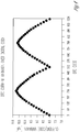
- FIG. 4 is a graph of an example of current variation versus DTC code for a DTC circuit. The graph shows the variation in current due to different values of a ten bit DTC code input to the DTC circuit. If the DTC circuit transitions from a digital value with low current demand to a different digital value with a higher current demand, the change in demand on the power supply may induce errors in the phase delay modulation.
- FIG. 5A is a graph of an example of a change in supply voltage for a DTC circuit resulting from a step change in current demand.
- the graph shows the power supply output voltage versus clock period when the digital value changes from a code of 0 to a code of 256.
- FIG. 5B is a graph showing the effect on the phase delay versus time resulting from the change in demand on the power supply in the example of FIG. 5A.
- FIG. 5B shows that it takes multiple clock cycles to settle to the programmed delay value. This settling time may cause errors in the phase modulation.
- the settling time may be a function of the response by power supply regulating circuit.
- a regulating circuit with a faster response time and hence higher bandwidth would help improve the settling time, but the faster response time may come with a cost of higher current consumption and larger circuit area.
- FIG. 6 is an embodiment of a low drop out regulator (LDO) circuit 620.
- the LDO circuit 620 is electrically coupled to a positive supply rail 650 and circuit ground.
- the LDO circuit 620 provides a direct current (DC) regulated output voltage level to DTC circuit 615 that can be very close in value to the positive voltage supply rail.
- the LDO circuit 620 includes an error amplifier circuit 655 and a cascade transistor 660 coupled to a pass gate transistor 670.
- the cascade transistor 660 and the pass gate transistor 670 are metal oxide semiconductor (MOS) transistors.
- the MOS transistors are a p-type metal oxide semiconductor (PMOS) transistors.
- the error amplifier circuit 655 senses the voltage at the output and activates the cascade transistor 660 according to a difference between a voltage at the LDO output and a reference voltage V ref .
- the output voltage is divided down using resistors 665.
- the LDO circuit 620 includes a voltage supply rail and the pass gate transistor 670 electrically coupled to the voltage supply rail 650, and current supplied to the DTC circuit 615 flows through the pass gate transistor 670.
- the regulated output of the LDO circuit 620 differs from the supply voltage only by the source-drain voltage of transistor 670.
- the LDO circuit 620 includes a slow control loop 622 that includes the cascade transistor 660, a resistor 665, and the error amplifier circuit 655.
- the LDO circuit 620 also includes fast control loop 624 that includes the cascade transistor 660 and the circuit path from the drain of the cascade transistor 660 to the gate of transistor 670.
- the slow control loop has high gain and low bandwidth and controls the absolute output voltage.
- the fast control loop has low gain and high bandwidth and regulates errors in the output voltage due to changes in the load current.
- the amount of settling time of FIG. 5B is mainly dependent on the amount of bandwidth of the fast control loop.
- the LDO circuit 620 includes an adjustable bias current.
- the LDO circuit 620 includes multiple current source circuits.
- the bias current may be programmable by activating and deactivating current sources.
- the LDO circuit includes multiple current mirrors 672 connected in parallel at the drain of the cascade transistor 660.
- the bias current can be adjusted by enabling or disabling current mirrors to set the amount of bias current.
- the bias current can be adjusted with the change in digital value.
- the current necessary for proper performance of the LDO circuit is provided, and the higher current is supplied only when determined by the programmed phase.
- the current necessary for proper performance of the LDO circuit is provided, and the higher current is supplied only when required by the programmed phase, although the scope of the embodiments is not limited in this respect.
- logic circuitry is electrically coupled to the LDO circuit and DTC circuit (e.g., logic circuitry 345 of the device in FIG. 3 ).
- the logic circuitry includes a processor circuit (e.g., a microprocessor).
- the logic circuity includes a state machine circuit. The state machine circuit sequentially steps through a fixed series of steps or states to perform one or more of the functions described. The logic for the sequence is typically implemented in hardware or firmware.
- the logic circuitry sets the adjustable bias current of the LDO circuit according to the specified digital value input to the DTC circuit.
- the logic circuitry 345 translates the digital value input to the DTC to a coded current value, and activates or deactivates the current source circuits according to the coded current value to compensate the bias point of the LDO circuit for the change in digital value.
- the logic circuitry generates both the digital value for the DTC circuit to generate the phase delay and the coded current value to program the adjustable bias current.
- the logic circuitry receives the digital value input to the DTC circuit from separate circuitry and determines the coded current value from the received digital value.
- a memory circuit 385 is electrically coupled to or integral to the logic circuitry.
- the memory circuit 385 stores a look up table containing coded current values indexed by the digital value for the delay input to the DTC circuit. The indexing translates the delay value to a coded current value.
- the logic circuitry programs the bias current circuit by enabling and disabling current source circuits according to the coded current value.
- LDO circuit compensation for the regulator circuit has been described using a specific embodiment of an LDO circuit, one skilled in the art would understand upon reading this detailed description that other LDO circuit topologies can be compensated using the approaches described herein. Additionally, the LDO circuit compensation can be used for other applications of the LDO circuit.
- FIG. 7 is a block diagram of an electronic circuit that includes a digital-to-analog converter (DAC) circuit 790 and an LDO circuit 720.
- the DAC circuit 790 converts a digital value at the input to the DAC circuit to an analog signal at an output of the DAC. Different digital values input to the DAC may result in different loads on the LDO circuit.
- the LDO circuit has adjustable bias current and the current demand for a specified digital value input to the DTC circuit is known, the bias current can be adjusted with the change in digital value (e.g., by logic circuitry).
- a lookup table stored in memory can be indexed by the digital input value to determine a coded current value used to enable and disable current mirrors to program the bias current of the LDO circuit.
- FIG. 8 illustrates, for one embodiment, example components of a User Equipment (UE) device 800.
- the UE device 800 may include application circuitry 803, baseband circuitry 806, Radio Frequency (RF) circuitry 802, front-end module (FEM) circuitry 808 and one or more antennas 801, coupled together at least as shown.
- RF Radio Frequency
- FEM front-end module
- the application circuitry 803 may include one or more application processors.
- the application circuitry 803 may include circuitry such as, but not limited to, one or more single-core or multi-core processors.
- the processor(s) may include any combination of general-purpose processors and dedicated processors (e.g., graphics processors, application processors, etc.).
- the processors may be coupled with and/or may include memory/storage and may be configured to execute instructions stored in the memory/storage to enable various applications and/or operating systems to run on the system.
- the baseband circuitry 806 may include circuitry such as, but not limited to, one or more single-core or multi-core processors.
- the baseband circuitry 806 may include one or more baseband processors and/or control logic to process baseband signals received from a receive signal path of the RF circuitry 802 and to generate baseband signals for a transmit signal path of the RF circuitry 802.
- Baseband processing circuity 806 may interface with the application circuitry 803 for generation and processing of the baseband signals and for controlling operations of the RF circuitry 802.
- the baseband circuitry 806 may include a second generation (2G) baseband processor 806a, third generation (3G) baseband processor 806b, fourth generation (4G) baseband processor 806c, and/or other baseband processor(s) 806d for other existing generations, generations in development or to be developed in the future (e.g., fifth generation (5G), 6G, etc.).
- the baseband circuitry 806 e.g., one or more of baseband processors 806a-d
- the radio control functions may include, but are not limited to, signal modulation/demodulation, encoding/decoding, radio frequency shifting, etc.
- modulation/demodulation circuitry of the baseband circuitry 806 may include Fast-Fourier Transform (FFT), precoding, and/or constellation mapping/demapping functionality.
- FFT Fast-Fourier Transform
- encoding/decoding circuitry of the baseband circuitry 806 may include convolution, tail-biting convolution, turbo, Viterbi, and/or Low Density Parity Check (LDPC) encoder/decoder functionality.
- LDPC Low Density Parity Check
- the baseband circuitry 806 may include elements of a protocol stack such as, for example, elements of an evolved universal terrestrial radio access network (E-UTRAN) protocol including, for example, physical (PHY), media access control (MAC), radio link control (RLC), packet data convergence protocol (PDCP), and/or radio resource control (RRC) elements.
- E-UTRAN evolved universal terrestrial radio access network
- a central processing unit (CPU) 806e of the baseband circuitry 806 may be configured to run elements of the protocol stack for signaling of the PHY, MAC, RLC, PDCP, and/or RRC layers.
- the baseband circuitry may include one or more audio digital signal processor(s) (DSP) 806f.
- DSP audio digital signal processor
- the audio DSP(s) 806f may be include elements for compression/decompression and echo cancellation and may include other suitable processing elements in other embodiments.
- Components of the baseband circuitry may be suitably combined in a single chip, a single chipset, or disposed on a same circuit board in some embodiments.
- some or all of the constituent components of the baseband circuitry 806 and the application circuitry 803 may be implemented together such as, for example, on a system on a chip (SOC).
- SOC system on a chip
- the baseband circuitry 806 may provide for communication compatible with one or more radio technologies.
- the baseband circuitry 806 may support communication with an evolved universal terrestrial radio access network (EUTRAN) and/or other wireless metropolitan area networks (WMAN), a wireless local area network (WLAN), a wireless personal area network (WPAN).
- EUTRAN evolved universal terrestrial radio access network
- WMAN wireless metropolitan area networks
- WLAN wireless local area network
- WPAN wireless personal area network
- multi-mode baseband circuitry Embodiments in which the baseband circuitry 806 is configured to support radio communications of more than one wireless protocol.
- RF circuitry 802 may enable communication with wireless networks using modulated electromagnetic radiation through a non-solid medium.
- the RF circuitry 802 may include switches, filters, amplifiers, etc. to facilitate the communication with the wireless network.
- RF circuitry 802 may include a receive signal path which may include circuitry to down-convert RF signals received from the FEM circuitry 808 and provide baseband signals to the baseband circuitry 806.
- RF circuitry 802 may also include a transmit signal path which may include circuitry to up-convert baseband signals provided by the baseband circuitry 806 and provide RF output signals to the FEM circuitry 808 for transmission.
- the RF circuitry 802 may include a receive signal path and a transmit signal path.
- the receive signal path of the RF circuitry 802 may include mixer circuitry 802a, amplifier circuitry 802b and filter circuitry 802c.
- the transmit signal path of the RF circuitry 802 may include filter circuitry 802c and mixer circuitry 802a.
- RF circuitry 802 may also include synthesizer circuitry 802d for synthesizing a frequency for use by the mixer circuitry 802a of the receive signal path and the transmit signal path.
- the mixer circuitry 802a of the receive signal path may be configured to down-convert RF signals received from the FEM circuitry 808 based on the synthesized frequency provided by synthesizer circuitry 802d.
- the amplifier circuitry 802b may be configured to amplify the down-converted signals and the filter circuitry 802c may be a low-pass filter (LPF) or band-pass filter (BPF) configured to remove unwanted signals from the down-converted signals to generate output baseband signals.
- LPF low-pass filter
- BPF band-pass filter
- Output baseband signals may be provided to the baseband circuitry 804 for further processing.
- the output baseband signals may be zero-frequency baseband signals, although this is not a requirement.
- mixer circuitry 802a of the receive signal path may comprise passive mixers, although the scope of the embodiments is not limited in this respect.
- the mixer circuitry 802a of the transmit signal path may be configured to up-convert input baseband signals based on the synthesized frequency provided by the synthesizer circuitry 802d to generate RF output signals for the FEM circuitry 808.
- the baseband signals may be provided by the baseband circuitry 806 and may be filtered by filter circuitry 802c.
- the filter circuitry 802c may include a low-pass filter (LPF), although the scope of the embodiments is not limited in this respect.
- LPF low-pass filter
- the mixer circuitry 802a of the receive signal path and the mixer circuitry 802a of the transmit signal path may include two or more mixers and may be arranged for quadrature downconversion and/or upconversion respectively.
- the mixer circuitry 802a of the receive signal path and the mixer circuitry 802a of the transmit signal path may include two or more mixers and may be arranged for image rejection (e.g., Hartley image rejection).
- the mixer circuitry 802a of the receive signal path and the mixer circuitry 802a may be arranged for direct downconversion and/or direct upconversion, respectively.
- the mixer circuitry 802a of the receive signal path and the mixer circuitry 802a of the transmit signal path may be configured for super-heterodyne operation.
- the output baseband signals and the input baseband signals may be analog baseband signals, although the scope of the embodiments is not limited in this respect.
- the output baseband signals and the input baseband signals may be digital baseband signals.
- the RF circuitry 802 may include analog-to-digital converter (ADC) and digital-to-analog converter (DAC) circuitry and the baseband circuitry 806 may include a digital baseband interface to communicate with the RF circuitry 802.
- ADC analog-to-digital converter
- DAC digital-to-analog converter
- a separate radio IC circuitry may be provided for processing signals for each spectrum, although the scope of the embodiments is not limited in this respect.
- the synthesizer circuitry 802d may be a fractional-N synthesizer or a fractional N/N+1 synthesizer, although the scope of the embodiments is not limited in this respect as other types of frequency synthesizers may be suitable.
- synthesizer circuitry 802d may be a delta-sigma synthesizer, a frequency multiplier, or a synthesizer comprising a phase-locked loop with a frequency divider.
- the synthesizer circuitry 802d may be configured to synthesize an output frequency for use by the mixer circuitry 802a of the RF circuitry 802 based on a frequency input and a divider control input. In some embodiments, the synthesizer circuitry 802d may be a fractional N/N+1 synthesizer.
- frequency input may be provided by a voltage controlled oscillator (VCO), although that is not a requirement.
- VCO voltage controlled oscillator
- Divider control input may be provided by either the baseband circuitry 806 or the applications processor 803 depending on the desired output frequency.
- a divider control input (e.g., N) may be determined from a look-up table based on a channel indicated by the applications processor 803.
- Synthesizer circuitry 802d of the RF circuitry 802 may include a divider, a delay-locked loop (DLL), a multiplexer and a phase accumulator.
- the divider may be a dual modulus divider (DMD) and the phase accumulator may be a digital phase accumulator (DPA).
- the DMD may be configured to divide the input signal by either N or N+1 (e.g., based on a carry out) to provide a fractional division ratio.
- the DLL may include a set of cascaded, tunable, delay elements, a phase detector, a charge pump and a D-type flip-flop.
- the delay elements may be configured to break a VCO period up into Nd equal packets of phase, where Nd is the number of delay elements in the delay line.
- Nd is the number of delay elements in the delay line.
- synthesizer circuitry 802d may be configured to generate a carrier frequency as the output frequency, while in other embodiments, the output frequency may be a multiple of the carrier frequency (e.g., twice the carrier frequency, four times the carrier frequency) and used in conjunction with quadrature generator and divider circuitry to generate multiple signals at the carrier frequency with multiple different phases with respect to each other.
- the output frequency may be a LO frequency (f LO ).
- the RF circuitry 802 may include an IQ/polar converter.
- FEM circuitry 808 may include a receive signal path which may include circuitry configured to operate on RF signals received from one or more antennas 810, amplify the received signals and provide the amplified versions of the received signals to the RF circuitry 802 for further processing.
- FEM circuitry 808 may also include a transmit signal path which may include circuitry configured to amplify signals for transmission provided by the RF circuitry 802 for transmission by one or more of the one or more antennas 810.
- the FEM circuitry 808 may include a TX/RX switch to switch between transmit mode and receive mode operation.
- the FEM circuitry may include a receive signal path and a transmit signal path.
- the receive signal path of the FEM circuitry may include a low-noise amplifier (LNA) to amplify received RF signals and provide the amplified received RF signals as an output (e.g., to the RF circuitry 802).
- the transmit signal path of the FEM circuitry 808 may include a power amplifier (PA) to amplify input RF signals (e.g., provided by RF circuitry 802), and one or more filters to generate RF signals for subsequent transmission (e.g., by one or more of the one or more antennas 810.
- PA power amplifier
- the UE device 800 may include additional elements such as, for example, memory/storage, display, camera, sensor, and/or input/output (I/O) interface.
- additional elements such as, for example, memory/storage, display, camera, sensor, and/or input/output (I/O) interface.
- the several embodiments described herein provide for power supply regulation of phase modulation in a feed forward fashion. Many of the embodiments have been described in terms of a DTC circuit, but the methods and devices can be applied to any circuit that may experience fast load current transients caused by changes in digital inputs to the circuit, such as a circuit that generates digital clock signals for example. Knowledge of the current consumption of the power supply regulator allows for modification of the control of the power supply regulator to provide a constant voltage at the output and improve power supply rejection of the phase modulation.
- Example 1 includes subject matter (such as an apparatus) comprising: radio frequency (RF) transceiver circuitry configured to transmit and receive data with a network and a mobile communication device; a phase modulator that comprises digital-to-time converter (DTC) circuitry configured to convert a digital value to a specified signal phase of a signal transmitted by the RF transceiver circuitry; low drop out regulator (LDO) circuitry operatively coupled to the DTC circuitry, wherein a bias current of the LDO is adjustable; and logic circuitry electrically coupled to the LDO circuitry and DTC circuitry, wherein the logic circuitry is configured to set the adjustable bias current of the LDO circuitry according to a digital value input to the DTC circuitry.
- RF radio frequency
- DTC digital-to-time converter
- LDO low drop out regulator
- Example 2 the subject matter of Example 1 optionally includes a memory circuit configured to store a look up table containing coded current values indexed by the digital value input to the DTC circuitry, wherein the LDO circuitry includes a programmable bias current circuit to produce the adjustable bias current, and wherein the logic circuitry is configured to set the bias current of the programmable bias current circuit using a coded current value corresponding to the digital value input to the DTC circuitry.
- Example 3 the subject matter of Example 2 optionally includes a programmable bias current circuit including multiple current source circuits connected in parallel, and wherein the logic circuitry is configured to perform one or both of activating and deactivating the current source circuits according to the coded current value.
- Example 4 the subject matter of one or any combination of Examples 1-3 optionally includes a local oscillator (LO) circuit that provides a LO signal to the DTC circuitry, wherein the DTC circuitry converts the digital value to a specified delay of the LO signal.
- LO local oscillator
- Example 5 the subject matter of Example 4 optionally includes a delay line electrically coupled to the LO circuit, wherein the delay line includes multiple unit circuit delays electrically coupled in series, and wherein the DTC circuitry is configured to apply the LO signal to a specified number of the unit circuit delays according to the digital value.
- Example 6 the subject matter of one or any combinations of Examples 1-5 optionally includes a phase modulator and a DTC circuitry included in digital polar transmitter (DPTX) circuitry configured to apply amplitude and phase modulation to the signal transmitted by the RF transceiver circuitry.
- DPTX digital polar transmitter
- Example 7 the subject matter of one or any combination of Examples 1-6 optionally includes LDO circuitry including an error amplifier circuit and a pass gate circuit that includes a first metal oxide semiconductor (MOS) transistor, wherein the error amplifier circuit is configured to activate the pass gate circuit according to a difference between a voltage at the LDO output and a reference voltage, and wherein the bias current of the LDO sets a source-drain current of the first MOS transistor.
- LDO circuitry including an error amplifier circuit and a pass gate circuit that includes a first metal oxide semiconductor (MOS) transistor, wherein the error amplifier circuit is configured to activate the pass gate circuit according to a difference between a voltage at the LDO output and a reference voltage, and wherein the bias current of the LDO sets a source-drain current of the first MOS transistor.
- MOS metal oxide semiconductor
- Example 8 the subject matter of Example 7 optionally includes LDO circuitry including a voltage supply rail and a second MOS transistor electrically connected to a voltage supply rail, and wherein the first MOS transistor is cascode connected to the second MOS transistor.
- Example 9 the subject matter of one or any combination of Examples 1-8 optionally includes LDO circuitry including a plurality of current mirrors to produce the adjustable bias current, and wherein the logic circuitry includes a state machine circuit configured to enable and disable the current mirrors according to the digital value input to the DTC circuitry.
- Example 10 the subject matter of one or any combination of Examples 1-9 optionally includes LDO circuitry including a plurality of current mirrors to produce the adjustable bias current, and wherein the logic circuitry includes a processor circuit configured to provide the digital value to the DTC circuit and to enable and disable the current mirrors according to the digital value.
- LDO circuitry including a plurality of current mirrors to produce the adjustable bias current
- the logic circuitry includes a processor circuit configured to provide the digital value to the DTC circuit and to enable and disable the current mirrors according to the digital value.
- Example 11 includes subject matter (such as an apparatus of user equipment (UE)), or can optionally be combined with the subject matter of one or any combination of Examples 1-10 to include such subject matter, comprising physical layer (PHY) circuitry, wherein the PHY circuitry includes radio frequency (RF) transceiver circuitry configured to transmit and receive data from a network or a mobile communication device; a phase modulator operatively coupled to the RF transceiver circuitry, wherein the phase modulator includes digital-to-time converter (DTC) circuitry that converts a digital value to a specified signal phase of a signal transmitted by the RF transmitter circuit; low drop out regulator (LDO) circuitry operatively coupled to the DTC circuitry, wherein a steady-state operation of the LDO circuit is adjustable; and logic circuitry electrically coupled to the LDO circuitry and DTC circuitry, wherein the logic circuitry is configured to adjust the bandwidth of the LDO circuitry according to a digital value input to the DTC circuitry.
- PHY physical layer
- RF radio frequency
- Example 12 the subject matter of Example 11 optionally includes LDO circuitry with steady state operation adjustable using an adjustable bias current, wherein the logic circuitry is configured to set the adjustable bias current to a specified bias current value according to the digital value input to the DTC circuitry.
- Example 13 the subject matter of one or both of Examples 11 and 12 optionally includes a memory circuit configured to store a look up table containing coded current values indexed by the digital value input to the DTC circuitry, wherein the LDO circuitry includes a programmable bias current circuit to produce adjustable bias current, and wherein the logic circuitry is configured to set the bias current of the programmable bias current circuit using a coded current value corresponding to the digital value input to the DTC circuitry.
- Example 14 the subject matter of Example 13 optionally includes a programmable bias current circuit including multiple current source circuits connected in parallel, and wherein the logic circuitry uses the coded current value to one or both of activate and deactivate the current source circuits.
- Example 15 the subject matter of one or any combination of Examples 11-14 optionally includes a local oscillator (LO) circuit configured to provide a LO signal to the DTC circuit, wherein the DTC circuitry converts the digital value to a specified delay of the LO signal.
- LO local oscillator
- Example 16 the subject matter of one or any combination of Examples 11-15 optionally includes digital polar transmitter (DPTX) circuitry that includes the phase modulator and the DTC circuitry.
- DPTX digital polar transmitter
- Example 17 the subject matter of one or any combination of Examples 11-17 optionally includes one or more antennas electrically coupled to the RF transceiver circuitry.
- Example 18 includes subject matter, or can optionally be combined with one or any combination of Examples 1-17 to includes such subject matter, comprising a computer readable storage medium including instructions to control processing circuitry of a mobile radio frequency (RF) communication device to cause the processing circuitry to: determine a phase for a RF signal to be transmitted by a RF transceiver of the mobile RF communication device; provide a digital value input to digital-to-time converter (DTC) circuitry to generate the determined phase for the RF signal; and set an adjustable bias current of low dropout regulator (LDO) circuitry operatively coupled to the DTC circuitry according to the digital value input to the DTC circuitry.
- RF radio frequency
- Example 19 the computer readable storage medium of claim 18 optionally includes instructions to cause the processing circuitry to: read a coded current value from a look up table indexed by the digital value input to the DTC circuitry; and set the adjustable bias current of the LDO circuitry using the coded current value corresponding to the digital value input to the DTC circuitry.
- Example 20 the computer readable storage medium of claim 18 optionally includes instructions to cause the processing circuitry to generate the determined phase by applying a specified time delay to a local oscillator signal according to the digital value input to the DTC circuitry.
- Example 21 includes subject matter (such as a method of controlling operation of a mobile radio frequency (RF) communication device), or can optionally be combined with one or any combination of Examples 1-20 to includes such subject matter, comprising determining a phase for a RF signal to be transmitted by a RF transceiver of the mobile RF communication device; providing a digital value input to digital-to-time converter (DTC) circuitry to generate the determined phase for the RF signal; and setting an adjustable bias current of low dropout regulator (LDO) circuitry electrically coupled to the DTC circuitry according to the digital value input to the DTC circuitry.
- DTC digital-to-time converter
- LDO adjustable bias current of low dropout regulator
- Example 22 the subject matter of Example 21 optionally includes reading a coded current value from a look up table indexed by the digital value input to the DTC circuitry; and setting the adjustable bias current of the LDO circuitry using the coded current value corresponding to the digital value input to the DTC circuitry.
- Example 23 the subject matter of one or both of Examples 21 and 22 optionally includes generating the determined phase by applying a specified time delay to a local oscillator signal according to the digital value input to the DTC circuitry.
- Example 24 includes subject matter (such as an apparatus), or can optionally be combined with any portion or combination of any portions of any one or more of Examples 1-23 to include such subject matter, comprising: means for determining a phase for a RF signal to be transmitted by a RF transceiver of the mobile RF communication device; means for generating a digital value for input to digital-to-time converter (DTC) circuitry to generate the determined phase for the RF signal by; and means for setting an adjustable bias current of low dropout regulator (LDO) circuitry electrically coupled to the DTC circuitry according to the digital value input to the DTC circuitry.
- DTC digital-to-time converter
- LDO adjustable bias current of low dropout regulator
- Example 25 the subject matter of Example 24 optionally includes means for reading a coded current value from a look up table indexed by the digital value input to the DTC circuitry, wherein the means for setting the adjustable bias current includes means for setting the adjustable bias current of the LDO circuitry using the coded current value corresponding to the digital value input to the DTC circuitry.
- Example 26 the subject matter of one or both of Examples 24 and 25 optionally includes DTC circuitry configured to generate the determined phase by applying a specified time delay to a local oscillator signal according to the digital value input to the DTC circuitry.
- Example 27 includes subject matter (such as an apparatus), or can optionally be combined with one or any combination of Examples 1-26 to include such subject matter comprising: a local oscillator (LO) circuit that provides a LO signal; digital-to-time converter (DTC) circuitry operatively coupled to the LO circuit and configured to convert a received digital value to a specified value of signal phase of the LO signal; and low drop out regulator (LDO) circuitry operatively coupled to the DTC circuitry, wherein the LDO circuitry includes a plurality of current mirrors to produce an adjustable bias current of the LDO circuitry and a value of the bias current of the LDO is determined according to the digital value received by the DTC circuitry.
- LO local oscillator
- DTC digital-to-time converter
- LDO low drop out regulator
- Example 28 the subject matter of Example 27 optionally includes LDO circuitry that includes an error amplifier circuit and a pass gate circuit that includes a first metal oxide semiconductor (MOS) transistor, wherein the error amplifier circuit is configured to activate the pass gate circuit according to a difference between a voltage at the LDO output and a reference voltage, and wherein the bias current of the LDO sets a source-drain current of the first MOS transistor.
- LDO circuitry that includes an error amplifier circuit and a pass gate circuit that includes a first metal oxide semiconductor (MOS) transistor, wherein the error amplifier circuit is configured to activate the pass gate circuit according to a difference between a voltage at the LDO output and a reference voltage, and wherein the bias current of the LDO sets a source-drain current of the first MOS transistor.
- MOS metal oxide semiconductor
- Example 29 the subject matter of one or both of Examples 27 and 28 optionally includes LDO circuitry that includes a voltage supply rail and a second MOS transistor electrically connected to a voltage supply rail, and wherein the first MOS transistor is cascode connected to the second MOS transistor.
- Example 30 the subject matter of one or any combination of Examples 27-29 optionally includes a state machine circuit configured to enable and disable the current mirrors according to the digital value input to the DTC circuitry.
- Method examples described herein can be machine or computer-implemented at least in part. Some examples can include a computer-readable storage medium or machine-readable storage medium encoded with instructions operable to configure an electronic device to perform methods as described in the above examples.
- An implementation of such methods can include code, such as microcode, assembly language code, a higher-level language code, or the like. Such code can include computer readable instructions for performing various methods. The code may form portions of computer program products. The code can be tangibly stored on one or more volatile, non-transitory, or non-volatile tangible computer-readable media, such as during execution or at other times.
- tangible computer-readable storage media can include, but are not limited to, hard disks, removable magnetic disks, removable optical disks (e.g., compact disks and digital video disks), magnetic cassettes, memory cards or sticks, random access memories (RAMs), read only memories (ROMs), and the like.
Landscapes
- Engineering & Computer Science (AREA)
- Physics & Mathematics (AREA)
- Computer Networks & Wireless Communication (AREA)
- Signal Processing (AREA)
- Electromagnetism (AREA)
- General Physics & Mathematics (AREA)
- Radar, Positioning & Navigation (AREA)
- Automation & Control Theory (AREA)
- Microelectronics & Electronic Packaging (AREA)
- Nonlinear Science (AREA)
- Transmitters (AREA)
Abstract
Description
- Embodiments pertain to radio frequency circuits for wireless communications. Some embodiments relate to phase modulator circuits in transceiver architectures. Some embodiments relate to reducing sensitivity of circuits that use power supply regulation to fast load current transients triggered by changes in digital inputs to the circuits.
- Radio frequency (RF) devices are used for voice and data communication. Some RF devices are mobile devices (e.g., cellular phones) that are battery powered. Because RF devices do not typically have equal current consumption all of the time, RF devices generally have regulated power supplies. However, some circuits of RF devices can have poor power supply rejection. Thus, there are general needs for devices, systems and methods for RF circuits that provide robust performance by either reducing power supply disturbances or not being negatively impacted by power supply disturbances.
-
-
FIG. 1 is a block diagram of portions of a radio frequency communication device in accordance with some embodiments; -
FIG. 2 is a timing diagram of a local oscillator signal at the output of a digital-to-time converter (DTC) circuit in accordance with some embodiments; -
FIG. 3 is a circuit block diagram of portions of an embodiment of a DTC circuit in accordance with some embodiments; -
FIG. 4 is a graph of an example of current variation versus DTC code for a DTC circuit in accordance with some embodiments; -
FIG. 5A is a graph of an example of a change in supply voltage for a DTC circuit resulting from a step change in current demand; -
FIG. 5B is a graph showing the effect on the phase delay versus time resulting from the change in demand on the power supply inFIG. 5A ; -
FIG. 6 is an embodiment of a low drop out regulator circuit in accordance with some embodiments; -
FIG. 7 is a block diagram of an electronic circuit that includes a digital-to-analog converter circuit and a low dropout regulator circuit in accordance with some embodiments; -
FIG. 8 illustrates example components of a UE device in accordance with some embodiments. - The following description and the drawings sufficiently illustrate specific embodiments to enable those skilled in the art to practice them. Other embodiments may incorporate structural, logical, electrical, process, and other changes. Portions and features of some embodiments may be included in, or substituted for, those of other embodiments. Embodiments set forth in the claims encompass all available equivalents of those claims.
- RF devices that communicate using a radio access network can include digital polar transmitter (DPTX) circuit architectures. A DPTX circuit uses polar coordinates (e.g., amplitude and phase) rather than Cartesian coordinates (e.g., I and Q coordinates) for RF signal modulation. A DPTX approach offers advantages in size and power consumption over analog radio transmitter architectures. A DPTX circuit may include a digital-to-time converter (DTC) to provide phase modulation to transmitted signals. The DTC modulates a local oscillator (LO) signal with phase information using only digital circuits. This can reduce the number of inductors needed for the RF transmitter which leads to reduced size.
-
FIG. 1 is a block diagram of portions of an embodiment of anRF device 100 for communication using a radio access network. In certain embodiments, the RF device can be user equipment (UE) for a cellular communication network. The device includes anRF transceiver circuit 105. The RF transceiver circuit can include aphase modulator 110 andamplitude modulator 112. One ormore antennas 107 may be electrically coupled to theRF transceiver circuit 105. Thephase modulator 110 includes aDTC circuit 115 operatively coupled to apower supply circuit 120. TheDTC circuit 115 receives a digital value at an input and converts the digital value to a specified signal phase of a signal transmitted by the RF transceiver circuit. Thepower supply circuit 120 provides a regulated supply voltage to thephase modulator 110 andDTC circuit 115. In some embodiments, the RF device includes a local oscillator (LO)circuit 125 that provides a LO signal to theDTC circuit 115, and theDTC circuit 115 converts the digital value to a specified delay of the LO signal. -
FIG. 2 is a timing diagram of the LO signal at the output of the DTC circuit. The DTC code is the digital value input to the DTC circuit and the waveforms show the resulting DTC output signal. Three DTC code examples are shown inFIG. 2 . For the top waveform, the DTC code is 0 for a delay of 0 corresponding to a phase of 0°. The middle waveform shows the example for a DTC code for a delay of 12.5% corresponding to a phase of 45° or π/4. The bottom waveform shows the example for a DTC code for a delay of 25% corresponding to a phase of 90° or π/2. An RF signal to be transmitted may be modulated onto the phase modulated LO signal. In certain embodiments, theamplitude modulator 112 includes a digital power amplifier (DPA) to modulate the amplitude of the signal to be transmitted onto the phase modulated LO signal. -
FIG. 3 is a circuit block diagram of portions of an embodiment of aDTC circuit 315. The DTC circuit includes adelay line 330 electrically coupled to aLO circuit 325. Thedelay line 330 may include multipleunit circuit delays 335 electrically coupled in series. TheDTC circuit 315 applies theLO signal 327 to a specified number of the unit circuit delays to generate the phase modulated signal. The embodiment shown inFIG. 3 includes amultiplexer circuit 340 andlogic circuitry 345. The number of delays applied to the LO signal can be selected using the multiplexer circuit 340 (or Mux) andlogic circuitry 345. For example, thelogic circuitry 345 may output a digital value to themultiplexer circuit 340. The digital value determines which tap of the delay line provides the phase modulated signal at the output. - A
DTC circuit 315 may have poor power supply rejection. Changes in the supply voltage provided to the DTC circuit can be manifested on the phase signal at the output of the DTC circuit. This can lead to errors in the phase modulation. One source of the errors is the variable current consumption of the DTC circuit. Different phase delays programmed in the DTC circuit by changing the digital value input to the DTC circuit may involve different levels of current consumption.FIG. 4 is a graph of an example of current variation versus DTC code for a DTC circuit. The graph shows the variation in current due to different values of a ten bit DTC code input to the DTC circuit. If the DTC circuit transitions from a digital value with low current demand to a different digital value with a higher current demand, the change in demand on the power supply may induce errors in the phase delay modulation. -
FIG. 5A is a graph of an example of a change in supply voltage for a DTC circuit resulting from a step change in current demand. The graph shows the power supply output voltage versus clock period when the digital value changes from a code of 0 to a code of 256.FIG. 5B is a graph showing the effect on the phase delay versus time resulting from the change in demand on the power supply in the example ofFIG. 5A. FIG. 5B shows that it takes multiple clock cycles to settle to the programmed delay value. This settling time may cause errors in the phase modulation. The settling time may be a function of the response by power supply regulating circuit. A regulating circuit with a faster response time and hence higher bandwidth would help improve the settling time, but the faster response time may come with a cost of higher current consumption and larger circuit area. -
FIG. 6 is an embodiment of a low drop out regulator (LDO)circuit 620. TheLDO circuit 620 is electrically coupled to apositive supply rail 650 and circuit ground. TheLDO circuit 620 provides a direct current (DC) regulated output voltage level toDTC circuit 615 that can be very close in value to the positive voltage supply rail. TheLDO circuit 620 includes anerror amplifier circuit 655 and acascade transistor 660 coupled to apass gate transistor 670. InFIG. 6 , thecascade transistor 660 and thepass gate transistor 670 are metal oxide semiconductor (MOS) transistors. In the embodiment inFIG. 6 , the MOS transistors are a p-type metal oxide semiconductor (PMOS) transistors. Theerror amplifier circuit 655 senses the voltage at the output and activates thecascade transistor 660 according to a difference between a voltage at the LDO output and a reference voltage Vref. In the embodiment shown inFIG. 6 , the output voltage is divided down usingresistors 665. TheLDO circuit 620 includes a voltage supply rail and thepass gate transistor 670 electrically coupled to thevoltage supply rail 650, and current supplied to theDTC circuit 615 flows through thepass gate transistor 670. The regulated output of theLDO circuit 620 differs from the supply voltage only by the source-drain voltage oftransistor 670. - The
LDO circuit 620 includes aslow control loop 622 that includes thecascade transistor 660, aresistor 665, and theerror amplifier circuit 655. TheLDO circuit 620 also includesfast control loop 624 that includes thecascade transistor 660 and the circuit path from the drain of thecascade transistor 660 to the gate oftransistor 670. The slow control loop has high gain and low bandwidth and controls the absolute output voltage. The fast control loop has low gain and high bandwidth and regulates errors in the output voltage due to changes in the load current. The amount of settling time ofFIG. 5B is mainly dependent on the amount of bandwidth of the fast control loop. - The
LDO circuit 620 includes an adjustable bias current. In some embodiments, theLDO circuit 620 includes multiple current source circuits. The bias current may be programmable by activating and deactivating current sources. In the embodiment ofFIG. 6 , the LDO circuit includes multiplecurrent mirrors 672 connected in parallel at the drain of thecascade transistor 660. The bias current can be adjusted by enabling or disabling current mirrors to set the amount of bias current. As explained previously, when a change in the digital input triggers a fast transient in load current, the regulation of the LDO circuit would bring the fast and slow control loops to steady-state operation after a settling time. Changing the bias current brings the fast and slow control loops close to their steady-state operation more quickly. If the current consumption or current demand for a specified digital value input to the DTC circuit is known, the bias current can be adjusted with the change in digital value. In some of these embodiments, the current necessary for proper performance of the LDO circuit is provided, and the higher current is supplied only when determined by the programmed phase. In some embodiments, the current necessary for proper performance of the LDO circuit is provided, and the higher current is supplied only when required by the programmed phase, although the scope of the embodiments is not limited in this respect. - In some embodiments, logic circuitry is electrically coupled to the LDO circuit and DTC circuit (e.g.,
logic circuitry 345 of the device inFIG. 3 ). In certain embodiments, the logic circuitry includes a processor circuit (e.g., a microprocessor). In certain embodiments, the logic circuity includes a state machine circuit. The state machine circuit sequentially steps through a fixed series of steps or states to perform one or more of the functions described. The logic for the sequence is typically implemented in hardware or firmware. - The logic circuitry sets the adjustable bias current of the LDO circuit according to the specified digital value input to the DTC circuit. In some embodiments, the
logic circuitry 345 translates the digital value input to the DTC to a coded current value, and activates or deactivates the current source circuits according to the coded current value to compensate the bias point of the LDO circuit for the change in digital value. In certain embodiments, the logic circuitry generates both the digital value for the DTC circuit to generate the phase delay and the coded current value to program the adjustable bias current. In certain embodiments, the logic circuitry receives the digital value input to the DTC circuit from separate circuitry and determines the coded current value from the received digital value. - In some embodiments, a
memory circuit 385 is electrically coupled to or integral to the logic circuitry. Thememory circuit 385 stores a look up table containing coded current values indexed by the digital value for the delay input to the DTC circuit. The indexing translates the delay value to a coded current value. The logic circuitry programs the bias current circuit by enabling and disabling current source circuits according to the coded current value. - Although the compensation for the regulator circuit has been described using a specific embodiment of an LDO circuit, one skilled in the art would understand upon reading this detailed description that other LDO circuit topologies can be compensated using the approaches described herein. Additionally, the LDO circuit compensation can be used for other applications of the LDO circuit.
-
FIG. 7 is a block diagram of an electronic circuit that includes a digital-to-analog converter (DAC)circuit 790 and anLDO circuit 720. TheDAC circuit 790 converts a digital value at the input to the DAC circuit to an analog signal at an output of the DAC. Different digital values input to the DAC may result in different loads on the LDO circuit. If the LDO circuit has adjustable bias current and the current demand for a specified digital value input to the DTC circuit is known, the bias current can be adjusted with the change in digital value (e.g., by logic circuitry). As with the DTC circuit, a lookup table stored in memory can be indexed by the digital input value to determine a coded current value used to enable and disable current mirrors to program the bias current of the LDO circuit. - Embodiments described herein may be implemented into a system using any suitably configured hardware and/or software.
FIG. 8 illustrates, for one embodiment, example components of a User Equipment (UE)device 800. In some embodiments, theUE device 800 may includeapplication circuitry 803,baseband circuitry 806, Radio Frequency (RF)circuitry 802, front-end module (FEM)circuitry 808 and one or more antennas 801, coupled together at least as shown. - The
application circuitry 803 may include one or more application processors. For example, theapplication circuitry 803 may include circuitry such as, but not limited to, one or more single-core or multi-core processors. The processor(s) may include any combination of general-purpose processors and dedicated processors (e.g., graphics processors, application processors, etc.). The processors may be coupled with and/or may include memory/storage and may be configured to execute instructions stored in the memory/storage to enable various applications and/or operating systems to run on the system. - The
baseband circuitry 806 may include circuitry such as, but not limited to, one or more single-core or multi-core processors. Thebaseband circuitry 806 may include one or more baseband processors and/or control logic to process baseband signals received from a receive signal path of theRF circuitry 802 and to generate baseband signals for a transmit signal path of theRF circuitry 802.Baseband processing circuity 806 may interface with theapplication circuitry 803 for generation and processing of the baseband signals and for controlling operations of theRF circuitry 802. For example, in some embodiments, thebaseband circuitry 806 may include a second generation (2G) baseband processor 806a, third generation (3G) baseband processor 806b, fourth generation (4G) baseband processor 806c, and/or other baseband processor(s) 806d for other existing generations, generations in development or to be developed in the future (e.g., fifth generation (5G), 6G, etc.). The baseband circuitry 806 (e.g., one or more of baseband processors 806a-d) may handle various radio control functions that enable communication with one or more radio networks via theRF circuitry 802. The radio control functions may include, but are not limited to, signal modulation/demodulation, encoding/decoding, radio frequency shifting, etc. In some embodiments, modulation/demodulation circuitry of thebaseband circuitry 806 may include Fast-Fourier Transform (FFT), precoding, and/or constellation mapping/demapping functionality. In some embodiments, encoding/decoding circuitry of thebaseband circuitry 806 may include convolution, tail-biting convolution, turbo, Viterbi, and/or Low Density Parity Check (LDPC) encoder/decoder functionality. Embodiments of modulation/demodulation and encoder/decoder functionality are not limited to these examples and may include other suitable functionality in other embodiments. - In some embodiments, the
baseband circuitry 806 may include elements of a protocol stack such as, for example, elements of an evolved universal terrestrial radio access network (E-UTRAN) protocol including, for example, physical (PHY), media access control (MAC), radio link control (RLC), packet data convergence protocol (PDCP), and/or radio resource control (RRC) elements. A central processing unit (CPU) 806e of thebaseband circuitry 806 may be configured to run elements of the protocol stack for signaling of the PHY, MAC, RLC, PDCP, and/or RRC layers. In some embodiments, the baseband circuitry may include one or more audio digital signal processor(s) (DSP) 806f. The audio DSP(s) 806f may be include elements for compression/decompression and echo cancellation and may include other suitable processing elements in other embodiments. Components of the baseband circuitry may be suitably combined in a single chip, a single chipset, or disposed on a same circuit board in some embodiments. In some embodiments, some or all of the constituent components of thebaseband circuitry 806 and theapplication circuitry 803 may be implemented together such as, for example, on a system on a chip (SOC). - In some embodiments, the
baseband circuitry 806 may provide for communication compatible with one or more radio technologies. For example, in some embodiments, thebaseband circuitry 806 may support communication with an evolved universal terrestrial radio access network (EUTRAN) and/or other wireless metropolitan area networks (WMAN), a wireless local area network (WLAN), a wireless personal area network (WPAN). Embodiments in which thebaseband circuitry 806 is configured to support radio communications of more than one wireless protocol may be referred to as multi-mode baseband circuitry. -
RF circuitry 802 may enable communication with wireless networks using modulated electromagnetic radiation through a non-solid medium. In various embodiments, theRF circuitry 802 may include switches, filters, amplifiers, etc. to facilitate the communication with the wireless network.RF circuitry 802 may include a receive signal path which may include circuitry to down-convert RF signals received from theFEM circuitry 808 and provide baseband signals to thebaseband circuitry 806.RF circuitry 802 may also include a transmit signal path which may include circuitry to up-convert baseband signals provided by thebaseband circuitry 806 and provide RF output signals to theFEM circuitry 808 for transmission. - In some embodiments, the
RF circuitry 802 may include a receive signal path and a transmit signal path. The receive signal path of theRF circuitry 802 may include mixer circuitry 802a, amplifier circuitry 802b and filter circuitry 802c. The transmit signal path of theRF circuitry 802 may include filter circuitry 802c and mixer circuitry 802a.RF circuitry 802 may also include synthesizer circuitry 802d for synthesizing a frequency for use by the mixer circuitry 802a of the receive signal path and the transmit signal path. In some embodiments, the mixer circuitry 802a of the receive signal path may be configured to down-convert RF signals received from theFEM circuitry 808 based on the synthesized frequency provided by synthesizer circuitry 802d. The amplifier circuitry 802b may be configured to amplify the down-converted signals and the filter circuitry 802c may be a low-pass filter (LPF) or band-pass filter (BPF) configured to remove unwanted signals from the down-converted signals to generate output baseband signals. Output baseband signals may be provided to the baseband circuitry 804 for further processing. In some embodiments, the output baseband signals may be zero-frequency baseband signals, although this is not a requirement. In some embodiments, mixer circuitry 802a of the receive signal path may comprise passive mixers, although the scope of the embodiments is not limited in this respect. - In some embodiments, the mixer circuitry 802a of the transmit signal path may be configured to up-convert input baseband signals based on the synthesized frequency provided by the synthesizer circuitry 802d to generate RF output signals for the
FEM circuitry 808. The baseband signals may be provided by thebaseband circuitry 806 and may be filtered by filter circuitry 802c. The filter circuitry 802c may include a low-pass filter (LPF), although the scope of the embodiments is not limited in this respect. - In some embodiments, the mixer circuitry 802a of the receive signal path and the mixer circuitry 802a of the transmit signal path may include two or more mixers and may be arranged for quadrature downconversion and/or upconversion respectively. In some embodiments, the mixer circuitry 802a of the receive signal path and the mixer circuitry 802a of the transmit signal path may include two or more mixers and may be arranged for image rejection (e.g., Hartley image rejection). In some embodiments, the mixer circuitry 802a of the receive signal path and the mixer circuitry 802a may be arranged for direct downconversion and/or direct upconversion, respectively. In some embodiments, the mixer circuitry 802a of the receive signal path and the mixer circuitry 802a of the transmit signal path may be configured for super-heterodyne operation.
- In some embodiments, the output baseband signals and the input baseband signals may be analog baseband signals, although the scope of the embodiments is not limited in this respect. In some alternate embodiments, the output baseband signals and the input baseband signals may be digital baseband signals. In these alternate embodiments, the
RF circuitry 802 may include analog-to-digital converter (ADC) and digital-to-analog converter (DAC) circuitry and thebaseband circuitry 806 may include a digital baseband interface to communicate with theRF circuitry 802. - In some dual-mode embodiments, a separate radio IC circuitry may be provided for processing signals for each spectrum, although the scope of the embodiments is not limited in this respect.
- In some embodiments, the synthesizer circuitry 802d may be a fractional-N synthesizer or a fractional N/N+1 synthesizer, although the scope of the embodiments is not limited in this respect as other types of frequency synthesizers may be suitable. For example, synthesizer circuitry 802d may be a delta-sigma synthesizer, a frequency multiplier, or a synthesizer comprising a phase-locked loop with a frequency divider.
- The synthesizer circuitry 802d may be configured to synthesize an output frequency for use by the mixer circuitry 802a of the
RF circuitry 802 based on a frequency input and a divider control input. In some embodiments, the synthesizer circuitry 802d may be a fractional N/N+1 synthesizer. - In some embodiments, frequency input may be provided by a voltage controlled oscillator (VCO), although that is not a requirement. Divider control input may be provided by either the
baseband circuitry 806 or theapplications processor 803 depending on the desired output frequency. In some embodiments, a divider control input (e.g., N) may be determined from a look-up table based on a channel indicated by theapplications processor 803. - Synthesizer circuitry 802d of the
RF circuitry 802 may include a divider, a delay-locked loop (DLL), a multiplexer and a phase accumulator. In some embodiments, the divider may be a dual modulus divider (DMD) and the phase accumulator may be a digital phase accumulator (DPA). In some embodiments, the DMD may be configured to divide the input signal by either N or N+1 (e.g., based on a carry out) to provide a fractional division ratio. In some example embodiments, the DLL may include a set of cascaded, tunable, delay elements, a phase detector, a charge pump and a D-type flip-flop. In these embodiments, the delay elements may be configured to break a VCO period up into Nd equal packets of phase, where Nd is the number of delay elements in the delay line. In this way, the DLL provides negative feedback to help ensure that the total delay through the delay line is one VCO cycle. - In some embodiments, synthesizer circuitry 802d may be configured to generate a carrier frequency as the output frequency, while in other embodiments, the output frequency may be a multiple of the carrier frequency (e.g., twice the carrier frequency, four times the carrier frequency) and used in conjunction with quadrature generator and divider circuitry to generate multiple signals at the carrier frequency with multiple different phases with respect to each other. In some embodiments, the output frequency may be a LO frequency (fLO). In some embodiments, the
RF circuitry 802 may include an IQ/polar converter. -
FEM circuitry 808 may include a receive signal path which may include circuitry configured to operate on RF signals received from one ormore antennas 810, amplify the received signals and provide the amplified versions of the received signals to theRF circuitry 802 for further processing.FEM circuitry 808 may also include a transmit signal path which may include circuitry configured to amplify signals for transmission provided by theRF circuitry 802 for transmission by one or more of the one ormore antennas 810. - In some embodiments, the
FEM circuitry 808 may include a TX/RX switch to switch between transmit mode and receive mode operation. The FEM circuitry may include a receive signal path and a transmit signal path. The receive signal path of the FEM circuitry may include a low-noise amplifier (LNA) to amplify received RF signals and provide the amplified received RF signals as an output (e.g., to the RF circuitry 802). The transmit signal path of theFEM circuitry 808 may include a power amplifier (PA) to amplify input RF signals (e.g., provided by RF circuitry 802), and one or more filters to generate RF signals for subsequent transmission (e.g., by one or more of the one ormore antennas 810. - In some embodiments, the
UE device 800 may include additional elements such as, for example, memory/storage, display, camera, sensor, and/or input/output (I/O) interface. - The several embodiments described herein provide for power supply regulation of phase modulation in a feed forward fashion. Many of the embodiments have been described in terms of a DTC circuit, but the methods and devices can be applied to any circuit that may experience fast load current transients caused by changes in digital inputs to the circuit, such as a circuit that generates digital clock signals for example. Knowledge of the current consumption of the power supply regulator allows for modification of the control of the power supply regulator to provide a constant voltage at the output and improve power supply rejection of the phase modulation.
- Example 1 includes subject matter (such as an apparatus) comprising: radio frequency (RF) transceiver circuitry configured to transmit and receive data with a network and a mobile communication device; a phase modulator that comprises digital-to-time converter (DTC) circuitry configured to convert a digital value to a specified signal phase of a signal transmitted by the RF transceiver circuitry; low drop out regulator (LDO) circuitry operatively coupled to the DTC circuitry, wherein a bias current of the LDO is adjustable; and logic circuitry electrically coupled to the LDO circuitry and DTC circuitry, wherein the logic circuitry is configured to set the adjustable bias current of the LDO circuitry according to a digital value input to the DTC circuitry.
- In Example 2, the subject matter of Example 1 optionally includes a memory circuit configured to store a look up table containing coded current values indexed by the digital value input to the DTC circuitry, wherein the LDO circuitry includes a programmable bias current circuit to produce the adjustable bias current, and wherein the logic circuitry is configured to set the bias current of the programmable bias current circuit using a coded current value corresponding to the digital value input to the DTC circuitry.
- In Example 3, the subject matter of Example 2 optionally includes a programmable bias current circuit including multiple current source circuits connected in parallel, and wherein the logic circuitry is configured to perform one or both of activating and deactivating the current source circuits according to the coded current value.
- In Example 4, the subject matter of one or any combination of Examples 1-3 optionally includes a local oscillator (LO) circuit that provides a LO signal to the DTC circuitry, wherein the DTC circuitry converts the digital value to a specified delay of the LO signal.
- In Example 5, the subject matter of Example 4 optionally includes a delay line electrically coupled to the LO circuit, wherein the delay line includes multiple unit circuit delays electrically coupled in series, and wherein the DTC circuitry is configured to apply the LO signal to a specified number of the unit circuit delays according to the digital value.
- In Example 6, the subject matter of one or any combinations of Examples 1-5 optionally includes a phase modulator and a DTC circuitry included in digital polar transmitter (DPTX) circuitry configured to apply amplitude and phase modulation to the signal transmitted by the RF transceiver circuitry.
- In Example 7, the subject matter of one or any combination of Examples 1-6 optionally includes LDO circuitry including an error amplifier circuit and a pass gate circuit that includes a first metal oxide semiconductor (MOS) transistor, wherein the error amplifier circuit is configured to activate the pass gate circuit according to a difference between a voltage at the LDO output and a reference voltage, and wherein the bias current of the LDO sets a source-drain current of the first MOS transistor.
- In Example 8, the subject matter of Example 7 optionally includes LDO circuitry including a voltage supply rail and a second MOS transistor electrically connected to a voltage supply rail, and wherein the first MOS transistor is cascode connected to the second MOS transistor.
- In Example 9, the subject matter of one or any combination of Examples 1-8 optionally includes LDO circuitry including a plurality of current mirrors to produce the adjustable bias current, and wherein the logic circuitry includes a state machine circuit configured to enable and disable the current mirrors according to the digital value input to the DTC circuitry.
- In Example 10, the subject matter of one or any combination of Examples 1-9 optionally includes LDO circuitry including a plurality of current mirrors to produce the adjustable bias current, and wherein the logic circuitry includes a processor circuit configured to provide the digital value to the DTC circuit and to enable and disable the current mirrors according to the digital value.
- Example 11 includes subject matter (such as an apparatus of user equipment (UE)), or can optionally be combined with the subject matter of one or any combination of Examples 1-10 to include such subject matter, comprising physical layer (PHY) circuitry, wherein the PHY circuitry includes radio frequency (RF) transceiver circuitry configured to transmit and receive data from a network or a mobile communication device; a phase modulator operatively coupled to the RF transceiver circuitry, wherein the phase modulator includes digital-to-time converter (DTC) circuitry that converts a digital value to a specified signal phase of a signal transmitted by the RF transmitter circuit; low drop out regulator (LDO) circuitry operatively coupled to the DTC circuitry, wherein a steady-state operation of the LDO circuit is adjustable; and logic circuitry electrically coupled to the LDO circuitry and DTC circuitry, wherein the logic circuitry is configured to adjust the bandwidth of the LDO circuitry according to a digital value input to the DTC circuitry.
- In Example 12, the subject matter of Example 11 optionally includes LDO circuitry with steady state operation adjustable using an adjustable bias current, wherein the logic circuitry is configured to set the adjustable bias current to a specified bias current value according to the digital value input to the DTC circuitry.
- In Example 13, the subject matter of one or both of Examples 11 and 12 optionally includes a memory circuit configured to store a look up table containing coded current values indexed by the digital value input to the DTC circuitry, wherein the LDO circuitry includes a programmable bias current circuit to produce adjustable bias current, and wherein the logic circuitry is configured to set the bias current of the programmable bias current circuit using a coded current value corresponding to the digital value input to the DTC circuitry.
- In Example 14, the subject matter of Example 13 optionally includes a programmable bias current circuit including multiple current source circuits connected in parallel, and wherein the logic circuitry uses the coded current value to one or both of activate and deactivate the current source circuits.
- In Example 15, the subject matter of one or any combination of Examples 11-14 optionally includes a local oscillator (LO) circuit configured to provide a LO signal to the DTC circuit, wherein the DTC circuitry converts the digital value to a specified delay of the LO signal.
- In Example 16, the subject matter of one or any combination of Examples 11-15 optionally includes digital polar transmitter (DPTX) circuitry that includes the phase modulator and the DTC circuitry.
- In Example 17, the subject matter of one or any combination of Examples 11-17 optionally includes one or more antennas electrically coupled to the RF transceiver circuitry.
- Example 18 includes subject matter, or can optionally be combined with one or any combination of Examples 1-17 to includes such subject matter, comprising a computer readable storage medium including instructions to control processing circuitry of a mobile radio frequency (RF) communication device to cause the processing circuitry to: determine a phase for a RF signal to be transmitted by a RF transceiver of the mobile RF communication device; provide a digital value input to digital-to-time converter (DTC) circuitry to generate the determined phase for the RF signal; and set an adjustable bias current of low dropout regulator (LDO) circuitry operatively coupled to the DTC circuitry according to the digital value input to the DTC circuitry.
- In Example 19, the computer readable storage medium of claim 18 optionally includes instructions to cause the processing circuitry to: read a coded current value from a look up table indexed by the digital value input to the DTC circuitry; and set the adjustable bias current of the LDO circuitry using the coded current value corresponding to the digital value input to the DTC circuitry.
- In Example 20, the computer readable storage medium of claim 18 optionally includes instructions to cause the processing circuitry to generate the determined phase by applying a specified time delay to a local oscillator signal according to the digital value input to the DTC circuitry.
- Example 21 includes subject matter (such as a method of controlling operation of a mobile radio frequency (RF) communication device), or can optionally be combined with one or any combination of Examples 1-20 to includes such subject matter, comprising determining a phase for a RF signal to be transmitted by a RF transceiver of the mobile RF communication device; providing a digital value input to digital-to-time converter (DTC) circuitry to generate the determined phase for the RF signal; and setting an adjustable bias current of low dropout regulator (LDO) circuitry electrically coupled to the DTC circuitry according to the digital value input to the DTC circuitry.
- In Example 22, the subject matter of Example 21 optionally includes reading a coded current value from a look up table indexed by the digital value input to the DTC circuitry; and setting the adjustable bias current of the LDO circuitry using the coded current value corresponding to the digital value input to the DTC circuitry.
- In Example 23, the subject matter of one or both of Examples 21 and 22 optionally includes generating the determined phase by applying a specified time delay to a local oscillator signal according to the digital value input to the DTC circuitry.
- Example 24 includes subject matter (such as an apparatus), or can optionally be combined with any portion or combination of any portions of any one or more of Examples 1-23 to include such subject matter, comprising: means for determining a phase for a RF signal to be transmitted by a RF transceiver of the mobile RF communication device; means for generating a digital value for input to digital-to-time converter (DTC) circuitry to generate the determined phase for the RF signal by; and means for setting an adjustable bias current of low dropout regulator (LDO) circuitry electrically coupled to the DTC circuitry according to the digital value input to the DTC circuitry.
- In Example 25, the subject matter of Example 24 optionally includes means for reading a coded current value from a look up table indexed by the digital value input to the DTC circuitry, wherein the means for setting the adjustable bias current includes means for setting the adjustable bias current of the LDO circuitry using the coded current value corresponding to the digital value input to the DTC circuitry.
- In Example 26, the subject matter of one or both of Examples 24 and 25 optionally includes DTC circuitry configured to generate the determined phase by applying a specified time delay to a local oscillator signal according to the digital value input to the DTC circuitry.
- Example 27 includes subject matter (such as an apparatus), or can optionally be combined with one or any combination of Examples 1-26 to include such subject matter comprising: a local oscillator (LO) circuit that provides a LO signal; digital-to-time converter (DTC) circuitry operatively coupled to the LO circuit and configured to convert a received digital value to a specified value of signal phase of the LO signal; and low drop out regulator (LDO) circuitry operatively coupled to the DTC circuitry, wherein the LDO circuitry includes a plurality of current mirrors to produce an adjustable bias current of the LDO circuitry and a value of the bias current of the LDO is determined according to the digital value received by the DTC circuitry.
- In Example 28, the subject matter of Example 27 optionally includes LDO circuitry that includes an error amplifier circuit and a pass gate circuit that includes a first metal oxide semiconductor (MOS) transistor, wherein the error amplifier circuit is configured to activate the pass gate circuit according to a difference between a voltage at the LDO output and a reference voltage, and wherein the bias current of the LDO sets a source-drain current of the first MOS transistor.
- In Example 29, the subject matter of one or both of Examples 27 and 28 optionally includes LDO circuitry that includes a voltage supply rail and a second MOS transistor electrically connected to a voltage supply rail, and wherein the first MOS transistor is cascode connected to the second MOS transistor.
- In Example 30, the subject matter of one or any combination of Examples 27-29 optionally includes a state machine circuit configured to enable and disable the current mirrors according to the digital value input to the DTC circuitry.
- These non-limiting examples can be combined in any permutation or combination.
- The above detailed description includes references to the accompanying drawings, which form a part of the detailed description. The drawings show, by way of illustration, specific embodiments that can be practiced. These embodiments are also referred to herein as "examples." All publications, patents, and patent documents referred to in this document are incorporated by reference herein in their entirety, as though individually incorporated by reference. In the event of inconsistent usages between this document and those documents so incorporated by reference, the usage in the incorporated reference(s) should be considered supplementary to that of this document; for irreconcilable inconsistencies, the usage in this document controls.
- Method examples described herein can be machine or computer-implemented at least in part. Some examples can include a computer-readable storage medium or machine-readable storage medium encoded with instructions operable to configure an electronic device to perform methods as described in the above examples. An implementation of such methods can include code, such as microcode, assembly language code, a higher-level language code, or the like. Such code can include computer readable instructions for performing various methods. The code may form portions of computer program products. The code can be tangibly stored on one or more volatile, non-transitory, or non-volatile tangible computer-readable media, such as during execution or at other times. Examples of these tangible computer-readable storage media can include, but are not limited to, hard disks, removable magnetic disks, removable optical disks (e.g., compact disks and digital video disks), magnetic cassettes, memory cards or sticks, random access memories (RAMs), read only memories (ROMs), and the like.
- The Abstract is provided to comply with 37 C.F.R. Section 1.72(b) requiring an abstract that will allow the reader to ascertain the nature and gist of the technical disclosure. It is submitted with the understanding that it will not be used to limit or interpret the scope or meaning of the claims. The following claims are hereby incorporated into the detailed description, with each claim standing on its own as a separate embodiment. Also, in the following claims, the terms "including" and "comprising" are open-ended, that is, a system, device, article, or process that includes elements in addition to those listed after such a term in a claim are still deemed to fall within the scope of that claim. Moreover, in the following claims, the terms "first," "second," and "third," etc. are used merely as labels, and are not intended to impose numerical requirements on their objects.
Claims (15)
- An apparatus comprising:radio frequency (RF) transceiver circuitry configured to transmit and receive data with a network and a mobile communication device;a phase modulator comprising digital-to-time converter (DTC) circuitry configured to convert a digital value to a specified value of signal phase of the data transmitted by the RF transceiver circuit;low drop out regulator (LDO) circuitry operatively coupled to the DTC circuitry,
wherein a bias current of the LDO is adjustable; andlogic circuitry operatively coupled to the LDO circuitry and DTC circuitry, wherein the logic circuitry is configured to set the adjustable bias current of the LDO circuitry according to a digital value input to the DTC circuitry. - The apparatus of claim 1, including a memory circuit configured to store a look up table containing coded current values indexed by the digital value input to the DTC circuit, wherein the LDO circuit includes a programmable bias current circuit to produce the adjustable bias current, and wherein the logic circuitry is configured to set the bias current of the programmable bias current circuit using a coded current value corresponding to the digital value input to the DTC circuit.
- The apparatus of claim 2, wherein the programmable bias current circuit includes multiple current source circuits connected in parallel, and wherein the logic circuitry is configured to perform one or both of activating and deactivating the current source circuits according to the coded current value.
- The apparatus of any one of claims 1-3, including a local oscillator (LO) circuit that provides a LO signal to the DTC circuitry, wherein the DTC circuitry converts the digital value to a specified delay of the LO signal.
- The apparatus of claim 4, wherein the DTC circuitry includes a delay line electrically coupled to the LO circuit, wherein the delay line includes multiple unit circuit delays electrically coupled in series, and wherein the DTC circuitry is configured to apply the LO signal to a specified number of the unit circuit delays according to the digital value.
- The apparatus of any one of claims 1-5, wherein the phase modulator and the DTC circuitry are included in digital polar transmitter (DPTX) circuitry configured to apply amplitude and phase modulation to the signal transmitted by the RF transceiver circuitry.
- The apparatus of any one of claims 1-6, wherein the LDO circuitry includes an error amplifier circuit and a pass gate circuit that includes a first metal oxide semiconductor (MOS) transistor, wherein the error amplifier circuit is configured to activate the pass gate circuit according to a difference between a voltage at the LDO output and a reference voltage, and wherein the bias current of the LDO sets a source-drain current of the first MOS transistor.
- The apparatus of claim 7, wherein the LDO circuitry includes a voltage supply rail and a second MOS transistor electrically connected to a voltage supply rail, and wherein the first MOS transistor is cascode connected to the second MOS transistor.
- The apparatus of any one of claims 1-8, wherein the LDO circuitry includes a plurality of current mirrors to produce the adjustable bias current, and wherein the logic circuitry includes a state machine circuit configured to enable and disable the current mirrors according to the digital value input to the DTC circuitry.
- The apparatus of any one of claims 1-9, wherein the LDO circuitry includes a plurality of current mirrors to produce the adjustable bias current, and wherein the logic circuitry includes a processor circuit configured to provide the digital value to the DTC circuit and to enable and disable the current mirrors according to the digital value.
- An apparatus of user equipment (UE), the apparatus comprising:physical layer (PHY) circuitry, wherein the PHY circuitry comprises radio frequency (RF) transceiver circuitry configured to transmit and receive data from a network or a mobile communication device;a phase modulator operatively coupled to the RF transceiver circuitry, wherein the phase modulator comprises digital-to-time converter (DTC) circuitry configured to convert a digital value to a specified signal phase of a signal transmitted by the RF transmitter circuitry;low drop out regulator (LDO) circuitry operatively coupled to the DTC circuitry,
wherein a steady-state operation of the LDO circuitry is adjustable; andlogic circuitry operatively coupled to the LDO circuitry and DTC circuitry, wherein the logic circuitry is configured to adjust the bandwidth of the LDO circuitry according to a digital value input to the DTC circuitry. - The apparatus of claim 11, wherein the steady-state operation of the LDO circuitry is adjustable using an adjustable bias current, wherein the logic circuitry is configured to set the adjustable bias current to a specified bias current value according to the digital value input to the DTC circuitry.
- The apparatus of claim 12, including memory circuitry configured to store a look up table containing coded current values indexed by the digital value input to the DTC circuit, wherein the LDO circuitry includes a programmable bias current circuit to produce the adjustable bias current, and wherein the logic circuitry is configured to set the bias current of the programmable bias current circuit using a coded current value corresponding to the digital value input to the DTC circuitry.
- The apparatus of claim 13, wherein the programmable bias current circuit includes multiple current source circuits connected in parallel, and wherein the logic circuitry uses the coded current value to one or both of activate and deactivate the current source circuits.
- The apparatus of any one of claims 11-14, including a local oscillator (LO) circuit that provides a LO signal to the DTC circuitry, wherein the DTC circuitry converts the digital value to a specified delay of the LO signal.
Applications Claiming Priority (1)
| Application Number | Priority Date | Filing Date | Title |
|---|---|---|---|
| US15/200,495 US9806759B1 (en) | 2016-07-01 | 2016-07-01 | Low drop out compensation technique for reduced dynamic errors in digital-to-time converters |
Publications (3)
| Publication Number | Publication Date |
|---|---|
| EP3264706A2 true EP3264706A2 (en) | 2018-01-03 |
| EP3264706A3 EP3264706A3 (en) | 2018-04-18 |
| EP3264706B1 EP3264706B1 (en) | 2023-07-05 |
Family
ID=59215539
Family Applications (1)
| Application Number | Title | Priority Date | Filing Date |
|---|---|---|---|
| EP17177264.3A Active EP3264706B1 (en) | 2016-07-01 | 2017-06-21 | Low drop out compensation technique for reduced dynamic errors in digital-to-time converters |
Country Status (3)
| Country | Link |
|---|---|
| US (1) | US9806759B1 (en) |
| EP (1) | EP3264706B1 (en) |
| CN (1) | CN107566006B (en) |
Families Citing this family (8)
| Publication number | Priority date | Publication date | Assignee | Title |
|---|---|---|---|---|
| WO2018182662A1 (en) | 2017-03-31 | 2018-10-04 | Intel IP Corporation | Apparatus and method for interpolating between a first and a second signal |
| US10234883B1 (en) * | 2017-12-18 | 2019-03-19 | Apple Inc. | Dual loop adaptive LDO voltage regulator |
| US10886847B1 (en) * | 2019-06-14 | 2021-01-05 | Arm Limited | Performance regulation techniques |
| CN110825157B (en) * | 2019-12-12 | 2020-11-20 | 思瑞浦微电子科技(苏州)股份有限公司 | Low dropout regulator based on heavy load compensation |
| CN111865272B (en) * | 2020-08-12 | 2025-06-10 | 灿芯半导体(苏州)有限公司 | Voltage type phase interpolator circuit |
| US12422783B2 (en) * | 2022-06-28 | 2025-09-23 | Qorvo Us, Inc. | DTC biasing scheme for temperature compensation |
| US12184294B2 (en) * | 2022-07-25 | 2024-12-31 | Apple Inc. | Split pass device applications for DAC supply systems |
| CN116192125B (en) * | 2022-12-31 | 2024-02-13 | 成都电科星拓科技有限公司 | A method and device for correcting DTC delay step based on stepping LDO |
Family Cites Families (11)
| Publication number | Priority date | Publication date | Assignee | Title |
|---|---|---|---|---|
| US7459891B2 (en) * | 2006-03-15 | 2008-12-02 | Texas Instruments Incorporated | Soft-start circuit and method for low-dropout voltage regulators |
| US7724839B2 (en) * | 2006-07-21 | 2010-05-25 | Mediatek Inc. | Multilevel LINC transmitter |
| KR101362018B1 (en) * | 2006-10-06 | 2014-02-11 | 스카이워크스 솔루션즈, 인코포레이티드 | Transmitter system comprising output power correction module for amplifiers |
| US8396432B2 (en) * | 2009-07-01 | 2013-03-12 | Panasonic Corporation | Transmitter circuit and communication apparatus |
| JPWO2011001590A1 (en) * | 2009-07-02 | 2012-12-10 | パナソニック株式会社 | Transmitter circuit |
| EP2339753B1 (en) * | 2009-12-24 | 2012-07-04 | Nxp B.V. | A digital phase locked loop |
| JPWO2013069173A1 (en) * | 2011-11-10 | 2015-04-02 | パナソニックIpマネジメント株式会社 | Time difference digital converter |
| US9137084B2 (en) | 2013-08-02 | 2015-09-15 | Intel Corporation | Digitally controlled edge interpolator (DCEI) for digital to time converters (DTC) |
| US9071304B2 (en) | 2013-08-16 | 2015-06-30 | Intel IP Corporation | Digital-to-time converter and methods for generating phase-modulated signals |
| US9753474B2 (en) * | 2014-01-14 | 2017-09-05 | Avago Technologies General Ip (Singapore) Pte. Ltd. | Low-power low-dropout voltage regulators with high power supply rejection and fast settling performance |
| US9429919B2 (en) * | 2014-11-17 | 2016-08-30 | Intel Deutschland Gmbh | Low power bipolar 360 degrees time to digital converter |
-
2016
- 2016-07-01 US US15/200,495 patent/US9806759B1/en active Active
-
2017
- 2017-06-15 CN CN201710454586.2A patent/CN107566006B/en active Active
- 2017-06-21 EP EP17177264.3A patent/EP3264706B1/en active Active
Non-Patent Citations (1)
| Title |
|---|
| None |
Also Published As
| Publication number | Publication date |
|---|---|
| CN107566006B (en) | 2021-04-23 |
| CN107566006A (en) | 2018-01-09 |
| EP3264706B1 (en) | 2023-07-05 |
| EP3264706A3 (en) | 2018-04-18 |
| US9806759B1 (en) | 2017-10-31 |
Similar Documents
| Publication | Publication Date | Title |
|---|---|---|
| EP3264706B1 (en) | Low drop out compensation technique for reduced dynamic errors in digital-to-time converters | |
| US11258408B2 (en) | Power envelope tracker and adjustable strength DC-DC converter | |
| US9154143B2 (en) | Semiconductor device | |
| CN104836580B (en) | Arbitrary phase trajectory frequency synthesizer | |
| US11411567B2 (en) | Phase interpolation-based fractional-N sampling phase-locked loop | |
| US11757412B2 (en) | Control of envelope tracker PMIC | |
| US12101095B2 (en) | Fractional divider with duty cycle regulation and low subharmonic content | |
| US10663993B2 (en) | Low-dropout regulator with band-reject power supply rejection ratio for phase locked loop voltage controlled oscillator | |
| US20120074993A1 (en) | Integrated circuit device, electronic device and method therefor | |
| JP2015508982A (en) | Frequency synthesizer architecture in time division duplex mode for wireless devices | |
| US10790849B2 (en) | RFDAC (RF (Radio Frequency) DAC (Digital-to-Analog Converter)) with improved efficiency and output power | |
| US20240106467A1 (en) | Envelope tracking for radio frequency (rf) front end modules | |
| US11025214B2 (en) | Low voltage class AB operational trans-conductance amplifier | |
| JP2017520978A (en) | Differential mode bandwidth expansion technique using common mode compensation | |
| WO2017155642A1 (en) | Transmit amplitude and phase modulation based on two constant-amplitude phasors | |
| US9929737B2 (en) | Oscillator arrangement, method, computer program and communication device | |
| US9608569B2 (en) | Linearizing scheme for baseband filter with active feedback | |
| US10270348B2 (en) | Synchronous switching regulator circuit | |
| US10236931B2 (en) | Dual-mode signal transceiver and transceiving method thereof | |
| US11480992B1 (en) | Techniques for phase shift reduction in a single crystal multiple output clock system |
Legal Events
| Date | Code | Title | Description |
|---|---|---|---|
| PUAI | Public reference made under article 153(3) epc to a published international application that has entered the european phase |
Free format text: ORIGINAL CODE: 0009012 |
|
| STAA | Information on the status of an ep patent application or granted ep patent |
Free format text: STATUS: REQUEST FOR EXAMINATION WAS MADE |
|
| 17P | Request for examination filed |
Effective date: 20170621 |
|
| AK | Designated contracting states |
Kind code of ref document: A2 Designated state(s): AL AT BE BG CH CY CZ DE DK EE ES FI FR GB GR HR HU IE IS IT LI LT LU LV MC MK MT NL NO PL PT RO RS SE SI SK SM TR |
|
| AX | Request for extension of the european patent |
Extension state: BA ME |
|
| PUAL | Search report despatched |
Free format text: ORIGINAL CODE: 0009013 |
|
| AK | Designated contracting states |
Kind code of ref document: A3 Designated state(s): AL AT BE BG CH CY CZ DE DK EE ES FI FR GB GR HR HU IE IS IT LI LT LU LV MC MK MT NL NO PL PT RO RS SE SI SK SM TR |
|
| AX | Request for extension of the european patent |
Extension state: BA ME |
|
| RIC1 | Information provided on ipc code assigned before grant |
Ipc: H04B 1/40 20150101ALI20180314BHEP Ipc: G05F 1/613 20060101ALI20180314BHEP Ipc: H04L 27/36 20060101AFI20180314BHEP |
|
| GRAP | Despatch of communication of intention to grant a patent |
Free format text: ORIGINAL CODE: EPIDOSNIGR1 |
|
| STAA | Information on the status of an ep patent application or granted ep patent |
Free format text: STATUS: GRANT OF PATENT IS INTENDED |
|
| INTG | Intention to grant announced |
Effective date: 20191216 |
|
| GRAJ | Information related to disapproval of communication of intention to grant by the applicant or resumption of examination proceedings by the epo deleted |
Free format text: ORIGINAL CODE: EPIDOSDIGR1 |
|
| STAA | Information on the status of an ep patent application or granted ep patent |
Free format text: STATUS: REQUEST FOR EXAMINATION WAS MADE |
|
| STAA | Information on the status of an ep patent application or granted ep patent |
Free format text: STATUS: EXAMINATION IS IN PROGRESS |
|
| INTC | Intention to grant announced (deleted) | ||
| 17Q | First examination report despatched |
Effective date: 20200508 |
|
| RAP1 | Party data changed (applicant data changed or rights of an application transferred) |
Owner name: INTEL IP CORPORATION |
|
| RAP1 | Party data changed (applicant data changed or rights of an application transferred) |
Owner name: INTEL CORPORATION |
|
| REG | Reference to a national code |
Ref legal event code: R079 Ipc: G05F0001613000 Ref country code: DE Ref legal event code: R079 Ref document number: 602017070872 Country of ref document: DE Free format text: PREVIOUS MAIN CLASS: H04L0027360000 Ipc: G05F0001613000 |
|
| GRAP | Despatch of communication of intention to grant a patent |
Free format text: ORIGINAL CODE: EPIDOSNIGR1 |
|
| STAA | Information on the status of an ep patent application or granted ep patent |
Free format text: STATUS: GRANT OF PATENT IS INTENDED |
|
| RIC1 | Information provided on ipc code assigned before grant |
Ipc: H04B 1/40 19680901ALI20230110BHEP Ipc: H04B 1/04 19680901ALI20230110BHEP Ipc: H03C 3/00 19680901ALI20230110BHEP Ipc: H04L 27/36 19900101ALI20230110BHEP Ipc: G05F 1/613 19800101AFI20230110BHEP |
|
| INTG | Intention to grant announced |
Effective date: 20230206 |
|
| GRAS | Grant fee paid |
Free format text: ORIGINAL CODE: EPIDOSNIGR3 |
|
| GRAA | (expected) grant |
Free format text: ORIGINAL CODE: 0009210 |
|
| STAA | Information on the status of an ep patent application or granted ep patent |
Free format text: STATUS: THE PATENT HAS BEEN GRANTED |
|
| AK | Designated contracting states |
Kind code of ref document: B1 Designated state(s): AL AT BE BG CH CY CZ DE DK EE ES FI FR GB GR HR HU IE IS IT LI LT LU LV MC MK MT NL NO PL PT RO RS SE SI SK SM TR |
|
| REG | Reference to a national code |
Ref country code: CH Ref legal event code: EP |
|
| REG | Reference to a national code |
Ref country code: AT Ref legal event code: REF Ref document number: 1585434 Country of ref document: AT Kind code of ref document: T Effective date: 20230715 |
|
| REG | Reference to a national code |
Ref country code: DE Ref legal event code: R096 Ref document number: 602017070872 Country of ref document: DE |
|
| REG | Reference to a national code |
Ref country code: IE Ref legal event code: FG4D |
|
| P01 | Opt-out of the competence of the unified patent court (upc) registered |
Effective date: 20230707 |
|
| REG | Reference to a national code |
Ref country code: NL Ref legal event code: FP |
|
| REG | Reference to a national code |
Ref country code: LT Ref legal event code: MG9D |
|
| REG | Reference to a national code |
Ref country code: AT Ref legal event code: MK05 Ref document number: 1585434 Country of ref document: AT Kind code of ref document: T Effective date: 20230705 |
|
| PG25 | Lapsed in a contracting state [announced via postgrant information from national office to epo] |
Ref country code: GR Free format text: LAPSE BECAUSE OF FAILURE TO SUBMIT A TRANSLATION OF THE DESCRIPTION OR TO PAY THE FEE WITHIN THE PRESCRIBED TIME-LIMIT Effective date: 20231006 |
|
| PG25 | Lapsed in a contracting state [announced via postgrant information from national office to epo] |
Ref country code: ES Free format text: LAPSE BECAUSE OF FAILURE TO SUBMIT A TRANSLATION OF THE DESCRIPTION OR TO PAY THE FEE WITHIN THE PRESCRIBED TIME-LIMIT Effective date: 20230705 |
|
| PG25 | Lapsed in a contracting state [announced via postgrant information from national office to epo] |
Ref country code: IS Free format text: LAPSE BECAUSE OF FAILURE TO SUBMIT A TRANSLATION OF THE DESCRIPTION OR TO PAY THE FEE WITHIN THE PRESCRIBED TIME-LIMIT Effective date: 20231105 |
|
| PG25 | Lapsed in a contracting state [announced via postgrant information from national office to epo] |
Ref country code: SE Free format text: LAPSE BECAUSE OF FAILURE TO SUBMIT A TRANSLATION OF THE DESCRIPTION OR TO PAY THE FEE WITHIN THE PRESCRIBED TIME-LIMIT Effective date: 20230705 Ref country code: RS Free format text: LAPSE BECAUSE OF FAILURE TO SUBMIT A TRANSLATION OF THE DESCRIPTION OR TO PAY THE FEE WITHIN THE PRESCRIBED TIME-LIMIT Effective date: 20230705 Ref country code: PT Free format text: LAPSE BECAUSE OF FAILURE TO SUBMIT A TRANSLATION OF THE DESCRIPTION OR TO PAY THE FEE WITHIN THE PRESCRIBED TIME-LIMIT Effective date: 20231106 Ref country code: NO Free format text: LAPSE BECAUSE OF FAILURE TO SUBMIT A TRANSLATION OF THE DESCRIPTION OR TO PAY THE FEE WITHIN THE PRESCRIBED TIME-LIMIT Effective date: 20231005 Ref country code: LV Free format text: LAPSE BECAUSE OF FAILURE TO SUBMIT A TRANSLATION OF THE DESCRIPTION OR TO PAY THE FEE WITHIN THE PRESCRIBED TIME-LIMIT Effective date: 20230705 Ref country code: LT Free format text: LAPSE BECAUSE OF FAILURE TO SUBMIT A TRANSLATION OF THE DESCRIPTION OR TO PAY THE FEE WITHIN THE PRESCRIBED TIME-LIMIT Effective date: 20230705 Ref country code: IS Free format text: LAPSE BECAUSE OF FAILURE TO SUBMIT A TRANSLATION OF THE DESCRIPTION OR TO PAY THE FEE WITHIN THE PRESCRIBED TIME-LIMIT Effective date: 20231105 Ref country code: HR Free format text: LAPSE BECAUSE OF FAILURE TO SUBMIT A TRANSLATION OF THE DESCRIPTION OR TO PAY THE FEE WITHIN THE PRESCRIBED TIME-LIMIT Effective date: 20230705 Ref country code: GR Free format text: LAPSE BECAUSE OF FAILURE TO SUBMIT A TRANSLATION OF THE DESCRIPTION OR TO PAY THE FEE WITHIN THE PRESCRIBED TIME-LIMIT Effective date: 20231006 Ref country code: FI Free format text: LAPSE BECAUSE OF FAILURE TO SUBMIT A TRANSLATION OF THE DESCRIPTION OR TO PAY THE FEE WITHIN THE PRESCRIBED TIME-LIMIT Effective date: 20230705 Ref country code: ES Free format text: LAPSE BECAUSE OF FAILURE TO SUBMIT A TRANSLATION OF THE DESCRIPTION OR TO PAY THE FEE WITHIN THE PRESCRIBED TIME-LIMIT Effective date: 20230705 Ref country code: AT Free format text: LAPSE BECAUSE OF FAILURE TO SUBMIT A TRANSLATION OF THE DESCRIPTION OR TO PAY THE FEE WITHIN THE PRESCRIBED TIME-LIMIT Effective date: 20230705 |
|
| PG25 | Lapsed in a contracting state [announced via postgrant information from national office to epo] |
Ref country code: PL Free format text: LAPSE BECAUSE OF FAILURE TO SUBMIT A TRANSLATION OF THE DESCRIPTION OR TO PAY THE FEE WITHIN THE PRESCRIBED TIME-LIMIT Effective date: 20230705 |
|
| REG | Reference to a national code |
Ref country code: DE Ref legal event code: R097 Ref document number: 602017070872 Country of ref document: DE |
|
| PG25 | Lapsed in a contracting state [announced via postgrant information from national office to epo] |
Ref country code: SM Free format text: LAPSE BECAUSE OF FAILURE TO SUBMIT A TRANSLATION OF THE DESCRIPTION OR TO PAY THE FEE WITHIN THE PRESCRIBED TIME-LIMIT Effective date: 20230705 Ref country code: RO Free format text: LAPSE BECAUSE OF FAILURE TO SUBMIT A TRANSLATION OF THE DESCRIPTION OR TO PAY THE FEE WITHIN THE PRESCRIBED TIME-LIMIT Effective date: 20230705 Ref country code: EE Free format text: LAPSE BECAUSE OF FAILURE TO SUBMIT A TRANSLATION OF THE DESCRIPTION OR TO PAY THE FEE WITHIN THE PRESCRIBED TIME-LIMIT Effective date: 20230705 Ref country code: DK Free format text: LAPSE BECAUSE OF FAILURE TO SUBMIT A TRANSLATION OF THE DESCRIPTION OR TO PAY THE FEE WITHIN THE PRESCRIBED TIME-LIMIT Effective date: 20230705 Ref country code: CZ Free format text: LAPSE BECAUSE OF FAILURE TO SUBMIT A TRANSLATION OF THE DESCRIPTION OR TO PAY THE FEE WITHIN THE PRESCRIBED TIME-LIMIT Effective date: 20230705 Ref country code: SK Free format text: LAPSE BECAUSE OF FAILURE TO SUBMIT A TRANSLATION OF THE DESCRIPTION OR TO PAY THE FEE WITHIN THE PRESCRIBED TIME-LIMIT Effective date: 20230705 |
|
| PLBE | No opposition filed within time limit |
Free format text: ORIGINAL CODE: 0009261 |
|
| STAA | Information on the status of an ep patent application or granted ep patent |
Free format text: STATUS: NO OPPOSITION FILED WITHIN TIME LIMIT |
|
| PG25 | Lapsed in a contracting state [announced via postgrant information from national office to epo] |
Ref country code: IT Free format text: LAPSE BECAUSE OF FAILURE TO SUBMIT A TRANSLATION OF THE DESCRIPTION OR TO PAY THE FEE WITHIN THE PRESCRIBED TIME-LIMIT Effective date: 20230705 |
|
| 26N | No opposition filed |
Effective date: 20240408 |
|
| PG25 | Lapsed in a contracting state [announced via postgrant information from national office to epo] |
Ref country code: SI Free format text: LAPSE BECAUSE OF FAILURE TO SUBMIT A TRANSLATION OF THE DESCRIPTION OR TO PAY THE FEE WITHIN THE PRESCRIBED TIME-LIMIT Effective date: 20230705 |
|
| PG25 | Lapsed in a contracting state [announced via postgrant information from national office to epo] |
Ref country code: BG Free format text: LAPSE BECAUSE OF FAILURE TO SUBMIT A TRANSLATION OF THE DESCRIPTION OR TO PAY THE FEE WITHIN THE PRESCRIBED TIME-LIMIT Effective date: 20230705 |
|
| PG25 | Lapsed in a contracting state [announced via postgrant information from national office to epo] |
Ref country code: BG Free format text: LAPSE BECAUSE OF FAILURE TO SUBMIT A TRANSLATION OF THE DESCRIPTION OR TO PAY THE FEE WITHIN THE PRESCRIBED TIME-LIMIT Effective date: 20230705 |
|
| PGFP | Annual fee paid to national office [announced via postgrant information from national office to epo] |
Ref country code: FR Payment date: 20241129 Year of fee payment: 9 |
|
| PG25 | Lapsed in a contracting state [announced via postgrant information from national office to epo] |
Ref country code: MC Free format text: LAPSE BECAUSE OF FAILURE TO SUBMIT A TRANSLATION OF THE DESCRIPTION OR TO PAY THE FEE WITHIN THE PRESCRIBED TIME-LIMIT Effective date: 20230705 |
|
| REG | Reference to a national code |
Ref country code: CH Ref legal event code: PL |
|
| PG25 | Lapsed in a contracting state [announced via postgrant information from national office to epo] |
Ref country code: LU Free format text: LAPSE BECAUSE OF NON-PAYMENT OF DUE FEES Effective date: 20240621 |
|
| PGFP | Annual fee paid to national office [announced via postgrant information from national office to epo] |
Ref country code: NL Payment date: 20250107 Year of fee payment: 9 |
|
| PG25 | Lapsed in a contracting state [announced via postgrant information from national office to epo] |
Ref country code: IE Free format text: LAPSE BECAUSE OF NON-PAYMENT OF DUE FEES Effective date: 20240621 |
|
| PG25 | Lapsed in a contracting state [announced via postgrant information from national office to epo] |
Ref country code: BE Free format text: LAPSE BECAUSE OF NON-PAYMENT OF DUE FEES Effective date: 20240630 Ref country code: CH Free format text: LAPSE BECAUSE OF NON-PAYMENT OF DUE FEES Effective date: 20240630 |
|
| REG | Reference to a national code |
Ref country code: BE Ref legal event code: MM Effective date: 20240630 |
|
| PGFP | Annual fee paid to national office [announced via postgrant information from national office to epo] |
Ref country code: DE Payment date: 20250521 Year of fee payment: 9 |
|
| PGFP | Annual fee paid to national office [announced via postgrant information from national office to epo] |
Ref country code: GB Payment date: 20250522 Year of fee payment: 9 |
|
| PG25 | Lapsed in a contracting state [announced via postgrant information from national office to epo] |
Ref country code: CY Free format text: LAPSE BECAUSE OF FAILURE TO SUBMIT A TRANSLATION OF THE DESCRIPTION OR TO PAY THE FEE WITHIN THE PRESCRIBED TIME-LIMIT; INVALID AB INITIO Effective date: 20170621 |
|
| PG25 | Lapsed in a contracting state [announced via postgrant information from national office to epo] |
Ref country code: HU Free format text: LAPSE BECAUSE OF FAILURE TO SUBMIT A TRANSLATION OF THE DESCRIPTION OR TO PAY THE FEE WITHIN THE PRESCRIBED TIME-LIMIT; INVALID AB INITIO Effective date: 20170621 |