EP3264483A1 - Organic light emitting display device - Google Patents
Organic light emitting display device Download PDFInfo
- Publication number
- EP3264483A1 EP3264483A1 EP16191755.4A EP16191755A EP3264483A1 EP 3264483 A1 EP3264483 A1 EP 3264483A1 EP 16191755 A EP16191755 A EP 16191755A EP 3264483 A1 EP3264483 A1 EP 3264483A1
- Authority
- EP
- European Patent Office
- Prior art keywords
- light emitting
- organic light
- optical
- layer
- display device
- Prior art date
- Legal status (The legal status is an assumption and is not a legal conclusion. Google has not performed a legal analysis and makes no representation as to the accuracy of the status listed.)
- Granted
Links
Images





Classifications
-
- H—ELECTRICITY
- H10—SEMICONDUCTOR DEVICES; ELECTRIC SOLID-STATE DEVICES NOT OTHERWISE PROVIDED FOR
- H10K—ORGANIC ELECTRIC SOLID-STATE DEVICES
- H10K59/00—Integrated devices, or assemblies of multiple devices, comprising at least one organic light-emitting element covered by group H10K50/00
- H10K59/80—Constructional details
- H10K59/875—Arrangements for extracting light from the devices
- H10K59/876—Arrangements for extracting light from the devices comprising a resonant cavity structure, e.g. Bragg reflector pair
-
- H—ELECTRICITY
- H10—SEMICONDUCTOR DEVICES; ELECTRIC SOLID-STATE DEVICES NOT OTHERWISE PROVIDED FOR
- H10K—ORGANIC ELECTRIC SOLID-STATE DEVICES
- H10K50/00—Organic light-emitting devices
- H10K50/80—Constructional details
- H10K50/85—Arrangements for extracting light from the devices
-
- H—ELECTRICITY
- H10—SEMICONDUCTOR DEVICES; ELECTRIC SOLID-STATE DEVICES NOT OTHERWISE PROVIDED FOR
- H10K—ORGANIC ELECTRIC SOLID-STATE DEVICES
- H10K50/00—Organic light-emitting devices
- H10K50/10—OLEDs or polymer light-emitting diodes [PLED]
- H10K50/11—OLEDs or polymer light-emitting diodes [PLED] characterised by the electroluminescent [EL] layers
-
- H—ELECTRICITY
- H10—SEMICONDUCTOR DEVICES; ELECTRIC SOLID-STATE DEVICES NOT OTHERWISE PROVIDED FOR
- H10K—ORGANIC ELECTRIC SOLID-STATE DEVICES
- H10K50/00—Organic light-emitting devices
- H10K50/80—Constructional details
- H10K50/805—Electrodes
- H10K50/81—Anodes
-
- H—ELECTRICITY
- H10—SEMICONDUCTOR DEVICES; ELECTRIC SOLID-STATE DEVICES NOT OTHERWISE PROVIDED FOR
- H10K—ORGANIC ELECTRIC SOLID-STATE DEVICES
- H10K50/00—Organic light-emitting devices
- H10K50/80—Constructional details
- H10K50/805—Electrodes
- H10K50/82—Cathodes
-
- H—ELECTRICITY
- H10—SEMICONDUCTOR DEVICES; ELECTRIC SOLID-STATE DEVICES NOT OTHERWISE PROVIDED FOR
- H10K—ORGANIC ELECTRIC SOLID-STATE DEVICES
- H10K50/00—Organic light-emitting devices
- H10K50/80—Constructional details
- H10K50/84—Passivation; Containers; Encapsulations
- H10K50/844—Encapsulations
-
- H—ELECTRICITY
- H10—SEMICONDUCTOR DEVICES; ELECTRIC SOLID-STATE DEVICES NOT OTHERWISE PROVIDED FOR
- H10K—ORGANIC ELECTRIC SOLID-STATE DEVICES
- H10K50/00—Organic light-emitting devices
- H10K50/80—Constructional details
- H10K50/85—Arrangements for extracting light from the devices
- H10K50/852—Arrangements for extracting light from the devices comprising a resonant cavity structure, e.g. Bragg reflector pair
-
- H—ELECTRICITY
- H10—SEMICONDUCTOR DEVICES; ELECTRIC SOLID-STATE DEVICES NOT OTHERWISE PROVIDED FOR
- H10K—ORGANIC ELECTRIC SOLID-STATE DEVICES
- H10K50/00—Organic light-emitting devices
- H10K50/80—Constructional details
- H10K50/85—Arrangements for extracting light from the devices
- H10K50/858—Arrangements for extracting light from the devices comprising refractive means, e.g. lenses
-
- H—ELECTRICITY
- H10—SEMICONDUCTOR DEVICES; ELECTRIC SOLID-STATE DEVICES NOT OTHERWISE PROVIDED FOR
- H10K—ORGANIC ELECTRIC SOLID-STATE DEVICES
- H10K59/00—Integrated devices, or assemblies of multiple devices, comprising at least one organic light-emitting element covered by group H10K50/00
- H10K59/10—OLED displays
- H10K59/12—Active-matrix OLED [AMOLED] displays
- H10K59/124—Insulating layers formed between TFT elements and OLED elements
-
- H—ELECTRICITY
- H10—SEMICONDUCTOR DEVICES; ELECTRIC SOLID-STATE DEVICES NOT OTHERWISE PROVIDED FOR
- H10K—ORGANIC ELECTRIC SOLID-STATE DEVICES
- H10K59/00—Integrated devices, or assemblies of multiple devices, comprising at least one organic light-emitting element covered by group H10K50/00
- H10K59/80—Constructional details
- H10K59/87—Passivation; Containers; Encapsulations
- H10K59/873—Encapsulations
-
- H—ELECTRICITY
- H10—SEMICONDUCTOR DEVICES; ELECTRIC SOLID-STATE DEVICES NOT OTHERWISE PROVIDED FOR
- H10K—ORGANIC ELECTRIC SOLID-STATE DEVICES
- H10K59/00—Integrated devices, or assemblies of multiple devices, comprising at least one organic light-emitting element covered by group H10K50/00
- H10K59/80—Constructional details
- H10K59/875—Arrangements for extracting light from the devices
- H10K59/879—Arrangements for extracting light from the devices comprising refractive means, e.g. lenses
-
- H—ELECTRICITY
- H10—SEMICONDUCTOR DEVICES; ELECTRIC SOLID-STATE DEVICES NOT OTHERWISE PROVIDED FOR
- H10K—ORGANIC ELECTRIC SOLID-STATE DEVICES
- H10K2102/00—Constructional details relating to the organic devices covered by this subclass
-
- H—ELECTRICITY
- H10—SEMICONDUCTOR DEVICES; ELECTRIC SOLID-STATE DEVICES NOT OTHERWISE PROVIDED FOR
- H10K—ORGANIC ELECTRIC SOLID-STATE DEVICES
- H10K2102/00—Constructional details relating to the organic devices covered by this subclass
- H10K2102/301—Details of OLEDs
- H10K2102/351—Thickness
-
- H—ELECTRICITY
- H10—SEMICONDUCTOR DEVICES; ELECTRIC SOLID-STATE DEVICES NOT OTHERWISE PROVIDED FOR
- H10K—ORGANIC ELECTRIC SOLID-STATE DEVICES
- H10K59/00—Integrated devices, or assemblies of multiple devices, comprising at least one organic light-emitting element covered by group H10K50/00
- H10K59/10—OLED displays
- H10K59/12—Active-matrix OLED [AMOLED] displays
-
- H—ELECTRICITY
- H10—SEMICONDUCTOR DEVICES; ELECTRIC SOLID-STATE DEVICES NOT OTHERWISE PROVIDED FOR
- H10K—ORGANIC ELECTRIC SOLID-STATE DEVICES
- H10K59/00—Integrated devices, or assemblies of multiple devices, comprising at least one organic light-emitting element covered by group H10K50/00
- H10K59/80—Constructional details
- H10K59/805—Electrodes
- H10K59/8051—Anodes
-
- H—ELECTRICITY
- H10—SEMICONDUCTOR DEVICES; ELECTRIC SOLID-STATE DEVICES NOT OTHERWISE PROVIDED FOR
- H10K—ORGANIC ELECTRIC SOLID-STATE DEVICES
- H10K59/00—Integrated devices, or assemblies of multiple devices, comprising at least one organic light-emitting element covered by group H10K50/00
- H10K59/80—Constructional details
- H10K59/805—Electrodes
- H10K59/8052—Cathodes
Definitions
- the present disclosure relates to an organic light emitting display device which disposes an optical multilayer film on an organic light emitting element to reduce color shift depending on a viewing angle and improve efficiency of the organic light emitting device.
- An active organic light emitting display device includes an organic light emitting element including an organic light emitting layer, an anode, and a cathode and a driving circuit (for example, a transistor or a capacitor) which drives the organic light emitting element.
- the organic light emitting display device is a display apparatus in which holes and electrons injected from an anode and a cathode are recombined to each other in a light emitting layer to form an exciton and light having a specific wavelength is generated by emitting energy of the exciton. Therefore, the organic light emitting display device uses a self-light emitting organic light emitting element so as to have a high response speed, a high contrast ratio, a high luminous efficiency, a high brightness, and a wide viewing angle.
- optical efficiency of the organic light emitting display device is divided into an internal efficiency and an external efficiency.
- the internal efficiency depends on photoelectric conversion efficiency of an organic light emitting material.
- the external efficiency is also referred to as light coupling efficiency and depends on refractive indexes of each layers constituting the organic light emitting element. In this case, the light coupling efficiency of the organic light emitting display device is lower than those of other display devices.
- the self-emitted light from the organic light emitting device goes out of the organic light emitting display device through various components of the organic light emitting display device.
- some light of light emitted from the organic light emitting layer does not go out from the organic light emitting display device but is locked in the organic light emitting display device. That is, there is an interface having different refractive indexes on an emission surface of the organic light emitting element so that reflection, absorption, scattering, refraction, and the like, are generated, which may lower the light coupling efficiency. Therefore, the light coupling efficiency at a front surface and a side surface of the organic light emitting display device may be considered as a problem.
- the strong microcavity refers to a state in which intensity of light is increased by reducing a full width at half maximum of a main peak wavelength.
- the microcavity effect becomes strong so that a color of emitted light changes depending on a viewing angle and the emitted light has straightness. Therefore, the light may not have Lambertian distribution. Therefore, when the strong microcavity is used, front light efficiency and color purity are improved. However, light efficiency at a viewing angle may be reduced and color shift may be significant.
- Inventors of the present disclosure invented an organic light emitting display device which forms an optical multilayer film serving as an optical cavity on a light emitting surface of an organic light emitting display device to reduce color shift depending on a viewing angle and improve efficiency of an organic light emitting element.
- An object to be achieved by an exemplary embodiment of the present disclosure is to provide an organic light emitting display device which optimizes a deposition order of optical layers which form an optical multilayer film in accordance with refractive indexes to allow light which is primarily interfered in the organic light emitting elment to be incident onto the optical multilayer film to cause secondary interference in the optical multilayer film to generate weak microcavity effect and increase a full width at half maximum (FWHM) of a main peak wavelength of the light.
- the weak microcavity refers to a state when the FWHM of the main peak wavelength is increased to less affect the property of the viewing angle. Therefore, a structure which generates the weak microcavity effect is applied to reduce the color shift depending on a viewing angle.
- Another object to be achieved by an exemplary embodiment of the present disclosure is to provide an organic light emitting display device which optimizes the number and the thickness of optical layers which form the optical multilayer film, to solve a reliability problem of the organic light emitting display device which is in a trade-off relationship with a method for reducing the color shift depending on a viewing angle.
- an organic light emitting display device includes an organic light emitting element including a cathode, an anode, and an organic light emitting layer, and an optical multilayer film on the organic light emitting element.
- the optical multilayer film is formed such that a full width at half maximum of light emitted from the organic light emitting element is larger than a full width at half maximum of light emitted from a structure in which the optical multilayer film is not used. Therefore, the color shift depending on a viewing angle of the organic light emitting display device may be reduced and efficiency of the organic light emitting element may be improved.
- an organic light emitting display device includes an organic light emitting element including a cathode, an anode, and an organic light emitting layer, and an optical multilayer film on the organic light emitting element.
- the optical multilayer film is formed to have a structure which generates weak microcavity effect, thereby reducing the color shift depending on a viewing angle of the organic light emitting display device and improving efficiency of the organic light emitting element.
- an organic light emitting display device includes an organic light emitting element including a cathode, and an optical multilayer film are deposited a first optical layer and a second optical layer in order on the organic light emitting element.
- a refractive index of the first optical layer is larger than a refractive index of the second optical layer so that the color shift depending on a viewing angle of the organic light emitting display device may be reduced and efficiency of the organic light emitting element may be improved.
- the optical multilayer film is disposed on the organic light emitting element so that the optical multilayer film is formed such that a full width at half maximum of light emitted from the organic light emitting element is larger than a full width at half maximum of light emitted from a structure in which the optical multilayer film is not used. Therefore, the color shift depending on a viewing angle may be reduced and efficiency of the organic light emitting element may be improved.
- the capping layer is formed to have a thickness of less than 5 nm. Therefore, the color shift depending on a viewing angle is reduced and the optical multilayer film is suppressed from being separated from the organic light emitting element.
- the refractive index of the first optical layer is larger than the refractive index of the cathode and the third optical layer having a refractive index which is larger than that of the second optical layer is disposed on the second optical layer. Therefore, the light which passes through the organic light emitting element causes secondary interference, to reduce the color shift depending on a viewing angle and improve the efficiency of the organic light emitting element.
- a fourth optical layer is additionally formed and the fourth optical layer may be formed to have a thickness which is between 100 nm and 5000 nm. Therefore, the reliability of the organic light emitting element may be maintained without additionally providing a passivation layer on the optical multilayer film.
- the optical layers having small refractive indexes among the optical layers which configure the optical multilayer film are formed of silicon oxynitride SiON, to suppress hydrogen H 2 from being generated when the optical layer is formed, thereby suppressing the deterioration of the organic light emitting layer.
- the organic layer and the passivation layer are formed on the optical multilayer film to suppress the optical multilayer film from being separated due to particles which are formed on the optical multilayer film and improve the reliability of the organic light emitting device.
- the atomic deposition layer is formed on the optical multilayer film to closely cover the stack of the optical multilayer film, thereby improving the reliability of the organic light emitting element.
- the atomic deposition layer is formed on the capping layer to cover a surface of the capping layer, thereby improving the reliability of the organic light emitting element.
- the difference in refractive indexes of optical layers which form the optical multilayer film is between 0.01 and 0.06. Therefore, the optical layer may be suppressed from being separated due to the difference in expansion coefficients depending on the difference in the refraction indexes of the optical layers during the evaluation of reliability.
- a structure in which the optical multilayer film causes weak microcavity effect is applied to reduce the color shift depending on a viewing angle and improve the efficiency of the organic light emitting element.
- first, second, and the like are used for describing various components, these components are not confined by these terms. These terms are merely used for distinguishing one component from the other components. Therefore, a first component to be mentioned below may be a second component in a technical concept of the present disclosure.
- FIG. 1 is a cross-sectional view illustrating an organic light emitting display device according to a first exemplary embodiment of the present disclosure.
- An organic light emitting display device 1000 includes a substrate 104, an organic light emitting element 100, a capping layer 110, and an optical multilayer film 120 which are disposed on the substrate 104.
- a driving circuit which drives the organic light emitting element 100 may be disposed on the substrate 104 and include a transistor and a capacitor.
- the driving circuit may be formed corresponding to a plurality of sub pixels formed on the substrate 104 and is connected to an anode 101 of the organic light emitting element 100.
- the substrate 104 may be formed of an insulating material.
- the substrate 104 may be formed of a glass or a flexible film formed of a polyimide, acryl, polyacrylate, polycarbonate, polyether, sulfonic acid based material, silicon oxide (SiOx), or the like, but is not limited thereto.
- the organic light emitting element 100 disposed on the substrate 104 includes an anode 101, an organic light emitting layer 102, and a cathode 103.
- a hole injecting layer and a hole transporting layer may be included between the organic light emitting layer 102 and the anode 101 and an electron transporting layer and an electron injecting layer may be included between the organic light emitting layer 102 and the cathode 103.
- the organic light emitting layer 102 may be a single layer structure having one light emitting layer as a light emitting layer which emits red light, blue light, green light or similar color light.
- the organic light emitting layer 102 may have a tandem structure in which two or more light emitting layers are provided and a charge generating layer (CGL) is included between the light emitting layers.
- CGL charge generating layer
- the light emitted from the organic light emitting layer 102 causes primary interference between the anode 101 and the cathode 103.
- the organic light emitting element 100 may have a structure and a thickness determined by considering a microcavity distance between the anode 101 and the cathode 103 depending on a wavelength of light emitted from the organic light emitting layer 102.
- the microcavity refers that light emitted from the light emitting layer is amplified by being repeatedly reflected and re-reflected between the anode 101 and the cathode 103 to cause constructive interference, thereby improving luminous efficiency.
- the organic light emitting layer 102 may be formed to be separated in every sub pixel and a distance between the anode 101 and the cathode 103 may vary depending on a color of light emitted from every sub pixel. In the meantime, in the organic light emitting display device using white light, the organic light emitting layer 102 may be commonly formed in a plurality of sub pixels.
- the anode 101 may be disposed to be separated for every sub pixel and is connected to a source electrode or a drain electrode of a transistor which is disposed on the substrate 104, as an electrode which supplies or delivers the hole to the organic light emitting layer 102.
- a plurality of anodes 101 may include a reflective layer so that the light emitted from the organic light emitting layer 102 is reflected from the anode 101 to be smoothly discharged to an upward direction (or a direction which passes through the cathode 103).
- the anode 101 may have a dual layered structure in which a transparent layer and the reflective layer are laminated or a triple layered structure in which a transparent layer, a reflective layer and a transparent layer are laminated.
- the transparent layer may be formed of a transparent conductive oxide such as indium tin oxide (ITO) or indium zinc oxide (IZO).
- the reflective layer may be formed of a metal material such as copper (Cu), silver (Ag), palladium (Pd), aluminum (Al), platinum (Pt), gold (Au), chrome (Cr), tungsten (W), molybdenum (Mo), titanium (Ti), or iridium (Ir).
- the anode 101 may be a single layer configured by a material or a structure having characteristics of a transparent layer and a reflective layer.
- the cathode 103 is commonly disposed for a plurality of sub pixels and supplies and delivers the electron to the organic light emitting layer 102.
- the cathode 103 may be transparent so that light emitted from the organic light emitting layer 102 passes through the cathode.
- the cathode 103 may be disposed by forming a metal material such as silver (Ag), magnesium (Mg), or an alloy thoseof to have a very small thickness.
- the cathode 103 may be formed of a transparent conductive oxide material such as indium tin oxide or indium zinc oxide, similarly to the transparent layer of the anode 101.
- the light emitted from the organic light emitting element 100 due to the primary interference 131 has a strong microcavity effect, that is, an effect of improving the luminous efficiency.
- the strong microcavity refers to a state in which intensity of light is increased by reducing a full width at half maximum of a main peak wavelength.
- the strong microcavity effect as the intensity of the light emitted from the organic light emitting element 100 is increased, the full width at half maximum of a main peak wavelength of light is reduced.
- an optical multilayer film 120 may be provided on a surface onto which light emitted from the organic light emitting element 100 is emitted.
- the optical multilayer film 120 will be described below and the capping layer 110 will be described now.
- the capping layer 110 may be disposed between the organic light emitting element 100 and the optical multilayer film 120.
- the capping layer 110 covers the organic light emitting element 100 to block inflow of oxygen and moisture entering from the outside and improve the efficiency of the light which passes through the cathode 103.
- the capping layer 110 is formed to have a large thickness, for example, approximately 40 nm, to improve the reliability of the organic light emitting element 100, the color shift may be significantly caused depending on a viewing angle of the light emitted from the organic light emitting display device 1000.
- the optical multilayer film 120 may be undesirably separated from the organic light emitting element 100 at the time of evaluating the reliability of the organic light emitting display device 1000.
- reliability evaluation is performed to evaluate reliability of the product.
- the reliability evaluation is evaluation to check deformation of an appearance of the product when the product is left in a chamber in high temperature/high humidity environment, for example, 50°C/90% or 60°C/80% for several hours or several tens of hours or a problem of a screen at the time of driving.
- the temperature or humidity for reliability evaluation is an exemplary embodiment, but does not limit the contents of the present disclosure.
- the capping layer 110 is disposed between the organic light emitting element 100 and the optical multilayer film 120 so that the optical multilayer film 120 is adhered to the organic light emitting element 100.
- the capping layer 110 is a functional layer which is formed to be thin so as to hardly apply an optical effect.
- a thickness of the capping layer 110 may be less than 5 nm.
- the capping layer 110 may be an insulating layer which is formed of an organic material or an inorganic material. Therefore, the capping layer 110 may suppress the optical multilayer film 120 from being separated from the organic light emitting element 100.
- the optical multilayer film 120 which is adhered to the organic light emitting element 100 by the capping layer 110 includes a plurality of optical layers.
- a first optical layer 121, a second optical layer 122, a third optical layer 123, and a fourth optical layer 124 may be sequentially disposed.
- An arrow of FIG. 1 represents a route of the light which is emitted to the front side from the organic light emitting layer 102 and represents primary interference 131 which is optical interference generated in the organic light emitting element 100 due to reflection of the light generated at an interface of the organic light emitting layer 102 and the anode 101 and the cathode 103 in the organic light emitting element 100 and secondary interference 132 due to the reflection of the light generated at an interface of optical layers having different refractive indexes in the optical multilayer film 120.
- the first optical layer 121 may be formed to have a refractive index which is larger than a refractive index of the cathode 103.
- the light emitted through the cathode 103 is reflected (132A) at the interface of the first optical layer 121 having a refractive index which is larger than that of the cathode 103 and the cathode 103.
- Secondary interference of the light 132A which is reflected at the interface of the first optical layer 121 and the cathode 103 is generated in the optical multilayer film 120.
- an optical influence which is applied to the light emitted through the cathode 103 by the capping layer 110 disposed between the first optical layer 121 and the cathode 103 may be so small to be ignored.
- the second optical layer 122 is disposed on the first optical layer 121.
- the second optical layer 122 may be formed to have a refractive index which is smaller than that of the first optical layer 121.
- the third optical layer 123 is disposed on the second optical layer 122.
- the third optical layer 123 may be formed to have a refractive index which is larger than that of the second optical layer 122. Therefore, the light emitted through the second optical layer 122 is reflected (132B) at the interface of the third optical layer 123 having a refractive index which is larger than that of the second optical layer 122 and the second optical layer 122. Secondary interference of the light 132B which is reflected at the interface of the third optical layer 123 and the second optical layer 122 is generated in the optical multilayer film 120.
- the secondary interference of the light which is reflected at the interface of the cathode 103 and the first optical layer 121 and the interface of the second optical layer 122 and the third optical layer 123 is generated in the optical multilayer film 120 so that the organic light emitting display device 1000 according to the first exemplary embodiment generates weak microcavity effect as compared with a case when no optical multilayer film 120 is disposed or a single layer is disposed. Therefore, the color shift depending on a viewing angle is reduced by increasing a full width at half maximum of a main peak wavelength of red, green, and blue and thus the efficiency of the organic light emitting device is improved.
- the weak microcavity refers to a state when the FWHM of the main peak wavelength is increased to less affect the property of the viewing angle.
- the fourth optical layer 124 may be disposed on the third optical layer 123.
- the fourth optical layer 124 may be formed to have a refractive index which is smaller than that of the third optical layer 123 and the light which passes through the third optical layer 123 is emitted through the fourth optical layer 124.
- the fourth optical layer 124 may be formed to have a thickness between 100 nm and 5000 nm, to improve the reliability of the organic light emitting element 100.
- the thickness of the fourth optical layer 124 may be formed to be thicker than the fourth optical layer 124 on which the passivation layer is disposed.
- the present disclosure is not limited thereto.
- the optical layers may be formed to have the difference in refractive indexes of less than 0.6 at least 0.01.
- the optical multilayer film which is formed of the above-described first to fourth optical layers 121, 122, 123, and 124 has one more optical layer than the optical multilayer film which is formed of first to third optical layers 121, 122, and 123 so that the color shift depending on a viewing angle of the organic light emitting display device 1000 may be reduced.
- the color shift depending on a viewing angle is reduced, there may be another problem in that another characteristic of the organic light emitting display device 1000, for example, front efficiency or brightness is lowered. Therefore, it is important to optimize the number of optical layers to achieve the effect of the present disclosure without causing the problems related with the efficiency, the brightness, or the like.
- the optical multilayer film 120 which is formed of three or four optical layers may be effective due to the following reasons.
- the white screen does not have yellow color and the separation of the optical multilayer film due to the difference of refractive indexes is suppressed during the reliability evaluation.
- a possibility of haze of the optical multilayer film is increased, which may affect the brightness of the display device.
- the smaller the number of optical layers the lower the possibility of haze.
- the smaller the number of optical layers the shorter the time to clean an optical layer deposition chamber. Therefore, the processing time may be shortened.
- the minimum number of optical layers is used, so that the amount of light reflected due to the difference in refractive indexes of the optical layers is generated at maximum, so that the light which passes through the organic light emitting element 100 causes the secondary interference.
- the optical multilayer film 120 may be formed of any one or more of silicon nitride SiNx, silicon oxide SiOx, and silicon oxynitride SiON.
- refractive indexes of silicon oxide SiOx and silicon oxynitride SiON are approximately between 1.46 and 1.5 at a wavelength of 400 nm to 700 nm and a refractive index of silicon nitride SiNx is approximately between 1.9 and 2.3. Therefore, the refractive indexes of silicon oxide SiOx and silicon oxynitride SiON are smaller than that of silicon nitride SiNx.
- oxygen atom included in silicon oxide SiOx and silicon oxynitride SiON is coupled to hydrogen H 2 which is generated when an optical layer is formed so that hydrogen H 2 is suppressed from permeating into the organic light emitting element 100 to deteriorate the organic light emitting element 100.
- the optical layers having small refractive indexes among the optical layers which configure the optical multilayer film 120 are formed of silicon oxide SiOx or silicon oxynitride SiON, to suppress hydrogen H 2 from being generated when the optical layer is formed, thereby suppressing the deterioration of the organic light emitting layer.
- the second optical layer 122 which is adjacent to the first optical layer 121 and has a small refractive index and the fourth optical layer 124 which is adjacent to the third optical layer 123 and has a small refractive index may be formed of silicon oxide SiOx or silicon oxynitride SiON.
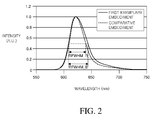
- FIG. 2 is a graph illustrating a full width at half maximum (FWHM) of a main peak wavelength of red light according to a first exemplary embodiment and a comparative embodiment of the present disclosure.
- a horizontal axis of the graph represents a wavelength and a vertical axis represents an intensity of the light.
- a unit of the horizontal axis is nm and A.U. (arbitrary unit) which is a unit of the vertical axis is a value obtained by normalizing an intensity of light by 1.
- the FWHM is a numerical value representing a width of a wavelength when an intensity of light becomes half. As the FWHM is increased, a light emitting spectrum becomes broader, so that the color shift depending on a viewing angle may be suppressed.
- the optical multilayer film is formed of one inorganic insulating layer.
- the optical multilayer film includes four optical layers having different thicknesses and four organic layers are alternatively disposed in the order of an optical layer having a high refractive index and an organic layer having a low refractive index.
- a last optical layer is formed to be thick in order to secure the reliability of the organic light emitting element.
- the capping layer, the optical multilayer film, the organic layer, and the passivation layer represented in Table 1 are deposited on the organic light emitting element in this order.
- a full width at half maximum of a main peak wavelength (RFWHM_E) of the red light according to the first exemplary embodiment of the present disclosure is 35.2 nm, which is 4.9 nm broader than a full width at half maximum of a main peak wavelength (RFWHM_R) of the red light according to the comparative embodiment which is 30.3 nm.
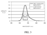
- a full width at half maximum of a main peak wavelength (GFWHM_E) of the green light according to the first exemplary embodiment of the present disclosure is 30.7 nm, which is 5.4 nm broader than a full width at half maximum of a main peak wavelength (GFWHM_R) of the green light according to the comparative embodiment which is 25.3 nm.
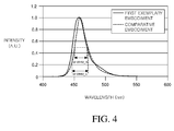
- a full width at half maximum of a main peak wavelength (BFWHM_E) of the blue light according to the first exemplary embodiment of the present disclosure is 23.6 nm, which is 2.6 nm broader than a full width at half maximum of a main peak wavelength (BFWHM_R) of the blue light according to the comparative embodiment which is 21 nm.
- the full width at half maximum of a main peak wavelength of each of the red light, the green light, and the blue light emitted from the organic light emitting display element according to the first exemplary embodiment in which the optical multilayer film including a plurality of optical layers is disposed is larger than the full width at half maximum of a main peak wavelength of each of the red light, the green light, and the blue light emitted from the organic light emitting display element according to the comparative embodiment in which the single layer is disposed on the organic light emitting element. That is, the reflected light generated at the interface of the optical layer having a small refractive index and the optical layer having a large refractive index causes interference in the optical multilayer film, to generate the weak microcavity effect. Therefore, the full width at half maximum of a main peak wavelength may be increased as compared with a structure in which the optical multilayer film is not used. Therefore, the color shift depending on a viewing angle is reduced and the efficiency of the organic light emitting element may be improved.
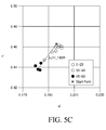
- FIGS. 5A to 5D are graphs illustrating a color coordinate shift amount of white light depending on a viewing angle in right, upper, left, and lower directions from a center of the organic light emitting display device as comparative embodiments and FIGS. 6A to 6D are graphs illustrating a color coordinate shift amount of white light depending on a viewing angle in right, upper, left, and lower directions from a center of the organic light emitting display device as a first exemplary embodiment.
- the right, upper, left, and lower directions of the organic light emitting display device may be represented by azimuth angles of 0°, 90°, 180°, and 270°.
- the color coordinate shift amount ( ⁇ u'v') refers to a difference of a color coordinate as seen at the front and a color coordinate at a viewing angle and the color coordinate (u'v') refers to 1976 UCS color space defined in International Commission on Illumination CIE 15.2.
- the viewing angle measured in FIGS. 5A to 5D are 0° to 60° and a viewing angle at a start position X is 0°.
- the graphs of FIGS. 5A to 5D are results obtained by applying a structure of the comparative embodiment listed in Table 1.
- the maximum color coordinate shift amount ( ⁇ u'v'_0R) is approximately 0.016.
- the maximum color coordinate shift amount ( ⁇ u'v'_90R) is approximately 0.018.
- the maximum color coordinate shift amount ( ⁇ u'v'_180R) is approximately 0.029.
- the maximum color coordinate shift amount ( ⁇ u'v'_270R) is approximately 0.015.
- the graphs of FIGS. 6A to 6D are results obtained by applying a structure of the first exemplary embodiment listed in Table 1.
- the maximum color coordinate shift amount ( ⁇ u'v'_0E) is approximately 0.013.
- the maximum color coordinate shift amount ( ⁇ u'v'_90E) is approximately 0.012.
- the maximum color coordinate shift amount ( ⁇ u'v'_180E) is approximately 0.012.
- the maximum color coordinate shift amount ( ⁇ u'v'_270E) is approximately 0.006.
- the maximum color coordinate shift amount of the first exemplary embodiment is smaller than that of the comparative embodiment. That is, the maximum color coordinate shift amount of the white light emitted from the organic light emitting display device according to the comparative embodiment in which the optical multilayer film is formed by a single layer is larger than the maximum color coordinate shift amount of the white light emitted from the organic light emitting display device according to the first exemplary embodiment in which the optical multilayer film including a plurality of optical layers having a high refractive index and optical layers having a low refractive index. Therefore, when the first exemplary embodiment is applied, the color shift depending on a viewing angle is reduced and the efficiency of the organic light emitting element is improved.
- FIG. 7 is a cross-sectional view illustrating an organic light emitting display device according to a second exemplary embodiment of the present disclosure.
- the organic light emitting display device according to the second exemplary embodiment may include the same components as those of the first exemplary embodiment described above and redundant description with the first exemplary embodiment will be omitted.
- FIG. 7 illustrates a structure in which an organic layer 141 and a passivation layer 142 are added to the structure of the first exemplary embodiment.
- the passivation layer 142 which protects the organic light emitting element 100 is added to the structure of the first exemplary embodiment, so that the thickness of the fourth optical layer 124 may be smaller than the thickness applied in the first exemplary embodiment and the fourth optical layer 124 may be omitted.
- the passivation layer 142 is disposed on the optical multilayer film 120 to suppress moisture and oxygen from permeating into the organic light emitting element 100 and improve the reliability of the organic light emitting element 100.
- the passivation layer 142 is an inorganic insulating layer and is formed of any one or more of silicon nitride SiNx, silicon oxide SiOx, and silicon oxynitride SiON, but is not limited thereto.
- a thickness of the passivation layer 142 may be between 0.05 ⁇ m and 1.5 ⁇ m, but is not limited thereto.
- the organic layer 141 is an organic insulating layer which may be disposed between the optical multilayer film 120 and the passivation layer 142 and may be formed of polymer.
- the organic layer 141 is also referred to as a particle covering layer (PCL) and servers to cover the particles.
- PCL particle covering layer
- the passivation layer 142 which is formed of an inorganic insulating material is disposed on the optical multilayer film 120 with particles attached on the surface thereof, without having the organic layer 141, the inorganic insulating material does not have strong adhesion with the particles attached on the surface of the optical multilayer film 120, so that there may be gaps around the particles. Therefore, the passivation layer 142 may be separated therefrom due to the formation of the gap.
- the organic layer 141 which is formed of an organic material is disposed between the optical multilayer film 120 and the passivation layer 142 to cover the particles and the surroundings of the particles to suppress the passivation layer 142 from being separated.
- the thickness of the organic layer 141 may be between 5 ⁇ m and 20 ⁇ m, but is not limited thereto.
- FIG. 8 is a cross-sectional view illustrating an organic light emitting display device according to a third exemplary embodiment of the present disclosure.
- the organic light emitting display device according to the third exemplary embodiment may include the same components as those of the first exemplary embodiment described above and redundant description with the first exemplary embodiment will be omitted.
- FIG. 8 illustrates a structure in which an atomic deposition layer 150 is added to the structure of the first exemplary embodiment.
- the atomic deposition layer 150 is disposed between the capping layer 110 and the optical multilayer film 120 and may be formed of any one or more of silicon oxide SiOx and aluminum oxide Al 2 O 3 , but is not limited thereto.
- the atomic deposition layer 150 is a layer formed using an atomic layer deposition (ALD) technique.
- the atomic deposition layer is formed by accumulating atomic layers so that very thin film may be formed and a thickness and a composition of the film may be precisely controlled. Therefore, the film may be uniformly formed even on a large size substrate and a stack coverage ability is excellent so that a surface of the capping layer 110 is covered by the atomic deposition layer 150, to improve the reliability of the organic light emitting element 100.
- FIG. 9 is a cross-sectional view illustrating an organic light emitting display device according to a fourth exemplary embodiment of the present disclosure.
- the organic light emitting display device according to the fourth exemplary embodiment may include the same components as those of the first and third exemplary embodiments described above and redundant description with the first and third exemplary embodiments will be omitted.
- FIG. 9 illustrates a structure in which the atomic deposition layer 150 described with reference to FIG. 8 is disposed on the optical multilayer film 120.
- the atomic deposition layer 150 is located at the top of the organic light emitting display device 1000 to closely seal not only the organic light emitting element 100 but also the optical multilayer film 120 using the excellent stack coverage ability, to improve the reliability of the organic light emitting display device 1000.
- the atomic deposition layer 150 is formed to be in contact with the optical multilayer film 120 to secure the reliability of the organic light emitting display device 1000.
- the passivation layer is further disposed on the optical multilayer film 120 or the atomic deposition layer 150 to further improve the reliability of the organic light emitting display device 1000.
- an organic light emitting display device includes an organic light emitting element including a cathode, an anode, and an organic light emitting layer; and an optical multilayer film on the organic light emitting element.
- the optical multilayer film is constructed such that a full width at half maximum of light emitted from the organic light emitting element is larger than a full width at half maximum of light emitted from a structure in which the optical multilayer film is not used, thereby reducing color shift depending on a viewing angle of the organic light emitting display device and improving efficiency of the organic light emitting element.
- the organic light emitting display device may further include a passivation layer on the optical multilayer film.
- the organic light emitting display device may further include an organic layer between the optical multilayer film and the passivation layer.
- the optical multilayer film may include three optical layers having different refractive indexes.
- the three optical layers may be formed such that a first optical layer, a second optical layer, and a third optical layer are sequentially deposited on the cathode and a refractive index of the second optical layer is smaller than those of the first optical layer and the third optical layer.
- the optical multilayer film may include four optical layers and refractive indexes of odd-numbered deposited optical layers from the cathode may be larger than those of even-numbered deposited optical layers.
- a thickness of the last deposited optical layer among the four optical layers may be between 100 nm and 5000 nm.
- the organic light emitting display device may further include an insulating layer on the organic light emitting element and a thickness of the insulating layer may be less than 5 nm.
- the optical multilayer film may include a plurality of optical layers and an optical layer having a relatively small refractive index among the plurality of optical layers may be formed of silicon oxynitride (SiON).
- the organic light emitting display device may further include an atomic deposition layer above or below the optical multilayer film.
- an organic light emitting display device includes an organic light emitting element including a cathode, an anode, and an organic light emitting layer; and an optical multilayer film including a plurality of optical layers on the organic light emitting element.
- the optical multilayer film may be configured to cause a weak microcavity effect. Therefore, a full width at half maximum (FWHM) of a main peak wavelength of the light emitted from the organic light emitting element is larger than that of the case when the single optical layer is used, thereby reducing color shift depending on a viewing angle of the organic light emitting display device and improving efficiency of the organic light emitting element.
- FWHM full width at half maximum
- the optical multilayer film may include a pair of optical layers in which an optical layer having a relatively larger refractive index and an optical layer having a relatively smaller refractive index are sequentially disposed.
- the optical multilayer film may further include another pair of optical layers in which an optical layer having a relatively larger refractive index and an optical layer having a relatively smaller refractive index are sequentially disposed.
- a difference of the refractive indexes of the optical layer having a relatively larger refractive index and the optical layer having a relatively smaller refractive index may be between 0.01 and 0.6.
- the organic light emitting display device may further include a functional layer on the organic light emitting layer and configured to reduce separation due to a difference of expansion coefficients of the optical multilayer film and the organic light emitting layer.
- the organic light emitting display device may further include an atomic deposition layer which is contact with an upper portion or a lower portion of the optical multilayer film.
- an organic light emitting display device includes: an organic light emitting element including a cathode and an optical multilayer film deposited a first optical layer and a second optical layer in order on the organic light emitting element.
- a refractive index of the first optical layer is larger than a refractive index of the second optical layer. Therefore, in addition to primary interference, secondary interference is generated in the optical multilayer film to reduce the color shift depending on a viewing angle and improve efficiency of the organic light emitting element.
- the refractive index of the first optical layer may be larger than a refractive index of the cathode.
- the optical multilayer film may further include a third optical layer and the refractive index of the second optical layer may be smaller than a refractive index of the third optical layer.
- the optical multilayer film may further include a fourth optical layer and the refractive index of the third optical layer may be larger than a refractive index of the fourth optical layer.
Landscapes
- Physics & Mathematics (AREA)
- Optics & Photonics (AREA)
- Engineering & Computer Science (AREA)
- Microelectronics & Electronic Packaging (AREA)
- Electroluminescent Light Sources (AREA)
- Geometry (AREA)
Abstract
Description
- This application claims the priority of Korean Patent Application No.
10-2016-0081206 filed on June 28, 2016 - The present disclosure relates to an organic light emitting display device which disposes an optical multilayer film on an organic light emitting element to reduce color shift depending on a viewing angle and improve efficiency of the organic light emitting device.
- An active organic light emitting display device includes an organic light emitting element including an organic light emitting layer, an anode, and a cathode and a driving circuit (for example, a transistor or a capacitor) which drives the organic light emitting element. Specifically, the organic light emitting display device is a display apparatus in which holes and electrons injected from an anode and a cathode are recombined to each other in a light emitting layer to form an exciton and light having a specific wavelength is generated by emitting energy of the exciton. Therefore, the organic light emitting display device uses a self-light emitting organic light emitting element so as to have a high response speed, a high contrast ratio, a high luminous efficiency, a high brightness, and a wide viewing angle.
- In this case, optical efficiency of the organic light emitting display device is divided into an internal efficiency and an external efficiency. The internal efficiency depends on photoelectric conversion efficiency of an organic light emitting material. The external efficiency is also referred to as light coupling efficiency and depends on refractive indexes of each layers constituting the organic light emitting element. In this case, the light coupling efficiency of the organic light emitting display device is lower than those of other display devices. This is because when light discharged from the organic light emitting layer is emitted at a critical angle or larger, for example, total reflection is caused at an interface between a layer having a high refractive index such as an electrode formed of indium tin oxide (ITO) which forms an anode or a cathode and a layer having a low refractive index such as an encapsulating layer. Therefore, the light is suppressed from being extracted to the outside. Accordingly, approximately 20% of light substantially emitted from the organic light emitting element in the organic light emitting display device is extracted to the outside.
- As described above, the self-emitted light from the organic light emitting device goes out of the organic light emitting display device through various components of the organic light emitting display device. However, some light of light emitted from the organic light emitting layer does not go out from the organic light emitting display device but is locked in the organic light emitting display device. That is, there is an interface having different refractive indexes on an emission surface of the organic light emitting element so that reflection, absorption, scattering, refraction, and the like, are generated, which may lower the light coupling efficiency. Therefore, the light coupling efficiency at a front surface and a side surface of the organic light emitting display device may be considered as a problem.
- In order to solve the problem of the light coupling efficiency, a method which varies a thickness and a refractive index of the organic light emitting layers disposed on the organic light emitting element or adds an organic layer to cause strong microcavity effect in the organic light emitting element, thereby increasing efficiency of the light may be used. Here, the strong microcavity refers to a state in which intensity of light is increased by reducing a full width at half maximum of a main peak wavelength. However, when the thickness and the refractive index of the organic light emitting layer vary or an organic layer is added to the organic light emitting layer, the microcavity effect becomes strong so that a color of emitted light changes depending on a viewing angle and the emitted light has straightness. Therefore, the light may not have Lambertian distribution. Therefore, when the strong microcavity is used, front light efficiency and color purity are improved. However, light efficiency at a viewing angle may be reduced and color shift may be significant.
- Inventors of the present disclosure invented an organic light emitting display device which forms an optical multilayer film serving as an optical cavity on a light emitting surface of an organic light emitting display device to reduce color shift depending on a viewing angle and improve efficiency of an organic light emitting element.
- An object to be achieved by an exemplary embodiment of the present disclosure is to provide an organic light emitting display device which optimizes a deposition order of optical layers which form an optical multilayer film in accordance with refractive indexes to allow light which is primarily interfered in the organic light emitting elment to be incident onto the optical multilayer film to cause secondary interference in the optical multilayer film to generate weak microcavity effect and increase a full width at half maximum (FWHM) of a main peak wavelength of the light. That is, the weak microcavity refers to a state when the FWHM of the main peak wavelength is increased to less affect the property of the viewing angle. Therefore, a structure which generates the weak microcavity effect is applied to reduce the color shift depending on a viewing angle.
- Another object to be achieved by an exemplary embodiment of the present disclosure is to provide an organic light emitting display device which optimizes the number and the thickness of optical layers which form the optical multilayer film, to solve a reliability problem of the organic light emitting display device which is in a trade-off relationship with a method for reducing the color shift depending on a viewing angle.
- Objects of the present disclosure are not limited to the above-mentioned objects, and other objects, which are not mentioned above, can be clearly understood by those skilled in the art from the following descriptions.
- According to an aspect of the present disclosure, there is provided an organic light emitting display device. The organic light emitting display device includes an organic light emitting element including a cathode, an anode, and an organic light emitting layer, and an optical multilayer film on the organic light emitting element. Herein, the optical multilayer film is formed such that a full width at half maximum of light emitted from the organic light emitting element is larger than a full width at half maximum of light emitted from a structure in which the optical multilayer film is not used. Therefore, the color shift depending on a viewing angle of the organic light emitting display device may be reduced and efficiency of the organic light emitting element may be improved.
- According to an aspect of the present disclosure, there is provided an organic light emitting display device. The organic light emitting display device includes an organic light emitting element including a cathode, an anode, and an organic light emitting layer, and an optical multilayer film on the organic light emitting element. Herein, the optical multilayer film is formed to have a structure which generates weak microcavity effect, thereby reducing the color shift depending on a viewing angle of the organic light emitting display device and improving efficiency of the organic light emitting element.
- According to an aspect of the present disclosure, there is provided an organic light emitting display device. The organic light emitting display device includes an organic light emitting element including a cathode, and an optical multilayer film are deposited a first optical layer and a second optical layer in order on the organic light emitting element. A refractive index of the first optical layer is larger than a refractive index of the second optical layer so that the color shift depending on a viewing angle of the organic light emitting display device may be reduced and efficiency of the organic light emitting element may be improved.
- Other detailed matters of the embodiments are included in the detailed description and the drawings.
- According to the exemplary embodiments of the present disclosure, the optical multilayer film is disposed on the organic light emitting element so that the optical multilayer film is formed such that a full width at half maximum of light emitted from the organic light emitting element is larger than a full width at half maximum of light emitted from a structure in which the optical multilayer film is not used. Therefore, the color shift depending on a viewing angle may be reduced and efficiency of the organic light emitting element may be improved.
- According to the exemplary embodiments of the present disclosure, the capping layer is formed to have a thickness of less than 5 nm. Therefore, the color shift depending on a viewing angle is reduced and the optical multilayer film is suppressed from being separated from the organic light emitting element.
- Further, according to the exemplary embodiments of the present disclosure, the refractive index of the first optical layer is larger than the refractive index of the cathode and the third optical layer having a refractive index which is larger than that of the second optical layer is disposed on the second optical layer. Therefore, the light which passes through the organic light emitting element causes secondary interference, to reduce the color shift depending on a viewing angle and improve the efficiency of the organic light emitting element.
- According to the exemplary embodiments of the present disclosure, a fourth optical layer is additionally formed and the fourth optical layer may be formed to have a thickness which is between 100 nm and 5000 nm. Therefore, the reliability of the organic light emitting element may be maintained without additionally providing a passivation layer on the optical multilayer film.
- Therefore, according to the exemplary embodiments of the present disclosure, the optical layers having small refractive indexes among the optical layers which configure the optical multilayer film are formed of silicon oxynitride SiON, to suppress hydrogen H2 from being generated when the optical layer is formed, thereby suppressing the deterioration of the organic light emitting layer.
- Further, according to the exemplary embodiments of the present disclosure, the organic layer and the passivation layer are formed on the optical multilayer film to suppress the optical multilayer film from being separated due to particles which are formed on the optical multilayer film and improve the reliability of the organic light emitting device.
- Further, according to the exemplary embodiments of the present disclosure, the atomic deposition layer is formed on the optical multilayer film to closely cover the stack of the optical multilayer film, thereby improving the reliability of the organic light emitting element.
- Further, according to the exemplary embodiments of the present disclosure, the atomic deposition layer is formed on the capping layer to cover a surface of the capping layer, thereby improving the reliability of the organic light emitting element.
- Furthermore, according to the exemplary embodiments of the present disclosure, the difference in refractive indexes of optical layers which form the optical multilayer film is between 0.01 and 0.06. Therefore, the optical layer may be suppressed from being separated due to the difference in expansion coefficients depending on the difference in the refraction indexes of the optical layers during the evaluation of reliability.
- Further, according to the exemplary embodiments of the present disclosure, a structure in which the optical multilayer film causes weak microcavity effect is applied to reduce the color shift depending on a viewing angle and improve the efficiency of the organic light emitting element.
- The objects to be achieved by the present disclosure, the means for achieving the objects, and effects of the present disclosure described above do not specify essential features of the claims, and, thus, the scope of the claims is not limited to the disclosure of the present disclosure.
- The above and other aspects, features and other advantages of the present disclosure will be more clearly understood from the following detailed description taken in conjunction with the accompanying drawings, in which:
-
FIG. 1 is a cross-sectional view illustrating an organic light emitting display device according to a first exemplary embodiment of the present disclosure; -
FIG. 2 is a graph illustrating a full width at half maximum of a main peak wavelength of red light according to a first exemplary embodiment and a comparative embodiment of the present disclosure; -
FIG. 3 is a graph illustrating a full width at half maximum of a main peak wavelength of green light according to a first exemplary embodiment and a comparative embodiment of the present disclosure; -
FIG. 4 is a graph illustrating a full width at half maximum of a main peak wavelength of blue light according to a first exemplary embodiment and a comparative embodiment of the present disclosure; -
FIGS. 5A to 5D are graphs illustrating a color coordinate shift amount of white light depending on a viewing angle in right, upper, left, and lower directions from a center of the organic light emitting display device as a comparative embodiment; -
FIGS. 6A to 6D are graphs illustrating a color coordinate shift amount of white light depending on a viewing angle in right, upper, left, and lower directions from a center of the organic light emitting display device as a first exemplary embodiment; -
FIG. 7 is a cross-sectional view illustrating an organic light emitting display device according to a second exemplary embodiment of the present disclosure; -
FIG. 8 is a cross-sectional view illustrating an organic light emitting display device according to a third exemplary embodiment of the present disclosure; and -
FIG. 9 is a cross-sectional view illustrating an organic light emitting display device according to a fourth exemplary embodiment of the present disclosure. - Advantages and characteristics of the present disclosure and a method of achieving the advantages and characteristics will be clear by referring to exemplary embodiments described below in detail together with the accompanying drawings. However, the present disclosure is not limited to exemplary embodiment disclosed herein but will be implemented in various forms. The exemplary embodiments are provided by way of example only so that a person of ordinary skilled in the art can fully understand the disclosures of the present disclosure and the scope of the present disclosure. Therefore, the present disclosure will be defined only by the scope of the appended claims.
- The shapes, sizes, ratios, angles, numbers, and the like illustrated in the accompanying drawings for describing the exemplary embodiments of the present disclosure are merely examples, and the present disclosure is not limited thereto. Like reference numerals generally denote like elements throughout the specification. Further, in the following description, a detailed explanation of known related technologies may be omitted to avoid unnecessarily obscuring the subject matter of the present disclosure. The terms such as "including," "having," and "consist of" used herein are generally intended to allow other components to be added unless the terms are used with the term "only". Any references to singular may include plural unless expressly stated otherwise.
- Components are interpreted to include an ordinary error range even if not expressly stated.
- When the position relation between two parts is described using the terms such as "on", "above", "below", and "next", one or more parts may be positioned between the two parts unless the terms are used with the term "immediately" or "directly" is not used.
- When the relation of a time sequential order is described using the terms such as "after", "continuously to", "next to", and "before", the order may not be continuous unless the terms are used with the term "immediately" or "directly".
- Although the terms "first", "second", and the like are used for describing various components, these components are not confined by these terms. These terms are merely used for distinguishing one component from the other components. Therefore, a first component to be mentioned below may be a second component in a technical concept of the present disclosure.
- The features of various embodiments of the present disclosure can be partially or entirely bonded to or combined with each other and can be interlocked and operated in technically various ways, and the embodiments can be carried out independently of or in association with each other.
- Hereinafter, an organic light emitting display device according to an exemplary embodiment of the present disclosure will be described with reference to the accompanying drawings.
-
FIG. 1 is a cross-sectional view illustrating an organic light emitting display device according to a first exemplary embodiment of the present disclosure. - An organic light emitting
display device 1000 includes asubstrate 104, an organiclight emitting element 100, acapping layer 110, and anoptical multilayer film 120 which are disposed on thesubstrate 104. - A driving circuit which drives the organic
light emitting element 100 may be disposed on thesubstrate 104 and include a transistor and a capacitor. In this case, the driving circuit may be formed corresponding to a plurality of sub pixels formed on thesubstrate 104 and is connected to ananode 101 of the organiclight emitting element 100. - The
substrate 104 may be formed of an insulating material. For example, thesubstrate 104 may be formed of a glass or a flexible film formed of a polyimide, acryl, polyacrylate, polycarbonate, polyether, sulfonic acid based material, silicon oxide (SiOx), or the like, but is not limited thereto. - The organic
light emitting element 100 disposed on thesubstrate 104 includes ananode 101, an organiclight emitting layer 102, and acathode 103. In this case, a hole injecting layer and a hole transporting layer may be included between the organiclight emitting layer 102 and theanode 101 and an electron transporting layer and an electron injecting layer may be included between the organiclight emitting layer 102 and thecathode 103. However, the present disclosure is not limited thereto. Further, the organiclight emitting layer 102 may be a single layer structure having one light emitting layer as a light emitting layer which emits red light, blue light, green light or similar color light. Alternatively, the organiclight emitting layer 102 may have a tandem structure in which two or more light emitting layers are provided and a charge generating layer (CGL) is included between the light emitting layers. - The light emitted from the organic
light emitting layer 102 causes primary interference between theanode 101 and thecathode 103. Specifically, the organiclight emitting element 100 may have a structure and a thickness determined by considering a microcavity distance between theanode 101 and thecathode 103 depending on a wavelength of light emitted from the organiclight emitting layer 102. The microcavity refers that light emitted from the light emitting layer is amplified by being repeatedly reflected and re-reflected between theanode 101 and thecathode 103 to cause constructive interference, thereby improving luminous efficiency. In this case, the organiclight emitting layer 102 may be formed to be separated in every sub pixel and a distance between theanode 101 and thecathode 103 may vary depending on a color of light emitted from every sub pixel. In the meantime, in the organic light emitting display device using white light, the organiclight emitting layer 102 may be commonly formed in a plurality of sub pixels. - As described above, the
anode 101 may be disposed to be separated for every sub pixel and is connected to a source electrode or a drain electrode of a transistor which is disposed on thesubstrate 104, as an electrode which supplies or delivers the hole to the organiclight emitting layer 102. - In a top emission type organic light emitting
display device 1000, a plurality ofanodes 101 may include a reflective layer so that the light emitted from the organiclight emitting layer 102 is reflected from theanode 101 to be smoothly discharged to an upward direction (or a direction which passes through the cathode 103). For example, theanode 101 may have a dual layered structure in which a transparent layer and the reflective layer are laminated or a triple layered structure in which a transparent layer, a reflective layer and a transparent layer are laminated. The transparent layer may be formed of a transparent conductive oxide such as indium tin oxide (ITO) or indium zinc oxide (IZO). The reflective layer may be formed of a metal material such as copper (Cu), silver (Ag), palladium (Pd), aluminum (Al), platinum (Pt), gold (Au), chrome (Cr), tungsten (W), molybdenum (Mo), titanium (Ti), or iridium (Ir). Alternatively, theanode 101 may be a single layer configured by a material or a structure having characteristics of a transparent layer and a reflective layer. - The
cathode 103 is commonly disposed for a plurality of sub pixels and supplies and delivers the electron to the organiclight emitting layer 102. - In the top emission type organic light emitting
display device 1000, thecathode 103 may be transparent so that light emitted from the organiclight emitting layer 102 passes through the cathode. For example, thecathode 103 may be disposed by forming a metal material such as silver (Ag), magnesium (Mg), or an alloy thoseof to have a very small thickness. Alternatively, thecathode 103 may be formed of a transparent conductive oxide material such as indium tin oxide or indium zinc oxide, similarly to the transparent layer of theanode 101. - The light emitted from the organic
light emitting element 100 due to theprimary interference 131 has a strong microcavity effect, that is, an effect of improving the luminous efficiency. However, as the intensity of light is increased by the strong microcavity effect, there may be a problem in that a viewing angle characteristic of the organic light emittingdisplay device 1000 is lowered. Here, the strong microcavity refers to a state in which intensity of light is increased by reducing a full width at half maximum of a main peak wavelength. Specifically, according to the strong microcavity effect, as the intensity of the light emitted from the organiclight emitting element 100 is increased, the full width at half maximum of a main peak wavelength of light is reduced. Therefore, the front efficiency of the organic light emittingdisplay device 1000 is increased but the viewing angle characteristic is lowered. Therefore, in order to reduce the color shift depending on a viewing angle and increase the efficiency of the organiclight emitting element 100 by increasing the full width at half maximum of a main peak wavelength of light while maintaining the intensity of the light of the organic light emittingdisplay device 1000, in the organic light emittingdisplay device 1000 according to the first exemplary embodiment, anoptical multilayer film 120 may be provided on a surface onto which light emitted from the organiclight emitting element 100 is emitted. Theoptical multilayer film 120 will be described below and thecapping layer 110 will be described now. - The
capping layer 110 may be disposed between the organiclight emitting element 100 and theoptical multilayer film 120. Thecapping layer 110 covers the organiclight emitting element 100 to block inflow of oxygen and moisture entering from the outside and improve the efficiency of the light which passes through thecathode 103. However, when thecapping layer 110 is formed to have a large thickness, for example, approximately 40 nm, to improve the reliability of the organiclight emitting element 100, the color shift may be significantly caused depending on a viewing angle of the light emitted from the organic light emittingdisplay device 1000. In contrast, when thecapping layer 110 is removed to remove the color shift depending on a viewing angle, which is generated by thecapping layer 110, theoptical multilayer film 120 may be undesirably separated from the organiclight emitting element 100 at the time of evaluating the reliability of the organic light emittingdisplay device 1000. - Generally, after completing a product, reliability evaluation is performed to evaluate reliability of the product. The reliability evaluation is evaluation to check deformation of an appearance of the product when the product is left in a chamber in high temperature/high humidity environment, for example, 50°C/90% or 60°C/80% for several hours or several tens of hours or a problem of a screen at the time of driving. By performing the reliability evaluation, products which withstand the high temperature/high humidity environment may be shipped. The temperature or humidity for reliability evaluation is an exemplary embodiment, but does not limit the contents of the present disclosure.
- That is, when the reliability of the organic light emitting
display device 1000 which does not have thecapping layer 110 is evaluated, since an expansion coefficient of the organiclight emitting layer 102 which is formed of an organic material is different from an expansion coefficient of theoptical multilayer film 120 which is formed of an inorganic material in the high temperature/high humidity environment, a gap is formed between the organiclight emitting element 100 including the organiclight emitting layer 102 and theoptical multilayer film 120 so that the organiclight emitting element 100 and theoptical multilayer film 120 are separated from each other. Therefore, thecapping layer 110 is disposed between the organiclight emitting element 100 and theoptical multilayer film 120 so that theoptical multilayer film 120 is adhered to the organiclight emitting element 100. In this case, thecapping layer 110 is a functional layer which is formed to be thin so as to hardly apply an optical effect. A thickness of thecapping layer 110 may be less than 5 nm. Thecapping layer 110 may be an insulating layer which is formed of an organic material or an inorganic material. Therefore, thecapping layer 110 may suppress theoptical multilayer film 120 from being separated from the organiclight emitting element 100. - The
optical multilayer film 120 which is adhered to the organiclight emitting element 100 by thecapping layer 110 includes a plurality of optical layers. A firstoptical layer 121, a secondoptical layer 122, a thirdoptical layer 123, and a fourthoptical layer 124 may be sequentially disposed. - An arrow of
FIG. 1 represents a route of the light which is emitted to the front side from the organiclight emitting layer 102 and representsprimary interference 131 which is optical interference generated in the organiclight emitting element 100 due to reflection of the light generated at an interface of the organiclight emitting layer 102 and theanode 101 and thecathode 103 in the organiclight emitting element 100 andsecondary interference 132 due to the reflection of the light generated at an interface of optical layers having different refractive indexes in theoptical multilayer film 120. - The first
optical layer 121 may be formed to have a refractive index which is larger than a refractive index of thecathode 103. The light emitted through thecathode 103 is reflected (132A) at the interface of the firstoptical layer 121 having a refractive index which is larger than that of thecathode 103 and thecathode 103. Secondary interference of the light 132A which is reflected at the interface of the firstoptical layer 121 and thecathode 103 is generated in theoptical multilayer film 120. In this case, an optical influence which is applied to the light emitted through thecathode 103 by thecapping layer 110 disposed between the firstoptical layer 121 and thecathode 103 may be so small to be ignored. - When light having an incident angle of zero (vertical to an incident surface) is incident from a material having a small refractive index to a material having a large refractive index, reflected light is generated at an interface between the material having a small refractive index and the material having a large refractive index. An amount of the reflected light generated in this case is larger than an amount of reflected light generated when light having an incident angle of zero is incident from a material having a large refractive index to a material having a small refractive index. Therefore, the light is caused to be incident from a material having a small refractive index to a material having a large refractive index, so that the amount of the reflected light is increased and the secondary interference by the reflected light is efficiently generated.
- Next, the second
optical layer 122 is disposed on the firstoptical layer 121. The secondoptical layer 122 may be formed to have a refractive index which is smaller than that of the firstoptical layer 121. - Further, the third
optical layer 123 is disposed on the secondoptical layer 122. The thirdoptical layer 123 may be formed to have a refractive index which is larger than that of the secondoptical layer 122. Therefore, the light emitted through the secondoptical layer 122 is reflected (132B) at the interface of the thirdoptical layer 123 having a refractive index which is larger than that of the secondoptical layer 122 and the secondoptical layer 122. Secondary interference of the light 132B which is reflected at the interface of the thirdoptical layer 123 and the secondoptical layer 122 is generated in theoptical multilayer film 120. - Therefore, the secondary interference of the light which is reflected at the interface of the
cathode 103 and the firstoptical layer 121 and the interface of the secondoptical layer 122 and the thirdoptical layer 123 is generated in theoptical multilayer film 120 so that the organic light emittingdisplay device 1000 according to the first exemplary embodiment generates weak microcavity effect as compared with a case when nooptical multilayer film 120 is disposed or a single layer is disposed. Therefore, the color shift depending on a viewing angle is reduced by increasing a full width at half maximum of a main peak wavelength of red, green, and blue and thus the efficiency of the organic light emitting device is improved. Here, the weak microcavity refers to a state when the FWHM of the main peak wavelength is increased to less affect the property of the viewing angle. - Next, the fourth
optical layer 124 may be disposed on the thirdoptical layer 123. The fourthoptical layer 124 may be formed to have a refractive index which is smaller than that of the thirdoptical layer 123 and the light which passes through the thirdoptical layer 123 is emitted through the fourthoptical layer 124. In this case, the fourthoptical layer 124 may be formed to have a thickness between 100 nm and 5000 nm, to improve the reliability of the organiclight emitting element 100. Further, when no passivation layer is disposed on the fourthoptical layer 124, the thickness of the fourthoptical layer 124 may be formed to be thicker than the fourthoptical layer 124 on which the passivation layer is disposed. However, the present disclosure is not limited thereto. - In this case, when the difference of refractive indexes of the first
optical layer 121 and the secondoptical layer 122, the difference of refractive indexes of the secondoptical layer 122 and the thirdoptical layer 123, and the difference of refractive indexes of the thirdoptical layer 123 and the fourthoptical layer 124 are large, the separation may be generated due to the difference of expansion coefficients between optical layers having a large difference in refractive indexes during the reliability evaluation. Therefore, the optical layers may be formed to have the difference in refractive indexes of less than 0.6 at least 0.01. - The optical multilayer film which is formed of the above-described first to fourth
optical layers optical layers display device 1000 may be reduced. However, when several optical layers are added, even though the color shift depending on a viewing angle is reduced, there may be another problem in that another characteristic of the organic light emittingdisplay device 1000, for example, front efficiency or brightness is lowered. Therefore, it is important to optimize the number of optical layers to achieve the effect of the present disclosure without causing the problems related with the efficiency, the brightness, or the like. - That is, the
optical multilayer film 120 which is formed of three or four optical layers may be effective due to the following reasons. When a white screen is displayed on the organic light emittingdisplay device 1000, the white screen does not have yellow color and the separation of the optical multilayer film due to the difference of refractive indexes is suppressed during the reliability evaluation. Further, as the number of optical layers is increased, a possibility of haze of the optical multilayer film is increased, which may affect the brightness of the display device. The smaller the number of optical layers, the lower the possibility of haze. Further, the smaller the number of optical layers, the shorter the time to clean an optical layer deposition chamber. Therefore, the processing time may be shortened. - Therefore, according to the present disclosure, the minimum number of optical layers is used, so that the amount of light reflected due to the difference in refractive indexes of the optical layers is generated at maximum, so that the light which passes through the organic
light emitting element 100 causes the secondary interference. - The
optical multilayer film 120 may be formed of any one or more of silicon nitride SiNx, silicon oxide SiOx, and silicon oxynitride SiON. Among these, refractive indexes of silicon oxide SiOx and silicon oxynitride SiON are approximately between 1.46 and 1.5 at a wavelength of 400 nm to 700 nm and a refractive index of silicon nitride SiNx is approximately between 1.9 and 2.3. Therefore, the refractive indexes of silicon oxide SiOx and silicon oxynitride SiON are smaller than that of silicon nitride SiNx. Further, oxygen atom included in silicon oxide SiOx and silicon oxynitride SiON is coupled to hydrogen H2 which is generated when an optical layer is formed so that hydrogen H2 is suppressed from permeating into the organiclight emitting element 100 to deteriorate the organiclight emitting element 100. - Therefore, the optical layers having small refractive indexes among the optical layers which configure the
optical multilayer film 120 are formed of silicon oxide SiOx or silicon oxynitride SiON, to suppress hydrogen H2 from being generated when the optical layer is formed, thereby suppressing the deterioration of the organic light emitting layer. For example, the secondoptical layer 122 which is adjacent to the firstoptical layer 121 and has a small refractive index and the fourthoptical layer 124 which is adjacent to the thirdoptical layer 123 and has a small refractive index may be formed of silicon oxide SiOx or silicon oxynitride SiON. -
FIG. 2 is a graph illustrating a full width at half maximum (FWHM) of a main peak wavelength of red light according to a first exemplary embodiment and a comparative embodiment of the present disclosure. A horizontal axis of the graph represents a wavelength and a vertical axis represents an intensity of the light. A unit of the horizontal axis is nm and A.U. (arbitrary unit) which is a unit of the vertical axis is a value obtained by normalizing an intensity of light by 1. In this case, the FWHM is a numerical value representing a width of a wavelength when an intensity of light becomes half. As the FWHM is increased, a light emitting spectrum becomes broader, so that the color shift depending on a viewing angle may be suppressed. - Conditions of a layer which is disposed on the organic light emitting element according to the first exemplary embodiment and the comparative embodiment of
FIGS. 2 to 4 are represented in the following Table 1.[Table 1] Capping layer Optical multilayer film Organic layer Passivation layer Comp. Ex. Is provided? ○ SiNx ○ ○ Thickness 40 nm 1.5 µm 18 µm 1.5 µm First Ex. Is provided? ○ SiNx SiNx SiNx SiNx X X Thickness 5 nm 500 nm 200 nm 300 nm 900 nm - - - According to the comparative embodiment, in the organic light emitting display device formed as represented in Table 1, the optical multilayer film is formed of one inorganic insulating layer. According to the first exemplary embodiment, the optical multilayer film includes four optical layers having different thicknesses and four organic layers are alternatively disposed in the order of an optical layer having a high refractive index and an organic layer having a low refractive index. In the first exemplary embodiment in which the organic layer and the passivation layer are not provided, a last optical layer is formed to be thick in order to secure the reliability of the organic light emitting element. The capping layer, the optical multilayer film, the organic layer, and the passivation layer represented in Table 1 are deposited on the organic light emitting element in this order.
- Referring to
FIG. 2 , a full width at half maximum of a main peak wavelength (RFWHM_E) of the red light according to the first exemplary embodiment of the present disclosure is 35.2 nm, which is 4.9 nm broader than a full width at half maximum of a main peak wavelength (RFWHM_R) of the red light according to the comparative embodiment which is 30.3 nm. - Referring to
FIG. 3 , a full width at half maximum of a main peak wavelength (GFWHM_E) of the green light according to the first exemplary embodiment of the present disclosure is 30.7 nm, which is 5.4 nm broader than a full width at half maximum of a main peak wavelength (GFWHM_R) of the green light according to the comparative embodiment which is 25.3 nm. - Referring to
FIG. 4 , a full width at half maximum of a main peak wavelength (BFWHM_E) of the blue light according to the first exemplary embodiment of the present disclosure is 23.6 nm, which is 2.6 nm broader than a full width at half maximum of a main peak wavelength (BFWHM_R) of the blue light according to the comparative embodiment which is 21 nm. - Referring to
FIGS. 2 to 4 , the full width at half maximum of a main peak wavelength of each of the red light, the green light, and the blue light emitted from the organic light emitting display element according to the first exemplary embodiment in which the optical multilayer film including a plurality of optical layers is disposed is larger than the full width at half maximum of a main peak wavelength of each of the red light, the green light, and the blue light emitted from the organic light emitting display element according to the comparative embodiment in which the single layer is disposed on the organic light emitting element. That is, the reflected light generated at the interface of the optical layer having a small refractive index and the optical layer having a large refractive index causes interference in the optical multilayer film, to generate the weak microcavity effect. Therefore, the full width at half maximum of a main peak wavelength may be increased as compared with a structure in which the optical multilayer film is not used. Therefore, the color shift depending on a viewing angle is reduced and the efficiency of the organic light emitting element may be improved. -
FIGS. 5A to 5D are graphs illustrating a color coordinate shift amount of white light depending on a viewing angle in right, upper, left, and lower directions from a center of the organic light emitting display device as comparative embodiments andFIGS. 6A to 6D are graphs illustrating a color coordinate shift amount of white light depending on a viewing angle in right, upper, left, and lower directions from a center of the organic light emitting display device as a first exemplary embodiment. In this case, the right, upper, left, and lower directions of the organic light emitting display device may be represented by azimuth angles of 0°, 90°, 180°, and 270°. The color coordinate shift amount (Δu'v') refers to a difference of a color coordinate as seen at the front and a color coordinate at a viewing angle and the color coordinate (u'v') refers to 1976 UCS color space defined in International Commission on Illumination CIE 15.2. The viewing angle measured inFIGS. 5A to 5D are 0° to 60° and a viewing angle at a start position X is 0°. - The graphs of
FIGS. 5A to 5D are results obtained by applying a structure of the comparative embodiment listed in Table 1. - Referring to
FIG. 5A , in a graph obtained by forming a viewing angle to the right direction (azimuth angle is 0°) in a state when the front is seen at the center of the organic light emitting display device to measure the color coordinate of the white light, the maximum color coordinate shift amount (Δu'v'_0R) is approximately 0.016. - Referring to
FIG. 5B , in a graph obtained by forming a viewing angle to the upper direction (azimuth angle is 90°) in a state when the front is seen at the center of the organic light emitting display device to measure the color coordinate of the white light, the maximum color coordinate shift amount (Δu'v'_90R) is approximately 0.018. - Referring to
FIG. 5C , in a graph obtained by forming a viewing angle to the left direction (azimuth angle is 180°) in a state when the front is seen at the center of the organic light emitting display device to measure the color coordinate of the white light, the maximum color coordinate shift amount (Δu'v'_180R) is approximately 0.029. - Referring to
FIG. 5D , in a graph obtained by forming a viewing angle to the lower direction (azimuth angle is 270°) in a state when the front is seen at the center of the organic light emitting display device to measure the color coordinate of the white light, the maximum color coordinate shift amount (Δu'v'_270R) is approximately 0.015. - The graphs of
FIGS. 6A to 6D are results obtained by applying a structure of the first exemplary embodiment listed in Table 1. - Referring to
FIG. 6A , in a graph obtained by forming a viewing angle to the right direction (azimuth angle is 0°) in a state when the front is seen at the center of the organic light emitting display device to measure the color coordinate of the white light, the maximum color coordinate shift amount (Δu'v'_0E) is approximately 0.013. - Referring to
FIG. 6B , in a graph obtained by forming a viewing angle to the upper direction (azimuth angle is 90°) in a state when the front is seen at the center of the organic light emitting display device to measure the color coordinate of the white light, the maximum color coordinate shift amount (Δu'v'_90E) is approximately 0.012. - Referring to
FIG. 6C , in a graph obtained by forming a viewing angle to the left direction (azimuth angle is 180°) in a state when the front is seen at the center of the organic light emitting display device to measure the color coordinate of the white light, the maximum color coordinate shift amount (Δu'v'_180E) is approximately 0.012. - Referring to
FIG. 6D , in a graph obtained by forming a viewing angle to the lower direction (azimuth angle is 270°) in a state when the front is seen at the center of the organic light emitting display device to measure the color coordinate of the white light, the maximum color coordinate shift amount (Δu'v'_270E) is approximately 0.006. - When the maximum color coordinate shift amounts of the comparative embodiment and the first exemplary embodiment are compared according to the direction of forming a viewing angle, it is confirmed that the maximum color coordinate shift amount of the first exemplary embodiment is smaller than that of the comparative embodiment. That is, the maximum color coordinate shift amount of the white light emitted from the organic light emitting display device according to the comparative embodiment in which the optical multilayer film is formed by a single layer is larger than the maximum color coordinate shift amount of the white light emitted from the organic light emitting display device according to the first exemplary embodiment in which the optical multilayer film including a plurality of optical layers having a high refractive index and optical layers having a low refractive index. Therefore, when the first exemplary embodiment is applied, the color shift depending on a viewing angle is reduced and the efficiency of the organic light emitting element is improved.
-
FIG. 7 is a cross-sectional view illustrating an organic light emitting display device according to a second exemplary embodiment of the present disclosure. The organic light emitting display device according to the second exemplary embodiment may include the same components as those of the first exemplary embodiment described above and redundant description with the first exemplary embodiment will be omitted. -
FIG. 7 illustrates a structure in which anorganic layer 141 and apassivation layer 142 are added to the structure of the first exemplary embodiment. Thepassivation layer 142 which protects the organiclight emitting element 100 is added to the structure of the first exemplary embodiment, so that the thickness of the fourthoptical layer 124 may be smaller than the thickness applied in the first exemplary embodiment and the fourthoptical layer 124 may be omitted. - The
passivation layer 142 is disposed on theoptical multilayer film 120 to suppress moisture and oxygen from permeating into the organiclight emitting element 100 and improve the reliability of the organiclight emitting element 100. Thepassivation layer 142 is an inorganic insulating layer and is formed of any one or more of silicon nitride SiNx, silicon oxide SiOx, and silicon oxynitride SiON, but is not limited thereto. A thickness of thepassivation layer 142 may be between 0.05 µm and 1.5 µm, but is not limited thereto. - The
organic layer 141 is an organic insulating layer which may be disposed between theoptical multilayer film 120 and thepassivation layer 142 and may be formed of polymer. Theorganic layer 141 is also referred to as a particle covering layer (PCL) and servers to cover the particles. For example, when thepassivation layer 142 which is formed of an inorganic insulating material is disposed on theoptical multilayer film 120 with particles attached on the surface thereof, without having theorganic layer 141, the inorganic insulating material does not have strong adhesion with the particles attached on the surface of theoptical multilayer film 120, so that there may be gaps around the particles. Therefore, thepassivation layer 142 may be separated therefrom due to the formation of the gap. Therefore, theorganic layer 141 which is formed of an organic material is disposed between theoptical multilayer film 120 and thepassivation layer 142 to cover the particles and the surroundings of the particles to suppress thepassivation layer 142 from being separated. In this case, the thickness of theorganic layer 141 may be between 5 µm and 20 µm, but is not limited thereto. -
FIG. 8 is a cross-sectional view illustrating an organic light emitting display device according to a third exemplary embodiment of the present disclosure. The organic light emitting display device according to the third exemplary embodiment may include the same components as those of the first exemplary embodiment described above and redundant description with the first exemplary embodiment will be omitted. -
FIG. 8 illustrates a structure in which anatomic deposition layer 150 is added to the structure of the first exemplary embodiment. Theatomic deposition layer 150 is disposed between thecapping layer 110 and theoptical multilayer film 120 and may be formed of any one or more of silicon oxide SiOx and aluminum oxide Al2O3, but is not limited thereto. - The
atomic deposition layer 150 is a layer formed using an atomic layer deposition (ALD) technique. The atomic deposition layer is formed by accumulating atomic layers so that very thin film may be formed and a thickness and a composition of the film may be precisely controlled. Therefore, the film may be uniformly formed even on a large size substrate and a stack coverage ability is excellent so that a surface of thecapping layer 110 is covered by theatomic deposition layer 150, to improve the reliability of the organiclight emitting element 100. -
FIG. 9 is a cross-sectional view illustrating an organic light emitting display device according to a fourth exemplary embodiment of the present disclosure. The organic light emitting display device according to the fourth exemplary embodiment may include the same components as those of the first and third exemplary embodiments described above and redundant description with the first and third exemplary embodiments will be omitted. -
FIG. 9 illustrates a structure in which theatomic deposition layer 150 described with reference toFIG. 8 is disposed on theoptical multilayer film 120. As illustrated inFIG. 9 , theatomic deposition layer 150 is located at the top of the organic light emittingdisplay device 1000 to closely seal not only the organiclight emitting element 100 but also theoptical multilayer film 120 using the excellent stack coverage ability, to improve the reliability of the organic light emittingdisplay device 1000. - In
FIG. 8 or9 , theatomic deposition layer 150 is formed to be in contact with theoptical multilayer film 120 to secure the reliability of the organic light emittingdisplay device 1000. The passivation layer is further disposed on theoptical multilayer film 120 or theatomic deposition layer 150 to further improve the reliability of the organic light emittingdisplay device 1000. - The exemplary embodiments of the present disclosure can also be described as follows:
- According to an aspect of the present disclosure, an organic light emitting display device includes an organic light emitting element including a cathode, an anode, and an organic light emitting layer; and an optical multilayer film on the organic light emitting element. Herein, the optical multilayer film is constructed such that a full width at half maximum of light emitted from the organic light emitting element is larger than a full width at half maximum of light emitted from a structure in which the optical multilayer film is not used, thereby reducing color shift depending on a viewing angle of the organic light emitting display device and improving efficiency of the organic light emitting element.
- The organic light emitting display device may further include a passivation layer on the optical multilayer film.
- The organic light emitting display device may further include an organic layer between the optical multilayer film and the passivation layer.
- The optical multilayer film may include three optical layers having different refractive indexes.
- The three optical layers may be formed such that a first optical layer, a second optical layer, and a third optical layer are sequentially deposited on the cathode and a refractive index of the second optical layer is smaller than those of the first optical layer and the third optical layer.
- The optical multilayer film may include four optical layers and refractive indexes of odd-numbered deposited optical layers from the cathode may be larger than those of even-numbered deposited optical layers.
- A thickness of the last deposited optical layer among the four optical layers may be between 100 nm and 5000 nm.
- The organic light emitting display device may further include an insulating layer on the organic light emitting element and a thickness of the insulating layer may be less than 5 nm.
- The optical multilayer film may include a plurality of optical layers and an optical layer having a relatively small refractive index among the plurality of optical layers may be formed of silicon oxynitride (SiON).
- The organic light emitting display device may further include an atomic deposition layer above or below the optical multilayer film.
- According to another aspect of the present disclosure, an organic light emitting display device includes an organic light emitting element including a cathode, an anode, and an organic light emitting layer; and an optical multilayer film including a plurality of optical layers on the organic light emitting element. The optical multilayer film may be configured to cause a weak microcavity effect. Therefore, a full width at half maximum (FWHM) of a main peak wavelength of the light emitted from the organic light emitting element is larger than that of the case when the single optical layer is used, thereby reducing color shift depending on a viewing angle of the organic light emitting display device and improving efficiency of the organic light emitting element.
- The optical multilayer film may include a pair of optical layers in which an optical layer having a relatively larger refractive index and an optical layer having a relatively smaller refractive index are sequentially disposed.
- The optical multilayer film may further include another pair of optical layers in which an optical layer having a relatively larger refractive index and an optical layer having a relatively smaller refractive index are sequentially disposed.
- A difference of the refractive indexes of the optical layer having a relatively larger refractive index and the optical layer having a relatively smaller refractive index may be between 0.01 and 0.6.
- The organic light emitting display device may further include a functional layer on the organic light emitting layer and configured to reduce separation due to a difference of expansion coefficients of the optical multilayer film and the organic light emitting layer.
- The organic light emitting display device may further include an atomic deposition layer which is contact with an upper portion or a lower portion of the optical multilayer film.
- According to yet another aspect of the present disclosure, an organic light emitting display device includes: an organic light emitting element including a cathode and an optical multilayer film deposited a first optical layer and a second optical layer in order on the organic light emitting element. Herein, a refractive index of the first optical layer is larger than a refractive index of the second optical layer. Therefore, in addition to primary interference, secondary interference is generated in the optical multilayer film to reduce the color shift depending on a viewing angle and improve efficiency of the organic light emitting element.
- The refractive index of the first optical layer may be larger than a refractive index of the cathode.
- The optical multilayer film may further include a third optical layer and the refractive index of the second optical layer may be smaller than a refractive index of the third optical layer.
- The optical multilayer film may further include a fourth optical layer and the refractive index of the third optical layer may be larger than a refractive index of the fourth optical layer.
Claims (15)
- An organic light emitting display device (1000), comprising:an organic light emitting element (100) including a cathode (103), an anode (101), and an organic light emitting layer (102); andan optical multilayer film (120) on the organic light emitting element (100),wherein the optical multilayer film (120) is constructed such that a full width at half maximum of light emitted from the organic light emitting element (100) is larger than a full width at half maximum of light emitted from a structure in which the optical multilayer film (120) is not used.
- The organic light emitting display device (1000) according to claim 1, further comprising:a passivation layer (142) on the optical multilayer film (120).
- The organic light emitting display device (1000) according to claim 2, further comprising:an organic layer (141) between the optical multilayer film (120) and the passivation layer (142).
- The organic light emitting display device (1000) according to claim 2 or 3, wherein the optical multilayer film (120) includes three optical layers (121, 122, 123) having different refractive indexes.
- The organic light emitting display device (1000) according to claim 4, wherein the three optical layers (121, 122, 123) are deposited as a first optical layer (121), a second optical layer (122), and a third optical layer (123) in order on the cathode (103) and a refractive index of the second optical layer (122) is smaller than those of the first optical layer (121) and the third optical layer (123).
- The organic light emitting display device (1000) according to any one of claims 1 to 3, wherein the optical multilayer film (120) includes four optical layers (121, 122, 123, 124) and refractive indexes of odd-numbered deposited optical layers (121, 123) from the cathode (103) among the four optical layers (121, 122, 123, 124) are larger than those of even-numbered deposited optical layers (122, 124).
- The organic light emitting display device (1000) according to claim 6, wherein a thickness of the last deposited optical layer (124) among the four optical layers (121, 122, 123, 124) is between 100 nm and 5000 nm.
- The organic light emitting display device (1000) according to any one of claims 1 to 7, further comprising:an insulating layer (110) on the organic light emitting element (100), andwherein a thickness of the insulating layer (110) is less than 5 nm.
- The organic light emitting display device (1000) according to any one of claims 1 to 8, wherein the optical multilayer film (120) includes a plurality of optical layers (121, 122, 123, 124) and an optical layer having a relatively small refractive index among the plurality of optical layers (121, 122, 123, 124) is formed of silicon oxynitride.
- The organic light emitting display device (1000) according to any one of claims 1 to 9, further comprising:an atomic deposition layer (150) above or below the optical multilayer film (120).
- The organic light emitting display device (1000) according to any one of claims 1 to 3,
wherein the optical multilayer film (120) is configured to cause a weak microcavity effect. - The organic light emitting display device (1000) according to claim 11, wherein the optical multilayer film (120) includes a pair of optical layers (121, 122) in which an optical layer (121) having a relatively larger refractive index and an optical layer (122) having a relatively smaller refractive index are sequentially disposed,
wherein, preferably, the optical multilayer film (120) further includes another pair of optical layers (123, 124) in which an optical layer (123) having a relatively larger refractive index and an optical layer (124) having a relatively smaller refractive index are sequentially disposed. - The organic light emitting display device (1000) according to claim 12, wherein a difference of the refractive indexes of the optical layer (121, 123) having a relatively larger refractive index and the optical layer (122, 124) having a relatively smaller refractive index is between 0.01 and 0.6.
- The organic light emitting display device (1000) according to any one of claims 11 to 13, further comprising:a functional layer (110) on the organic light emitting layer (102) and configured to reduce separation due to a difference of expansion coefficients of the optical multilayer film (120) and the organic light emitting layer (102).
- The organic light emitting display device (1000) according to any one of claims 11 to 14, further comprising:an atomic deposition layer (150) which is contact with an upper portion or a lower portion of the optical multilayer film (120).
Priority Applications (1)
| Application Number | Priority Date | Filing Date | Title |
|---|---|---|---|
| EP23188374.5A EP4243590A3 (en) | 2016-06-28 | 2016-09-30 | Organic light emitting display device |
Applications Claiming Priority (1)
| Application Number | Priority Date | Filing Date | Title |
|---|---|---|---|
| KR1020160081206A KR102631878B1 (en) | 2016-06-28 | 2016-06-28 | Organic light emitting display device |
Related Child Applications (2)
| Application Number | Title | Priority Date | Filing Date |
|---|---|---|---|
| EP23188374.5A Division-Into EP4243590A3 (en) | 2016-06-28 | 2016-09-30 | Organic light emitting display device |
| EP23188374.5A Division EP4243590A3 (en) | 2016-06-28 | 2016-09-30 | Organic light emitting display device |
Publications (2)
| Publication Number | Publication Date |
|---|---|
| EP3264483A1 true EP3264483A1 (en) | 2018-01-03 |
| EP3264483B1 EP3264483B1 (en) | 2023-09-06 |
Family
ID=57047085
Family Applications (2)
| Application Number | Title | Priority Date | Filing Date |
|---|---|---|---|
| EP16191755.4A Active EP3264483B1 (en) | 2016-06-28 | 2016-09-30 | Organic light emitting display device |
| EP23188374.5A Pending EP4243590A3 (en) | 2016-06-28 | 2016-09-30 | Organic light emitting display device |
Family Applications After (1)
| Application Number | Title | Priority Date | Filing Date |
|---|---|---|---|
| EP23188374.5A Pending EP4243590A3 (en) | 2016-06-28 | 2016-09-30 | Organic light emitting display device |
Country Status (4)
| Country | Link |
|---|---|
| US (1) | US10644265B2 (en) |
| EP (2) | EP3264483B1 (en) |
| KR (3) | KR102631878B1 (en) |
| CN (1) | CN107546333B (en) |
Families Citing this family (15)
| Publication number | Priority date | Publication date | Assignee | Title |
|---|---|---|---|---|
| JP2018139262A (en) * | 2017-02-24 | 2018-09-06 | 株式会社Joled | Organic EL display element, organic EL display panel, and method for manufacturing organic EL display element |
| KR102391617B1 (en) * | 2017-12-29 | 2022-04-27 | 엘지디스플레이 주식회사 | Flexible organic light emitting display device |
| US10367162B1 (en) | 2018-03-28 | 2019-07-30 | Sharp Kabushiki Kaisha | Light-emitting device including optical cavity with low angular colour shift |
| US11003287B2 (en) * | 2018-03-30 | 2021-05-11 | Sharp Kabushiki Kaisha | Touch sensor for display with improved viewing angle uniformity |
| CN110473974B (en) * | 2018-05-11 | 2021-12-24 | 株式会社日本有机雷特显示器 | Light emitting device |
| JP2019197694A (en) * | 2018-05-11 | 2019-11-14 | 株式会社ジャパンディスプレイ | Display |
| KR102749542B1 (en) * | 2019-02-19 | 2025-01-02 | 삼성디스플레이 주식회사 | Display device |
| CN109830516B (en) | 2019-02-22 | 2021-11-12 | 京东方科技集团股份有限公司 | OLED substrate and display device |
| CN110970572B (en) * | 2019-11-14 | 2025-06-17 | 京东方科技集团股份有限公司 | Packaging structure, display panel and display device |
| KR102855884B1 (en) * | 2020-03-30 | 2025-09-05 | 삼성디스플레이 주식회사 | Display device |
| CN114695779B (en) * | 2020-12-25 | 2025-06-27 | 京东方科技集团股份有限公司 | Display panel and display device thereof |
| KR102541927B1 (en) | 2021-02-01 | 2023-06-13 | 삼성디스플레이 주식회사 | Display device |
| CN114975815A (en) * | 2021-02-25 | 2022-08-30 | 京东方科技集团股份有限公司 | Display panel, preparation method thereof, display device and vehicle |
| CN113193150B (en) * | 2021-04-28 | 2023-06-16 | 合肥京东方卓印科技有限公司 | Top light-emitting display panel and display device |
| WO2025249693A1 (en) * | 2024-05-29 | 2025-12-04 | 포항공과대학교 산학협력단 | High-efficiency light-emitting display device |
Citations (4)
| Publication number | Priority date | Publication date | Assignee | Title |
|---|---|---|---|---|
| US20060250084A1 (en) * | 2005-05-04 | 2006-11-09 | Eastman Kodak Company | OLED device with improved light output |
| US20100243999A1 (en) * | 2007-08-31 | 2010-09-30 | Tokyo Electron Limited | Organic electronic device, organic electronic device manufacturing method, organic electronic device manufacturing apparatus, substrate processing system, protection film structure and storage medium with control program stored therein |
| US20110100458A1 (en) * | 2009-11-05 | 2011-05-05 | Korea Institute Of Machinery And Materials | Multi-layer thin film for encapsulation and method thereof |
| WO2014041743A1 (en) * | 2012-09-11 | 2014-03-20 | Sony Corporation | Display unit, method of manufacturing the same, and electronic apparatus |
Family Cites Families (18)
| Publication number | Priority date | Publication date | Assignee | Title |
|---|---|---|---|---|
| US5405710A (en) * | 1993-11-22 | 1995-04-11 | At&T Corp. | Article comprising microcavity light sources |
| US5478658A (en) * | 1994-05-20 | 1995-12-26 | At&T Corp. | Article comprising a microcavity light source |
| CN100477329C (en) * | 2003-03-07 | 2009-04-08 | 友达光电股份有限公司 | Preparation method of organic light emitting display |
| US6917159B2 (en) * | 2003-08-14 | 2005-07-12 | Eastman Kodak Company | Microcavity OLED device |
| GB2447637B (en) * | 2004-08-04 | 2009-11-18 | Cambridge Display Tech Ltd | Organic Electroluminescent Device |
| US20060066220A1 (en) * | 2004-09-27 | 2006-03-30 | Choong Vi-En | Reduction or elimination of color change with viewing angle for microcavity devices |
| US20090015141A1 (en) * | 2004-12-30 | 2009-01-15 | E.I. Du Pont De Nemours And Company | Electronic Device Having An Optical Resonator |
| US20100051973A1 (en) * | 2008-08-28 | 2010-03-04 | Seiko Epson Corporation | Light-emitting device, electronic equipment, and process of producing light-emitting device |
| JP5333757B2 (en) * | 2009-06-23 | 2013-11-06 | セイコーエプソン株式会社 | Light emitting device |
| KR101182447B1 (en) * | 2010-06-16 | 2012-09-12 | 삼성디스플레이 주식회사 | Organic light emitting device and manufacturing method thereof |
| JP2012247705A (en) | 2011-05-30 | 2012-12-13 | Seiko Epson Corp | Polarization conversion element, polarization conversion unit, and projection type video device |
| US9891361B2 (en) * | 2011-08-05 | 2018-02-13 | Lg Display Co., Ltd. | Organic light emitting display device and method of manufacturing the same |
| KR101970567B1 (en) * | 2012-12-14 | 2019-04-19 | 엘지디스플레이 주식회사 | Organic light emitting display panel |
| EP2983224B1 (en) * | 2013-09-30 | 2020-08-26 | LG Display Co., Ltd. | Organic electronic device |
| EP4583637A3 (en) * | 2014-09-30 | 2025-09-03 | LG Display Co., Ltd. | Flexible organic light emitting display device |
| KR20160083986A (en) * | 2015-01-02 | 2016-07-13 | 삼성디스플레이 주식회사 | Organic light emitting diode device |
| KR102417119B1 (en) * | 2015-02-11 | 2022-07-06 | 삼성디스플레이 주식회사 | Flexible display device |
| KR102407115B1 (en) * | 2015-06-25 | 2022-06-09 | 삼성디스플레이 주식회사 | Organic light emitting diode display |
-
2016
- 2016-06-28 KR KR1020160081206A patent/KR102631878B1/en active Active
- 2016-09-30 EP EP16191755.4A patent/EP3264483B1/en active Active
- 2016-09-30 CN CN201610875991.7A patent/CN107546333B/en active Active
- 2016-09-30 EP EP23188374.5A patent/EP4243590A3/en active Pending
- 2016-10-12 US US15/291,349 patent/US10644265B2/en active Active
-
2024
- 2024-01-26 KR KR1020240012405A patent/KR102934612B1/en active Active
- 2024-01-26 KR KR1020240012404A patent/KR20240016392A/en active Pending
Patent Citations (4)
| Publication number | Priority date | Publication date | Assignee | Title |
|---|---|---|---|---|
| US20060250084A1 (en) * | 2005-05-04 | 2006-11-09 | Eastman Kodak Company | OLED device with improved light output |
| US20100243999A1 (en) * | 2007-08-31 | 2010-09-30 | Tokyo Electron Limited | Organic electronic device, organic electronic device manufacturing method, organic electronic device manufacturing apparatus, substrate processing system, protection film structure and storage medium with control program stored therein |
| US20110100458A1 (en) * | 2009-11-05 | 2011-05-05 | Korea Institute Of Machinery And Materials | Multi-layer thin film for encapsulation and method thereof |
| WO2014041743A1 (en) * | 2012-09-11 | 2014-03-20 | Sony Corporation | Display unit, method of manufacturing the same, and electronic apparatus |
Also Published As
| Publication number | Publication date |
|---|---|
| US10644265B2 (en) | 2020-05-05 |
| KR102934612B1 (en) | 2026-03-05 |
| KR20240017875A (en) | 2024-02-08 |
| KR20240016392A (en) | 2024-02-06 |
| EP3264483B1 (en) | 2023-09-06 |
| EP4243590A2 (en) | 2023-09-13 |
| EP4243590A3 (en) | 2023-11-29 |
| KR102631878B1 (en) | 2024-01-30 |
| US20170373277A1 (en) | 2017-12-28 |
| KR20180001982A (en) | 2018-01-05 |
| CN107546333A (en) | 2018-01-05 |
| CN107546333B (en) | 2020-04-14 |
Similar Documents
| Publication | Publication Date | Title |
|---|---|---|
| EP3264483B1 (en) | Organic light emitting display device | |
| US20250107327A1 (en) | Optoelectronic device including a light transmissive region | |
| JP5425242B2 (en) | ORGANIC EL ELEMENT AND DISPLAY DEVICE USING THE SAME | |
| US7187121B2 (en) | Organic luminescence device with anti-reflection layer and organic luminescence device package | |
| US10516130B2 (en) | Light emitting apparatus with optical interference layer having a larger refractive index than a light emitting layer | |
| US10431773B2 (en) | Organic light emitting display device | |
| US8987716B2 (en) | Organic light-emitting diode (OLED) display device and method of manufacturing the same | |
| KR102605614B1 (en) | Organic light emitting display device | |
| CN1607876A (en) | Organic light emitting device, manufacturing method thereof, and display unit | |
| EP3573106B1 (en) | Display device and image pickup apparatus | |
| US8183564B2 (en) | Multicolor display apparatus | |
| KR20150131522A (en) | Organic light emitting diode display panel | |
| US20090298209A1 (en) | Optoelectronic device manufacturing | |
| JP2013118173A (en) | Display device | |
| CN102598865A (en) | Organic electroluminescent element and display including same | |
| US20180151840A1 (en) | Light emission device, display apparatus, and illumination apparatus | |
| KR20200002673A (en) | Display device | |
| KR20190074037A (en) | Organic light emitting display device | |
| KR102317267B1 (en) | Organic light emitting diode | |
| US12114554B2 (en) | Light-emitting device including complementary color light absorption layer | |
| KR20200081194A (en) | Display device | |
| KR20200080742A (en) | Display device | |
| EP4565042A1 (en) | Light emitting diode and display device using the same |
Legal Events
| Date | Code | Title | Description |
|---|---|---|---|
| PUAI | Public reference made under article 153(3) epc to a published international application that has entered the european phase |
Free format text: ORIGINAL CODE: 0009012 |
|
| STAA | Information on the status of an ep patent application or granted ep patent |
Free format text: STATUS: REQUEST FOR EXAMINATION WAS MADE |
|
| 17P | Request for examination filed |
Effective date: 20160930 |
|
| AK | Designated contracting states |
Kind code of ref document: A1 Designated state(s): AL AT BE BG CH CY CZ DE DK EE ES FI FR GB GR HR HU IE IS IT LI LT LU LV MC MK MT NL NO PL PT RO RS SE SI SK SM TR |
|
| AX | Request for extension of the european patent |
Extension state: BA ME |
|
| RBV | Designated contracting states (corrected) |
Designated state(s): AL AT BE BG CH CY CZ DE DK EE ES FI FR GB GR HR HU IE IS IT LI LT LU LV MC MK MT NL NO PL PT RO RS SE SI SK SM TR |
|
| STAA | Information on the status of an ep patent application or granted ep patent |
Free format text: STATUS: EXAMINATION IS IN PROGRESS |
|
| 17Q | First examination report despatched |
Effective date: 20200217 |
|
| REG | Reference to a national code |
Ref country code: DE Ref legal event code: R079 Free format text: PREVIOUS MAIN CLASS: H01L0051520000 Ipc: H10K0050844000 Ref country code: DE Ref legal event code: R079 Ref document number: 602016082488 Country of ref document: DE Free format text: PREVIOUS MAIN CLASS: H01L0051520000 Ipc: H10K0050844000 |
|
| GRAP | Despatch of communication of intention to grant a patent |
Free format text: ORIGINAL CODE: EPIDOSNIGR1 |
|
| STAA | Information on the status of an ep patent application or granted ep patent |
Free format text: STATUS: GRANT OF PATENT IS INTENDED |
|
| RIC1 | Information provided on ipc code assigned before grant |
Ipc: H10K 50/858 20230101ALI20230222BHEP Ipc: H10K 50/852 20230101ALI20230222BHEP Ipc: H10K 50/844 20230101AFI20230222BHEP |
|
| INTG | Intention to grant announced |
Effective date: 20230329 |
|
| RIN1 | Information on inventor provided before grant (corrected) |
Inventor name: RYU, DAEWON Inventor name: LEE, SANGHO Inventor name: LIM, YOUNGNAM Inventor name: NOH, SEONGHEE |
|
| GRAS | Grant fee paid |
Free format text: ORIGINAL CODE: EPIDOSNIGR3 |
|
| GRAA | (expected) grant |
Free format text: ORIGINAL CODE: 0009210 |
|
| STAA | Information on the status of an ep patent application or granted ep patent |
Free format text: STATUS: THE PATENT HAS BEEN GRANTED |
|
| AK | Designated contracting states |
Kind code of ref document: B1 Designated state(s): AL AT BE BG CH CY CZ DE DK EE ES FI FR GB GR HR HU IE IS IT LI LT LU LV MC MK MT NL NO PL PT RO RS SE SI SK SM TR |
|
| REG | Reference to a national code |
Ref country code: GB Ref legal event code: FG4D |
|
| REG | Reference to a national code |
Ref country code: CH Ref legal event code: EP |
|
| REG | Reference to a national code |
Ref country code: DE Ref legal event code: R096 Ref document number: 602016082488 Country of ref document: DE |
|
| REG | Reference to a national code |
Ref country code: IE Ref legal event code: FG4D |
|
| REG | Reference to a national code |
Ref country code: LT Ref legal event code: MG9D |
|
| REG | Reference to a national code |
Ref country code: NL Ref legal event code: MP Effective date: 20230906 |
|
| PG25 | Lapsed in a contracting state [announced via postgrant information from national office to epo] |
Ref country code: GR Free format text: LAPSE BECAUSE OF FAILURE TO SUBMIT A TRANSLATION OF THE DESCRIPTION OR TO PAY THE FEE WITHIN THE PRESCRIBED TIME-LIMIT Effective date: 20231207 |
|
| PG25 | Lapsed in a contracting state [announced via postgrant information from national office to epo] |
Ref country code: SE Free format text: LAPSE BECAUSE OF FAILURE TO SUBMIT A TRANSLATION OF THE DESCRIPTION OR TO PAY THE FEE WITHIN THE PRESCRIBED TIME-LIMIT Effective date: 20230906 Ref country code: RS Free format text: LAPSE BECAUSE OF FAILURE TO SUBMIT A TRANSLATION OF THE DESCRIPTION OR TO PAY THE FEE WITHIN THE PRESCRIBED TIME-LIMIT Effective date: 20230906 Ref country code: NO Free format text: LAPSE BECAUSE OF FAILURE TO SUBMIT A TRANSLATION OF THE DESCRIPTION OR TO PAY THE FEE WITHIN THE PRESCRIBED TIME-LIMIT Effective date: 20231206 Ref country code: LV Free format text: LAPSE BECAUSE OF FAILURE TO SUBMIT A TRANSLATION OF THE DESCRIPTION OR TO PAY THE FEE WITHIN THE PRESCRIBED TIME-LIMIT Effective date: 20230906 Ref country code: LT Free format text: LAPSE BECAUSE OF FAILURE TO SUBMIT A TRANSLATION OF THE DESCRIPTION OR TO PAY THE FEE WITHIN THE PRESCRIBED TIME-LIMIT Effective date: 20230906 Ref country code: HR Free format text: LAPSE BECAUSE OF FAILURE TO SUBMIT A TRANSLATION OF THE DESCRIPTION OR TO PAY THE FEE WITHIN THE PRESCRIBED TIME-LIMIT Effective date: 20230906 Ref country code: GR Free format text: LAPSE BECAUSE OF FAILURE TO SUBMIT A TRANSLATION OF THE DESCRIPTION OR TO PAY THE FEE WITHIN THE PRESCRIBED TIME-LIMIT Effective date: 20231207 Ref country code: FI Free format text: LAPSE BECAUSE OF FAILURE TO SUBMIT A TRANSLATION OF THE DESCRIPTION OR TO PAY THE FEE WITHIN THE PRESCRIBED TIME-LIMIT Effective date: 20230906 |
|
| REG | Reference to a national code |
Ref country code: AT Ref legal event code: MK05 Ref document number: 1610294 Country of ref document: AT Kind code of ref document: T Effective date: 20230906 |
|
| PG25 | Lapsed in a contracting state [announced via postgrant information from national office to epo] |
Ref country code: NL Free format text: LAPSE BECAUSE OF FAILURE TO SUBMIT A TRANSLATION OF THE DESCRIPTION OR TO PAY THE FEE WITHIN THE PRESCRIBED TIME-LIMIT Effective date: 20230906 |
|
| PG25 | Lapsed in a contracting state [announced via postgrant information from national office to epo] |
Ref country code: IS Free format text: LAPSE BECAUSE OF FAILURE TO SUBMIT A TRANSLATION OF THE DESCRIPTION OR TO PAY THE FEE WITHIN THE PRESCRIBED TIME-LIMIT Effective date: 20240106 |
|
| PG25 | Lapsed in a contracting state [announced via postgrant information from national office to epo] |
Ref country code: AT Free format text: LAPSE BECAUSE OF FAILURE TO SUBMIT A TRANSLATION OF THE DESCRIPTION OR TO PAY THE FEE WITHIN THE PRESCRIBED TIME-LIMIT Effective date: 20230906 |
|
| PG25 | Lapsed in a contracting state [announced via postgrant information from national office to epo] |
Ref country code: ES Free format text: LAPSE BECAUSE OF FAILURE TO SUBMIT A TRANSLATION OF THE DESCRIPTION OR TO PAY THE FEE WITHIN THE PRESCRIBED TIME-LIMIT Effective date: 20230906 |
|
| PG25 | Lapsed in a contracting state [announced via postgrant information from national office to epo] |
Ref country code: SM Free format text: LAPSE BECAUSE OF FAILURE TO SUBMIT A TRANSLATION OF THE DESCRIPTION OR TO PAY THE FEE WITHIN THE PRESCRIBED TIME-LIMIT Effective date: 20230906 Ref country code: RO Free format text: LAPSE BECAUSE OF FAILURE TO SUBMIT A TRANSLATION OF THE DESCRIPTION OR TO PAY THE FEE WITHIN THE PRESCRIBED TIME-LIMIT Effective date: 20230906 Ref country code: IS Free format text: LAPSE BECAUSE OF FAILURE TO SUBMIT A TRANSLATION OF THE DESCRIPTION OR TO PAY THE FEE WITHIN THE PRESCRIBED TIME-LIMIT Effective date: 20240106 Ref country code: ES Free format text: LAPSE BECAUSE OF FAILURE TO SUBMIT A TRANSLATION OF THE DESCRIPTION OR TO PAY THE FEE WITHIN THE PRESCRIBED TIME-LIMIT Effective date: 20230906 Ref country code: EE Free format text: LAPSE BECAUSE OF FAILURE TO SUBMIT A TRANSLATION OF THE DESCRIPTION OR TO PAY THE FEE WITHIN THE PRESCRIBED TIME-LIMIT Effective date: 20230906 Ref country code: CZ Free format text: LAPSE BECAUSE OF FAILURE TO SUBMIT A TRANSLATION OF THE DESCRIPTION OR TO PAY THE FEE WITHIN THE PRESCRIBED TIME-LIMIT Effective date: 20230906 Ref country code: AT Free format text: LAPSE BECAUSE OF FAILURE TO SUBMIT A TRANSLATION OF THE DESCRIPTION OR TO PAY THE FEE WITHIN THE PRESCRIBED TIME-LIMIT Effective date: 20230906 Ref country code: PT Free format text: LAPSE BECAUSE OF FAILURE TO SUBMIT A TRANSLATION OF THE DESCRIPTION OR TO PAY THE FEE WITHIN THE PRESCRIBED TIME-LIMIT Effective date: 20240108 Ref country code: SK Free format text: LAPSE BECAUSE OF FAILURE TO SUBMIT A TRANSLATION OF THE DESCRIPTION OR TO PAY THE FEE WITHIN THE PRESCRIBED TIME-LIMIT Effective date: 20230906 |
|
| REG | Reference to a national code |
Ref country code: CH Ref legal event code: PL |
|
| PG25 | Lapsed in a contracting state [announced via postgrant information from national office to epo] |
Ref country code: LU Free format text: LAPSE BECAUSE OF NON-PAYMENT OF DUE FEES Effective date: 20230930 |
|
| REG | Reference to a national code |
Ref country code: BE Ref legal event code: MM Effective date: 20230930 |
|
| PG25 | Lapsed in a contracting state [announced via postgrant information from national office to epo] |
Ref country code: PL Free format text: LAPSE BECAUSE OF FAILURE TO SUBMIT A TRANSLATION OF THE DESCRIPTION OR TO PAY THE FEE WITHIN THE PRESCRIBED TIME-LIMIT Effective date: 20230906 Ref country code: LU Free format text: LAPSE BECAUSE OF NON-PAYMENT OF DUE FEES Effective date: 20230930 Ref country code: IT Free format text: LAPSE BECAUSE OF FAILURE TO SUBMIT A TRANSLATION OF THE DESCRIPTION OR TO PAY THE FEE WITHIN THE PRESCRIBED TIME-LIMIT Effective date: 20230906 |
|
| REG | Reference to a national code |
Ref country code: DE Ref legal event code: R097 Ref document number: 602016082488 Country of ref document: DE |
|
| PG25 | Lapsed in a contracting state [announced via postgrant information from national office to epo] |
Ref country code: MC Free format text: LAPSE BECAUSE OF FAILURE TO SUBMIT A TRANSLATION OF THE DESCRIPTION OR TO PAY THE FEE WITHIN THE PRESCRIBED TIME-LIMIT Effective date: 20230906 |
|
| REG | Reference to a national code |
Ref country code: IE Ref legal event code: MM4A |
|
| PG25 | Lapsed in a contracting state [announced via postgrant information from national office to epo] |
Ref country code: IE Free format text: LAPSE BECAUSE OF NON-PAYMENT OF DUE FEES Effective date: 20230930 |
|
| PG25 | Lapsed in a contracting state [announced via postgrant information from national office to epo] |
Ref country code: DK Free format text: LAPSE BECAUSE OF FAILURE TO SUBMIT A TRANSLATION OF THE DESCRIPTION OR TO PAY THE FEE WITHIN THE PRESCRIBED TIME-LIMIT Effective date: 20230906 |
|
| PLBE | No opposition filed within time limit |
Free format text: ORIGINAL CODE: 0009261 |
|
| STAA | Information on the status of an ep patent application or granted ep patent |
Free format text: STATUS: NO OPPOSITION FILED WITHIN TIME LIMIT |
|
| PG25 | Lapsed in a contracting state [announced via postgrant information from national office to epo] |
Ref country code: CH Free format text: LAPSE BECAUSE OF NON-PAYMENT OF DUE FEES Effective date: 20230930 |
|
| PG25 | Lapsed in a contracting state [announced via postgrant information from national office to epo] |
Ref country code: MC Free format text: LAPSE BECAUSE OF FAILURE TO SUBMIT A TRANSLATION OF THE DESCRIPTION OR TO PAY THE FEE WITHIN THE PRESCRIBED TIME-LIMIT Effective date: 20230906 Ref country code: IE Free format text: LAPSE BECAUSE OF NON-PAYMENT OF DUE FEES Effective date: 20230930 Ref country code: DK Free format text: LAPSE BECAUSE OF FAILURE TO SUBMIT A TRANSLATION OF THE DESCRIPTION OR TO PAY THE FEE WITHIN THE PRESCRIBED TIME-LIMIT Effective date: 20230906 Ref country code: CH Free format text: LAPSE BECAUSE OF NON-PAYMENT OF DUE FEES Effective date: 20230930 Ref country code: SI Free format text: LAPSE BECAUSE OF FAILURE TO SUBMIT A TRANSLATION OF THE DESCRIPTION OR TO PAY THE FEE WITHIN THE PRESCRIBED TIME-LIMIT Effective date: 20230906 |
|
| 26N | No opposition filed |
Effective date: 20240607 |
|
| PG25 | Lapsed in a contracting state [announced via postgrant information from national office to epo] |
Ref country code: BE Free format text: LAPSE BECAUSE OF NON-PAYMENT OF DUE FEES Effective date: 20230930 |
|
| PG25 | Lapsed in a contracting state [announced via postgrant information from national office to epo] |
Ref country code: BG Free format text: LAPSE BECAUSE OF FAILURE TO SUBMIT A TRANSLATION OF THE DESCRIPTION OR TO PAY THE FEE WITHIN THE PRESCRIBED TIME-LIMIT Effective date: 20230906 |
|
| PG25 | Lapsed in a contracting state [announced via postgrant information from national office to epo] |
Ref country code: BG Free format text: LAPSE BECAUSE OF FAILURE TO SUBMIT A TRANSLATION OF THE DESCRIPTION OR TO PAY THE FEE WITHIN THE PRESCRIBED TIME-LIMIT Effective date: 20230906 |
|
| PG25 | Lapsed in a contracting state [announced via postgrant information from national office to epo] |
Ref country code: CY Free format text: LAPSE BECAUSE OF FAILURE TO SUBMIT A TRANSLATION OF THE DESCRIPTION OR TO PAY THE FEE WITHIN THE PRESCRIBED TIME-LIMIT; INVALID AB INITIO Effective date: 20160930 |
|
| PG25 | Lapsed in a contracting state [announced via postgrant information from national office to epo] |
Ref country code: HU Free format text: LAPSE BECAUSE OF FAILURE TO SUBMIT A TRANSLATION OF THE DESCRIPTION OR TO PAY THE FEE WITHIN THE PRESCRIBED TIME-LIMIT; INVALID AB INITIO Effective date: 20160930 |
|
| PGFP | Annual fee paid to national office [announced via postgrant information from national office to epo] |
Ref country code: DE Payment date: 20250721 Year of fee payment: 10 |
|
| PGFP | Annual fee paid to national office [announced via postgrant information from national office to epo] |
Ref country code: GB Payment date: 20250722 Year of fee payment: 10 |
|
| PGFP | Annual fee paid to national office [announced via postgrant information from national office to epo] |
Ref country code: FR Payment date: 20250725 Year of fee payment: 10 |
|
| PG25 | Lapsed in a contracting state [announced via postgrant information from national office to epo] |
Ref country code: TR Free format text: LAPSE BECAUSE OF FAILURE TO SUBMIT A TRANSLATION OF THE DESCRIPTION OR TO PAY THE FEE WITHIN THE PRESCRIBED TIME-LIMIT Effective date: 20230906 |