EP3264473A1 - Finfet varactor - Google Patents
Finfet varactor Download PDFInfo
- Publication number
- EP3264473A1 EP3264473A1 EP17178365.7A EP17178365A EP3264473A1 EP 3264473 A1 EP3264473 A1 EP 3264473A1 EP 17178365 A EP17178365 A EP 17178365A EP 3264473 A1 EP3264473 A1 EP 3264473A1
- Authority
- EP
- European Patent Office
- Prior art keywords
- dummy gate
- contact
- gate structure
- semiconductor fin
- initial
- Prior art date
- Legal status (The legal status is an assumption and is not a legal conclusion. Google has not performed a legal analysis and makes no representation as to the accuracy of the status listed.)
- Withdrawn
Links
Images






Classifications
-
- H—ELECTRICITY
- H10—SEMICONDUCTOR DEVICES; ELECTRIC SOLID-STATE DEVICES NOT OTHERWISE PROVIDED FOR
- H10D—INORGANIC ELECTRIC SEMICONDUCTOR DEVICES
- H10D1/00—Resistors, capacitors or inductors
- H10D1/60—Capacitors
- H10D1/62—Capacitors having potential barriers
- H10D1/64—Variable-capacitance diodes, e.g. varactors
-
- H—ELECTRICITY
- H10—SEMICONDUCTOR DEVICES; ELECTRIC SOLID-STATE DEVICES NOT OTHERWISE PROVIDED FOR
- H10D—INORGANIC ELECTRIC SEMICONDUCTOR DEVICES
- H10D1/00—Resistors, capacitors or inductors
- H10D1/01—Manufacture or treatment
- H10D1/045—Manufacture or treatment of capacitors having potential barriers, e.g. varactors
-
- H—ELECTRICITY
- H10—SEMICONDUCTOR DEVICES; ELECTRIC SOLID-STATE DEVICES NOT OTHERWISE PROVIDED FOR
- H10D—INORGANIC ELECTRIC SEMICONDUCTOR DEVICES
- H10D1/00—Resistors, capacitors or inductors
- H10D1/01—Manufacture or treatment
- H10D1/045—Manufacture or treatment of capacitors having potential barriers, e.g. varactors
- H10D1/047—Manufacture or treatment of capacitors having potential barriers, e.g. varactors of conductor-insulator-semiconductor capacitors, e.g. trench capacitors
-
- H—ELECTRICITY
- H10—SEMICONDUCTOR DEVICES; ELECTRIC SOLID-STATE DEVICES NOT OTHERWISE PROVIDED FOR
- H10D—INORGANIC ELECTRIC SEMICONDUCTOR DEVICES
- H10D1/00—Resistors, capacitors or inductors
- H10D1/60—Capacitors
- H10D1/62—Capacitors having potential barriers
- H10D1/66—Conductor-insulator-semiconductor capacitors, e.g. MOS capacitors
-
- H—ELECTRICITY
- H10—SEMICONDUCTOR DEVICES; ELECTRIC SOLID-STATE DEVICES NOT OTHERWISE PROVIDED FOR
- H10D—INORGANIC ELECTRIC SEMICONDUCTOR DEVICES
- H10D30/00—Field-effect transistors [FET]
- H10D30/01—Manufacture or treatment
- H10D30/021—Manufacture or treatment of FETs having insulated gates [IGFET]
- H10D30/024—Manufacture or treatment of FETs having insulated gates [IGFET] of fin field-effect transistors [FinFET]
-
- H—ELECTRICITY
- H10—SEMICONDUCTOR DEVICES; ELECTRIC SOLID-STATE DEVICES NOT OTHERWISE PROVIDED FOR
- H10D—INORGANIC ELECTRIC SEMICONDUCTOR DEVICES
- H10D30/00—Field-effect transistors [FET]
- H10D30/60—Insulated-gate field-effect transistors [IGFET]
- H10D30/62—Fin field-effect transistors [FinFET]
- H10D30/6219—Fin field-effect transistors [FinFET] characterised by the source or drain electrodes
-
- H—ELECTRICITY
- H10—SEMICONDUCTOR DEVICES; ELECTRIC SOLID-STATE DEVICES NOT OTHERWISE PROVIDED FOR
- H10D—INORGANIC ELECTRIC SEMICONDUCTOR DEVICES
- H10D62/00—Semiconductor bodies, or regions thereof, of devices having potential barriers
- H10D62/10—Shapes, relative sizes or dispositions of the regions of the semiconductor bodies; Shapes of the semiconductor bodies
- H10D62/113—Isolations within a component, i.e. internal isolations
- H10D62/115—Dielectric isolations, e.g. air gaps
-
- H—ELECTRICITY
- H10—SEMICONDUCTOR DEVICES; ELECTRIC SOLID-STATE DEVICES NOT OTHERWISE PROVIDED FOR
- H10D—INORGANIC ELECTRIC SEMICONDUCTOR DEVICES
- H10D62/00—Semiconductor bodies, or regions thereof, of devices having potential barriers
- H10D62/10—Shapes, relative sizes or dispositions of the regions of the semiconductor bodies; Shapes of the semiconductor bodies
- H10D62/124—Shapes, relative sizes or dispositions of the regions of semiconductor bodies or of junctions between the regions
- H10D62/125—Shapes of junctions between the regions
-
- H—ELECTRICITY
- H10—SEMICONDUCTOR DEVICES; ELECTRIC SOLID-STATE DEVICES NOT OTHERWISE PROVIDED FOR
- H10D—INORGANIC ELECTRIC SEMICONDUCTOR DEVICES
- H10D62/00—Semiconductor bodies, or regions thereof, of devices having potential barriers
- H10D62/10—Shapes, relative sizes or dispositions of the regions of the semiconductor bodies; Shapes of the semiconductor bodies
- H10D62/13—Semiconductor regions connected to electrodes carrying current to be rectified, amplified or switched, e.g. source or drain regions
- H10D62/149—Source or drain regions of field-effect devices
- H10D62/151—Source or drain regions of field-effect devices of IGFETs
-
- H—ELECTRICITY
- H10—SEMICONDUCTOR DEVICES; ELECTRIC SOLID-STATE DEVICES NOT OTHERWISE PROVIDED FOR
- H10D—INORGANIC ELECTRIC SEMICONDUCTOR DEVICES
- H10D62/00—Semiconductor bodies, or regions thereof, of devices having potential barriers
- H10D62/10—Shapes, relative sizes or dispositions of the regions of the semiconductor bodies; Shapes of the semiconductor bodies
- H10D62/17—Semiconductor regions connected to electrodes not carrying current to be rectified, amplified or switched, e.g. channel regions
- H10D62/351—Substrate regions of field-effect devices
- H10D62/357—Substrate regions of field-effect devices of FETs
- H10D62/364—Substrate regions of field-effect devices of FETs of IGFETs
-
- H—ELECTRICITY
- H10—SEMICONDUCTOR DEVICES; ELECTRIC SOLID-STATE DEVICES NOT OTHERWISE PROVIDED FOR
- H10D—INORGANIC ELECTRIC SEMICONDUCTOR DEVICES
- H10D64/00—Electrodes of devices having potential barriers
- H10D64/01—Manufacture or treatment
- H10D64/017—Manufacture or treatment using dummy gates in processes wherein at least parts of the final gates are self-aligned to the dummy gates, i.e. replacement gate processes
-
- H—ELECTRICITY
- H10—SEMICONDUCTOR DEVICES; ELECTRIC SOLID-STATE DEVICES NOT OTHERWISE PROVIDED FOR
- H10D—INORGANIC ELECTRIC SEMICONDUCTOR DEVICES
- H10D64/00—Electrodes of devices having potential barriers
- H10D64/20—Electrodes characterised by their shapes, relative sizes or dispositions
- H10D64/23—Electrodes carrying the current to be rectified, amplified, oscillated or switched, e.g. sources, drains, anodes or cathodes
- H10D64/251—Source or drain electrodes for field-effect devices
- H10D64/258—Source or drain electrodes for field-effect devices characterised by the relative positions of the source or drain electrodes with respect to the gate electrode
- H10D64/259—Source or drain electrodes being self-aligned with the gate electrode and having bottom surfaces higher than the interface between the channel and the gate dielectric
-
- H—ELECTRICITY
- H10—SEMICONDUCTOR DEVICES; ELECTRIC SOLID-STATE DEVICES NOT OTHERWISE PROVIDED FOR
- H10D—INORGANIC ELECTRIC SEMICONDUCTOR DEVICES
- H10D64/00—Electrodes of devices having potential barriers
- H10D64/60—Electrodes characterised by their materials
- H10D64/66—Electrodes having a conductor capacitively coupled to a semiconductor by an insulator, e.g. MIS electrodes
- H10D64/667—Electrodes having a conductor capacitively coupled to a semiconductor by an insulator, e.g. MIS electrodes the conductor comprising a layer of alloy material, compound material or organic material contacting the insulator, e.g. TiN workfunction layers
-
- H—ELECTRICITY
- H10—SEMICONDUCTOR DEVICES; ELECTRIC SOLID-STATE DEVICES NOT OTHERWISE PROVIDED FOR
- H10D—INORGANIC ELECTRIC SEMICONDUCTOR DEVICES
- H10D64/00—Electrodes of devices having potential barriers
- H10D64/60—Electrodes characterised by their materials
- H10D64/66—Electrodes having a conductor capacitively coupled to a semiconductor by an insulator, e.g. MIS electrodes
- H10D64/68—Electrodes having a conductor capacitively coupled to a semiconductor by an insulator, e.g. MIS electrodes characterised by the insulator, e.g. by the gate insulator
- H10D64/681—Electrodes having a conductor capacitively coupled to a semiconductor by an insulator, e.g. MIS electrodes characterised by the insulator, e.g. by the gate insulator having a compositional variation, e.g. multilayered
- H10D64/685—Electrodes having a conductor capacitively coupled to a semiconductor by an insulator, e.g. MIS electrodes characterised by the insulator, e.g. by the gate insulator having a compositional variation, e.g. multilayered being perpendicular to the channel plane
-
- H—ELECTRICITY
- H10—SEMICONDUCTOR DEVICES; ELECTRIC SOLID-STATE DEVICES NOT OTHERWISE PROVIDED FOR
- H10D—INORGANIC ELECTRIC SEMICONDUCTOR DEVICES
- H10D84/00—Integrated devices formed in or on semiconductor substrates that comprise only semiconducting layers, e.g. on Si wafers or on GaAs-on-Si wafers
- H10D84/01—Manufacture or treatment
- H10D84/0123—Integrating together multiple components covered by H10D12/00 or H10D30/00, e.g. integrating multiple IGBTs
- H10D84/0126—Integrating together multiple components covered by H10D12/00 or H10D30/00, e.g. integrating multiple IGBTs the components including insulated gates, e.g. IGFETs
- H10D84/0135—Manufacturing their gate conductors
-
- H—ELECTRICITY
- H10—SEMICONDUCTOR DEVICES; ELECTRIC SOLID-STATE DEVICES NOT OTHERWISE PROVIDED FOR
- H10D—INORGANIC ELECTRIC SEMICONDUCTOR DEVICES
- H10D84/00—Integrated devices formed in or on semiconductor substrates that comprise only semiconducting layers, e.g. on Si wafers or on GaAs-on-Si wafers
- H10D84/01—Manufacture or treatment
- H10D84/0123—Integrating together multiple components covered by H10D12/00 or H10D30/00, e.g. integrating multiple IGBTs
- H10D84/0126—Integrating together multiple components covered by H10D12/00 or H10D30/00, e.g. integrating multiple IGBTs the components including insulated gates, e.g. IGFETs
- H10D84/0149—Manufacturing their interconnections or electrodes, e.g. source or drain electrodes
-
- H—ELECTRICITY
- H10—SEMICONDUCTOR DEVICES; ELECTRIC SOLID-STATE DEVICES NOT OTHERWISE PROVIDED FOR
- H10D—INORGANIC ELECTRIC SEMICONDUCTOR DEVICES
- H10D84/00—Integrated devices formed in or on semiconductor substrates that comprise only semiconducting layers, e.g. on Si wafers or on GaAs-on-Si wafers
- H10D84/01—Manufacture or treatment
- H10D84/0123—Integrating together multiple components covered by H10D12/00 or H10D30/00, e.g. integrating multiple IGBTs
- H10D84/0126—Integrating together multiple components covered by H10D12/00 or H10D30/00, e.g. integrating multiple IGBTs the components including insulated gates, e.g. IGFETs
- H10D84/0158—Integrating together multiple components covered by H10D12/00 or H10D30/00, e.g. integrating multiple IGBTs the components including insulated gates, e.g. IGFETs the components including FinFETs
-
- H—ELECTRICITY
- H10—SEMICONDUCTOR DEVICES; ELECTRIC SOLID-STATE DEVICES NOT OTHERWISE PROVIDED FOR
- H10D—INORGANIC ELECTRIC SEMICONDUCTOR DEVICES
- H10D84/00—Integrated devices formed in or on semiconductor substrates that comprise only semiconducting layers, e.g. on Si wafers or on GaAs-on-Si wafers
- H10D84/01—Manufacture or treatment
- H10D84/02—Manufacture or treatment characterised by using material-based technologies
- H10D84/03—Manufacture or treatment characterised by using material-based technologies using Group IV technology, e.g. silicon technology or silicon-carbide [SiC] technology
- H10D84/038—Manufacture or treatment characterised by using material-based technologies using Group IV technology, e.g. silicon technology or silicon-carbide [SiC] technology using silicon technology, e.g. SiGe
-
- H—ELECTRICITY
- H10—SEMICONDUCTOR DEVICES; ELECTRIC SOLID-STATE DEVICES NOT OTHERWISE PROVIDED FOR
- H10W—GENERIC PACKAGES, INTERCONNECTIONS, CONNECTORS OR OTHER CONSTRUCTIONAL DETAILS OF DEVICES COVERED BY CLASS H10
- H10W20/00—Interconnections in chips, wafers or substrates
- H10W20/01—Manufacture or treatment
- H10W20/031—Manufacture or treatment of conductive parts of the interconnections
- H10W20/0698—Local interconnections
-
- H—ELECTRICITY
- H10—SEMICONDUCTOR DEVICES; ELECTRIC SOLID-STATE DEVICES NOT OTHERWISE PROVIDED FOR
- H10D—INORGANIC ELECTRIC SEMICONDUCTOR DEVICES
- H10D30/00—Field-effect transistors [FET]
- H10D30/60—Insulated-gate field-effect transistors [IGFET]
- H10D30/62—Fin field-effect transistors [FinFET]
- H10D30/6211—Fin field-effect transistors [FinFET] having fin-shaped semiconductor bodies integral with the bulk semiconductor substrates
Definitions
- the present invention relates to integrated semiconductor devices, and more particularly to a FinFET varactor and method for manufacturing the same.
- Fin field effect transistor (FinFET) devices have good control capability of gates to effectively suppress the short channel effect. FinFET devices can also reduce random dopant fluctuation to improve the device stability. Thus, FinFET devices are widely used in the design of small-sized semiconductor elements.
- variable capacitance MOS transistor In radio frequency (RF) circuits, the variable capacitance (varactor) MOS transistor is an important component.
- the epitaxially formed source and drain In the manufacturing process of a fin-type varactor MOS transistor, after the removal of an initial dummy gate polysilicon, the epitaxially formed source and drain have an irregular morphology, thereby affecting the device performance.
- the present inventor discovered that the epitaxial morphology of the source and drain of a FinFET is affected by the removal of the dummy polysilicon gate and provides a novel varactor design and method of manufacturing the same to overcome the problems.
- a first aspect of the present invention provides a varactor transistor.
- the varactor transistor includes a semiconductor fin having a first conductivity type, a plurality of gate structures separated from each other and surrounding a portion of the semiconductor fin.
- the plurality of gates structures include a dummy gate structure on an edge of the semiconductor fin and a first gate structure spaced apart from the dummy gate structure.
- the dummy gate structure and the gate structure each include a gate insulator layer on a surface portion of the semiconductor fin, a gate on the gate insulator layer, and a spacer on the gate.
- the varactor transistor also includes a raised source/drain region on the semiconductor fin and between the dummy gate structure and the first gate structure. The raised source/drain region and the gate of the dummy gate structure are electrically connected to a same potential.
- the varactor transistor further includes a substrate having a second conductivity type different from the first conductivity type, the semiconductor fin on the substrate and a reverse pn junction formed between the semiconductor fin and the substrate.
- the dummy gate structure includes a first dummy gate structure on a first edge of the semiconductor fin and a second dummy gate structure on a second edge of the semiconductor fin, the first and second dummy gate structures are disposed on opposite sides of the fist gate structure.
- the raised source/drain region includes a source disposed between the first dummy gate structure and the first gate structure, and a drain disposed between the second dummy gate structure and the first gate structure.
- the varactor transistor further includes a first contact to the raised source/drain region and a dummy gate contact to the gate of the dummy gate structure, the first contact and the dummy gate contact are electrically connected to each other.
- the first contact includes a source contact connected to the source and a drain contact connected to the drain.
- the dummy gate contact includes a first dummy gate contact connected to the gate of the first dummy gate structure and a second dummy gate contact connected to the gate of the second dummy gate structure.
- the source contact, the drain contact, the first dummy gate contact and second dummy gate contact are connected to each other.
- the source contact, the drain contact, the first dummy gate contact and second dummy gate contact are connected to ground.
- the varactor transistor further includes a trench isolation structure around the semiconductor fin and having a trench adjacent to the semiconductor fin and a first insulating layer in the trench.
- the varactor transistor further includes an interlayer dielectric layer surrounding the plurality of gate structures and a portion of the source contact and a portion of the drain contact on the first insulator layer.
- the varactor transistor further includes a first dielectric layer surrounding the first dummy gate contact, a portion of the first source contact and a portion of the first drain contact.
- the first dielectric layer exposes an upper surface of the first dummy gate contact, the second dummy gate contact, the source contact, and the drain contact.
- the varactor transistor further includes a metal connector on the first dielectric layer and in contact with the first dummy gate contact, the second dummy gate contact, the source contact, and the drain contact.
- the varactor transistor further includes an initial insulator layer between the interlayer dielectric layer and the semiconductor fin.
- the gate insulator layer includes an interface layer on a surface portion of the semiconductor fin and a high-k dielectric layer on the interface layer.
- the gate includes a work function adjusting layer on the high-k dielectric layer on the interface layer and a conductive material layer on the work function adjusting layer.
- a second aspect of the present invention provides a method of manufacturing a varactor transistor.
- the method includes providing a semiconductor structure including a semiconductor fin having a first conductivity type and an initial insulator layer on the semiconductor fin, and forming a plurality of initial dummy gate structures separated from each other and surrounding a portion of the semiconductor fin.
- the plurality of initial dummy gate structures includes at least an edge initial dummy gate structure on an edge of the semiconductor fin, and a first initial dummy gate structure spaced apart from the edge initial dummy gate structure, the edge initial dummy gate structure and the first initial dummy gate structure each including an initial gate insulator layer on a surface portion of the semiconductor fin, an initial gate on the initial gate insulator layer, and a spacer on the initial gate.
- the method also includes forming a raised source/drain region on the semiconductor fin and between each of the initial dummy gate structures, forming an interlayer dielectric layer surrounding the plurality of initial dummy gate structures and the raised source/drain region and exposing an upper surface of the initial gates of the plurality of initial dummy gate structures, removing the exposed initial gates and portions of the initial insulator layers below the exposed initial gates to form a plurality of recesses, and forming a gate insulator layer in the plurality of recesses and gates on the gate insulator to form a plurality of gates structures separated from each other.
- the plurality of gates structures include at least a dummy gate structure on the edge of the semiconductor fin and a first gate structure spaced apart from the dummy gate structure.
- the method further includes forming a first dielectric layer on the interlayer dielectric layer covering the plurality of gates structures, forming a first contact through the first dielectric layer and the interlayer dielectric layer to the source/drain region and a dummy gate contact through the first dielectric layer to the gate of the dummy gate structure, and forming a metal connector on the first dielectric layer in contact with the dummy gate contact and the first contact.
- the dummy gate structure includes a first edge dummy gate structure on a first edge of the semiconductor fin and a second edge dummy gate structure on a second edge of the semiconductor fin, the first and second edge dummy gate structures being disposed on opposite sides of the first gate structure.
- the raised source/drain region includes a source disposed between the first dummy gate structure and the first gate structure, and a drain disposed between the second dummy gate structure and the first gate structure.
- the first contact includes a source contact connected to the source and a drain contact connected to the drain.
- the dummy gate contact includes a first dummy gate contact connected to a gate of the first edge dummy gate structure and a second dummy gate contact connected to a gate of the second edge dummy gate structure.
- the metal connector connects to the source contact, the drain contact, the first dummy gate contact and the second dummy gate contact.
- the semiconductor structure further includes a trench isolation structure around the semiconductor fin, the trench isolation structure includes a trench adjacent to the semiconductor fin and a first insulator layer in the trench.
- the gate insulator layer includes an interface layer on a portion of a surface of the semiconductor fin and a high-k dielectric layer on the interface layer.
- the gate includes a work function adjusting layer on the high-k dielectric layer, and a conductive material layer on the work function adjusting layer.
- a varactor transistor according to the first aspect of the present invention may be obtained by a method according to the second aspect of the present invention.
- Relative terms such as “below” or “above” or “upper” or “lower” or “horizontal” or “lateral” or “vertical” may be used herein to describe a relationship of one element, layer or region to another element, layer or region as illustrated in the figures. It will be understood that these terms are intended to encompass different orientations of the device in addition to the orientation depicted in the figures.
- Embodiments of the invention are described herein with reference to cross-sectional illustrations that are schematic illustrations of idealized embodiments (and intermediate structures) of the invention.
- the thickness of layers and regions in the drawings may be enlarged relative to other layers and regions for clarity. Additionally, variations from the shapes of the illustrations as a result, for example, of manufacturing techniques and/or tolerances, are to be expected.
- embodiments of the invention should not be construed as limited to the particular shapes of regions illustrated herein but are to include deviations in shapes that result, for example, from manufacturing.
- an implanted region illustrated as a rectangle will, typically, have rounded or curved features and/or a gradient of implant concentration at its edges rather than a discrete change from implanted to non-implanted region.
- a buried region formed by implantation may result in some implantation in the region between the buried region and the surface through which the implantation takes place.
- the regions illustrated in the figures are schematic in nature and their shapes are not intended to illustrate the actual shape of a region of a device and are not intended to limit the invention.
- FIG. 1 is a flowchart of a method for manufacturing a varactor transistor according to some embodiments of the present invention.
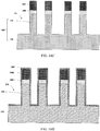
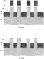
- FIGS. 2 through 15 are cross-sectional views illustrating intermediate stages of a varactor transistor manufactured with a method according to some embodiments of the present invention.
- the method may include the following process steps:
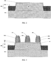
- FIG. 2 is a cross-sectional view illustrating an intermediate stage of a semiconductor structure according to S101.
- a semiconductor structure is provided.
- the semiconductor structure may include a semiconductor fin 220 having a first conductivity type and an initial insulator layer 230 on at least a portion of the surface of semiconductor fin 220.
- Semiconductor fin 220 may include silicon.
- Initial insulator layer 230 may include silicon dioxide. The manufacturing process of the semiconductor structure will be described in detail later below.
- the semiconductor structure may also include a substrate 210 having a second conductivity type that is different from the first conductivity type.
- the second conductivity type is n-type.
- the first conductivity type is n-type
- the second conductivity type is p-type.
- Semiconductor fin 220 is formed on substrate 210, and a reverse pn junction is formed between semiconductor fin 220 and substrate 210.
- the substrate may include silicon.
- the semiconductor structure may further include a trench isolation structure 240 surrounding semiconductor fin 220.
- Trench isolation structure 240 may include a trench 241 adjacent to semiconductor fin 220 and filled with a first insulator layer 242.
- First insulator layer 242 may include silicon dioxide.
- the method may further include forming a plurality of dummy gate structures surrounding a portion of the semiconductor fin.
- the dummy gate structures are separated from each other.
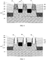
- FIG. 3 is a cross-sectional view illustrating an intermediate stage of a semiconductor device according to S102.
- a plurality of initial dummy gate structures are formed surrounding a portion of semiconductor fin 220.
- the plurality of initial dummy gate structures include at least an edge initial dummy gate structure on an edge of the semiconductor fin and a first initial dummy gate structure 351 spaced apart from edge initial dummy gate structure.
- Each of the plurality of initial dummy gate structures may include an initial dummy gate 3501 on a portion of the surface of initial insulator layer 230 and a spacer 3502 on sidewalls of initial dummy gate 3501.
- Initial dummy gate 3501 may include polysilicon.
- Spacer 3502 may include silicon nitride.
- the edge initial dummy gate structure may include a first edge dummy gate structure 352 on a first edge 221 of semiconductor fin 220 and a second edge dummy gate structure 353 on a second edge 222 of semiconductor fin 220.
- first edge 221 and second edge 222 are on opposite sides of first initial dummy gate structure 351. That is, first edge dummy gate structure 352 and second edge dummy gate structure 353 are disposed on opposite sides of first initial dummy gate structure 351.
- first initial dummy gate structure 351 is disposed between first edge dummy gate structure 352 and second edge dummy gate structure 353
- first edge dummy gate structure 352 and second edge dummy gate structure 353 may also be formed with a plurality of initial dummy gate structures separated from each other, so that the present invention is not limited to the case shown in FIG. 3 .
- first spacers spacers on opposite sides of first initial dummy gate structure 351 are referred to as first spacers
- spacers on opposite sides of first edge dummy gate structure 352 are referred to as second spacers
- spacers on opposite sides of second edge dummy gate structure 353 are referred to as third spacers.
- the closest distance between first and second spacers is referred to as a first distance.
- the distance between the first spacer on the left side of first initial dummy gate structure 351 and the second spacer on the right side of first edge dummy gate structure 352 is referred to as the first distance.
- the first distance may be 2 to 4 times the critical size of first initial dummy gate structure 351 (e.g., the cross-sectional width of first initial dummy gate structure 351 shown in FIG. 3 ), preferably 3 times.
- the closest distance between first and third spacers is referred to as a second distance.
- the distance between the first spacer on the right side of first initial dummy gate structure 351 and the third spacer on the left side of second edge dummy gate structure 353 is referred to as the second distance.
- the second distance may be 2 to 4 times the critical size of first initial dummy gate structure 351 (e.g., the cross-sectional width of first initial dummy gate structure 351 shown in FIG. 3 ), preferably 3 times.
- the method may further include forming a raised source/drain region on the semiconductor fin and between each of the initial dummy gate structures.
- FIG. 4 is a cross-sectional view illustrating an intermediate stage of a semiconductor device according to S103.
- a raised source/drain region is formed on semiconductor fin 220 and between each of the initial dummy gate structures through an etching process and an epitaxial process.
- the source/drain region may include a first source 461 disposed between first initial dummy gate structure 351 and first edge dummy gate structure 352.
- the source/drain region may include a first drain 462 disposed between first initial dummy gate structure 351 and second edge dummy gate structure 353.
- the method may also include performing an annealing process on the semiconductor structure after the source/drain region is formed.
- the method may further include forming an interlayer dielectric layer surrounding the plurality of initial dummy gate structures and the source/drain region and exposing an upper surface of the initial dummy gates of the plurality of initial dummy gate structures.
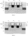
- FIG. 6 is a cross-sectional view illustrating an intermediate stage of a semiconductor device according to S104.
- an interlayer dielectric layer 570 is formed surrounding the plurality of initial dummy gate structures and the source/drain region and exposing an upper surface of the initial dummy gates 3501 of the plurality of initial dummy gate structures.
- Interlayer dielectric layer 570 may include silicon dioxide.
- S104 may include forming interlayer dielectric layer 570 on the substructure of FIG. 4 using a deposition process, as shown in FIG. 5 .
- S104 may also include planarizing (e.g., chemical mechanical polishing process) on interlayer dielectric layer 570 to expose an upper surface of the initial dummy gates of the plurality of initial dummy gate structures, e.g., exposing the upper surface of first initial dummy gate structure 351, first edge dummy gate structure 352, and second edge dummy gate structure 353.
- planarizing e.g., chemical mechanical polishing process
- the method may further include removing the exposed initial dummy gates and portions of the initial insulator layer below the exposed initial dummy gates to form a plurality of recesses.
- FIG. 7 is a cross-sectional view illustrating an intermediate stage of a semiconductor device according to S105. As shown in FIG. 7 , the exposed initial dummy gates 3501 and portions of the initial insulator layer below the exposed initial dummy gates are removed to form a plurality of recesses 780.
- the method may further include forming a gate insulator layer and a gate on the gate insulator layer in the plurality of recesses to form a plurality of gate structures that are separated from each other.
- the plurality of gate structures include at least a dummy gate structure on the edge of the semiconductor fin, and a first gate structure spaced apart from the dummy gate structure.
- FIG. 11 is a cross-sectional view illustrating an intermediate stage of a semiconductor device according to S106.
- a gate insulator layer 880 is formed in the plurality of recesses 780, and a gate 990 is formed on gate insulator layer 880 in the plurality of recesses to form a plurality of gate structures that are separated from each other.
- the plurality of gate structures include at least a dummy gate structure on the edge of the semiconductor fin, and a first gate structure 1102 is spaced apart from the dummy gate structure.
- the dummy gate structure may include a first dummy gate structure 1101 on first edge 221 of semiconductor fin 220 and a second dummy gate structure 1103 on second edge 222 of semiconductor fin 220.
- First dummy gate structure 1101 and second dummy gate structure 1103 are disposed on opposite sides of first gate structure 1102.
- first source 461 is disposed between first dummy gate structure 1101 and first gate structure 1102, i.e., the source/drain region may include first source 461.
- first drain 462 is disposed between second dummy gate structure 1103 and first dummy gate structure 1101, i.e., the source/drain region may include first gate drain 462.
- gate insulator layer 880 may include an interface layer (IL) 881 on a portion of the surface of the semiconductor fin and a high-k dielectric constant layer 882 on interface layer 881.
- the interface layer may include silicon dioxide.
- the high-k dielectric constant layer may include hafnium oxide (HfO 2 ), zirconium dioxide, or titanium dioxide.
- gate 990 may include a work function adjusting layer 991 on high-k dielectric constant layer 882, and a conductive material layer 992 on work function adjusting layer 991.
- work function adjusting layer 991 may be an NMOS work function adjusting layer.
- the NMOS work function adjusting layer may include titanium aluminum alloy (TiAl).
- work function adjusting layer 991 may be a PMOS work function adjusting layer.
- the PMOS work function adjusting layer may include titanium nitrite (TiN) or tantalum nitride (TaN).
- conductive material layer 992 may include a metal such as tungsten.
- step S106 The process of forming the gate insulator layer and the gate in the recesses (i.e., step S106) will be described in detail below with reference to FIGS. 8 through 11 .
- S106 may include forming an interface layer 881 on the bottom of recesses 780 using a deposition process and a high-k dielectric layer 882 on interface layer 881, as shown in FIG. 8 .
- interface layer 881 and high-k dielectric layer 882 together form a gate insulator layer 880.
- S106 may also include forming a work function adjusting layer 991 on an interlayer dielectric layer 570, sidewalls of recesses 780 and high-k dielectric layer 882 using a deposition process, as shown in FIG. 9 .
- S106 may further include forming a conductive material layer 992 on the structure shown in FIG. 9 using a deposition process to fill recesses 780, as shown in FIG. 10 .
- S106 may also include planarizing (e.g., using a chemical mechanical polishing process) on the structure shown in FIG. 10 to expose the upper surface of interlayer dielectric layer 570, thereby forming a plurality of gate structures separated from each other by interlayer dielectric layer 570, such as first dummy gate structure 1101, first gate structure 1102, and second dummy gate structure 1103, as shown in FIG. 11 .
- Work function adjusting layer 991 and conductive material layer 992 are collectively referred to as gate 990.
- the method may further include forming a first dielectric layer on the interlayer dielectric layer covering the plurality of gate structures.
- FIG. 12 is a cross-sectional view illustrating an intermediate stage of a semiconductor device according to S107.
- a first dielectric layer 1210 is formed on interlayer dielectric layer 570 covering the plurality of gate structures using, for example, a deposition process.
- the first dielectric layer may be an inter-metal dielectric (IMD) layer and include silicon dioxide.
- IMD inter-metal dielectric
- the method may further include forming a first contact through the first dielectric layer and the interlayer dielectric layer to the source or drain and a dummy gate contact through the first dielectric layer to the gates of the dummy gate structures.
- FIG. 14 is a cross-sectional view illustrating an intermediate stage of a semiconductor device according to S108.
- a first contact 1320 is formed through first dielectric layer 1210 and interlayer dielectric layer 570 to the source or drain and a dummy gate contact 1430 is formed through first dielectric layer 1210 to the gates of the dummy gate structures.
- first contact 1320 and dummy gate contact 1430 may include a metal such as copper or tungsten.
- first contact 1320 may include a first source contact 1321 to first source 461 and a first drain contact 1322 to first drain 462, as shown in FIG. 14 .
- dummy gate contact 1430 may include a first dummy gate contact 1431 to the gate of first dummy gate structure 1101 and a second dummy gate contact 1432 to the gate of second dummy gate structure 1103.
- step S108 The process of forming the first contact and the dummy gate contact (i.e., step S108) will be described in detail below with reference to FIGS. 13 and 14 .
- S108 may include forming a first contact 1320 through first dielectric layer 1210 and interlayer dielectric layer 570 to the source or drain, for example, forming a first source contact 1321 to a first source 461 and forming a a first drain contact 1322 to a first drain 462.
- a first though-hole may be first formed to the source/drain region, thereafter a metal such as copper or tungsten may be deposited to fill the first through-hole to form the first contact.
- S108 may also include forming a dummy gate contact 1430 through first dielectric layer 1210 to the gates of the dummy gate structures, for example, forming a first dummy gate contact 1431 to the gate of first dummy gate structure 1101 and forming a second dummy gate contact 1432 to the gate of first dummy gate structure 1103.
- a second through-hole may be first formed to the gates of the dummy gate structures, thereafter a metal such as copper or tungsten may be deposited to fill the second through-hole to form the dummy gate contact.
- first contact and the dummy gate contact The process of forming the first contact and the dummy gate contact is thus described in the above sections. Those skilled in the art will appreciate that the order of forming the first contact and the dummy gate contact is described as an example, and the present invention is not limited thereto.
- the dummy gate contact may be first formed, and the first contact is then formed.
- the present invention is not limited thereto.
- the method may further include forming a metal connector on the first dielectric layer in contact with the dummy gate contact and the first contact.
- FIG. 15 is a cross-sectional view illustrating an intermediate stage of a semiconductor device according to S109.
- a metal connector 1540 is formed on first dielectric layer 1210 in contact with dummy gate contact 1430 and in contact with first contact 1320.
- the metal connection may include copper, tungsten, or aluminum.
- metal connector 1540 is in contact with first dummy gate contact 1431, second dummy gate contact 1432, first source contact 1321, and first drain contact 1322. In one embodiment, metal connector 1540 is connected to ground.
- embodiments of the present invention provide a method of manufacturing a varactor transistor. Based on the described method, the source and drain of the transistor have a regular morphology.
- Embodiments of the present invention can reduce or eliminate the parasitic capacitance by electrically connecting the gates of the dummy gate structures to the source/drain region to the same potential to improve the stability of the device performance.
- embodiments of the present invention can increase the capacitor tuning range of a varactor transistor.
- the varactor tuning range is defined as the ratio of Cmax and Cmin, where Cmax is the maximum capacitance of the varactor and Cmin is the minimum capacitance of the varactor of the capacitance-voltage (C-V) characteristic curve.
- the minimum capacitance includes the parasitic capacitance. Since the parasitic capacitance has been reduced or eliminated according to the present invention, the minimum capacitance of the varactor is reduced so that the capacitance tuning range of the varactor is increased.
- the varactor transistor may include a semiconductor fin 220 having a fist conductivity type.
- the varactor transistor may further include a plurality of gate structures surrounding a portion of semiconductor fin 220 and separated from each other.
- the plurality of gate structures include at least a dummy gate structure on an edge of semiconductor fin 220 and a first gate structure 1102 spaced apart from the dummy gate structure.
- Each gate structure includes a gate insulator layer 880 on a portion of the surface of semiconductor fin 220, a gate 990 on gate insulator layer 880, a spacer 3502 on sidewalls of the gate.
- the dummy gate structure may include a first edge dummy gate structure 1101 on a first edge 221 of semiconductor fin 220 and a second edge dummy gate structure 1103 on a second edge 222 of semiconductor fin 220.
- First edge dummy gate structure 1101 and second edge dummy gate structure 1103 are disposed on opposite sides of first gate structure 1102.
- first edge 221 and second edge 222 are on opposite sides of first gate structure 1102.
- gate insulator layer 880 may include an interface layer 881 on a portion of the surface of semiconductor fin 220 and a high-k dielectric constant layer 882 on interface layer 881.
- the interface layer may include silicon dioxide.
- the high-k dielectric constant layer may include hafnium oxide (HfO 2 ), zirconium dioxide, or titanium dioxide.
- the gate includes a work function adjusting layer 991 on high-k dielectric constant layer 882, and a conductive material layer 992 on work function adjusting layer 991.
- work function adjusting layer 991 may be an NMOS work function adjusting layer.
- the NMOS work function adjusting layer may include titanium aluminum alloy (TiAl).
- work function adjusting layer 991 may be a PMOS work function adjusting layer.
- the PMOS work function adjusting layer may include titanium nitrite (TiN) or tantalum nitride (TaN).
- conductive material layer 992 may include a metal such as tungsten.
- the varactor transistor may further include a raised source/drain region on the semiconductor fin and disposed between the dummy gate structures and the first gate structure.
- the raised source/drain region has a regular morphology.
- the gate of a dummy gate structure is electrically connected to the raised source/drain region at the same potential.
- the dummy gate structure includes a gate connected to the source/drain region.
- the source/drain region may include a first source 461 disposed between first dummy gate structure 1101 and first gate structure 1102. In one embodiment, the source/drain region may include a drain 462 disposed between second dummy gate structure 1103 and first gate structure 1102. In an example embodiment, first source 461 of first dummy gate structure 1101 and first drain 462 of second dummy gate structure 1103 are electrically connected to the same potential.
- parasitic capacitance can be eliminated as much as possible by connecting the gates of the dummy gate structures to the same potential as the source or drain so that the device performance is more stable, and the varactor transistor has a larger tuning range.
- the varactor transistor may also include a substrate 210 having a second conductivity type.
- the first conductivity type is p-type
- the second conductivity type is n-type.
- the first conductivity type is n-type
- the second conductivity type is p-type.
- Semiconductor fin 220 is formed on substrate 210, and a reverse pn junction is formed between semiconductor fin 220 and substrate 210.
- the varactor transistor may further include a first contact 1320 connected to the source and a dummy gate contact 1430 connected to the gate of the dummy gate structure.
- first contact 1320 may include a first contact 1320 may include a first source contact 1321 connected to first source 461 and a first drain contact 1322 connected to first drain 462.
- dummy gate contact 1430 may include a first dummy gate contact 1431 connected to the gate of first dummy gate structure 1101, and a second dummy gate contact 1432 connected to the gate of second dummy gate structure 1103.
- First source contact 1321, first drain contact 1322, first dummy gate contact 1431 and second dummy gate contact 1432 are connected to each other.
- first source contact 1321, first drain contact 1322, first dummy gate contact 1431 and second dummy gate contact 1432 are connected to ground.
- the varactor transistor may also include a trench isolation structure 240 disposed around semiconductor fin 220.
- Trench isolation structure 240 may include a trench 241 adjacent to semiconductor fin 220 and a first insulator layer 242 filling trench 241.
- First insulator layer 242 may include silicon dioxide.
- the varactor transistor may also include an interlayer dielectric layer 570 on first insulator layer 242 and surrounding the plurality of gate structures and a portion of first source contact 1321 and a portion of first drain contact 1322.
- Interlayer dielectric layer 570 may include a silicon dioxide.
- the varactor transistor may also include a first dielectric layer 1210 on interlayer dielectric layer 570 and surrounding first dummy gate contact 1431, second dummy gate contact 1432, a portion of first source contact 1321 and a portion of first drain contact 1322.
- First dielectric layer 1210 exposes an upper surface of first dummy gate contact 1431, second dummy gate contact 1432, first source contact 1321, and first drain contact 1322.
- the upper surface of first dielectric layer 1210 is flush with the upper surface of first dummy gate contact 1431, second dummy gate contact 1432, first source contact 1321, and first drain contact 1322.
- the first dielectric layer may include silicon dioxide.
- the varactor transistor may also include a metal connector 1540 on first dielectric layer 1210 and electrically in contact with first dummy gate contact 1431, second dummy gate contact 1432, first source contact 1321, and first drain contact 1322.
- the metal connector may include copper, tungsten or aluminum.
- Metal connector 1540 electrically connects first dummy gate contact 1431, second dummy gate contact 1432, first source contact 1321, and first drain contact 1322 to the same potential. That is, the metal connector is such that the gates of the dummy gate structures are connected to the same potential as the source or drain, so that parasitic capacitance can be reduced or eliminated to obtain a stable performance and a larger capacitor tuning range of the varactor transistor.
- connection of the gates of the dummy gate structures to the source or drain in the above-described manner is exemplary only, the present invention is not limited thereto.
- Other manners and configurations of the connection of the gates of the dummy gate structures to the source or drain so that they have the same potential will fall within the scope of the invention which is defined by the claims.
- the varactor transistor may also include an initial insulator layer 230 disposed between interlayer dielectric layer 570 and semiconductor fin 220.
- the initial insulator layer may include silicon dioxide.
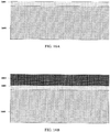
- FIGS. 16A-16J are cross-sectional views illustrating intermediate stage of a semiconductor structure manufactured with a method according to some embodiments of the present invention. A method of manufacturing a semiconductor structure according to some embodiments of the present invention will be described in detail with reference to FIGS. 16A through 16J .
- a second insulator layer 1601 is formed as a buffer layer on a semiconductor substrate (e.g., a silicon substrate) 1600 using a deposition process.
- Second insulator layer 1601 may include silicon dioxide.
- a doping (e.g., an ion implantation) process is performed into semiconductor substrate 1600 such that the semiconductor substrate is doped with a second conductivity type.
- Hardmask layer 1602 is formed on second insulator layer 1601 using, for example, a deposition process.
- Hardmask layer 1602 may include silicon nitride.
- an etching process (e.g., using photolithography and etching processes) is performed on the structure shown in FIG. 16B to form a plurality of semiconductor fins 220.
- the portion below the semiconductor fins is substrate 210.
- a third insulator layer 1603 is formed on the structure shown in FIG. 16D using, for example, a deposition process.
- Third insulator layer 1603 may include silicon dioxide.
- a first insulator layer 242 is formed on the structure shown in FIG. 16D using, for example, a deposition process such as a flowable chemical vapor deposition (FCVD) process to fill trenches 241 between the respective semiconductor fins.
- a deposition process such as a flowable chemical vapor deposition (FCVD) process to fill trenches 241 between the respective semiconductor fins.
- FCVD flowable chemical vapor deposition
- first insulator layer 242 and third insulator layer 1603 are planarization processes to expose an upper surface of hardmask layer 1602.
- first insulator layer 242 and third insulator layer 1603 are etched back so that the semiconductor fins protrude from first insulator layer 242.
- hardmask layer 1602 abd second insulator layer 1601 are removed.
- a doping (e.g., ion implantation) process is performed on semiconductor fins 220 such that the semiconductor fins have a first conductivity type that is different from the second conductivity type of substrate 210.
- an initial insulator layer 230 is formed on a portion of the surface of semiconductor fins 220 using, for example, an oxidation process.
- initial insulator layer 230 may be formed using a deposition process.
- embodiments of the present invention provide a method of manufacturing a semiconductor structure.
- the cross-sectional view of the semiconductor structure shown in FIG. 2 can be considered as a cross-sectional view of the structure taken along the line A-A' in FIG. 16J .
- Third layer 1603 in FIG. 16J is omitted in FIG. 2 .
- the semiconductor structure may further include a third insulator layer 1603 disposed between first insulator layer 242 and substrate 210 and between first insulator layer 242 and semiconductor fin 210. In other embodiments, the semiconductor structure may not include the third insulator layer.
- embodiments of the present invention provide detailed description of method of manufacturing a semiconductor device and a semiconductor structure, and a semiconductor device manufactured using the described methods.
- numerous specific details such as formation of fins, source, drain, trenches, and the like have not been described in detail in order not to obscure the embodiments of the invention.
- references in the specification to "one embodiment”, “an embodiment”, “an example embodiment”, “some embodiments”, etc., indicate that the embodiment described may include a particular feature, structure, or characteristic, but every embodiment may not necessarily include the particular feature, structure, or characteristic. Moreover, such phrases are not necessarily referring to the same embodiment. Further, when a particular feature, structure, or characteristic is described in connection with an embodiment, it is submitted that it is within the knowledge of one skilled in the art to affect such feature, structure, or characteristic in connection with other embodiments whether or not explicitly described.
Landscapes
- Insulated Gate Type Field-Effect Transistor (AREA)
- Engineering & Computer Science (AREA)
- Power Engineering (AREA)
- Thin Film Transistor (AREA)
- Electrodes Of Semiconductors (AREA)
- Chemical & Material Sciences (AREA)
- Composite Materials (AREA)
- Materials Engineering (AREA)
Abstract
Description
- The present application claims priority to Chinese patent application No.
201610512157.1 - The present invention relates to integrated semiconductor devices, and more particularly to a FinFET varactor and method for manufacturing the same.
- As the critical dimension of metal oxide semiconductor field effect transistor (MOSFET) devices continues to shrink, the short channel effect becomes more problematic. Fin field effect transistor (FinFET) devices have good control capability of gates to effectively suppress the short channel effect. FinFET devices can also reduce random dopant fluctuation to improve the device stability. Thus, FinFET devices are widely used in the design of small-sized semiconductor elements.
- In radio frequency (RF) circuits, the variable capacitance (varactor) MOS transistor is an important component. In the manufacturing process of a fin-type varactor MOS transistor, after the removal of an initial dummy gate polysilicon, the epitaxially formed source and drain have an irregular morphology, thereby affecting the device performance.
- It is an object of the present invention to provide an improved varactor MOS transistor and a manufacturing process for a fin-type varactor MOS transistor, in which an irregular morphology of the epitaxially formed source and drain can be avoided so that the device performance is not affected.
- The object is achieved by the features of the respective independent claims. Further embodiments are defined in the respective dependent claims.
- In particular, the present inventor discovered that the epitaxial morphology of the source and drain of a FinFET is affected by the removal of the dummy polysilicon gate and provides a novel varactor design and method of manufacturing the same to overcome the problems.
- A first aspect of the present invention provides a varactor transistor. The varactor transistor includes a semiconductor fin having a first conductivity type, a plurality of gate structures separated from each other and surrounding a portion of the semiconductor fin. The plurality of gates structures include a dummy gate structure on an edge of the semiconductor fin and a first gate structure spaced apart from the dummy gate structure. The dummy gate structure and the gate structure each include a gate insulator layer on a surface portion of the semiconductor fin, a gate on the gate insulator layer, and a spacer on the gate. The varactor transistor also includes a raised source/drain region on the semiconductor fin and between the dummy gate structure and the first gate structure. The raised source/drain region and the gate of the dummy gate structure are electrically connected to a same potential.
- Preferably, the varactor transistor further includes a substrate having a second conductivity type different from the first conductivity type, the semiconductor fin on the substrate and a reverse pn junction formed between the semiconductor fin and the substrate.
- Preferably, the dummy gate structure includes a first dummy gate structure on a first edge of the semiconductor fin and a second dummy gate structure on a second edge of the semiconductor fin, the first and second dummy gate structures are disposed on opposite sides of the fist gate structure.
- Preferably, the raised source/drain region includes a source disposed between the first dummy gate structure and the first gate structure, and a drain disposed between the second dummy gate structure and the first gate structure.
- Preferably, the varactor transistor further includes a first contact to the raised source/drain region and a dummy gate contact to the gate of the dummy gate structure, the first contact and the dummy gate contact are electrically connected to each other.
- Preferably, the first contact includes a source contact connected to the source and a drain contact connected to the drain. The dummy gate contact includes a first dummy gate contact connected to the gate of the first dummy gate structure and a second dummy gate contact connected to the gate of the second dummy gate structure. The source contact, the drain contact, the first dummy gate contact and second dummy gate contact are connected to each other. In one embodiment, the source contact, the drain contact, the first dummy gate contact and second dummy gate contact are connected to ground.
- Preferably, the varactor transistor further includes a trench isolation structure around the semiconductor fin and having a trench adjacent to the semiconductor fin and a first insulating layer in the trench.
- Preferably, the varactor transistor further includes an interlayer dielectric layer surrounding the plurality of gate structures and a portion of the source contact and a portion of the drain contact on the first insulator layer.
- Preferably, the varactor transistor further includes a first dielectric layer surrounding the first dummy gate contact, a portion of the first source contact and a portion of the first drain contact. The first dielectric layer exposes an upper surface of the first dummy gate contact, the second dummy gate contact, the source contact, and the drain contact.
- Preferably, the varactor transistor further includes a metal connector on the first dielectric layer and in contact with the first dummy gate contact, the second dummy gate contact, the source contact, and the drain contact.
- Preferably, the varactor transistor further includes an initial insulator layer between the interlayer dielectric layer and the semiconductor fin.
- Preferably, the gate insulator layer includes an interface layer on a surface portion of the semiconductor fin and a high-k dielectric layer on the interface layer. The gate includes a work function adjusting layer on the high-k dielectric layer on the interface layer and a conductive material layer on the work function adjusting layer.
- A second aspect of the present invention provides a method of manufacturing a varactor transistor. The method includes providing a semiconductor structure including a semiconductor fin having a first conductivity type and an initial insulator layer on the semiconductor fin, and forming a plurality of initial dummy gate structures separated from each other and surrounding a portion of the semiconductor fin. The plurality of initial dummy gate structures includes at least an edge initial dummy gate structure on an edge of the semiconductor fin, and a first initial dummy gate structure spaced apart from the edge initial dummy gate structure, the edge initial dummy gate structure and the first initial dummy gate structure each including an initial gate insulator layer on a surface portion of the semiconductor fin, an initial gate on the initial gate insulator layer, and a spacer on the initial gate. The method also includes forming a raised source/drain region on the semiconductor fin and between each of the initial dummy gate structures, forming an interlayer dielectric layer surrounding the plurality of initial dummy gate structures and the raised source/drain region and exposing an upper surface of the initial gates of the plurality of initial dummy gate structures, removing the exposed initial gates and portions of the initial insulator layers below the exposed initial gates to form a plurality of recesses, and forming a gate insulator layer in the plurality of recesses and gates on the gate insulator to form a plurality of gates structures separated from each other. The plurality of gates structures include at least a dummy gate structure on the edge of the semiconductor fin and a first gate structure spaced apart from the dummy gate structure. The method further includes forming a first dielectric layer on the interlayer dielectric layer covering the plurality of gates structures, forming a first contact through the first dielectric layer and the interlayer dielectric layer to the source/drain region and a dummy gate contact through the first dielectric layer to the gate of the dummy gate structure, and forming a metal connector on the first dielectric layer in contact with the dummy gate contact and the first contact.
- Preferably, the dummy gate structure includes a first edge dummy gate structure on a first edge of the semiconductor fin and a second edge dummy gate structure on a second edge of the semiconductor fin, the first and second edge dummy gate structures being disposed on opposite sides of the first gate structure.
- Preferably, the raised source/drain region includes a source disposed between the first dummy gate structure and the first gate structure, and a drain disposed between the second dummy gate structure and the first gate structure.
- Preferably, the first contact includes a source contact connected to the source and a drain contact connected to the drain. The dummy gate contact includes a first dummy gate contact connected to a gate of the first edge dummy gate structure and a second dummy gate contact connected to a gate of the second edge dummy gate structure. The metal connector connects to the source contact, the drain contact, the first dummy gate contact and the second dummy gate contact.
- Preferably, the semiconductor structure further includes a trench isolation structure around the semiconductor fin, the trench isolation structure includes a trench adjacent to the semiconductor fin and a first insulator layer in the trench.
- Preferably, the gate insulator layer includes an interface layer on a portion of a surface of the semiconductor fin and a high-k dielectric layer on the interface layer. In one embodiment, the gate includes a work function adjusting layer on the high-k dielectric layer, and a conductive material layer on the work function adjusting layer.
- A varactor transistor according to the first aspect of the present invention may be obtained by a method according to the second aspect of the present invention.
- The following detailed description together with the accompanying drawings will provide a better understanding of the nature and advantages of the present invention.
-
-
FIG. 1 is a flowchart of a method for manufacturing a varactor transistor according to some embodiments of the present invention. -
FIGS. 2-15 are cross-sectional views illustrating intermediate stages of a varactor transistor manufactured with a method according to some embodiments of the present invention. -
FIGS. 16A-16J are cross-sectional views illustrating intermediate stage of a semiconductor structure manufactured with a method according to some embodiments of the present invention. - Embodiments of the present invention now will be described more fully hereinafter with reference to the accompanying drawings. The invention may, however, be embodied in many different forms and should not be construed as limited to the embodiments set forth herein. Rather, these embodiments are provided so that this disclosure will be thorough and complete, and will fully convey the present invention to those skilled in the art. The features may not be drawn to scale, some details may be exaggerated relative to other elements for clarity. Like numbers refer to like elements throughout.
- It will be understood that when an element such as a layer, region or substrate is referred to as being "on" or extending "onto" another element, it can be directly on or extend directly onto the other element or intervening elements may also be present. In contrast, when an element is referred to as being "directly on" or extending "directly onto" another element, there are no intervening elements present. It will also be understood that when an element is referred to as being "connected" or "coupled" to another element, it can be directly connected or coupled to the other element or intervening elements may be present. In contrast, when an element is referred to as being "directly connected" or "directly coupled" to another element, there are no intervening elements present.
- Relative terms such as "below" or "above" or "upper" or "lower" or "horizontal" or "lateral" or "vertical" may be used herein to describe a relationship of one element, layer or region to another element, layer or region as illustrated in the figures. It will be understood that these terms are intended to encompass different orientations of the device in addition to the orientation depicted in the figures.
- The terminology used herein is for the purpose of describing particular embodiments only and is not intended to be limiting of the invention. As used herein, the singular forms "a", "an", and "the" are intended to include the plural forms as well, unless the context clearly indicates otherwise. It will be further understood that the terms "comprises", "comprising", "includes", and/or "including" when used herein, specify the presence of stated features, integers, steps, operations, elements, and/or components, but do not preclude the presence or addition of one or more other features, integers, steps, operations, elements, components, and/or groups thereof.
- Embodiments of the invention are described herein with reference to cross-sectional illustrations that are schematic illustrations of idealized embodiments (and intermediate structures) of the invention. The thickness of layers and regions in the drawings may be enlarged relative to other layers and regions for clarity. Additionally, variations from the shapes of the illustrations as a result, for example, of manufacturing techniques and/or tolerances, are to be expected. Thus, embodiments of the invention should not be construed as limited to the particular shapes of regions illustrated herein but are to include deviations in shapes that result, for example, from manufacturing. For example, an implanted region illustrated as a rectangle will, typically, have rounded or curved features and/or a gradient of implant concentration at its edges rather than a discrete change from implanted to non-implanted region. Likewise, a buried region formed by implantation may result in some implantation in the region between the buried region and the surface through which the implantation takes place. Thus, the regions illustrated in the figures are schematic in nature and their shapes are not intended to illustrate the actual shape of a region of a device and are not intended to limit the invention.
- Embodiments of the present invention now will be described more fully hereinafter with reference to the accompanying drawings, in which embodiments of the invention are shown. This invention may, however, be embodied in many different forms and should not be construed as limited to the embodiments set forth herein.
-
FIG. 1 is a flowchart of a method for manufacturing a varactor transistor according to some embodiments of the present invention.FIGS. 2 through 15 are cross-sectional views illustrating intermediate stages of a varactor transistor manufactured with a method according to some embodiments of the present invention. - Referring to
FIG. 1 , the method may include the following process steps: - At S101: providing a semiconductor structure. The semiconductor structure includes a semiconductor fin having a having a first conductivity type and an initial insulator layer on at least a portion of the surface of the semiconductor fin.
-
FIG. 2 is a cross-sectional view illustrating an intermediate stage of a semiconductor structure according to S101. As shown inFIG. 2 , a semiconductor structure is provided. The semiconductor structure may include asemiconductor fin 220 having a first conductivity type and aninitial insulator layer 230 on at least a portion of the surface ofsemiconductor fin 220.Semiconductor fin 220 may include silicon.Initial insulator layer 230 may include silicon dioxide. The manufacturing process of the semiconductor structure will be described in detail later below. - In one embodiment, as shown in
FIG. 2 , the semiconductor structure may also include asubstrate 210 having a second conductivity type that is different from the first conductivity type. For example, when the first conductivity type is p-type, the second conductivity type is n-type. Conversely, when the first conductivity type is n-type, the second conductivity type is p-type.Semiconductor fin 220 is formed onsubstrate 210, and a reverse pn junction is formed betweensemiconductor fin 220 andsubstrate 210. The substrate may include silicon. - In one embodiment, still referring to
FIG. 2 , the semiconductor structure may further include atrench isolation structure 240 surroundingsemiconductor fin 220. Trenchisolation structure 240 may include atrench 241 adjacent tosemiconductor fin 220 and filled with afirst insulator layer 242.First insulator layer 242 may include silicon dioxide. - Referring back to
FIG. 1 , at S102, the method may further include forming a plurality of dummy gate structures surrounding a portion of the semiconductor fin. The dummy gate structures are separated from each other. -
FIG. 3 is a cross-sectional view illustrating an intermediate stage of a semiconductor device according to S102. As shown inFIG. 3 , a plurality of initial dummy gate structures are formed surrounding a portion ofsemiconductor fin 220. The plurality of initial dummy gate structures include at least an edge initial dummy gate structure on an edge of the semiconductor fin and a first initialdummy gate structure 351 spaced apart from edge initial dummy gate structure. Each of the plurality of initial dummy gate structures may include aninitial dummy gate 3501 on a portion of the surface ofinitial insulator layer 230 and aspacer 3502 on sidewalls ofinitial dummy gate 3501.Initial dummy gate 3501 may include polysilicon.Spacer 3502 may include silicon nitride. - In one embodiment, at S102, as shown in
FIG. 3 , the edge initial dummy gate structure may include a first edgedummy gate structure 352 on afirst edge 221 ofsemiconductor fin 220 and a second edgedummy gate structure 353 on asecond edge 222 ofsemiconductor fin 220. Herein,first edge 221 andsecond edge 222 are on opposite sides of first initialdummy gate structure 351. That is, first edgedummy gate structure 352 and second edgedummy gate structure 353 are disposed on opposite sides of first initialdummy gate structure 351. - It should be noted that, although
FIG. 3 shows that first initialdummy gate structure 351 is disposed between first edgedummy gate structure 352 and second edgedummy gate structure 353, those skilled in the art will appreciate that first edgedummy gate structure 352 and second edgedummy gate structure 353 may also be formed with a plurality of initial dummy gate structures separated from each other, so that the present invention is not limited to the case shown inFIG. 3 . - In one embodiment, spacers on opposite sides of first initial
dummy gate structure 351 are referred to as first spacers, spacers on opposite sides of first edgedummy gate structure 352 are referred to as second spacers, and spacers on opposite sides of second edgedummy gate structure 353 are referred to as third spacers. - In one embodiment, the closest distance between first and second spacers is referred to as a first distance. Referring to
FIG. 3 , the distance between the first spacer on the left side of first initialdummy gate structure 351 and the second spacer on the right side of first edgedummy gate structure 352 is referred to as the first distance. In one embodiment, the first distance may be 2 to 4 times the critical size of first initial dummy gate structure 351 (e.g., the cross-sectional width of first initialdummy gate structure 351 shown inFIG. 3 ), preferably 3 times. - In one embodiment, the closest distance between first and third spacers is referred to as a second distance. Referring to
FIG. 3 , the distance between the first spacer on the right side of first initialdummy gate structure 351 and the third spacer on the left side of second edgedummy gate structure 353 is referred to as the second distance. In one embodiment, the second distance may be 2 to 4 times the critical size of first initial dummy gate structure 351 (e.g., the cross-sectional width of first initialdummy gate structure 351 shown inFIG. 3 ), preferably 3 times. - Referring back to
FIG. 1 , at S103, the method may further include forming a raised source/drain region on the semiconductor fin and between each of the initial dummy gate structures. -
FIG. 4 is a cross-sectional view illustrating an intermediate stage of a semiconductor device according to S103. As shown inFIG. 4 , a raised source/drain region is formed onsemiconductor fin 220 and between each of the initial dummy gate structures through an etching process and an epitaxial process. In one embodiment, the source/drain region may include afirst source 461 disposed between first initialdummy gate structure 351 and first edgedummy gate structure 352. In one embodiment, the source/drain region may include afirst drain 462 disposed between first initialdummy gate structure 351 and second edgedummy gate structure 353. - In one embodiment, the method may also include performing an annealing process on the semiconductor structure after the source/drain region is formed.
- Referring back to
FIG. 1 , at S104, the method may further include forming an interlayer dielectric layer surrounding the plurality of initial dummy gate structures and the source/drain region and exposing an upper surface of the initial dummy gates of the plurality of initial dummy gate structures. -
FIG. 6 is a cross-sectional view illustrating an intermediate stage of a semiconductor device according to S104. As shown inFIG. 6 , aninterlayer dielectric layer 570 is formed surrounding the plurality of initial dummy gate structures and the source/drain region and exposing an upper surface of theinitial dummy gates 3501 of the plurality of initial dummy gate structures.Interlayer dielectric layer 570 may include silicon dioxide. - Processes of S104 will be described with reference to
FIGS. 5 and6 . In one embodiment, S104 may include forminginterlayer dielectric layer 570 on the substructure ofFIG. 4 using a deposition process, as shown inFIG. 5 . Optionally, S104 may also include planarizing (e.g., chemical mechanical polishing process) oninterlayer dielectric layer 570 to expose an upper surface of the initial dummy gates of the plurality of initial dummy gate structures, e.g., exposing the upper surface of first initialdummy gate structure 351, first edgedummy gate structure 352, and second edgedummy gate structure 353. - Referring back to
FIG. 1 , at S105, the method may further include removing the exposed initial dummy gates and portions of the initial insulator layer below the exposed initial dummy gates to form a plurality of recesses. -
FIG. 7 is a cross-sectional view illustrating an intermediate stage of a semiconductor device according to S105. As shown inFIG. 7 , the exposedinitial dummy gates 3501 and portions of the initial insulator layer below the exposed initial dummy gates are removed to form a plurality ofrecesses 780. - Referring back to
FIG. 1 , at S106, the method may further include forming a gate insulator layer and a gate on the gate insulator layer in the plurality of recesses to form a plurality of gate structures that are separated from each other. The plurality of gate structures include at least a dummy gate structure on the edge of the semiconductor fin, and a first gate structure spaced apart from the dummy gate structure. -
FIG. 11 is a cross-sectional view illustrating an intermediate stage of a semiconductor device according to S106. As shown inFIG. 11 , agate insulator layer 880 is formed in the plurality ofrecesses 780, and agate 990 is formed ongate insulator layer 880 in the plurality of recesses to form a plurality of gate structures that are separated from each other. The plurality of gate structures include at least a dummy gate structure on the edge of the semiconductor fin, and afirst gate structure 1102 is spaced apart from the dummy gate structure. - In one embodiment, the dummy gate structure may include a first
dummy gate structure 1101 onfirst edge 221 ofsemiconductor fin 220 and a seconddummy gate structure 1103 onsecond edge 222 ofsemiconductor fin 220. Firstdummy gate structure 1101 and seconddummy gate structure 1103 are disposed on opposite sides offirst gate structure 1102. - In one embodiment,
first source 461 is disposed between firstdummy gate structure 1101 andfirst gate structure 1102, i.e., the source/drain region may includefirst source 461. In one embodiment,first drain 462 is disposed between seconddummy gate structure 1103 and firstdummy gate structure 1101, i.e., the source/drain region may includefirst gate drain 462. - In one embodiment,
gate insulator layer 880 may include an interface layer (IL) 881 on a portion of the surface of the semiconductor fin and a high-k dielectricconstant layer 882 oninterface layer 881. The interface layer may include silicon dioxide. The high-k dielectric constant layer may include hafnium oxide (HfO2), zirconium dioxide, or titanium dioxide. - In one embodiment,
gate 990 may include a workfunction adjusting layer 991 on high-k dielectricconstant layer 882, and aconductive material layer 992 on workfunction adjusting layer 991. In the case wheresemiconductor fin 220 is p-type doped, workfunction adjusting layer 991 may be an NMOS work function adjusting layer. For example, the NMOS work function adjusting layer may include titanium aluminum alloy (TiAl). In the case wheresemiconductor fin 220 is n-type doped, workfunction adjusting layer 991 may be a PMOS work function adjusting layer. For example, the PMOS work function adjusting layer may include titanium nitrite (TiN) or tantalum nitride (TaN). In one embodiment,conductive material layer 992 may include a metal such as tungsten. - The process of forming the gate insulator layer and the gate in the recesses (i.e., step S106) will be described in detail below with reference to
FIGS. 8 through 11 . - In one embodiment, S106 may include forming an
interface layer 881 on the bottom ofrecesses 780 using a deposition process and a high-k dielectric layer 882 oninterface layer 881, as shown inFIG. 8 . In an example embodiment,interface layer 881 and high-k dielectric layer 882 together form agate insulator layer 880. - In one embodiment, S106 may also include forming a work
function adjusting layer 991 on aninterlayer dielectric layer 570, sidewalls ofrecesses 780 and high-k dielectric layer 882 using a deposition process, as shown inFIG. 9 . - In one embodiment, S106 may further include forming a
conductive material layer 992 on the structure shown inFIG. 9 using a deposition process to fillrecesses 780, as shown inFIG. 10 . - In one embodiment, S106 may also include planarizing (e.g., using a chemical mechanical polishing process) on the structure shown in
FIG. 10 to expose the upper surface ofinterlayer dielectric layer 570, thereby forming a plurality of gate structures separated from each other byinterlayer dielectric layer 570, such as firstdummy gate structure 1101,first gate structure 1102, and seconddummy gate structure 1103, as shown inFIG. 11 . Workfunction adjusting layer 991 andconductive material layer 992 are collectively referred to asgate 990. - Referring back to
FIG. 1 , at S107, the method may further include forming a first dielectric layer on the interlayer dielectric layer covering the plurality of gate structures. -
FIG. 12 is a cross-sectional view illustrating an intermediate stage of a semiconductor device according to S107. As shown inFIG. 12 , afirst dielectric layer 1210 is formed oninterlayer dielectric layer 570 covering the plurality of gate structures using, for example, a deposition process. The first dielectric layer may be an inter-metal dielectric (IMD) layer and include silicon dioxide. - Referring back to
FIG. 1 , at S108, the method may further include forming a first contact through the first dielectric layer and the interlayer dielectric layer to the source or drain and a dummy gate contact through the first dielectric layer to the gates of the dummy gate structures. -
FIG. 14 is a cross-sectional view illustrating an intermediate stage of a semiconductor device according to S108. As shown inFIG. 14 , afirst contact 1320 is formed throughfirst dielectric layer 1210 andinterlayer dielectric layer 570 to the source or drain and adummy gate contact 1430 is formed throughfirst dielectric layer 1210 to the gates of the dummy gate structures. In an example embodiment,first contact 1320 anddummy gate contact 1430 may include a metal such as copper or tungsten. - In one embodiment,
first contact 1320 may include afirst source contact 1321 tofirst source 461 and afirst drain contact 1322 tofirst drain 462, as shown inFIG. 14 . - In one embodiment,
dummy gate contact 1430 may include a firstdummy gate contact 1431 to the gate of firstdummy gate structure 1101 and a seconddummy gate contact 1432 to the gate of seconddummy gate structure 1103. - The process of forming the first contact and the dummy gate contact (i.e., step S108) will be described in detail below with reference to
FIGS. 13 and14 . - In one embodiment, referring to
FIG. 13 , S108 may include forming afirst contact 1320 throughfirst dielectric layer 1210 andinterlayer dielectric layer 570 to the source or drain, for example, forming afirst source contact 1321 to afirst source 461 and forming a afirst drain contact 1322 to afirst drain 462. In one embodiment, a first though-hole may be first formed to the source/drain region, thereafter a metal such as copper or tungsten may be deposited to fill the first through-hole to form the first contact. - In one embodiment, referring to
FIG. 14 , S108 may also include forming adummy gate contact 1430 throughfirst dielectric layer 1210 to the gates of the dummy gate structures, for example, forming a firstdummy gate contact 1431 to the gate of firstdummy gate structure 1101 and forming a seconddummy gate contact 1432 to the gate of firstdummy gate structure 1103. In one embodiment, a second through-hole may be first formed to the gates of the dummy gate structures, thereafter a metal such as copper or tungsten may be deposited to fill the second through-hole to form the dummy gate contact. - The process of forming the first contact and the dummy gate contact is thus described in the above sections. Those skilled in the art will appreciate that the order of forming the first contact and the dummy gate contact is described as an example, and the present invention is not limited thereto. For example, the dummy gate contact may be first formed, and the first contact is then formed. Thus, the present invention is not limited thereto.
- Referring back to
FIG. 1 , at S109, the method may further include forming a metal connector on the first dielectric layer in contact with the dummy gate contact and the first contact. -
FIG. 15 is a cross-sectional view illustrating an intermediate stage of a semiconductor device according to S109. As shown inFIG. 15 , ametal connector 1540 is formed onfirst dielectric layer 1210 in contact withdummy gate contact 1430 and in contact withfirst contact 1320. In one embodiment, the metal connection may include copper, tungsten, or aluminum. By forming the metal connector, the gates of the dummy gate structures are electrically connected to the source or drain to the same potential. - In one embodiment,
metal connector 1540 is in contact with firstdummy gate contact 1431, seconddummy gate contact 1432,first source contact 1321, andfirst drain contact 1322. In one embodiment,metal connector 1540 is connected to ground. - Thus, embodiments of the present invention provide a method of manufacturing a varactor transistor. Based on the described method, the source and drain of the transistor have a regular morphology.
- The present inventor discovered that, if the dummy gate structures are at a floating state, there may be a potential difference between dummy gate structures and the first contact due to capacitive coupling, thereby generating parasitic capacitance that may affect the device performance. In the case where the distance between the first contact and the spacers of the dummy gate structures is reduced, the parasitic capacitance will increase, which worsens the problem. Embodiments of the present invention can reduce or eliminate the parasitic capacitance by electrically connecting the gates of the dummy gate structures to the source/drain region to the same potential to improve the stability of the device performance.
- Further, embodiments of the present invention can increase the capacitor tuning range of a varactor transistor. The varactor tuning range is defined as the ratio of Cmax and Cmin, where Cmax is the maximum capacitance of the varactor and Cmin is the minimum capacitance of the varactor of the capacitance-voltage (C-V) characteristic curve. The minimum capacitance includes the parasitic capacitance. Since the parasitic capacitance has been reduced or eliminated according to the present invention, the minimum capacitance of the varactor is reduced so that the capacitance tuning range of the varactor is increased.
- Embodiments of the present invention also provide a varactor transistor. Referring to
FIG. 15 , the varactor transistor may include asemiconductor fin 220 having a fist conductivity type. The varactor transistor may further include a plurality of gate structures surrounding a portion ofsemiconductor fin 220 and separated from each other. The plurality of gate structures include at least a dummy gate structure on an edge ofsemiconductor fin 220 and afirst gate structure 1102 spaced apart from the dummy gate structure. Each gate structure includes agate insulator layer 880 on a portion of the surface ofsemiconductor fin 220, agate 990 ongate insulator layer 880, aspacer 3502 on sidewalls of the gate. - In one embodiment, the dummy gate structure may include a first edge
dummy gate structure 1101 on afirst edge 221 ofsemiconductor fin 220 and a second edgedummy gate structure 1103 on asecond edge 222 ofsemiconductor fin 220. First edgedummy gate structure 1101 and second edgedummy gate structure 1103 are disposed on opposite sides offirst gate structure 1102. Herein,first edge 221 andsecond edge 222 are on opposite sides offirst gate structure 1102. - In one embodiment,
gate insulator layer 880 may include aninterface layer 881 on a portion of the surface ofsemiconductor fin 220 and a high-k dielectricconstant layer 882 oninterface layer 881. The interface layer may include silicon dioxide. The high-k dielectric constant layer may include hafnium oxide (HfO2), zirconium dioxide, or titanium dioxide. - In one embodiment, the gate includes a work
function adjusting layer 991 on high-k dielectricconstant layer 882, and aconductive material layer 992 on workfunction adjusting layer 991. In the case wheresemiconductor fin 220 is p-type doped, workfunction adjusting layer 991 may be an NMOS work function adjusting layer. For example, the NMOS work function adjusting layer may include titanium aluminum alloy (TiAl). In the case wheresemiconductor fin 220 is n-type doped, workfunction adjusting layer 991 may be a PMOS work function adjusting layer. For example, the PMOS work function adjusting layer may include titanium nitrite (TiN) or tantalum nitride (TaN). In one embodiment,conductive material layer 992 may include a metal such as tungsten. - In one embodiment, the varactor transistor may further include a raised source/drain region on the semiconductor fin and disposed between the dummy gate structures and the first gate structure. The raised source/drain region has a regular morphology. The gate of a dummy gate structure is electrically connected to the raised source/drain region at the same potential. For example, the dummy gate structure includes a gate connected to the source/drain region.
- In one embodiment, the source/drain region may include a
first source 461 disposed between firstdummy gate structure 1101 andfirst gate structure 1102. In one embodiment, the source/drain region may include adrain 462 disposed between seconddummy gate structure 1103 andfirst gate structure 1102. In an example embodiment,first source 461 of firstdummy gate structure 1101 andfirst drain 462 of seconddummy gate structure 1103 are electrically connected to the same potential. - According to embodiments of the present invention, parasitic capacitance can be eliminated as much as possible by connecting the gates of the dummy gate structures to the same potential as the source or drain so that the device performance is more stable, and the varactor transistor has a larger tuning range.
- In one embodiment, referring to
FIG. 15 , the varactor transistor may also include asubstrate 210 having a second conductivity type. In an example embodiment, the first conductivity type is p-type, and the second conductivity type is n-type. In another example embodiment, the first conductivity type is n-type, and the second conductivity type is p-type.Semiconductor fin 220 is formed onsubstrate 210, and a reverse pn junction is formed betweensemiconductor fin 220 andsubstrate 210. - In one embodiment, referring to
FIG. 15 , , the varactor transistor may further include afirst contact 1320 connected to the source and adummy gate contact 1430 connected to the gate of the dummy gate structure. - In one embodiment,
first contact 1320 may include afirst contact 1320 may include afirst source contact 1321 connected tofirst source 461 and afirst drain contact 1322 connected tofirst drain 462. In one embodiment,dummy gate contact 1430 may include a firstdummy gate contact 1431 connected to the gate of firstdummy gate structure 1101, and a seconddummy gate contact 1432 connected to the gate of seconddummy gate structure 1103.First source contact 1321,first drain contact 1322, firstdummy gate contact 1431 and seconddummy gate contact 1432 are connected to each other.. In one embodiment,first source contact 1321,first drain contact 1322, firstdummy gate contact 1431 and seconddummy gate contact 1432 are connected to ground. - In one embodiment, referring to
FIG. 15 , the varactor transistor may also include atrench isolation structure 240 disposed aroundsemiconductor fin 220. Trenchisolation structure 240 may include atrench 241 adjacent tosemiconductor fin 220 and afirst insulator layer 242filling trench 241.First insulator layer 242 may include silicon dioxide. - In one embodiment, referring to
FIG. 15 , the varactor transistor may also include aninterlayer dielectric layer 570 onfirst insulator layer 242 and surrounding the plurality of gate structures and a portion offirst source contact 1321 and a portion offirst drain contact 1322.Interlayer dielectric layer 570 may include a silicon dioxide. - In one embodiment, referring to
FIG. 15 , the varactor transistor may also include afirst dielectric layer 1210 oninterlayer dielectric layer 570 and surrounding firstdummy gate contact 1431, seconddummy gate contact 1432, a portion offirst source contact 1321 and a portion offirst drain contact 1322.First dielectric layer 1210 exposes an upper surface of firstdummy gate contact 1431, seconddummy gate contact 1432,first source contact 1321, andfirst drain contact 1322. In a preferred embodiment, the upper surface offirst dielectric layer 1210 is flush with the upper surface of firstdummy gate contact 1431, seconddummy gate contact 1432,first source contact 1321, andfirst drain contact 1322. The first dielectric layer may include silicon dioxide. - In one embodiment, referring to
FIG. 15 , the varactor transistor may also include ametal connector 1540 onfirst dielectric layer 1210 and electrically in contact with firstdummy gate contact 1431, seconddummy gate contact 1432,first source contact 1321, andfirst drain contact 1322. The metal connector may include copper, tungsten or aluminum.Metal connector 1540 electrically connects firstdummy gate contact 1431, seconddummy gate contact 1432,first source contact 1321, andfirst drain contact 1322 to the same potential. That is, the metal connector is such that the gates of the dummy gate structures are connected to the same potential as the source or drain, so that parasitic capacitance can be reduced or eliminated to obtain a stable performance and a larger capacitor tuning range of the varactor transistor. - Those of skill in the art will appreciate that the connection of the gates of the dummy gate structures to the source or drain in the above-described manner is exemplary only, the present invention is not limited thereto. Other manners and configurations of the connection of the gates of the dummy gate structures to the source or drain so that they have the same potential will fall within the scope of the invention which is defined by the claims.
- In one embodiment, referring to
FIG. 15 , the varactor transistor may also include aninitial insulator layer 230 disposed between interlayerdielectric layer 570 andsemiconductor fin 220. The initial insulator layer may include silicon dioxide. -
FIGS. 16A-16J are cross-sectional views illustrating intermediate stage of a semiconductor structure manufactured with a method according to some embodiments of the present invention. A method of manufacturing a semiconductor structure according to some embodiments of the present invention will be described in detail with reference toFIGS. 16A through 16J . - Referring to
FIG. 16A , asecond insulator layer 1601 is formed as a buffer layer on a semiconductor substrate (e.g., a silicon substrate) 1600 using a deposition process.Second insulator layer 1601 may include silicon dioxide. In one embodiment, a doping (e.g., an ion implantation) process is performed intosemiconductor substrate 1600 such that the semiconductor substrate is doped with a second conductivity type. - Next, referring to
FIG. 16B , ahardmask layer 1602 is formed onsecond insulator layer 1601 using, for example, a deposition process.Hardmask layer 1602 may include silicon nitride. - Next, referring to
FIG. 16C , an etching process (e.g., using photolithography and etching processes) is performed on the structure shown inFIG. 16B to form a plurality ofsemiconductor fins 220. The portion below the semiconductor fins issubstrate 210. - Next, referring to
FIG. 16D , athird insulator layer 1603 is formed on the structure shown inFIG. 16D using, for example, a deposition process.Third insulator layer 1603 may include silicon dioxide. - Next, referring to
FIG. 16E , afirst insulator layer 242 is formed on the structure shown inFIG. 16D using, for example, a deposition process such as a flowable chemical vapor deposition (FCVD) process to filltrenches 241 between the respective semiconductor fins. - Next, referring to
FIG. 16F , a planarization process is performed onfirst insulator layer 242 andthird insulator layer 1603 to expose an upper surface ofhardmask layer 1602. - Next, referring to
FIG. 16G ,first insulator layer 242 andthird insulator layer 1603 are etched back so that the semiconductor fins protrude fromfirst insulator layer 242. - Next, referring to
FIG. 16H ,hardmask layer 1602 abdsecond insulator layer 1601 are removed. - Next, referring to
FIG. 16I , a doping (e.g., ion implantation) process is performed onsemiconductor fins 220 such that the semiconductor fins have a first conductivity type that is different from the second conductivity type ofsubstrate 210. - Next, referring to
FIG. 16J , aninitial insulator layer 230 is formed on a portion of the surface ofsemiconductor fins 220 using, for example, an oxidation process. In another embodiment,initial insulator layer 230 may be formed using a deposition process. - Thus, embodiments of the present invention provide a method of manufacturing a semiconductor structure. The cross-sectional view of the semiconductor structure shown in
FIG. 2 can be considered as a cross-sectional view of the structure taken along the line A-A' inFIG. 16J .Third layer 1603 inFIG. 16J is omitted inFIG. 2 . In some embodiments, the semiconductor structure may further include athird insulator layer 1603 disposed betweenfirst insulator layer 242 andsubstrate 210 and betweenfirst insulator layer 242 andsemiconductor fin 210. In other embodiments, the semiconductor structure may not include the third insulator layer. - Thus, embodiments of the present invention provide detailed description of method of manufacturing a semiconductor device and a semiconductor structure, and a semiconductor device manufactured using the described methods. In the description, numerous specific details such as formation of fins, source, drain, trenches, and the like have not been described in detail in order not to obscure the embodiments of the invention.
- References in the specification to "one embodiment", "an embodiment", "an example embodiment", "some embodiments", etc., indicate that the embodiment described may include a particular feature, structure, or characteristic, but every embodiment may not necessarily include the particular feature, structure, or characteristic. Moreover, such phrases are not necessarily referring to the same embodiment. Further, when a particular feature, structure, or characteristic is described in connection with an embodiment, it is submitted that it is within the knowledge of one skilled in the art to affect such feature, structure, or characteristic in connection with other embodiments whether or not explicitly described.
Claims (15)
- A varactor transistor, comprising:a semiconductor fin having a first conductivity type;a plurality of gate structures separated from each other and surrounding a portion of the semiconductor fin, the plurality of gates structures comprising a dummy gate structure on an edge of the semiconductor fin, and a first gate structure spaced apart from the dummy gate structure, the dummy gate structure and the gate structure each comprising a gate insulator layer on a surface portion of the semiconductor fin, a gate on the gate insulator layer, and a spacer on the gate; anda raised source/drain region on the semiconductor fin and between the dummy gate structure and the first gate structure, the raised source/drain region and the gate of the dummy gate structure being electrically connected to a same potential.
- The varactor transistor of claim 1, further comprising a substrate having a second conductivity type different from the first conductivity type, the semiconductor fin on the substrate and a reverse pn junction formed between the semiconductor fin and the substrate.
- The varactor transistor of claim 1 or 2, wherein the dummy gate structure comprises a first dummy gate structure on a first edge of the semiconductor fin and a second dummy gate structure on a second edge of the semiconductor fin, the first and second dummy gate structures being disposed on opposite sides of the fist gate structure.
- The varactor transistor of claim 3, wherein the raised source/drain region comprises:a source disposed between the first dummy gate structure and the first gate structure; anda drain disposed between the second dummy gate structure and the first gate structure.
- The varactor transistor of claim 4, further comprising a first contact to the raised source/drain region and a dummy gate contact to the gate of the dummy gate structure, the first contact and the dummy gate contact being electrically connected to each other.
- The varactor transistor of claim 5, wherein
the first contact comprises a source contact connected to the source and a drain contact connected to the drain;
the dummy gate contact comprises a first dummy gate contact connected to the gate of the first dummy gate structure and a second dummy gate contact connected to the gate of the second dummy gate structure,
wherein the source contact, drain contact, first dummy gate contact and second dummy gate contact are connected to each other; and
wherein preferably: the source contact, drain contact, first dummy gate contact and second dummy gate contact are connected to ground. - The varactor transistor of claim 6, further comprising a trench isolation structure around the semiconductor fin and comprising a trench adjacent to the semiconductor fin and a first insulating layer in the trench.
- The varactor transistor of claim 7, further comprising:an interlayer dielectric layer surrounding the plurality of gate structures and a portion of the source contact and a portion of the drain contact on the first insulator layer; and/oran initial insulator layer between the interlayer dielectric layer and the semiconductor fin.
- The varactor transistor of claim 8, further comprising a first dielectric layer surrounding the first dummy gate contact, a portion of the first source contact and a portion of the first drain contact, wherein the first dielectric layer exposes an upper surface of the first dummy gate contact, the second dummy gate contact, the source contact, and the drain contact; and
preferably, further comprising: a metal connector on the first dielectric layer and in contact with the first dummy gate contact, the second dummy gate contact, the source contact, and the drain contact. - The varactor transistor according to anyone of the claim 1-9, wherein the gate insulator layer comprises an interface layer on a surface portion of the semiconductor fin and a high-k dielectric layer on the interface layer; and
wherein preferably: the gate comprising a work function adjusting layer on the high-k dielectric layer on the interface layer and a conductive material layer on the work function adjusting layer. - A method of manufacturing a varactor transistor, the method comprising:providing a semiconductor structure including a semiconductor fin having a first conductivity type and an initial insulator layer on the semiconductor fin;forming a plurality of initial dummy gate structures separated from each other and surrounding a portion of the semiconductor fin, the plurality of initial dummy gate structures comprising at least an edge initial dummy gate structure on an edge of the semiconductor fin, and a first initial dummy gate structure spaced apart from the edge initial dummy gate structure, the edge initial dummy gate structure and the first initial dummy gate structure each comprising an initial gate insulator layer on a surface portion of the semiconductor fin, an initial gate on the initial gate insulator layer, and a spacer on the initial gate;forming a raised source/drain region on the semiconductor fin and between each of the initial dummy gate structures;forming an interlayer dielectric layer surrounding the plurality of initial dummy gate structures and the raised source/drain region and exposing an upper surface of the initial gates of the plurality of initial dummy gate structures;removing the exposed initial gates and portions of the initial insulator layers below the exposed initial gates to form a plurality of recesses;forming a gate insulator layer in the plurality of recesses and gates on the gate insulator to form a plurality of gates structures separated from each other, the plurality of gates structures comprising at least a dummy gate structure on the edge of the semiconductor fin and a first gate structure spaced apart from the dummy gate structure;forming a first dielectric layer on the interlayer dielectric layer covering the plurality of gates structures;forming a first contact through the first dielectric layer and the interlayer dielectric layer to the source/drain region and a dummy gate contact through the first dielectric layer to the gate of the dummy gate structure; andforming a metal connector on the first dielectric layer in contact with the dummy gate contact and the first contact.
- The method of claim 11, wherein the dummy gate structure comprises a first edge dummy gate structure on a first edge of the semiconductor fin and a second edge dummy gate structure on a second edge of the semiconductor fin, the first and second edge dummy gate structures being disposed on opposite sides of the first gate structure.
- The method of claim 12, wherein the raised source/drain region comprises: a source disposed between the first dummy gate structure and the first gate structure; and a drain disposed between the second dummy gate structure and the first gate structure; and
wherein preferably: the first contact comprises a source contact connected to the source and a drain contact connected to the drain; the dummy gate contact comprises a first dummy gate contact connected to a gate of the first edge dummy gate structure and a second dummy gate contact connected to a gate of the second edge dummy gate structure; and the metal connector connecting the source contact, the drain contact, the first dummy gate contact and the second dummy gate contact. - The method according to anyone of the claims 11-13, wherein the semiconductor structure further comprising a trench isolation structure around the semiconductor fin, the trench isolation structure including a trench adjacent to the semiconductor fin and a first insulator layer in the trench.
- The method according to anyone of the claims 11-14, wherein the gate insulator layer comprises:an interface layer on a portion of a surface of the semiconductor fin; anda high-k dielectric layer on the interface layer; andthe gate comprises a work function adjusting layer on the high-k dielectric layer, and a conductive material layer on the work function adjusting layer.
Applications Claiming Priority (1)
| Application Number | Priority Date | Filing Date | Title |
|---|---|---|---|
| CN201610512157.1A CN107564953B (en) | 2016-07-01 | 2016-07-01 | Varactor transistor and method of making the same |
Publications (1)
| Publication Number | Publication Date |
|---|---|
| EP3264473A1 true EP3264473A1 (en) | 2018-01-03 |
Family
ID=59253370
Family Applications (1)
| Application Number | Title | Priority Date | Filing Date |
|---|---|---|---|
| EP17178365.7A Withdrawn EP3264473A1 (en) | 2016-07-01 | 2017-06-28 | Finfet varactor |
Country Status (3)
| Country | Link |
|---|---|
| US (2) | US9985144B2 (en) |
| EP (1) | EP3264473A1 (en) |
| CN (1) | CN107564953B (en) |
Cited By (2)
| Publication number | Priority date | Publication date | Assignee | Title |
|---|---|---|---|---|
| US11011626B2 (en) | 2019-05-07 | 2021-05-18 | International Business Machines Corporation | Fin field-effect transistor with reduced parasitic capacitance and reduced variability |
| WO2021194981A1 (en) * | 2020-03-24 | 2021-09-30 | Qualcomm Incorporated | Integrated device comprising transistor coupled to a dummy gate contact |
Families Citing this family (6)
| Publication number | Priority date | Publication date | Assignee | Title |
|---|---|---|---|---|
| CN107452680B (en) * | 2016-06-01 | 2020-05-05 | 中芯国际集成电路制造(上海)有限公司 | Semiconductor device and method of manufacturing the same |
| CN107564953B (en) | 2016-07-01 | 2021-07-30 | 中芯国际集成电路制造(上海)有限公司 | Varactor transistor and method of making the same |
| CN107799421B (en) * | 2016-09-05 | 2021-04-02 | 中芯国际集成电路制造(上海)有限公司 | Method of forming a semiconductor device |
| US10714621B2 (en) * | 2016-12-14 | 2020-07-14 | Taiwan Semiconductor Manufacturing Co., Ltd. | Semiconductor device and method of forming doped channel thereof |
| CN108269861B (en) * | 2016-12-30 | 2021-06-08 | 中芯国际集成电路制造(上海)有限公司 | MOS capacitor and method of forming the same |
| CN109920853B (en) * | 2017-12-12 | 2022-05-24 | 中芯国际集成电路制造(北京)有限公司 | Semiconductor device and method for manufacturing the same |
Citations (6)
| Publication number | Priority date | Publication date | Assignee | Title |
|---|---|---|---|---|
| US20030197216A1 (en) * | 2002-04-18 | 2003-10-23 | Fujitsu Limited | pn Varactor |
| US20120256274A1 (en) * | 2011-04-08 | 2012-10-11 | Philipp Riess | Schottky Diodes Having Metal Gate Electrodes And Methods of Formation Thereof |
| WO2013074076A1 (en) * | 2011-11-14 | 2013-05-23 | Intel Corporation | Macro-transistor devices |
| US20140042547A1 (en) * | 2012-08-13 | 2014-02-13 | International Business Machines Corporation | High density bulk fin capacitor |
| US20140167172A1 (en) * | 2012-12-14 | 2014-06-19 | Taiwan Semiconductor Manufacturing Company, Ltd. | FinFET with Embedded MOS Varactor and Method of Making Same |
| US20140264628A1 (en) * | 2013-03-13 | 2014-09-18 | Taiwan Semiconductor Manufacturing Company, Ltd. | Multi-Gate and Complementary Varactors in FinFET Process |
Family Cites Families (34)
| Publication number | Priority date | Publication date | Assignee | Title |
|---|---|---|---|---|
| KR100389925B1 (en) * | 2001-03-05 | 2003-07-04 | 삼성전자주식회사 | Semiconductor memory device and method for manufactuirng the same |
| JP2008117838A (en) * | 2006-11-01 | 2008-05-22 | Elpida Memory Inc | Semiconductor device and manufacturing method thereof |
| JP5614333B2 (en) * | 2011-03-01 | 2014-10-29 | 富士通セミコンダクター株式会社 | Semiconductor device |
| US9041115B2 (en) * | 2012-05-03 | 2015-05-26 | Taiwan Semiconductor Manufacturing Company, Ltd. | Structure for FinFETs |
| US8779515B2 (en) * | 2012-05-21 | 2014-07-15 | International Business Machines Corporation | Semiconductor structure containing an aluminum-containing replacement gate electrode |
| US8637358B1 (en) * | 2012-07-05 | 2014-01-28 | International Business Machines Corporation | Field-effect-transistor with self-aligned diffusion contact |
| US8703556B2 (en) * | 2012-08-30 | 2014-04-22 | Taiwan Semiconductor Manufacturing Company, Ltd. | Method of making a FinFET device |
| US8921136B2 (en) * | 2013-01-17 | 2014-12-30 | Taiwan Semiconductor Manufacturing Co., Ltd. | Self aligned contact formation |
| KR20140132179A (en) * | 2013-05-07 | 2014-11-17 | 삼성전자주식회사 | Semiconductor device having dummy gate and gate |
| US8765546B1 (en) * | 2013-06-24 | 2014-07-01 | United Microelectronics Corp. | Method for fabricating fin-shaped field-effect transistor |
| US9368626B2 (en) * | 2013-12-04 | 2016-06-14 | Taiwan Semiconductor Manufacturing Company, Ltd. | Semiconductor device with strained layer |
| JP2015220420A (en) * | 2014-05-21 | 2015-12-07 | 富士通セミコンダクター株式会社 | Semiconductor device manufacturing method and semiconductor device |
| US9793273B2 (en) * | 2014-07-18 | 2017-10-17 | Taiwan Semiconductor Manufacturing Company, Ltd. | Fin-based semiconductor device including a metal gate diffusion break structure with a conformal dielectric layer |
| KR102311937B1 (en) * | 2014-09-23 | 2021-10-14 | 삼성전자주식회사 | Semiconductor device having contact plug and method of forming the same |
| TWI600159B (en) * | 2014-10-01 | 2017-09-21 | 聯華電子股份有限公司 | Semiconductor component and manufacturing method thereof |
| CN105575885B (en) * | 2014-10-14 | 2021-07-06 | 联华电子股份有限公司 | Semiconductor device and method of making the same |
| KR102233073B1 (en) * | 2014-12-03 | 2021-03-29 | 삼성전자주식회사 | Semiconductor device and method for fabricating the same |
| TWI641135B (en) * | 2014-12-12 | 2018-11-11 | 聯華電子股份有限公司 | Fin field effect transistor with epitaxial structure |
| KR102224386B1 (en) * | 2014-12-18 | 2021-03-08 | 삼성전자주식회사 | Method for fabricating an integrated circuit device |
| US9806070B2 (en) * | 2015-01-16 | 2017-10-31 | Taiwan Semiconductor Manufacturing Company, Ltd. | Semiconductor device layout, memory device layout, and method of manufacturing semiconductor device |
| KR102235612B1 (en) * | 2015-01-29 | 2021-04-02 | 삼성전자주식회사 | Semiconductor device having work-function metal and method of forming the same |
| US9613953B2 (en) * | 2015-03-24 | 2017-04-04 | Taiwan Semiconductor Manufacturing Company, Ltd. | Semiconductor device, semiconductor device layout, and method of manufacturing semiconductor device |
| KR102352153B1 (en) * | 2015-03-25 | 2022-01-17 | 삼성전자주식회사 | Integrated circuit device and method for manufacturing the same |
| KR102389813B1 (en) * | 2015-05-19 | 2022-04-22 | 삼성전자주식회사 | Semiconductor device |
| KR102460718B1 (en) * | 2015-05-28 | 2022-10-31 | 삼성전자주식회사 | Integrated circuit device |
| US9595478B2 (en) * | 2015-06-12 | 2017-03-14 | Globalfoundries Inc. | Dummy gate used as interconnection and method of making the same |
| US9685340B2 (en) * | 2015-06-29 | 2017-06-20 | International Business Machines Corporation | Stable contact on one-sided gate tie-down structure |
| CN106340455B (en) * | 2015-07-06 | 2021-08-03 | 联华电子股份有限公司 | Semiconductor device and method of making the same |
| KR102302073B1 (en) * | 2015-07-28 | 2021-09-14 | 삼성전자주식회사 | A semiconductor device and methods of manufacturing the same |
| CN113659004B (en) * | 2015-11-26 | 2023-12-19 | 联华电子股份有限公司 | Semiconductor components and manufacturing methods |
| US9887289B2 (en) * | 2015-12-14 | 2018-02-06 | International Business Machines Corporation | Method and structure of improving contact resistance for passive and long channel devices |
| CN107039535B (en) * | 2016-02-03 | 2019-12-31 | 中芯国际集成电路制造(上海)有限公司 | Capacitive device and method of forming the same |
| US9793372B1 (en) * | 2016-05-25 | 2017-10-17 | Globalfoundries Inc. | Integrated circuit including a dummy gate structure and method for the formation thereof |
| CN107564953B (en) | 2016-07-01 | 2021-07-30 | 中芯国际集成电路制造(上海)有限公司 | Varactor transistor and method of making the same |
-
2016
- 2016-07-01 CN CN201610512157.1A patent/CN107564953B/en active Active
-
2017
- 2017-01-06 US US15/400,201 patent/US9985144B2/en active Active
- 2017-06-28 EP EP17178365.7A patent/EP3264473A1/en not_active Withdrawn
-
2018
- 2018-04-25 US US15/963,049 patent/US10644169B2/en active Active
Patent Citations (6)
| Publication number | Priority date | Publication date | Assignee | Title |
|---|---|---|---|---|
| US20030197216A1 (en) * | 2002-04-18 | 2003-10-23 | Fujitsu Limited | pn Varactor |
| US20120256274A1 (en) * | 2011-04-08 | 2012-10-11 | Philipp Riess | Schottky Diodes Having Metal Gate Electrodes And Methods of Formation Thereof |
| WO2013074076A1 (en) * | 2011-11-14 | 2013-05-23 | Intel Corporation | Macro-transistor devices |
| US20140042547A1 (en) * | 2012-08-13 | 2014-02-13 | International Business Machines Corporation | High density bulk fin capacitor |
| US20140167172A1 (en) * | 2012-12-14 | 2014-06-19 | Taiwan Semiconductor Manufacturing Company, Ltd. | FinFET with Embedded MOS Varactor and Method of Making Same |
| US20140264628A1 (en) * | 2013-03-13 | 2014-09-18 | Taiwan Semiconductor Manufacturing Company, Ltd. | Multi-Gate and Complementary Varactors in FinFET Process |
Cited By (5)
| Publication number | Priority date | Publication date | Assignee | Title |
|---|---|---|---|---|
| US11011626B2 (en) | 2019-05-07 | 2021-05-18 | International Business Machines Corporation | Fin field-effect transistor with reduced parasitic capacitance and reduced variability |
| WO2021194981A1 (en) * | 2020-03-24 | 2021-09-30 | Qualcomm Incorporated | Integrated device comprising transistor coupled to a dummy gate contact |
| US11404414B2 (en) | 2020-03-24 | 2022-08-02 | Qualcomm Incorporated | Integrated device comprising transistor coupled to a dummy gate contact |
| CN115298816A (en) * | 2020-03-24 | 2022-11-04 | 高通股份有限公司 | Integrated device including transistor coupled to dummy gate contact |
| CN115298816B (en) * | 2020-03-24 | 2026-03-20 | 高通股份有限公司 | Integrated devices including transistors coupled to dummy gate contacts |
Also Published As
| Publication number | Publication date |
|---|---|
| CN107564953B (en) | 2021-07-30 |
| CN107564953A (en) | 2018-01-09 |
| US20180006162A1 (en) | 2018-01-04 |
| US10644169B2 (en) | 2020-05-05 |
| US20180248050A1 (en) | 2018-08-30 |
| US9985144B2 (en) | 2018-05-29 |
Similar Documents
| Publication | Publication Date | Title |
|---|---|---|
| US10644169B2 (en) | Method of manufacturing a FinFET varactor | |
| US9196540B2 (en) | FinFET structure with novel edge fins | |
| TWI662652B (en) | Method of forming integrated circuit | |
| US12610606B2 (en) | Methods of forming gate structures with uniform gate length | |
| CN110783202A (en) | Method of making a semiconductor structure | |
| US10593773B2 (en) | LDMOS with high-k drain STI dielectric | |
| US10043804B2 (en) | LDMOS design for a FinFET device | |
| KR20140107073A (en) | Finfet structure and method for forming the same | |
| US20250357210A1 (en) | Methods For Reducing Contact Depth Variation In Semiconductor Fabrication | |
| KR20190037148A (en) | Semiconductor structure and associated fabricating method | |
| US10622358B2 (en) | LDMOS FinFET device | |
| US9153665B2 (en) | Method for fabricating semiconductor device | |
| US11031298B2 (en) | Semiconductor device and method | |
| US20250351410A1 (en) | Nanosheet channel formation method and structure | |
| US12408419B2 (en) | Semiconductor device and method for forming capacitor structure | |
| US10347629B2 (en) | FinFET device | |
| US20260130183A1 (en) | Gate structures and methods of forming | |
| US20250372443A1 (en) | Semiconductor devices and methods of manufacture | |
| US20250359080A1 (en) | Varactors having increased tuning ratio | |
| CN118888604A (en) | Varactor, semiconductor device and method for forming the same |
Legal Events
| Date | Code | Title | Description |
|---|---|---|---|
| PUAI | Public reference made under article 153(3) epc to a published international application that has entered the european phase |
Free format text: ORIGINAL CODE: 0009012 |
|
| STAA | Information on the status of an ep patent application or granted ep patent |
Free format text: STATUS: THE APPLICATION HAS BEEN PUBLISHED |
|
| AK | Designated contracting states |
Kind code of ref document: A1 Designated state(s): AL AT BE BG CH CY CZ DE DK EE ES FI FR GB GR HR HU IE IS IT LI LT LU LV MC MK MT NL NO PL PT RO RS SE SI SK SM TR |
|
| AX | Request for extension of the european patent |
Extension state: BA ME |
|
| STAA | Information on the status of an ep patent application or granted ep patent |
Free format text: STATUS: REQUEST FOR EXAMINATION WAS MADE |
|
| 17P | Request for examination filed |
Effective date: 20180524 |
|
| RBV | Designated contracting states (corrected) |
Designated state(s): AL AT BE BG CH CY CZ DE DK EE ES FI FR GB GR HR HU IE IS IT LI LT LU LV MC MK MT NL NO PL PT RO RS SE SI SK SM TR |
|
| RAP1 | Party data changed (applicant data changed or rights of an application transferred) |
Owner name: SEMICONDUCTOR MANUFACTURING INTERNATIONAL (BEIJING Owner name: SEMICONDUCTOR MANUFACTURING INTERNATIONAL (SHANGHA |
|
| STAA | Information on the status of an ep patent application or granted ep patent |
Free format text: STATUS: EXAMINATION IS IN PROGRESS |
|
| 17Q | First examination report despatched |
Effective date: 20190708 |
|
| STAA | Information on the status of an ep patent application or granted ep patent |
Free format text: STATUS: THE APPLICATION IS DEEMED TO BE WITHDRAWN |
|
| 18D | Application deemed to be withdrawn |
Effective date: 20191119 |