EP3264069A1 - Total internal reflection sample illuminating device - Google Patents
Total internal reflection sample illuminating device Download PDFInfo
- Publication number
- EP3264069A1 EP3264069A1 EP16755681.0A EP16755681A EP3264069A1 EP 3264069 A1 EP3264069 A1 EP 3264069A1 EP 16755681 A EP16755681 A EP 16755681A EP 3264069 A1 EP3264069 A1 EP 3264069A1
- Authority
- EP
- European Patent Office
- Prior art keywords
- device substrate
- laser light
- slide glass
- total internal
- top surface
- Prior art date
- Legal status (The legal status is an assumption and is not a legal conclusion. Google has not performed a legal analysis and makes no representation as to the accuracy of the status listed.)
- Granted
Links
- 239000000758 substrate Substances 0.000 claims abstract description 92
- 239000011521 glass Substances 0.000 claims abstract description 76
- 239000000463 material Substances 0.000 claims abstract description 10
- NIXOWILDQLNWCW-UHFFFAOYSA-N acrylic acid group Chemical group C(C=C)(=O)O NIXOWILDQLNWCW-UHFFFAOYSA-N 0.000 claims description 18
- 239000010409 thin film Substances 0.000 claims description 4
- 238000003332 Raman imaging Methods 0.000 abstract description 2
- 238000005259 measurement Methods 0.000 description 9
- 230000005855 radiation Effects 0.000 description 8
- 230000005284 excitation Effects 0.000 description 5
- 239000007850 fluorescent dye Substances 0.000 description 5
- 238000001069 Raman spectroscopy Methods 0.000 description 3
- 239000003814 drug Substances 0.000 description 3
- 239000000126 substance Substances 0.000 description 3
- 229910052782 aluminium Inorganic materials 0.000 description 2
- XAGFODPZIPBFFR-UHFFFAOYSA-N aluminium Chemical compound [Al] XAGFODPZIPBFFR-UHFFFAOYSA-N 0.000 description 2
- 238000001704 evaporation Methods 0.000 description 2
- 238000000034 method Methods 0.000 description 2
- 239000004925 Acrylic resin Substances 0.000 description 1
- 229920000178 Acrylic resin Polymers 0.000 description 1
- 239000000853 adhesive Substances 0.000 description 1
- 230000001070 adhesive effect Effects 0.000 description 1
- 230000015572 biosynthetic process Effects 0.000 description 1
- 238000011161 development Methods 0.000 description 1
- 239000012530 fluid Substances 0.000 description 1
- -1 for example Substances 0.000 description 1
- 238000007654 immersion Methods 0.000 description 1
- 230000002452 interceptive effect Effects 0.000 description 1
- 239000007788 liquid Substances 0.000 description 1
- 238000004519 manufacturing process Methods 0.000 description 1
- 229910052751 metal Inorganic materials 0.000 description 1
- 239000002184 metal Substances 0.000 description 1
- 238000013021 overheating Methods 0.000 description 1
- NRNCYVBFPDDJNE-UHFFFAOYSA-N pemoline Chemical compound O1C(N)=NC(=O)C1C1=CC=CC=C1 NRNCYVBFPDDJNE-UHFFFAOYSA-N 0.000 description 1
- 230000002093 peripheral effect Effects 0.000 description 1
- 239000011347 resin Substances 0.000 description 1
- 229920005989 resin Polymers 0.000 description 1
- 230000003746 surface roughness Effects 0.000 description 1
- 238000012800 visualization Methods 0.000 description 1
Images


Classifications
-
- G—PHYSICS
- G01—MEASURING; TESTING
- G01N—INVESTIGATING OR ANALYSING MATERIALS BY DETERMINING THEIR CHEMICAL OR PHYSICAL PROPERTIES
- G01N21/00—Investigating or analysing materials by the use of optical means, i.e. using sub-millimetre waves, infrared, visible or ultraviolet light
- G01N21/01—Arrangements or apparatus for facilitating the optical investigation
-
- G—PHYSICS
- G01—MEASURING; TESTING
- G01N—INVESTIGATING OR ANALYSING MATERIALS BY DETERMINING THEIR CHEMICAL OR PHYSICAL PROPERTIES
- G01N21/00—Investigating or analysing materials by the use of optical means, i.e. using sub-millimetre waves, infrared, visible or ultraviolet light
- G01N21/62—Systems in which the material investigated is excited whereby it emits light or causes a change in wavelength of the incident light
- G01N21/63—Systems in which the material investigated is excited whereby it emits light or causes a change in wavelength of the incident light optically excited
- G01N21/64—Fluorescence; Phosphorescence
- G01N21/645—Specially adapted constructive features of fluorimeters
- G01N21/6456—Spatial resolved fluorescence measurements; Imaging
- G01N21/6458—Fluorescence microscopy
-
- G—PHYSICS
- G01—MEASURING; TESTING
- G01N—INVESTIGATING OR ANALYSING MATERIALS BY DETERMINING THEIR CHEMICAL OR PHYSICAL PROPERTIES
- G01N21/00—Investigating or analysing materials by the use of optical means, i.e. using sub-millimetre waves, infrared, visible or ultraviolet light
- G01N21/62—Systems in which the material investigated is excited whereby it emits light or causes a change in wavelength of the incident light
- G01N21/63—Systems in which the material investigated is excited whereby it emits light or causes a change in wavelength of the incident light optically excited
- G01N21/64—Fluorescence; Phosphorescence
- G01N21/645—Specially adapted constructive features of fluorimeters
- G01N21/648—Specially adapted constructive features of fluorimeters using evanescent coupling or surface plasmon coupling for the excitation of fluorescence
-
- G—PHYSICS
- G01—MEASURING; TESTING
- G01N—INVESTIGATING OR ANALYSING MATERIALS BY DETERMINING THEIR CHEMICAL OR PHYSICAL PROPERTIES
- G01N21/00—Investigating or analysing materials by the use of optical means, i.e. using sub-millimetre waves, infrared, visible or ultraviolet light
- G01N21/62—Systems in which the material investigated is excited whereby it emits light or causes a change in wavelength of the incident light
- G01N21/63—Systems in which the material investigated is excited whereby it emits light or causes a change in wavelength of the incident light optically excited
- G01N21/65—Raman scattering
-
- G—PHYSICS
- G02—OPTICS
- G02B—OPTICAL ELEMENTS, SYSTEMS OR APPARATUS
- G02B21/00—Microscopes
- G02B21/06—Means for illuminating specimens
- G02B21/08—Condensers
- G02B21/10—Condensers affording dark-field illumination
-
- G—PHYSICS
- G02—OPTICS
- G02B—OPTICAL ELEMENTS, SYSTEMS OR APPARATUS
- G02B21/00—Microscopes
- G02B21/16—Microscopes adapted for ultraviolet illumination ; Fluorescence microscopes
-
- G—PHYSICS
- G02—OPTICS
- G02B—OPTICAL ELEMENTS, SYSTEMS OR APPARATUS
- G02B21/00—Microscopes
- G02B21/0004—Microscopes specially adapted for specific applications
- G02B21/0088—Inverse microscopes
Definitions
- the present invention relates to a total internal reflection sample illuminating device, which is configured to generate an evanescent wave as excitation light in fluorescence observation with a microscope and measurement using totally internally reflected Raman scattered light, for example.
- the evanescent wave is light that seeps out, when light enters an interface between two substances having different refractive indices from the side of the substance having the larger refractive index at a critical angle or more, and is totally internally reflected by the interface, to the side of the substance having the smaller refractive index.
- the evanescent wave has an intensity that decays exponentially as travelling away from the total internal reflection interface.
- a fluorescent dye that exists at a distance of about 100 nm from the total internal reflection interface can be selectively excited, and observation and measurement specialized only in a shallow region in the close vicinity of the interface can be achieved.
- Patent Literature 1 As a total internal reflection sample illuminating device configured to perform irradiation with the evanescent wave, there has been known a total internal reflection sample illuminating device disclosed in Patent Literature 1.
- This device includes an incident prism, which is fixed to a laser light source, and a radiation prism, which is supported to be adjustable in position in a direction of approaching the incident prism.
- the device is configured to support both ends of a slide glass, on which a sample is placed, from below by the incident prism and the radiation prism described above.
- Laser light emitted from the laser light source is guided into the slide glass through a contact surface between the incident prism and the slide glass, and after being repeatedly and totally internally reflected in the slide glass a plurality of times, is guided into the radiation prism from the contact surface between the slide glass and the radiation prism to be emitted from the radiation prism to the outside.
- evanescent waves are generated at a front surface of the slide glass to correspond to positions at which the laser light is totally internally reflected.
- the fluorescent dye in the sample is excited by being irradiated with the evanescent waves only in the close vicinity of the front surface of the slide glass, and the excitation light can be observed with an objective lens arranged below the slide glass.
- Non Patent Literature 1 a technology of non-invasively measuring the vicinity of the interface by capturing the totally internally reflected Raman scattered light generated from the sample using the evanescent wave as the excitation light and without using the fluorescent dye.
- the present invention has been made in view of the above-mentioned problems, and therefore has an object to provide a total internal reflection sample illuminating device, which is capable of generating an evanescent wave easily only through inputting laser light without skill in the art, and which is easy to handle in performing observation and measurement.
- a total internal reflection sample illuminating device which is configured to introduce laser light into a slide glass such that the laser light undergoes multiple total internal reflections in the slide glass to generate an evanescent wave at a top surface of the slide glass, and to illuminate a sample, which is positioned on the top surface of the slide glass, with the evanescent wave
- the total internal reflection sample illuminating device including a device substrate, which is formed of a material having a refractive index at the same level as a refractive index of the slide glass.
- An opening is formed to pierce between a top surface and a bottom surface of the device substrate, and the slide glass can be placed on the top surface so as to block the opening.
- a light source holder which is configured to hold a laser light source, is fixed to the top surface of the device substrate, and to allow laser light emitted by the laser light source to enter the top surface of the device substrate at a predetermined angle.
- An incident reflecting surface is formed on the bottom surface side of the device substrate. The laser light that has entered the device substrate from the laser light source is reflected by the incident reflecting surface to enter the slide glass, and to undergo multiple total internal reflections in an area of the slide glass that overlaps the opening.
- the evanescent wave is generated at a front surface of the slide glass to correspond to the area in which the laser light is totally internally reflected, and the sample on the slide glass can be illuminated with the evanescent wave.
- an exit reflecting surface is formed in an area opposed to the incident reflecting surface across the opening. This exit reflecting surface is configured to reflect the laser light that has entered the device substrate from the slide glass in a direction that is parallel to the top surface of the device main body and that does not interfere with the opening, and to emit the laser light to the outside of the device substrate.
- the incident reflecting surface is formed on the device substrate, and the light source holder, which is configured to hold the laser light source, is fixed to the device substrate. Therefore, the angle of incidence of a laser beam with respect to the incident reflecting surface is always constant, and with the slide glass being placed on the device substrate, the relationship between the slide glass and the incident reflecting surface also is constant. Further, for the device substrate, there is used a material having a refractive index at the same level as that of the slide glass.
- the laser light that has entered the device substrate from the slide glass after the evanescent wave is generated is reflected by the exit reflecting surface, which is formed on the device substrate, in a direction that is parallel to the front surface of the device substrate and that does not interfere with the opening, and is then emitted from the device substrate.
- scattered light is not generated by the laser light being reflected by the objective lens, which is located below a stage of a microscope or the like, a revolving nosepiece for the objective lens, and other such devices, and good observation and measurement with a high S/N ratio can be performed.
- the device substrate may have any external shape.
- the device substrate be formed into a rectangular shape. With the device substrate being formed into the rectangular shape, the incident reflecting surface and the exit reflecting surface can be formed in a pair of corner portions across the opening by cutting off the corner portions obliquely.
- the total internal reflection sample illuminating device according to the present invention is used by being placed on a stage of an inverted microscope or a stage of various kinds of measurement hardware, for example.
- the device substrate As a material of the device substrate, a material having a refractive index at the same level as that of the slide glass, having high transparency, and not showing autofluorescence is preferred, and a plate material made of a clear colorless acrylic resin (hereinafter referred to as "acrylic board”) may be used, for example.
- the incident reflecting surface and the exit reflecting surface may be formed by directly evaporating a metallic thin film onto the acrylic board for forming the device substrate.
- an acrylic board having one surface onto which a metallic thin film is evaporated hereinafter referred to as "acrylic mirror board” is commercially available, and hence the device substrate may be formed by bonding the acrylic mirror board to a clear colorless acrylic board. In this manner, the device substrate may be produced inexpensively.
- FIG. 1 is a cross-sectional view for schematically illustrating a total internal reflection sample illuminating device (hereinafter referred to as "illuminating device") to which the present invention is applied.
- This illuminating device 1 is used by being placed on a stage S of an inverted fluorescence microscope, for example, and when a slide glass 2 is set at a predetermined position of the illuminating device 1, and laser light L is emitted from a laser light source 3 fixed to the illuminating device 1, an evanescent wave Ev is generated at a predetermined position of a front surface of the slide glass 2.
- the slide glass 2, on which a sample containing a fluorescent dye is placed is set to the illuminating device 1
- the fluorescent dye in the sample is excited with the evanescent wave Ev that has seeped out on the front surface of the slide glass 2, and fluorescence observation may be performed on the sample with an objective lens R from below the microscope stage S through the slide glass 2.
- the illuminating device 1 includes a device substrate 4, which is arranged in a hole in the microscope stage S, and which has an opening 40 for the objective lens R substantially at the center, a support plate portion 5, which extends on a periphery of the top surface side of the device substrate 4 to be overlaid on the microscope stage S, and a light source holder 6, which is fixed to a top surface 4a of the device substrate 4 to hold the laser light source 3.
- the device substrate 4 has formed thereon an incident reflecting surface 7, which is configured to reflect, toward the slide glass 2, the laser light L that has entered the device substrate 4 from the laser light source 3, and an exit reflecting surface 8, which is configured to reflect the laser light L that has entered the device substrate 4 from the slide glass 2, and to emit the laser light L from the device substrate 4 to the outside.
- the support plate portion 5 and the device substrate 4 are formed integrally, and the light source holder 6 is fixed to the top surface of the device substrate 4 with screws. Moreover, on a lower surface side of the support plate portion 5 on the periphery of the device substrate 4, a boss 9 to be fitted into the hole in the microscope stage S is formed.
- the opening 40 formed in the device substrate 4 is positioned at the center of the hole in the microscope stage S, and the objective lens R of the microscope is positioned in the opening 40.
- the device substrate 4 needs to be formed of a material having a refractive index at the same level as that of the slide glass 2, having high transparency, and not showing autofluorescence for a wavelength of the laser light L to be used, and the same material as that of the slide glass 2 for observation may be used, for example.
- a material having a refractive index at the same level as that of the slide glass 2, having high transparency, and not showing autofluorescence for a wavelength of the laser light L to be used and the same material as that of the slide glass 2 for observation may be used, for example.
- an acrylic board which is easily processed, for example, cut or bonded, and which is available inexpensively as compared to a glass plate.
- FIG. 2 to FIG. 4 are a bottom view, a front view, and a back view for illustrating details of a shape of the illuminating device 1, respectively.
- FIG. 2 to FIG. 4 there is illustrated a state in which the light source holder 6 is removed from the device substrate 4.
- the support plate portion 5 is formed into a quadrangular shape, and has a bottom surface in which the boss 9 is formed into a substantially circular shape at the center.
- a shape of the boss 9 matches a shape of the hole in the microscope stage S, and is different for a manufacturer of the microscope.
- the device substrate 4 projects into a substantially rectangular shape.
- the opening 40 is located at the center of the boss 9 to pierce between the top surface and the bottom surface of the device substrate 4, but exists at a position slightly deviated from the center of the device substrate 4.
- the incident reflecting surface 7 and the exit reflecting surface 8 are formed as inclined surfaces obtained by cutting off the corner portions on the bottom surface side of the device substrate 4 obliquely at a predetermined angle, and may be formed by evaporating a metallic thin film made of aluminum or the like onto the inclined surfaces.
- a commercially available acrylic mirror board was used for the incident reflecting surface 7 and the exit reflecting surface 8, and the acrylic mirror board was bonded to the above-mentioned acrylic board, to thereby form the incident reflecting surface 7 and the exit reflecting surface 8 on the device substrate 4.
- the support plate portion 5, the boss 9, and the device substrate 4 were also formed into a predetermined shape by bonding acrylic boards having different thicknesses. Bonded surfaces were mirror-polished, and a UV-curable resin was used as an adhesive to prevent minute cracks and air bubbles from being incorporated between the surfaces of the acrylic boards during bonding.
- the incident reflecting surface 7 reflects the laser light L that has entered from the top surface of the device substrate 4 toward a center direction of the opening 40, and the exit reflecting surface 8 exists beyond the opening 40.
- the laser light L does not travel straight from the incident reflecting surface 7 to the exit reflecting surface 8, but as illustrated in FIG. 1 , enters the slide glass 2 obliquely from below, passes through the slide glass 2 while being repeatedly and totally internally reflected, and then enters the exit reflecting surface 8.
- the exit reflecting surface 8 reflects the laser light L vertically in a direction that is parallel to the top surface of the device substrate 4 as illustrated in FIG.
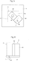
- FIG. 5 is a plan view of the illuminating device 1.
- FIG. 5 there is illustrated a state in which the light source holder 6 is removed.
- a recess 20 for positioning the slide glass 2 is formed, and the opening 40 is opened at the center of the recess 20.
- refractive index matching liquid for example, oil for oil immersion may be applied by drops between the slide glass 2 and the device substrate 4.
- a holder fixing seat 60 is formed adjacent to the recess in the top surface 4a of the device substrate, and the light source holder 6 is screwed onto the holder fixing seat 60.
- This holder fixing seat 60 is located immediately above the incident reflecting surface 7 formed on the device substrate 4, and when the laser light source 3 is held by the light source holder 6, the laser light L emitted from the laser light source 3 perpendicularly enters the top surface of the device substrate 4 such that the laser light L enters the incident reflecting surface 7 at a certain angle.
- the illuminating device 1 according to the present invention that was actually produced was formed by bonding the acrylic board for forming the device substrate 4 to the acrylic board for forming the support plate portion 5, and hence an introduction hole 65, which has a depth corresponding to a thickness of the acrylic board for forming the support plate portion 5, is formed in the holder fixing seat 60 such that the laser light L emitted from the laser light source 3 enters the device substrate 4 through the introduction hole 65. Therefore, when the support plate portion 5 and the device substrate 4 are formed of a single acrylic board, there is no need to form the introduction hole 65.
- FIG. 6 is a schematic view of the light source holder 6.
- This light source holder 6 includes a base portion 61, which is screwed onto the holder fixing seat 60, a light source holding portion 62, which is vertically erected from the base portion 61, and heat-radiating fins 63, which are formed integrally with the base portion 61 and the light source holding portion 62.
- a plurality of the heat-radiating fins 63 are arrayed along the paper depth direction of FIG. 6 .
- the laser light source 3 is fixed to the light source holding portion 62 such that the laser light L emitted thereby passes through a through hole 64, which is formed in the base portion 61, to enter the device substrate 4.
- the light source holder 6 is formed of a metal having good thermal conductivity, for example, aluminum, and the heat generated by the laser light source 3 is radiated into surrounding atmosphere by the heat-radiating fins 63.
- the laser light L emitted from the laser light source 3 is reflected by the incident reflecting surface 7 to enter the slide glass 2 at a predetermined angle, and is repeatedly and totally internally reflected in the slide glass 2 a plurality of times.
- the device substrate 4 being formed of the material having the refractive index at the same level as that of the slide glass 2
- the laser light L passes through an interface between the slide glass 2 and the device substrate 4 while being hardly refracted.
- the laser light L After being totally internally reflected at the front surface of the slide glass 2, the laser light L is totally internally reflected also on a back surface side of the slide glass 2 overlapping the opening 40.
- the laser light L is repeatedly and totally internally reflected in the slide glass 2 in the area in which the slide glass 2 overlaps the opening 40.
- the laser light L passes through the interface between the slide glass 2 and the device substrate 4 to enter the device substrate 4.
- the laser light source 3 when the laser light source 3 is held at a predetermined posture by the light source holder 6 fixed to the device substrate 4, and the laser light L is input to the incident reflecting surface 7 of the device substrate 4 at a predetermined angle, multiple total internal reflections naturally occur in the slide glass 2, and the evanescent wave Ev is generated at the area of the front surface of the slide glass 2 in which the total internal reflections occur.
- the evanescent wave can be generated easily and stably with no need for troublesome adjustment operations.
- the laser light that has entered the device substrate from the slide glass enters the exit reflecting surface is reflected in the direction that is parallel to the top surface of the device substrate and that does not interfere with the opening, and then is emitted from peripheral surfaces of the device substrate.
- Equipment of the microscope such as the objective lens and a revolving nosepiece for the objective lens exist below the microscope stage S, but when the laser light is emitted in the direction parallel to the top surface of the device substrate, in other words, a direction parallel to a front surface of the microscope stage as described above, the laser light can be prevented from being reflected by the equipment below the microscope stage and from generating scattered light, which is hard to predict. As a result, good fluorescence observation with a high S/N ratio can be performed.
- the total internal reflection sample illuminating device when the total internal reflection sample illuminating device according to the present invention is placed on the stage of the microscope, the evanescent wave can be generated easily and stably, and the observation of an object by a total internal reflection fluorescence microscope using the evanescent wave is facilitated.
- the total internal reflection sample illuminating device is therefore expected to become popular in a variety of fields, such as biology, medicine, and environment.
- the total internal reflection sample illuminating device according to the present invention which generates the evanescent wave easily and stably, is also effective in measurement using totally internally reflected Raman scattered light with the evanescent wave being excitation light, and the measurement enables non-invasive measurement in the vicinity of the interface.
- the total internal reflection sample illuminating device is expected to be used in the variety of fields, such as biology, medicine, and environment.
Landscapes
- Physics & Mathematics (AREA)
- Health & Medical Sciences (AREA)
- Analytical Chemistry (AREA)
- General Physics & Mathematics (AREA)
- Chemical & Material Sciences (AREA)
- Biochemistry (AREA)
- Life Sciences & Earth Sciences (AREA)
- General Health & Medical Sciences (AREA)
- Immunology (AREA)
- Pathology (AREA)
- Nuclear Medicine, Radiotherapy & Molecular Imaging (AREA)
- Optics & Photonics (AREA)
- Investigating, Analyzing Materials By Fluorescence Or Luminescence (AREA)
- Investigating Or Analysing Materials By Optical Means (AREA)
Abstract
Description
- The present invention relates to a total internal reflection sample illuminating device, which is configured to generate an evanescent wave as excitation light in fluorescence observation with a microscope and measurement using totally internally reflected Raman scattered light, for example.
- As a method of observing and measuring only the close vicinity of an interface of a sample, there has been known fluorescence observation using an evanescent wave as local excitation light. The evanescent wave is light that seeps out, when light enters an interface between two substances having different refractive indices from the side of the substance having the larger refractive index at a critical angle or more, and is totally internally reflected by the interface, to the side of the substance having the smaller refractive index. The evanescent wave has an intensity that decays exponentially as travelling away from the total internal reflection interface. Therefore, in the fluorescence observation using such evanescent wave, a fluorescent dye that exists at a distance of about 100 nm from the total internal reflection interface can be selectively excited, and observation and measurement specialized only in a shallow region in the close vicinity of the interface can be achieved.
- In the related art, as a total internal reflection sample illuminating device configured to perform irradiation with the evanescent wave, there has been known a total internal reflection sample illuminating device disclosed in
Patent Literature 1. This device includes an incident prism, which is fixed to a laser light source, and a radiation prism, which is supported to be adjustable in position in a direction of approaching the incident prism. The device is configured to support both ends of a slide glass, on which a sample is placed, from below by the incident prism and the radiation prism described above. Laser light emitted from the laser light source is guided into the slide glass through a contact surface between the incident prism and the slide glass, and after being repeatedly and totally internally reflected in the slide glass a plurality of times, is guided into the radiation prism from the contact surface between the slide glass and the radiation prism to be emitted from the radiation prism to the outside. - When the laser light is totally internally reflected in the slide glass, evanescent waves are generated at a front surface of the slide glass to correspond to positions at which the laser light is totally internally reflected. The fluorescent dye in the sample is excited by being irradiated with the evanescent waves only in the close vicinity of the front surface of the slide glass, and the excitation light can be observed with an objective lens arranged below the slide glass.
- Moreover, in recent years, there has also been proposed a technology of non-invasively measuring the vicinity of the interface by capturing the totally internally reflected Raman scattered light generated from the sample using the evanescent wave as the excitation light and without using the fluorescent dye (Non Patent Literature 1), and application of the total internal reflection sample illuminating device, which is configured to generate the evanescent wave, is expected in a variety of fields, such as biology, medicine, and environment.
- [PTL 1]
JP 2007-85915 A - [NPL 1] Kuriyama. R, Tateishi. T, Sato. Y, "Development of Total Internal Reflection Raman Imaging for Non-intrusive Quantitative Visualization of Near-wall Concentration", 17th International Symposium on Applications of Laser Techniques to Fluid Mechanics, 2014
- However, with such total internal reflection illuminating device in the related art, when an angle of incidence of the laser light that enters the slide glass through the incident prism is different by 1°, a magnitude and an intensity of the evanescent wave generated at the front surface of the slide glass are changed, and hence skill in the art has been required for adjusting a positional relationship between the laser light source and the incident prism. Moreover, unless a position of the radiation prism is optimally adjusted, the laser light radiated from the radiation prism to the outside generates scattered light, and the scattered light becomes a factor in a reduction of an SN ratio during the observation and measurement. In addition, when the positional relationship between the laser light source and the incident prism is adjusted, adjustment of the position of the radiation prism is also required accordingly, and there has been a problem in that handling of the device has been troublesome.
- The present invention has been made in view of the above-mentioned problems, and therefore has an object to provide a total internal reflection sample illuminating device, which is capable of generating an evanescent wave easily only through inputting laser light without skill in the art, and which is easy to handle in performing observation and measurement.
- That is, according to one embodiment of the present invention, there is provided a total internal reflection sample illuminating device, which is configured to introduce laser light into a slide glass such that the laser light undergoes multiple total internal reflections in the slide glass to generate an evanescent wave at a top surface of the slide glass, and to illuminate a sample, which is positioned on the top surface of the slide glass, with the evanescent wave, the total internal reflection sample illuminating device including a device substrate, which is formed of a material having a refractive index at the same level as a refractive index of the slide glass.
- An opening is formed to pierce between a top surface and a bottom surface of the device substrate, and the slide glass can be placed on the top surface so as to block the opening. Moreover, a light source holder, which is configured to hold a laser light source, is fixed to the top surface of the device substrate, and to allow laser light emitted by the laser light source to enter the top surface of the device substrate at a predetermined angle. An incident reflecting surface is formed on the bottom surface side of the device substrate. The laser light that has entered the device substrate from the laser light source is reflected by the incident reflecting surface to enter the slide glass, and to undergo multiple total internal reflections in an area of the slide glass that overlaps the opening. As a result, the evanescent wave is generated at a front surface of the slide glass to correspond to the area in which the laser light is totally internally reflected, and the sample on the slide glass can be illuminated with the evanescent wave. Meanwhile, on the bottom surface side of the device substrate, an exit reflecting surface is formed in an area opposed to the incident reflecting surface across the opening. This exit reflecting surface is configured to reflect the laser light that has entered the device substrate from the slide glass in a direction that is parallel to the top surface of the device main body and that does not interfere with the opening, and to emit the laser light to the outside of the device substrate.
- According to the present invention described above, the incident reflecting surface is formed on the device substrate, and the light source holder, which is configured to hold the laser light source, is fixed to the device substrate. Therefore, the angle of incidence of a laser beam with respect to the incident reflecting surface is always constant, and with the slide glass being placed on the device substrate, the relationship between the slide glass and the incident reflecting surface also is constant. Further, for the device substrate, there is used a material having a refractive index at the same level as that of the slide glass. Therefore, there is almost no need to consider refraction of the laser light at a boundary surface between the slide glass and the device substrate, and the total internal reflection of the laser light in the slide glass occurs only at the front surface of the slide glass, on which the sample is placed, and a back surface of the slide glass facing the opening. As a result, only through setting, to the device substrate, the slide glass and the light source holder holding the laser light source, the angle of incidence of the laser light with respect to the slide glass becomes always constant, and the evanescent wave can be stably generated only in the area in which the slide glass overlaps the opening of the device substrate. In addition, the evanescent wave can be generated easily with no need for troublesome adjustment operations.
- Moreover, the laser light that has entered the device substrate from the slide glass after the evanescent wave is generated is reflected by the exit reflecting surface, which is formed on the device substrate, in a direction that is parallel to the front surface of the device substrate and that does not interfere with the opening, and is then emitted from the device substrate. As a result, scattered light is not generated by the laser light being reflected by the objective lens, which is located below a stage of a microscope or the like, a revolving nosepiece for the objective lens, and other such devices, and good observation and measurement with a high S/N ratio can be performed.
- As long as having the opening, which induces the total internal reflection of the laser light, substantially at the center and being formed into a plate shape, the device substrate may have any external shape. However, from a viewpoint of facilitating formation of the incident reflecting surface and the exit reflecting surface, it is preferred that the device substrate be formed into a rectangular shape. With the device substrate being formed into the rectangular shape, the incident reflecting surface and the exit reflecting surface can be formed in a pair of corner portions across the opening by cutting off the corner portions obliquely.
- Moreover, the total internal reflection sample illuminating device according to the present invention is used by being placed on a stage of an inverted microscope or a stage of various kinds of measurement hardware, for example. However, from a viewpoint of making the device easily fixable to the stage for the use, it is preferred to form a support plate portion, which is to be placed on the stage, on a periphery of the top surface side of the device substrate, and to form a boss, which is used to position the device substrate in a hole in the stage, on a back surface side of the support plate portion. With this configuration, only through placing the device according to the present invention on the stage, the objective lens of the microscope can be positioned with respect to the opening of the device substrate, for example, and the observation using the evanescent wave can be started easily.
- As a material of the device substrate, a material having a refractive index at the same level as that of the slide glass, having high transparency, and not showing autofluorescence is preferred, and a plate material made of a clear colorless acrylic resin (hereinafter referred to as "acrylic board") may be used, for example. In that case, the incident reflecting surface and the exit reflecting surface may be formed by directly evaporating a metallic thin film onto the acrylic board for forming the device substrate. However, an acrylic board having one surface onto which a metallic thin film is evaporated (hereinafter referred to as "acrylic mirror board") is commercially available, and hence the device substrate may be formed by bonding the acrylic mirror board to a clear colorless acrylic board. In this manner, the device substrate may be produced inexpensively.
-
-
FIG. 1 is a schematic view for illustrating an example of a total internal reflection sample illuminating device to which an embodiment of the present invention is applied. -
FIG. 2 is a bottom view for illustrating the total internal reflection sample illuminating device according to the embodiment. -
FIG. 3 is a front view for illustrating the total internal reflection sample illuminating device according to the embodiment. -
FIG. 4 is a back view for illustrating the total internal reflection sample illuminating device according to the embodiment. -
FIG. 5 is a plan view for illustrating the total internal reflection sample illuminating device according to the embodiment. -
FIG. 6 is a side view for illustrating a light source holder of the total internal reflection sample illuminating device according to the embodiment. - Now, with reference to the accompanying drawings, description is made of a total internal reflection sample illuminating device to which an embodiment of the present invention is applied.
-
FIG. 1 is a cross-sectional view for schematically illustrating a total internal reflection sample illuminating device (hereinafter referred to as "illuminating device") to which the present invention is applied. Thisilluminating device 1 is used by being placed on a stage S of an inverted fluorescence microscope, for example, and when aslide glass 2 is set at a predetermined position of theilluminating device 1, and laser light L is emitted from alaser light source 3 fixed to theilluminating device 1, an evanescent wave Ev is generated at a predetermined position of a front surface of theslide glass 2. Therefore, when theslide glass 2, on which a sample containing a fluorescent dye is placed, is set to theilluminating device 1, the fluorescent dye in the sample is excited with the evanescent wave Ev that has seeped out on the front surface of theslide glass 2, and fluorescence observation may be performed on the sample with an objective lens R from below the microscope stage S through theslide glass 2. - The illuminating
device 1 includes adevice substrate 4, which is arranged in a hole in the microscope stage S, and which has anopening 40 for the objective lens R substantially at the center, asupport plate portion 5, which extends on a periphery of the top surface side of thedevice substrate 4 to be overlaid on the microscope stage S, and alight source holder 6, which is fixed to atop surface 4a of thedevice substrate 4 to hold thelaser light source 3. Moreover, thedevice substrate 4 has formed thereon anincident reflecting surface 7, which is configured to reflect, toward theslide glass 2, the laser light L that has entered thedevice substrate 4 from thelaser light source 3, and anexit reflecting surface 8, which is configured to reflect the laser light L that has entered thedevice substrate 4 from theslide glass 2, and to emit the laser light L from thedevice substrate 4 to the outside. - The
support plate portion 5 and thedevice substrate 4 are formed integrally, and thelight source holder 6 is fixed to the top surface of thedevice substrate 4 with screws. Moreover, on a lower surface side of thesupport plate portion 5 on the periphery of thedevice substrate 4, aboss 9 to be fitted into the hole in the microscope stage S is formed. When thesupport plate portion 5 is placed on the microscope stage S such that theboss 9 is fitted into the hole, theopening 40 formed in thedevice substrate 4 is positioned at the center of the hole in the microscope stage S, and the objective lens R of the microscope is positioned in theopening 40. - The
device substrate 4 needs to be formed of a material having a refractive index at the same level as that of theslide glass 2, having high transparency, and not showing autofluorescence for a wavelength of the laser light L to be used, and the same material as that of theslide glass 2 for observation may be used, for example. In this embodiment, there is used an acrylic board, which is easily processed, for example, cut or bonded, and which is available inexpensively as compared to a glass plate. -
FIG. 2 to FIG. 4 are a bottom view, a front view, and a back view for illustrating details of a shape of the illuminatingdevice 1, respectively. InFIG. 2 to FIG. 4 , there is illustrated a state in which thelight source holder 6 is removed from thedevice substrate 4. Thesupport plate portion 5 is formed into a quadrangular shape, and has a bottom surface in which theboss 9 is formed into a substantially circular shape at the center. A shape of theboss 9 matches a shape of the hole in the microscope stage S, and is different for a manufacturer of the microscope. Moreover, on a bottom surface of theboss 9, thedevice substrate 4 projects into a substantially rectangular shape. Theopening 40 is located at the center of theboss 9 to pierce between the top surface and the bottom surface of thedevice substrate 4, but exists at a position slightly deviated from the center of thedevice substrate 4. - There are four corner portions on the bottom surface side of the
device substrate 4, which is formed into the rectangular shape, and on two corner portions located diagonally across theopening 40, theincident reflecting surface 7 and theexit reflecting surface 8 are located. Theincident reflecting surface 7 and theexit reflecting surface 8 are formed as inclined surfaces obtained by cutting off the corner portions on the bottom surface side of thedevice substrate 4 obliquely at a predetermined angle, and may be formed by evaporating a metallic thin film made of aluminum or the like onto the inclined surfaces. - In the illuminating
device 1 according to the present invention that was actually produced by the inventors of the present invention, in order to suppress production cost, a commercially available acrylic mirror board was used for theincident reflecting surface 7 and theexit reflecting surface 8, and the acrylic mirror board was bonded to the above-mentioned acrylic board, to thereby form theincident reflecting surface 7 and theexit reflecting surface 8 on thedevice substrate 4. Thesupport plate portion 5, theboss 9, and thedevice substrate 4 were also formed into a predetermined shape by bonding acrylic boards having different thicknesses. Bonded surfaces were mirror-polished, and a UV-curable resin was used as an adhesive to prevent minute cracks and air bubbles from being incorporated between the surfaces of the acrylic boards during bonding. Moreover, a surface roughness of a surface on the periphery of thedevice substrate 4, which is formed into the substantially rectangular shape, was designed to be Ra=0.05 or less. - As illustrated in the plan view of
FIG. 2 , theincident reflecting surface 7 reflects the laser light L that has entered from the top surface of thedevice substrate 4 toward a center direction of theopening 40, and theexit reflecting surface 8 exists beyond theopening 40. In reality, the laser light L does not travel straight from theincident reflecting surface 7 to theexit reflecting surface 8, but as illustrated inFIG. 1 , enters theslide glass 2 obliquely from below, passes through theslide glass 2 while being repeatedly and totally internally reflected, and then enters theexit reflecting surface 8. Theexit reflecting surface 8 reflects the laser light L vertically in a direction that is parallel to the top surface of thedevice substrate 4 as illustrated inFIG. 1 , but reflects the laser light L horizontally not back in a direction of theincident reflecting surface 7, but in a direction in which an angle α is formed with the incident laser light L as illustrated inFIG. 2 . As a result, the laser light L is prevented from interfering with theopening 40 for the objective lens R. -
FIG. 5 is a plan view of the illuminatingdevice 1. InFIG. 5 , there is illustrated a state in which thelight source holder 6 is removed. At the center of thetop surface 4a of thedevice substrate 4, arecess 20 for positioning theslide glass 2 is formed, and theopening 40 is opened at the center of therecess 20. When theslide glass 2 is placed in therecess 20, refractive index matching liquid, for example, oil for oil immersion may be applied by drops between theslide glass 2 and thedevice substrate 4. Moreover, aholder fixing seat 60 is formed adjacent to the recess in thetop surface 4a of the device substrate, and thelight source holder 6 is screwed onto theholder fixing seat 60. Thisholder fixing seat 60 is located immediately above theincident reflecting surface 7 formed on thedevice substrate 4, and when thelaser light source 3 is held by thelight source holder 6, the laser light L emitted from thelaser light source 3 perpendicularly enters the top surface of thedevice substrate 4 such that the laser light L enters theincident reflecting surface 7 at a certain angle. - The illuminating
device 1 according to the present invention that was actually produced was formed by bonding the acrylic board for forming thedevice substrate 4 to the acrylic board for forming thesupport plate portion 5, and hence anintroduction hole 65, which has a depth corresponding to a thickness of the acrylic board for forming thesupport plate portion 5, is formed in theholder fixing seat 60 such that the laser light L emitted from thelaser light source 3 enters thedevice substrate 4 through theintroduction hole 65. Therefore, when thesupport plate portion 5 and thedevice substrate 4 are formed of a single acrylic board, there is no need to form theintroduction hole 65. -
FIG. 6 is a schematic view of thelight source holder 6. Thislight source holder 6 includes abase portion 61, which is screwed onto theholder fixing seat 60, a lightsource holding portion 62, which is vertically erected from thebase portion 61, and heat-radiatingfins 63, which are formed integrally with thebase portion 61 and the lightsource holding portion 62. A plurality of the heat-radiatingfins 63 are arrayed along the paper depth direction ofFIG. 6 . Thelaser light source 3 is fixed to the lightsource holding portion 62 such that the laser light L emitted thereby passes through a throughhole 64, which is formed in thebase portion 61, to enter thedevice substrate 4. Moreover, in order to prevent thelaser light source 3 from overheating while emitting the laser light L, and the heat from being conducted to thedevice substrate 4, thelight source holder 6 is formed of a metal having good thermal conductivity, for example, aluminum, and the heat generated by thelaser light source 3 is radiated into surrounding atmosphere by the heat-radiatingfins 63. - In the illuminating device configured as described above, as illustrated in
FIG. 1 , the laser light L emitted from thelaser light source 3 is reflected by theincident reflecting surface 7 to enter theslide glass 2 at a predetermined angle, and is repeatedly and totally internally reflected in the slide glass 2 a plurality of times. With thedevice substrate 4 being formed of the material having the refractive index at the same level as that of theslide glass 2, the laser light L passes through an interface between theslide glass 2 and thedevice substrate 4 while being hardly refracted. After being totally internally reflected at the front surface of theslide glass 2, the laser light L is totally internally reflected also on a back surface side of theslide glass 2 overlapping theopening 40. Then, the laser light L is repeatedly and totally internally reflected in theslide glass 2 in the area in which theslide glass 2 overlaps theopening 40. When arriving at a portion in which theslide glass 2 and thedevice substrate 4 overlap, the laser light L passes through the interface between theslide glass 2 and thedevice substrate 4 to enter thedevice substrate 4. - Therefore, when the
laser light source 3 is held at a predetermined posture by thelight source holder 6 fixed to thedevice substrate 4, and the laser light L is input to theincident reflecting surface 7 of thedevice substrate 4 at a predetermined angle, multiple total internal reflections naturally occur in theslide glass 2, and the evanescent wave Ev is generated at the area of the front surface of theslide glass 2 in which the total internal reflections occur. As a result, the evanescent wave can be generated easily and stably with no need for troublesome adjustment operations. - Meanwhile, the laser light that has entered the device substrate from the slide glass enters the exit reflecting surface, is reflected in the direction that is parallel to the top surface of the device substrate and that does not interfere with the opening, and then is emitted from peripheral surfaces of the device substrate. Equipment of the microscope, such as the objective lens and a revolving nosepiece for the objective lens exist below the microscope stage S, but when the laser light is emitted in the direction parallel to the top surface of the device substrate, in other words, a direction parallel to a front surface of the microscope stage as described above, the laser light can be prevented from being reflected by the equipment below the microscope stage and from generating scattered light, which is hard to predict. As a result, good fluorescence observation with a high S/N ratio can be performed.
- As described above, when the total internal reflection sample illuminating device according to the present invention is placed on the stage of the microscope, the evanescent wave can be generated easily and stably, and the observation of an object by a total internal reflection fluorescence microscope using the evanescent wave is facilitated. The total internal reflection sample illuminating device is therefore expected to become popular in a variety of fields, such as biology, medicine, and environment.
- Moreover, the total internal reflection sample illuminating device according to the present invention, which generates the evanescent wave easily and stably, is also effective in measurement using totally internally reflected Raman scattered light with the evanescent wave being excitation light, and the measurement enables non-invasive measurement in the vicinity of the interface. As a result, the total internal reflection sample illuminating device is expected to be used in the variety of fields, such as biology, medicine, and environment.
Claims (4)
- A total internal reflection sample illuminating device, which is configured to introduce laser light into a slide glass (2) such that the laser light undergoes multiple total internal reflections in the slide glass to generate an evanescent wave at a top surface of the slide glass, and to illuminate a sample, which is positioned on the top surface of the slide glass, with the evanescent wave, the total internal reflection sample illuminating device comprising:a device substrate (4), which is formed of a material having a refractive index at the same level as a refractive index of the slide glass (2), and which has an opening (40) formed to pierce between a top surface and a bottom surface of the device substrate, and has the slide glass placed on the top surface so as to block the opening;a light source holder (6), which is fixed to the top surface of the device substrate (4) to hold a laser light source (3), and which is configured to allow laser light emitted by the laser light source to enter the top surface of the device substrate at a predetermined angle;an incident reflecting surface (7), which is formed on the bottom surface side of the device substrate (4), and which is configured to reflect the laser light that has entered the device substrate (4) from the laser light source (3) such that the laser light enters the slide glass (2) and undergoes multiple total internal reflections in an area of the slide glass (2) that overlaps the opening (40); andan exit reflecting surface (8), which is formed on the bottom surface side of the device substrate (4), and in an area opposed to the incident reflecting surface (7) across the opening (40), and which is configured to reflect the laser light that has entered the device substrate (4) from the slide glass (2) in a direction that is parallel to the top surface of the device substrate (4) and that does not interfere with the opening (40).
- A total internal reflection sample illuminating device according to claim 1, wherein the device substrate (4) is formed into a rectangular shape, and the incident reflecting surface (7) and the exit reflecting surface (8) are formed in a pair of corner portions across the opening (40).
- A total internal reflection sample illuminating device according to claim 1 or 2, further comprising:a support plate portion (5), which is formed on a periphery of the top surface side of the device substrate (4), and which is placed on an observation stage; anda boss (9), which is formed on the support plate portion (5) to position the device substrate (4) in a hole in the observation stage.
- A total internal reflection sample illuminating device according to any one of claims 1 to 3, wherein the device substrate (4) is formed by bonding an acrylic board, onto which a metallic thin film is evaporated, and which is to form the incident reflecting surface (7) and the exit reflecting surface (8), to another clear colorless acrylic board.
Applications Claiming Priority (2)
| Application Number | Priority Date | Filing Date | Title |
|---|---|---|---|
| JP2015038153A JP6062980B2 (en) | 2015-02-27 | 2015-02-27 | Total reflection sample illumination system |
| PCT/JP2016/055789 WO2016136937A1 (en) | 2015-02-27 | 2016-02-26 | Total internal reflection sample illuminating device |
Publications (3)
| Publication Number | Publication Date |
|---|---|
| EP3264069A1 true EP3264069A1 (en) | 2018-01-03 |
| EP3264069A4 EP3264069A4 (en) | 2018-06-06 |
| EP3264069B1 EP3264069B1 (en) | 2019-05-22 |
Family
ID=56788762
Family Applications (1)
| Application Number | Title | Priority Date | Filing Date |
|---|---|---|---|
| EP16755681.0A Active EP3264069B1 (en) | 2015-02-27 | 2016-02-26 | Total internal reflection sample illuminating device |
Country Status (3)
| Country | Link |
|---|---|
| EP (1) | EP3264069B1 (en) |
| JP (1) | JP6062980B2 (en) |
| WO (1) | WO2016136937A1 (en) |
Families Citing this family (2)
| Publication number | Priority date | Publication date | Assignee | Title |
|---|---|---|---|---|
| CN113758901B (en) * | 2020-06-04 | 2024-04-12 | 中国科学院苏州纳米技术与纳米仿生研究所 | Diffraction tomography microscopic imaging system and method |
| CN115097617B (en) * | 2022-07-15 | 2022-12-30 | 中国科学技术大学 | Total internal reflection fluorescence microscope system based on planar chip |
Family Cites Families (10)
| Publication number | Priority date | Publication date | Assignee | Title |
|---|---|---|---|---|
| WO1992019976A1 (en) * | 1991-04-26 | 1992-11-12 | Gesellschaft Zur Förderung Der Industrieorientierten Forschung An Den Schweizerischen Hochschulen Und Weiteren Institutionen | Process and device for determining measured quantities by means of an integrated optical sensor module |
| JP3368477B2 (en) * | 1992-06-26 | 2003-01-20 | 日水製薬株式会社 | Optical measuring device |
| DE10217098B4 (en) * | 2002-04-17 | 2004-04-15 | Carl Zeiss Jena Gmbh | Incident lighting arrangement for a microscope |
| JP2006153643A (en) * | 2004-11-29 | 2006-06-15 | Toshiba Corp | measuring device |
| DE102005040833A1 (en) * | 2005-08-25 | 2007-03-08 | Carl Zeiss Jena Gmbh | TIRF-type microscope optical arrangement, has illumination light carried in beam paths outside microscope objective |
| WO2007034796A1 (en) * | 2005-09-26 | 2007-03-29 | National University Corporation Hamamatsu University School Of Medicine | Microscope cell observing/inspecting system using a plurality of observation techniques |
| EP2003441B1 (en) * | 2007-06-13 | 2011-01-05 | Mettler-Toledo AG | ATR sensor |
| JP2009123633A (en) * | 2007-11-19 | 2009-06-04 | Central Glass Co Ltd | Evanescent light source |
| JP5877942B2 (en) * | 2010-11-29 | 2016-03-08 | 浜松ホトニクス株式会社 | Total reflection spectrometer |
| CN102323218A (en) * | 2011-05-26 | 2012-01-18 | 浙江大学 | Material real-time detection monitoring device on basis of spectrum technology |
-
2015
- 2015-02-27 JP JP2015038153A patent/JP6062980B2/en active Active
-
2016
- 2016-02-26 WO PCT/JP2016/055789 patent/WO2016136937A1/en not_active Ceased
- 2016-02-26 EP EP16755681.0A patent/EP3264069B1/en active Active
Also Published As
| Publication number | Publication date |
|---|---|
| WO2016136937A1 (en) | 2016-09-01 |
| EP3264069A4 (en) | 2018-06-06 |
| JP2016161319A (en) | 2016-09-05 |
| EP3264069B1 (en) | 2019-05-22 |
| JP6062980B2 (en) | 2017-01-18 |
Similar Documents
| Publication | Publication Date | Title |
|---|---|---|
| CN103033497B (en) | Microfluidic chip analyzer applying raman spectrum for detection | |
| US20200003688A1 (en) | Surface Plasmon Resonance Fluorescence Analysis Device And Surface Plasmon Resonance Fluorescence Analysis Method | |
| EP3064929B1 (en) | Surface plasmon resonance fluorescence analysis method and surface plasmon resonance fluorescence analysis device | |
| US8102533B2 (en) | Total reflection illuminated sensor chip | |
| EP2513628A1 (en) | Methods and systems for optical characterisation | |
| CN116577317A (en) | Combined detection device and combined detection method for Raman-laser ablation-mass spectrum | |
| CN102348406A (en) | Optical probe for measuring light signals in vivo | |
| EP3153845A1 (en) | Surface-plasmon enhanced fluorescence measurement method, surface-plasmon enhanced fluorescence measurement device, and analytical chip | |
| US20250341712A1 (en) | Apparatuses, systems and methods for solid immersion meniscus lenses | |
| WO2018021238A1 (en) | Detection chip, detection system, and detection method | |
| JP6587024B2 (en) | Detection method and detection apparatus | |
| EP3264069B1 (en) | Total internal reflection sample illuminating device | |
| US20170343580A1 (en) | Scanning probe microscope and sample holder therefor | |
| JP5107003B2 (en) | Evanescent wave generator and observation apparatus using the same | |
| JP6766820B2 (en) | Optical sample detection system | |
| Waldauer et al. | Microfluidic mixers for studying protein folding | |
| EP2228637A1 (en) | Total reflection illuminated sensor chip, method for producing the total reflection illuminated sensor chip, and sensing method using the total reflection illuminated sensor chip | |
| EP3159677A1 (en) | Detection device | |
| JP6588055B2 (en) | Bacteria detection device | |
| US20170336612A1 (en) | Inhomogeneous Surface Wave Microscope | |
| US9791375B2 (en) | Light measuring apparatus employing optical electric field enhancing device | |
| KR20090007172A (en) | Plate glass thickness measuring device | |
| JP6586884B2 (en) | Chip and surface plasmon enhanced fluorescence measurement method | |
| JP2002357544A (en) | measuring device | |
| KR101247661B1 (en) | Cross section inspection member using total reflection pattern and cross section inspection method thereof |
Legal Events
| Date | Code | Title | Description |
|---|---|---|---|
| STAA | Information on the status of an ep patent application or granted ep patent |
Free format text: STATUS: THE INTERNATIONAL PUBLICATION HAS BEEN MADE |
|
| PUAI | Public reference made under article 153(3) epc to a published international application that has entered the european phase |
Free format text: ORIGINAL CODE: 0009012 |
|
| STAA | Information on the status of an ep patent application or granted ep patent |
Free format text: STATUS: REQUEST FOR EXAMINATION WAS MADE |
|
| 17P | Request for examination filed |
Effective date: 20170908 |
|
| AK | Designated contracting states |
Kind code of ref document: A1 Designated state(s): AL AT BE BG CH CY CZ DE DK EE ES FI FR GB GR HR HU IE IS IT LI LT LU LV MC MK MT NL NO PL PT RO RS SE SI SK SM TR |
|
| AX | Request for extension of the european patent |
Extension state: BA ME |
|
| A4 | Supplementary search report drawn up and despatched |
Effective date: 20180504 |
|
| DAV | Request for validation of the european patent (deleted) | ||
| DAX | Request for extension of the european patent (deleted) | ||
| RIC1 | Information provided on ipc code assigned before grant |
Ipc: G01N 21/01 20060101ALI20180427BHEP Ipc: G01N 21/64 20060101AFI20180427BHEP Ipc: G02B 21/06 20060101ALI20180427BHEP Ipc: G01N 21/65 20060101ALI20180427BHEP Ipc: G02B 21/00 20060101ALI20180427BHEP |
|
| GRAP | Despatch of communication of intention to grant a patent |
Free format text: ORIGINAL CODE: EPIDOSNIGR1 |
|
| STAA | Information on the status of an ep patent application or granted ep patent |
Free format text: STATUS: GRANT OF PATENT IS INTENDED |
|
| RIC1 | Information provided on ipc code assigned before grant |
Ipc: G01N 21/64 20060101AFI20181126BHEP Ipc: G02B 21/00 20060101ALI20181126BHEP Ipc: G02B 21/10 20060101ALI20181126BHEP Ipc: G01N 21/65 20060101ALI20181126BHEP Ipc: G02B 21/06 20060101ALI20181126BHEP Ipc: G02B 21/16 20060101ALI20181126BHEP Ipc: G01N 21/01 20060101ALI20181126BHEP |
|
| INTG | Intention to grant announced |
Effective date: 20181218 |
|
| GRAS | Grant fee paid |
Free format text: ORIGINAL CODE: EPIDOSNIGR3 |
|
| GRAA | (expected) grant |
Free format text: ORIGINAL CODE: 0009210 |
|
| STAA | Information on the status of an ep patent application or granted ep patent |
Free format text: STATUS: THE PATENT HAS BEEN GRANTED |
|
| AK | Designated contracting states |
Kind code of ref document: B1 Designated state(s): AL AT BE BG CH CY CZ DE DK EE ES FI FR GB GR HR HU IE IS IT LI LT LU LV MC MK MT NL NO PL PT RO RS SE SI SK SM TR |
|
| REG | Reference to a national code |
Ref country code: GB Ref legal event code: FG4D |
|
| REG | Reference to a national code |
Ref country code: CH Ref legal event code: EP |
|
| REG | Reference to a national code |
Ref country code: IE Ref legal event code: FG4D |
|
| REG | Reference to a national code |
Ref country code: DE Ref legal event code: R096 Ref document number: 602016014404 Country of ref document: DE |
|
| REG | Reference to a national code |
Ref country code: AT Ref legal event code: REF Ref document number: 1136717 Country of ref document: AT Kind code of ref document: T Effective date: 20190615 |
|
| REG | Reference to a national code |
Ref country code: NL Ref legal event code: FP |
|
| REG | Reference to a national code |
Ref country code: LT Ref legal event code: MG4D |
|
| PG25 | Lapsed in a contracting state [announced via postgrant information from national office to epo] |
Ref country code: ES Free format text: LAPSE BECAUSE OF FAILURE TO SUBMIT A TRANSLATION OF THE DESCRIPTION OR TO PAY THE FEE WITHIN THE PRESCRIBED TIME-LIMIT Effective date: 20190522 Ref country code: LT Free format text: LAPSE BECAUSE OF FAILURE TO SUBMIT A TRANSLATION OF THE DESCRIPTION OR TO PAY THE FEE WITHIN THE PRESCRIBED TIME-LIMIT Effective date: 20190522 Ref country code: HR Free format text: LAPSE BECAUSE OF FAILURE TO SUBMIT A TRANSLATION OF THE DESCRIPTION OR TO PAY THE FEE WITHIN THE PRESCRIBED TIME-LIMIT Effective date: 20190522 Ref country code: SE Free format text: LAPSE BECAUSE OF FAILURE TO SUBMIT A TRANSLATION OF THE DESCRIPTION OR TO PAY THE FEE WITHIN THE PRESCRIBED TIME-LIMIT Effective date: 20190522 Ref country code: NO Free format text: LAPSE BECAUSE OF FAILURE TO SUBMIT A TRANSLATION OF THE DESCRIPTION OR TO PAY THE FEE WITHIN THE PRESCRIBED TIME-LIMIT Effective date: 20190822 Ref country code: FI Free format text: LAPSE BECAUSE OF FAILURE TO SUBMIT A TRANSLATION OF THE DESCRIPTION OR TO PAY THE FEE WITHIN THE PRESCRIBED TIME-LIMIT Effective date: 20190522 Ref country code: PT Free format text: LAPSE BECAUSE OF FAILURE TO SUBMIT A TRANSLATION OF THE DESCRIPTION OR TO PAY THE FEE WITHIN THE PRESCRIBED TIME-LIMIT Effective date: 20190922 Ref country code: AL Free format text: LAPSE BECAUSE OF FAILURE TO SUBMIT A TRANSLATION OF THE DESCRIPTION OR TO PAY THE FEE WITHIN THE PRESCRIBED TIME-LIMIT Effective date: 20190522 |
|
| PG25 | Lapsed in a contracting state [announced via postgrant information from national office to epo] |
Ref country code: RS Free format text: LAPSE BECAUSE OF FAILURE TO SUBMIT A TRANSLATION OF THE DESCRIPTION OR TO PAY THE FEE WITHIN THE PRESCRIBED TIME-LIMIT Effective date: 20190522 Ref country code: LV Free format text: LAPSE BECAUSE OF FAILURE TO SUBMIT A TRANSLATION OF THE DESCRIPTION OR TO PAY THE FEE WITHIN THE PRESCRIBED TIME-LIMIT Effective date: 20190522 Ref country code: GR Free format text: LAPSE BECAUSE OF FAILURE TO SUBMIT A TRANSLATION OF THE DESCRIPTION OR TO PAY THE FEE WITHIN THE PRESCRIBED TIME-LIMIT Effective date: 20190823 Ref country code: BG Free format text: LAPSE BECAUSE OF FAILURE TO SUBMIT A TRANSLATION OF THE DESCRIPTION OR TO PAY THE FEE WITHIN THE PRESCRIBED TIME-LIMIT Effective date: 20190822 |
|
| REG | Reference to a national code |
Ref country code: AT Ref legal event code: MK05 Ref document number: 1136717 Country of ref document: AT Kind code of ref document: T Effective date: 20190522 |
|
| PG25 | Lapsed in a contracting state [announced via postgrant information from national office to epo] |
Ref country code: CZ Free format text: LAPSE BECAUSE OF FAILURE TO SUBMIT A TRANSLATION OF THE DESCRIPTION OR TO PAY THE FEE WITHIN THE PRESCRIBED TIME-LIMIT Effective date: 20190522 Ref country code: SK Free format text: LAPSE BECAUSE OF FAILURE TO SUBMIT A TRANSLATION OF THE DESCRIPTION OR TO PAY THE FEE WITHIN THE PRESCRIBED TIME-LIMIT Effective date: 20190522 Ref country code: EE Free format text: LAPSE BECAUSE OF FAILURE TO SUBMIT A TRANSLATION OF THE DESCRIPTION OR TO PAY THE FEE WITHIN THE PRESCRIBED TIME-LIMIT Effective date: 20190522 Ref country code: DK Free format text: LAPSE BECAUSE OF FAILURE TO SUBMIT A TRANSLATION OF THE DESCRIPTION OR TO PAY THE FEE WITHIN THE PRESCRIBED TIME-LIMIT Effective date: 20190522 Ref country code: RO Free format text: LAPSE BECAUSE OF FAILURE TO SUBMIT A TRANSLATION OF THE DESCRIPTION OR TO PAY THE FEE WITHIN THE PRESCRIBED TIME-LIMIT Effective date: 20190522 Ref country code: AT Free format text: LAPSE BECAUSE OF FAILURE TO SUBMIT A TRANSLATION OF THE DESCRIPTION OR TO PAY THE FEE WITHIN THE PRESCRIBED TIME-LIMIT Effective date: 20190522 |
|
| REG | Reference to a national code |
Ref country code: DE Ref legal event code: R097 Ref document number: 602016014404 Country of ref document: DE |
|
| PG25 | Lapsed in a contracting state [announced via postgrant information from national office to epo] |
Ref country code: SM Free format text: LAPSE BECAUSE OF FAILURE TO SUBMIT A TRANSLATION OF THE DESCRIPTION OR TO PAY THE FEE WITHIN THE PRESCRIBED TIME-LIMIT Effective date: 20190522 Ref country code: IT Free format text: LAPSE BECAUSE OF FAILURE TO SUBMIT A TRANSLATION OF THE DESCRIPTION OR TO PAY THE FEE WITHIN THE PRESCRIBED TIME-LIMIT Effective date: 20190522 |
|
| PLBE | No opposition filed within time limit |
Free format text: ORIGINAL CODE: 0009261 |
|
| STAA | Information on the status of an ep patent application or granted ep patent |
Free format text: STATUS: NO OPPOSITION FILED WITHIN TIME LIMIT |
|
| PG25 | Lapsed in a contracting state [announced via postgrant information from national office to epo] |
Ref country code: TR Free format text: LAPSE BECAUSE OF FAILURE TO SUBMIT A TRANSLATION OF THE DESCRIPTION OR TO PAY THE FEE WITHIN THE PRESCRIBED TIME-LIMIT Effective date: 20190522 |
|
| 26N | No opposition filed |
Effective date: 20200225 |
|
| PG25 | Lapsed in a contracting state [announced via postgrant information from national office to epo] |
Ref country code: PL Free format text: LAPSE BECAUSE OF FAILURE TO SUBMIT A TRANSLATION OF THE DESCRIPTION OR TO PAY THE FEE WITHIN THE PRESCRIBED TIME-LIMIT Effective date: 20190522 |
|
| PG25 | Lapsed in a contracting state [announced via postgrant information from national office to epo] |
Ref country code: SI Free format text: LAPSE BECAUSE OF FAILURE TO SUBMIT A TRANSLATION OF THE DESCRIPTION OR TO PAY THE FEE WITHIN THE PRESCRIBED TIME-LIMIT Effective date: 20190522 |
|
| REG | Reference to a national code |
Ref country code: CH Ref legal event code: PL |
|
| GBPC | Gb: european patent ceased through non-payment of renewal fee |
Effective date: 20200226 |
|
| REG | Reference to a national code |
Ref country code: BE Ref legal event code: MM Effective date: 20200229 |
|
| PG25 | Lapsed in a contracting state [announced via postgrant information from national office to epo] |
Ref country code: MC Free format text: LAPSE BECAUSE OF FAILURE TO SUBMIT A TRANSLATION OF THE DESCRIPTION OR TO PAY THE FEE WITHIN THE PRESCRIBED TIME-LIMIT Effective date: 20190522 Ref country code: LU Free format text: LAPSE BECAUSE OF NON-PAYMENT OF DUE FEES Effective date: 20200226 |
|
| PG25 | Lapsed in a contracting state [announced via postgrant information from national office to epo] |
Ref country code: LI Free format text: LAPSE BECAUSE OF NON-PAYMENT OF DUE FEES Effective date: 20200229 Ref country code: CH Free format text: LAPSE BECAUSE OF NON-PAYMENT OF DUE FEES Effective date: 20200229 |
|
| PG25 | Lapsed in a contracting state [announced via postgrant information from national office to epo] |
Ref country code: IE Free format text: LAPSE BECAUSE OF NON-PAYMENT OF DUE FEES Effective date: 20200226 Ref country code: GB Free format text: LAPSE BECAUSE OF NON-PAYMENT OF DUE FEES Effective date: 20200226 |
|
| PG25 | Lapsed in a contracting state [announced via postgrant information from national office to epo] |
Ref country code: BE Free format text: LAPSE BECAUSE OF NON-PAYMENT OF DUE FEES Effective date: 20200229 |
|
| PGFP | Annual fee paid to national office [announced via postgrant information from national office to epo] |
Ref country code: DE Payment date: 20220217 Year of fee payment: 7 |
|
| PG25 | Lapsed in a contracting state [announced via postgrant information from national office to epo] |
Ref country code: MT Free format text: LAPSE BECAUSE OF FAILURE TO SUBMIT A TRANSLATION OF THE DESCRIPTION OR TO PAY THE FEE WITHIN THE PRESCRIBED TIME-LIMIT Effective date: 20190522 Ref country code: CY Free format text: LAPSE BECAUSE OF FAILURE TO SUBMIT A TRANSLATION OF THE DESCRIPTION OR TO PAY THE FEE WITHIN THE PRESCRIBED TIME-LIMIT Effective date: 20190522 |
|
| PGFP | Annual fee paid to national office [announced via postgrant information from national office to epo] |
Ref country code: NL Payment date: 20220216 Year of fee payment: 7 Ref country code: FR Payment date: 20220221 Year of fee payment: 7 |
|
| PG25 | Lapsed in a contracting state [announced via postgrant information from national office to epo] |
Ref country code: MK Free format text: LAPSE BECAUSE OF FAILURE TO SUBMIT A TRANSLATION OF THE DESCRIPTION OR TO PAY THE FEE WITHIN THE PRESCRIBED TIME-LIMIT Effective date: 20190522 Ref country code: IS Free format text: LAPSE BECAUSE OF FAILURE TO SUBMIT A TRANSLATION OF THE DESCRIPTION OR TO PAY THE FEE WITHIN THE PRESCRIBED TIME-LIMIT Effective date: 20190922 |
|
| REG | Reference to a national code |
Ref country code: DE Ref legal event code: R119 Ref document number: 602016014404 Country of ref document: DE |
|
| REG | Reference to a national code |
Ref country code: NL Ref legal event code: MM Effective date: 20230301 |
|
| PG25 | Lapsed in a contracting state [announced via postgrant information from national office to epo] |
Ref country code: NL Free format text: LAPSE BECAUSE OF NON-PAYMENT OF DUE FEES Effective date: 20230301 |
|
| PG25 | Lapsed in a contracting state [announced via postgrant information from national office to epo] |
Ref country code: FR Free format text: LAPSE BECAUSE OF NON-PAYMENT OF DUE FEES Effective date: 20230228 Ref country code: DE Free format text: LAPSE BECAUSE OF NON-PAYMENT OF DUE FEES Effective date: 20230901 |