EP3262742B1 - Electrostatic discharge protection and method in power supply - Google Patents
Electrostatic discharge protection and method in power supply Download PDFInfo
- Publication number
- EP3262742B1 EP3262742B1 EP15883563.7A EP15883563A EP3262742B1 EP 3262742 B1 EP3262742 B1 EP 3262742B1 EP 15883563 A EP15883563 A EP 15883563A EP 3262742 B1 EP3262742 B1 EP 3262742B1
- Authority
- EP
- European Patent Office
- Prior art keywords
- circuit
- power supply
- heat sink
- metal heat
- spark gap
- Prior art date
- Legal status (The legal status is an assumption and is not a legal conclusion. Google has not performed a legal analysis and makes no representation as to the accuracy of the status listed.)
- Active
Links
Images




Classifications
-
- H—ELECTRICITY
- H02—GENERATION; CONVERSION OR DISTRIBUTION OF ELECTRIC POWER
- H02H—EMERGENCY PROTECTIVE CIRCUIT ARRANGEMENTS
- H02H9/00—Emergency protective circuit arrangements for limiting excess current or voltage without disconnection
- H02H9/04—Emergency protective circuit arrangements for limiting excess current or voltage without disconnection responsive to excess voltage
- H02H9/045—Emergency protective circuit arrangements for limiting excess current or voltage without disconnection responsive to excess voltage adapted to a particular application and not provided for elsewhere
- H02H9/046—Emergency protective circuit arrangements for limiting excess current or voltage without disconnection responsive to excess voltage adapted to a particular application and not provided for elsewhere responsive to excess voltage appearing at terminals of integrated circuits
-
- H—ELECTRICITY
- H02—GENERATION; CONVERSION OR DISTRIBUTION OF ELECTRIC POWER
- H02M—APPARATUS FOR CONVERSION BETWEEN AC AND AC, BETWEEN AC AND DC, OR BETWEEN DC AND DC, AND FOR USE WITH MAINS OR SIMILAR POWER SUPPLY SYSTEMS; CONVERSION OF DC OR AC INPUT POWER INTO SURGE OUTPUT POWER; CONTROL OR REGULATION THEREOF
- H02M3/00—Conversion of DC power input into DC power output
- H02M3/22—Conversion of DC power input into DC power output with intermediate conversion into AC
- H02M3/24—Conversion of DC power input into DC power output with intermediate conversion into AC by static converters
- H02M3/28—Conversion of DC power input into DC power output with intermediate conversion into AC by static converters using discharge tubes with control electrode or semiconductor devices with control electrode to produce the intermediate AC
- H02M3/325—Conversion of DC power input into DC power output with intermediate conversion into AC by static converters using discharge tubes with control electrode or semiconductor devices with control electrode to produce the intermediate AC using devices of a triode or a transistor type requiring continuous application of a control signal
- H02M3/335—Conversion of DC power input into DC power output with intermediate conversion into AC by static converters using discharge tubes with control electrode or semiconductor devices with control electrode to produce the intermediate AC using devices of a triode or a transistor type requiring continuous application of a control signal using semiconductor devices only
- H02M3/33507—Conversion of DC power input into DC power output with intermediate conversion into AC by static converters using discharge tubes with control electrode or semiconductor devices with control electrode to produce the intermediate AC using devices of a triode or a transistor type requiring continuous application of a control signal using semiconductor devices only with automatic control of the output voltage or current, e.g. flyback converters
-
- H—ELECTRICITY
- H10—SEMICONDUCTOR DEVICES; ELECTRIC SOLID-STATE DEVICES NOT OTHERWISE PROVIDED FOR
- H10W—GENERIC PACKAGES, INTERCONNECTIONS, CONNECTORS OR OTHER CONSTRUCTIONAL DETAILS OF DEVICES COVERED BY CLASS H10
- H10W42/00—Arrangements for protection of devices
- H10W42/60—Arrangements for protection of devices protecting against electrostatic charges or discharges, e.g. Faraday shields
-
- H—ELECTRICITY
- H10—SEMICONDUCTOR DEVICES; ELECTRIC SOLID-STATE DEVICES NOT OTHERWISE PROVIDED FOR
- H10W—GENERIC PACKAGES, INTERCONNECTIONS, CONNECTORS OR OTHER CONSTRUCTIONAL DETAILS OF DEVICES COVERED BY CLASS H10
- H10W42/00—Arrangements for protection of devices
- H10W42/80—Arrangements for protection of devices protecting against overcurrent or overload, e.g. fuses or shunts
Definitions
- the present disclosure relates generally to power supplies for electrical and electronic equipment. More particularly the disclosure relates to protective circuit configurations to minimize the damaging effects of electrostatic discharges in power supplies and associated electronics to which those power supplies are coupled.
- the disclosed protective circuits are useful in a variety of applications and shown here in conjunction with electrically powered furniture such as lift chairs and recliners.
- Electrostatic discharge is a common and troublesome phenomena observed in dry conditions.
- the static generated can reach as high as 18 kv.
- This static electricity can travel from the person or furniture to electronic devices, particularly those having a power supply connected to an AC outlet.
- the outlet is grounded using a three-prong plug, the static discharge can usually be diverted around any delicate electronic components so that minimal damage is observed.
- the third prong is connected to an earth ground that acts as the least resistance path for discharge of the static electricity.
- the static discharge can run rampant through delicate electronic components, causing damage to the electronic device and its power supply.
- US-5892669A discloses a surge protecting circuit in which external energy surges arriving on the DC circuit are directed through the transformer to an arc discharge gap between the AC circuit and the AC ground. The majority of energy is dissipated thermally as a result of the discharge, with some feeding back into the AC input line. Such a system requires a grounded outlet.
- US-4586105A discloses a spark gap formation between adjacent conductive pathways on a printed circuit board designed to bypass individual sensitive electrical components such as semiconductor chips. US-4586105A does not relate specifically to surge protection in AC/DC transformers.
- US-6355958B1 discloses a spark gap assembly designed to improve thermal performance and heat dissipation after discharges, thus providing improved thermal protection for nearby sensitive components.
- EP-1612898B1 discloses a method for fabricating spark gap structures using laser ablation of conductive surfaces and discusses different geometries of spark gap structures. A shunt capacitor connected in parallel to the spark gap is used to provide extra protection and voltage limitation. EP-1612898B1 does not specifically relate to surge protection in AC/DC transformers.
- the spark gap or discharge pin(s) may be created on the printed circuit board, between the DC side and the AC side of the power supply.
- the structurally separated conductive surfaces can be made or created on the printed circuit board as well.
- the spark gap or the discharge pin(s) or conductive surfaces can be connected to the (+) positive terminal or the (-) negative terminal, or both; or to any other suitable reference point(s) on the DC side.
- the other side of the spark gap or discharge pin(s) or conductive surfaces are connected to the AC side, such as to the live (hot) terminal or the neutral terminal, or both; or to any other suitable reference point(s) on the AC side of the printed circuit board.
- the spark gap or discharge pin(s) or conductive surfaces can be any number of surfaces from one surface to any number of surfaces.
- the gap or distance between the spark gap or discharge pin(s) or conductive surfaces are adjusted to a minimum distance acceptable by the compliance agency for the separation between the AC and DC components. In this way the AC and DC sides of the power supply remain electrically isolated (AC line voltage does not flow to the DC side), yet electrostatic energy is conducted from the DC side to the AC side through a path that does not damage the electronic components of the power supply.
- a power supply for converting alternating current (AC) into direct current (DC) for powering a device.
- the power supply includes an AC circuit adapted for coupling to a source of alternating current and having a first common reference point (AC reference point) such an AC ground, an AC neutral or an AC hot terminal; and a DC circuit coupled to the AC circuit and providing direct current terminals for coupling to the powered device and having a second common reference point (DC reference point), such as a DC positive terminal, a DC negative terminal or a DC ground.
- the AC and DC grounds are electrically isolated to substantially inhibit the flow of direct current there between (and consequently to inhibit the flow of AC line voltage to the DC side).
- a first attachment point provides an energy pathway to the AC reference point, while a second attachment point provides an energy pathway to the DC reference point. In this way, damaging electrostatic charges are diverted around the delicate components of the power supply.
- a spark gap structure is coupled to the first and second attachment points. This spark gap structure is configured to substantially inhibit the flow of direct current between the first and second attachment points while providing a static electricity energy path between the first and second attachment points.
- the electrostatic discharge protection technique will be described here in connection with two typical use cases: a motorized chair that uses a DC power supply to energize the motors and controller circuits, and a laptop computer that uses a DC power supply to charge the internal battery and to provide operating power to the laptop.
- a motorized chair that uses a DC power supply to energize the motors and controller circuits
- a laptop computer that uses a DC power supply to charge the internal battery and to provide operating power to the laptop.
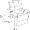
- Chair 10 is also exemplary of an electrically operated lift chair, a primary difference between recliner chairs and lift chairs being the respective range of motor assisted motions.
- Power to operate the motors and other electrical and electronic components of chair 10 is derived from a DC power supply 12 that is in turn coupled to a source of alternating (AC) current, such as an AC wall outlet 14.
- AC alternating
- Chair 10 may be provided with a controller 15, mounted on an arm of the chair.
- the controller 15 is powered by the power supply and provides control voltages that power internal motors (not shown) that adjust the seat back and leg rest portions of the chair.
- a detachable controller 16 may be provided.
- Controller 16 functions essentially the same as controller 15, but is attached to the internal electronic components via an umbilical cord as illustrated.
- the internal electronic components of the chair can include a radio circuit compatible with Bluetooth or WiFi protocols, to allow the char to be controlled remotely from a handheld portable device, such as a smartphone or tablet computer.
- Power supply 12 is preferably a switched mode power supply.
- Switched mode power supplies convert the standard 60 Hz. (or 50 Hz. in some locations) AC power into an alternating current of higher frequency. This is typically done with a solid state device such as a switching transistor. By converting the standard AC power to a higher frequency, much smaller step down transformers can be used, thus resulting in a much smaller and more convenient power supply package that is better suited for consumer applications. Once the voltage of this higher frequency alternating current has been stepped down to a voltage compatible with the DC motors and controller circuits, the lower voltage is rectified to convert it to the desired DC voltage.
- the switched mode power supply has an AC portion, on the primary side of the step down transformer, and a DC portion, on the secondary side of the step down transformer.
- FIG. 2 shows an exemplary switched mode power supply circuit in block diagram form.
- the power supply circuit includes an AC circuit portion 20 which is adapted for coupling to a source of alternating current as at AC input terminals 22. Terminals 22 are connected to a suitable power cord for connecting to an AC wall outlet.
- the power supply circuit also includes a DC circuit portion 24 having positive and negative DC terminals 26, which are then connected to the device being powered by the power supply.
- the power supply depicted in Figure 2 is exemplary of a switching mode power supply that includes an active switching component 28 that produces a switched alternating current at a frequency higher than the frequency of the source of alternating current supplied by the wall outlet.
- the DC circuit portion and AC circuit portion are coupled together through a transformer 30, which provides the line of demarcation between the AC circuit portion and the DC circuit portion.
- Transformer 30 is wound to act as a voltage step down transformer.
- a diode 32 for other suitable rectifier device converts the stepped-down voltage at the secondary side of transformer 30 into direct current which is then filtered by filter capacitors 34.
- a zener diode 36, or other suitable voltage regulating device, clamps the output DC voltage at the desired nominal operating voltage for the intended application.
- the active switching component 28 is driven by an electronic driver circuit 38.
- Circuit 38 forms part of a feedback circuit 40 that supplies control pulses to the active switching component 28 at the rate required to maintain the DC voltage output on terminals 26 at the desired voltage under different loads.
- the feedback circuit includes an optical coupler 42 which electrically isolates the DC circuit portion form the AC circuit portion
- the driver circuit 38 is powered by a DC supply voltage obtained using a bridge rectifier 44 and filter capacitor 46. It should be noted that the bridge rectifier 44 and filter capacitor 46 provide DC operating voltage to power the active switching component 28 and the driver circuit 38, although these components are on the AC circuit portion of the power supply.
- An electromagnetic interference (EMI) filter 48 is included across the line (L) and neutral (N) sides of the AC input terminals to protect the circuit from voltage surges and electrical noise entering the circuit through the AC power cord.
- EMI electromagnetic interference
- the AC circuit portion 20 has an AC ground designated by the AC ground symbol 50, which appears at numerous points within the AC circuit portion 20.
- the AC ground symbol 50 For example, one of the terminals of the bridge rectifier 44 is coupled to the AC ground as are a number of capacitors in the AC circuit potion.
- the active switching component 28 coupled to AC ground 50 through a bias resistor 52; and driver circuit 38 is likewise referenced to circuit ground at its ground pin 54.
- the DC circuit portion 24 has its own DC ground 56. A different symbol has been used for the DC ground to differentiate it from the AC ground in Figure 2 . Note that in the illustrated embodiment, the negative one of the DC terminals 26 is coupled to DC ground 56. It is also possible to construct a circuit with the opposite polarity, where the positive DC terminal is coupled to ground. Either option is possible depending on the requirements of the power device.
- FIG. 3 provides a more detailed circuit diagram of one embodiment of power supply. Where applicable, the same reference numerals as in Figure 2 have been used to designate like or comparable components. As discussed in connection with Figure 3 , transformer 30 generally defines the line of demarcation between the AC circuit portion 20 and DC circuit portion 24.
- Figure 4 shows how static electricity can be generated and find its way into delicate power supply circuits where significant damage can be done.
- a person seated in chair 10 holding laptop computer 70, slides forward to exit the chair.
- the person's posterior rubs against the fabric of the chair 11, which causes a separation of positive (+) and negative (-) charges as the cloth of the person's clothing rubs against the cloth or other material from which the chair is made.
- the chair fabric or other material are relatively poor conductors of electricity, a negative charge is stored in one material and a positive charge in the other.
- the person's clothing is shown as having a positive charge, while the fabric of the chair is shown as having a negative charge.
- the chair in Figure 4 becomes negatively charged while the person (and objects held by the person) become positively charged.
- the person is holding a laptop computer 70 and thus the laptop computer will also become positively charged.
- both the chair 10 and the laptop computer 70 are coupled to their respective power supplies 12a and 12b, the static charges carried by the chair and carried by the person and laptop computer will flow towards the earth, which happens to be reachable via the AC power outlet 14.
- the AC power outlet 14 is connected to the electric power grid maintained by the electric service utility company. This power grid is at many points carefully grounded to earth, thus the AC power outlet represents a very large earth sink to attract both positive and negative charges.
- the negative (-) charges initially deposited on the chair's cushion fabric 11, will flow through the cushion 13 and frame 17. From the frame, the charges then enter the control circuitry 17 and motor(s) 19. Because the control circuitry 17 is coupled to the power supply 12a, the charge follows the DC power supply leads 21 and thus enters the power supply 12 associated with the chair controller.
- the positive (+) charges initially deposited on the person's clothing will flow into the laptop computer 70 and then follow the DC power supply leads 23 and thereby enter the power supply 12b of the laptop computer.
- the improved power supply circuit employs a static electricity discharge structure that routes the static electricity energy in a path that avoids the delicate electronic components.
- the circuit defines a first attachment point that provides an energy pathway to the AC ground, and a second attachment point that provides an energy pathway to the DC ground.
- a spark gap structure is coupled to these first and second attachment points.
- the spark gap structure is configured to provide a static electricity energy path between the first and second attachment points.
- the spark gap structure is itself configured to substantially inhibit the flow of direct current between the first and second attachment points (i.e., the spark gap structure does not create a short circuit between the first and second attachment points).
- Figures 7 and 8 diagrammatically illustrate this.
- the AC circuit portion 20 has at least one attachment point 72 that provides an energy pathway to AC ground 50.
- the DC circuit portion 24 has at least one attachment point 74 that provides an energy pathway 75 to DC ground 56.
- a spark gap structure 76 is coupled between the attachment points 72 and 74, as illustrated.
- the exemplary spark gap structure comprises one or a plurality of pairs of discharge pins 78 (three pairs are shown in Figure 6 ). These discharge pins define an air gap having a separation distance between 2mm and 8mm, and preferably between 3mm and 7mm, with one presently preferred embodiment having a distance of 6.2 mm.
- Figure 8 shows an alternate embodiment where the spark gap structure 76 comprises a pair of conductive surfaces 80 that are spaced apart to define a separation distance of between 2mm and 8mm and preferably between 4mm and 7mm.
- These conductive surfaces may be implemented using metal components having other function within the circuit, such as a pair of spaced apart heat sinks, or a spaced apart set of wire leads on a circuit component such as a capacitor.
- the spark gap structure may be implemented using a gas discharge tube device.
- the spark gap structure essentially routes the static electric discharge around the delicate electronic components.
- a spark gap structure coupled between attachment points D2 and A1 will route the static electric discharge energy directly from point D2 to point A1, bypassing all of the delicate electronic components in between.
- Other connections between attachment points D1 and/or D2 and one or more of points A1-A5 will accomplish the same circuit protection.
- FIG 3 shows suitable attachment points for that circuit as well. These have been identified as points A1-A7 (on the AC circuit portion) and D1-D4 (on the DC circuit portion). Where applicable, like designations have been used to match those of Figure 2 . Because the circuit of Figure 3 is more detailed than that of Figure 2 , more suitable attachment points have been shown. Of particular note are the attachment points A5 and D4. These correspond to the AC circuit portion side and DC circuit portion side of capacitor 58. While capacitor 58 appears in Figure 3 to be within the AC circuit portion, it is actually serving to couple the AC ground with the DC ground. Thus capacitor 58 can be said to define a line of demarcation between the AC circuit portion and the DC circuit portion. As shown in Figure 12 , capacitor can be mounted on a circuit board or other suitable connection points, so that its leads extend outwardly and then inwardly to define a spark gap structure.
- the circuit of Figure 6 has been shown in modified form to include the spark gap structure 76 coupled between an AC circuit portion attachment point and a DC circuit portion attachment point.
- the attachment points A1 and D1 have been used.
- the electrostatic energy is routed through the spark gap structure 76 , bypassing all of the delicate electronic components. Compare this with Figure 6 , where the spark gap structure is not used and the electrostatic energy traverses all or most of the delicate electronic components, causing damage.
- spark gap structure 76 comprising five pairs of discharge pins 78 has been illustrated in Figure 9 , it will be understood that the number of spark gap structures employed, and the number of individual pairs of discharge pins can be varied. For example, if desired a second spark gap structure might be coupled between attachment points A4 and D2, or between any other of the suitable AC circuit portion and DC circuit portion attachment points.
- Figures 2 and 3 have illustrated some of the possible AC circuit portion and DC circuit portion attachment points, from the schematic diagram viewpoint.
- the attachment points may be incorporated into regions or circuit traces of a printed circuit board to which the electronic components of the power supply are attached according to the schematic diagram.
- Figure 10 shows how a spark gap structure 76 comprising plural pairs of discharge pins 78 can be manufactured as part of the printed circuit board.
- the plural pairs of discharge pins are separated to define a gap of distance d.
- the distance d is in a range between 4 mm and 7 mm, although a distance d is in a range between 2 mm and 8 mm may also be used.
- the distance d is 6.4 mm.
- the metallic circuit traces are disposed on one side of the printed circuit board substrate 84. In this way, the metallic discharge pins are exposed to atmosphere so that static electricity can jump between the pairs of traces.
- the circuit traces are coated with a protective, non-conductive coating. If such coating is provided, the regions around the metallic discharge pins should be masked when applying the coating, so that the discharge pins remain exposed to atmosphere to permit static discharge during use. While a single spark gap structure implemented as circuit board traces has been illustrated in Figure 10 , it should be understood that several such spark gap structures can be employed, and these can be coupled to the same attachment points or to different attachment points as may be dictated by physical or manufacturing constraints.
- FIG 11 Another alternate physical implementation for the spark gap structure is shown in Figure 11 .
- metal heat sinks are provided to dissipate heat from components on the respective AC and DC circuit portions.
- the active switching component e.g., component 28 of Figs 2 and 3
- the diode 32 may be thermally coupled to heat sink 92.
- These two heat sinks are then positioned as shown in Figure 11 , so that they define an air gap spacing d, sized as discussed above, so that the two heat sinks may serve as a spark gap structure.
- These heat sinks are electrically coupled to a suitable attachment point, such as those discussed above.
- heat sink 90 is electrically coupled to AC ground by being conductively attached to the AC side chassis to which all of the AC grounding points are attached. To prevent shorting of the active switching component 28, that a mica insulator (not shown) is used between component 28 and heat sink 90.
- heat sink 92 is conductively attached to attachment point D3, which is also electrically coupled to the cathode (negative terminal) of diode 32 (see Figures 2 and 3 ).
- a third physical implementation for the spark gap structure is shown in Figure 12 .
- the two leads 93 of capacitor 58 are extended outwardly and bent inwardly, as shown, to form a spark gap as at 94.
- a fourth physical implementation employs a gas discharge device coupled between the attachment points of respective AC and DC circuit portions.
- a method of configuring a protective circuit that inhibits the flow of ESD in a power supply that converts alternating current (AC) into direct current (DC) for powering device can also be carried out.
- Such a method can comprise the steps of:
- such a method can comprise the steps of:
Landscapes
- Engineering & Computer Science (AREA)
- Power Engineering (AREA)
- Microelectronics & Electronic Packaging (AREA)
- Elimination Of Static Electricity (AREA)
- Structure Of Printed Boards (AREA)
- Emergency Protection Circuit Devices (AREA)
- Rectifiers (AREA)
- Dc-Dc Converters (AREA)
Description
- The present disclosure relates generally to power supplies for electrical and electronic equipment. More particularly the disclosure relates to protective circuit configurations to minimize the damaging effects of electrostatic discharges in power supplies and associated electronics to which those power supplies are coupled. The disclosed protective circuits are useful in a variety of applications and shown here in conjunction with electrically powered furniture such as lift chairs and recliners.
- This section provides background information related to the present disclosure which is not necessarily prior art.
- Electrostatic discharge (ESD) is a common and troublesome phenomena observed in dry conditions. When a person walks across a carpet or gets into our out of an upholstered chair, for example, the static generated can reach as high as 18 kv. This static electricity can travel from the person or furniture to electronic devices, particularly those having a power supply connected to an AC outlet. When the outlet is grounded using a three-prong plug, the static discharge can usually be diverted around any delicate electronic components so that minimal damage is observed. The third prong is connected to an earth ground that acts as the least resistance path for discharge of the static electricity. However, when the device employs a power supply or charger that does not feature a grounded three-prong plug, the static discharge can run rampant through delicate electronic components, causing damage to the electronic device and its power supply.
- While the grounded outlet and three-prong plug would seemingly solve the electrostatic discharge problem, not all homes and buildings are equipped with this feature. Moreover, there are many electronic devices that do not have a three-prong plug. In these instances, the electronic devices are prone to damage due to electrostatic discharge.
-
US-5892669A discloses a surge protecting circuit in which external energy surges arriving on the DC circuit are directed through the transformer to an arc discharge gap between the AC circuit and the AC ground. The majority of energy is dissipated thermally as a result of the discharge, with some feeding back into the AC input line. Such a system requires a grounded outlet.US-4586105A discloses a spark gap formation between adjacent conductive pathways on a printed circuit board designed to bypass individual sensitive electrical components such as semiconductor chips.US-4586105A does not relate specifically to surge protection in AC/DC transformers.US-6355958B1 discloses a spark gap assembly designed to improve thermal performance and heat dissipation after discharges, thus providing improved thermal protection for nearby sensitive components. This is achieved by increasing the active area of the spark gap and by using different materials.US-6355958B1 does not relate specifically to surge protection in AC/DC transformers.EP-1612898B1 discloses a method for fabricating spark gap structures using laser ablation of conductive surfaces and discusses different geometries of spark gap structures. A shunt capacitor connected in parallel to the spark gap is used to provide extra protection and voltage limitation.EP-1612898B1 does not specifically relate to surge protection in AC/DC transformers. - This section provides a general summary of the disclosure, and is not a comprehensive disclosure of its full scope or all of its features.
- In the disclosed solution, no earth ground is required for the electrostatic discharge in this method. The ESD from the DC output of the power supply that comes from the device connected to the power supply is safely discharged to the AC line without going through any sensitive electronic components inside the power supply via a spark gap structure having discharge pins or other structural separation between two or more conductive surfaces coupled between the respective the DC and the AC sides of the power supply.
- The spark gap or discharge pin(s) may be created on the printed circuit board, between the DC side and the AC side of the power supply. The structurally separated conductive surfaces can be made or created on the printed circuit board as well. On the DC output terminals the spark gap or the discharge pin(s) or conductive surfaces can be connected to the (+) positive terminal or the (-) negative terminal, or both; or to any other suitable reference point(s) on the DC side. The other side of the spark gap or discharge pin(s) or conductive surfaces are connected to the AC side, such as to the live (hot) terminal or the neutral terminal, or both; or to any other suitable reference point(s) on the AC side of the printed circuit board.
- The spark gap or discharge pin(s) or conductive surfaces can be any number of surfaces from one surface to any number of surfaces. The gap or distance between the spark gap or discharge pin(s) or conductive surfaces are adjusted to a minimum distance acceptable by the compliance agency for the separation between the AC and DC components. In this way the AC and DC sides of the power supply remain electrically isolated (AC line voltage does not flow to the DC side), yet electrostatic energy is conducted from the DC side to the AC side through a path that does not damage the electronic components of the power supply.
- In accordance with one aspect, of the invention, as defined by the independent claims, a power supply is provided for converting alternating current (AC) into direct current (DC) for powering a device. The power supply includes an AC circuit adapted for coupling to a source of alternating current and having a first common reference point (AC reference point) such an AC ground, an AC neutral or an AC hot terminal; and a DC circuit coupled to the AC circuit and providing direct current terminals for coupling to the powered device and having a second common reference point (DC reference point), such as a DC positive terminal, a DC negative terminal or a DC ground. The AC and DC grounds are electrically isolated to substantially inhibit the flow of direct current there between (and consequently to inhibit the flow of AC line voltage to the DC side). A first attachment point provides an energy pathway to the AC reference point, while a second attachment point provides an energy pathway to the DC reference point. In this way, damaging electrostatic charges are diverted around the delicate components of the power supply.
- A spark gap structure is coupled to the first and second attachment points. This spark gap structure is configured to substantially inhibit the flow of direct current between the first and second attachment points while providing a static electricity energy path between the first and second attachment points.
- Further areas of applicability will become apparent from the description provided herein. The description and specific examples in this summary are intended for purposes of illustration only and are not intended to limit the scope of the present disclosure.
- The drawings described herein are for illustrative purposes only of selected embodiments and not all possible implementations, and are not intended to limit the scope of the present disclosure.
-
Fig. 1 is a perspective view of an exemplary recliner chair having an motorized recliner features, illustrating how the power supply may be deployed; -
Fig. 2 is a simplified electronic circuit diagram of a switched mode power supply circuit; -
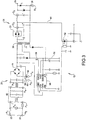
Fig. 3 is a detailed electronic circuit diagram of an exemplary switched mode power supply circuit; -
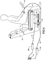
Fig. 4 is a cutaway side view of the chair ofFig. 1 , illustrating how static electric charges are generated and propagate through the power supply coupled to the chair and also to other devices in contact with the user, such as a laptop computer; -
Fig. 5 is another view of the simplified electronic circuit diagram ofFig. 2 , showing the discharge path of a static electric charge in a circuit without the benefit of the disclosed improvements; -
Fig. 6 is another view of the detailed electronic circuit diagram ofFig. 3 , showing the discharge path of a static electric charge in a circuit without the benefit of the disclosed improvements; -
Fig. 7 is a simplified block diagram of a power supply employing a first embodiment of the protective spark gap structure; -
Fig. 8 is a simplified block diagram of a power supply employing a first embodiment of the protective spark gap structure; -
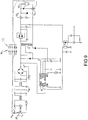
Fig. 9 is a detailed electronic circuit diagram of a power supply similar to that ofFig. 3 , but including the spark gap structure ofFig. 7 and illustrating several different possible attachment points to which the spark gap structure may be coupled; -
Fig. 10 is a partial plan view of a printed circuit board showing one embodiment of the spark gap structure employing discharge pins; -
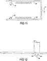
Fig. 11 is a partial plan view of a printed circuit board showing another embodiment of the spark gap structure employing spaced apart heat sinks; -
Fig. 12 is a detailed view of a power supply circuit component with leads configured in spaced relation to define a discharge gap. - Corresponding reference numerals indicate corresponding parts throughout the several views of the drawings.
- Example embodiments will now be described more fully with reference to the accompanying drawings.
- The electrostatic discharge protection technique will be described here in connection with two typical use cases: a motorized chair that uses a DC power supply to energize the motors and controller circuits, and a laptop computer that uses a DC power supply to charge the internal battery and to provide operating power to the laptop. These are exemplary devices as the circuits disclosed here may be applicable to other types of devices powered by a DC power supply that is ordinarily plugged into an AC outlet when in use.
- Referring to
Figure 1 , an exemplary power assistedrecliner chair 10.Chair 10 is also exemplary of an electrically operated lift chair, a primary difference between recliner chairs and lift chairs being the respective range of motor assisted motions. Power to operate the motors and other electrical and electronic components ofchair 10 is derived from aDC power supply 12 that is in turn coupled to a source of alternating (AC) current, such as anAC wall outlet 14.Chair 10 may be provided with acontroller 15, mounted on an arm of the chair. Thecontroller 15 is powered by the power supply and provides control voltages that power internal motors (not shown) that adjust the seat back and leg rest portions of the chair. As an alternative to, or in addition to the arm-mountedcontroller 15, adetachable controller 16 may be provided.Controller 16 functions essentially the same ascontroller 15, but is attached to the internal electronic components via an umbilical cord as illustrated. As a third alternative, the internal electronic components of the chair can include a radio circuit compatible with Bluetooth or WiFi protocols, to allow the char to be controlled remotely from a handheld portable device, such as a smartphone or tablet computer. -
Power supply 12 is preferably a switched mode power supply. Switched mode power supplies convert the standard 60 Hz. (or 50 Hz. in some locations) AC power into an alternating current of higher frequency. This is typically done with a solid state device such as a switching transistor. By converting the standard AC power to a higher frequency, much smaller step down transformers can be used, thus resulting in a much smaller and more convenient power supply package that is better suited for consumer applications. Once the voltage of this higher frequency alternating current has been stepped down to a voltage compatible with the DC motors and controller circuits, the lower voltage is rectified to convert it to the desired DC voltage. Thus the switched mode power supply has an AC portion, on the primary side of the step down transformer, and a DC portion, on the secondary side of the step down transformer. - By way of further explanation,
Figure 2 shows an exemplary switched mode power supply circuit in block diagram form. The power supply circuit includes anAC circuit portion 20 which is adapted for coupling to a source of alternating current as atAC input terminals 22.Terminals 22 are connected to a suitable power cord for connecting to an AC wall outlet. The power supply circuit also includes aDC circuit portion 24 having positive andnegative DC terminals 26, which are then connected to the device being powered by the power supply. The power supply depicted inFigure 2 is exemplary of a switching mode power supply that includes anactive switching component 28 that produces a switched alternating current at a frequency higher than the frequency of the source of alternating current supplied by the wall outlet. As illustrated, the DC circuit portion and AC circuit portion are coupled together through atransformer 30, which provides the line of demarcation between the AC circuit portion and the DC circuit portion. -
Transformer 30 is wound to act as a voltage step down transformer. Adiode 32 for other suitable rectifier device converts the stepped-down voltage at the secondary side oftransformer 30 into direct current which is then filtered byfilter capacitors 34. Azener diode 36, or other suitable voltage regulating device, clamps the output DC voltage at the desired nominal operating voltage for the intended application. - In the illustrated embodiment, the
active switching component 28 is driven by anelectronic driver circuit 38.Circuit 38 forms part of afeedback circuit 40 that supplies control pulses to theactive switching component 28 at the rate required to maintain the DC voltage output onterminals 26 at the desired voltage under different loads. The feedback circuit includes anoptical coupler 42 which electrically isolates the DC circuit portion form the AC circuit portion Thedriver circuit 38 is powered by a DC supply voltage obtained using abridge rectifier 44 andfilter capacitor 46. It should be noted that thebridge rectifier 44 andfilter capacitor 46 provide DC operating voltage to power theactive switching component 28 and thedriver circuit 38, although these components are on the AC circuit portion of the power supply. - An electromagnetic interference (EMI)
filter 48 is included across the line (L) and neutral (N) sides of the AC input terminals to protect the circuit from voltage surges and electrical noise entering the circuit through the AC power cord. - The
AC circuit portion 20 has an AC ground designated by theAC ground symbol 50, which appears at numerous points within theAC circuit portion 20. For example, one of the terminals of thebridge rectifier 44 is coupled to the AC ground as are a number of capacitors in the AC circuit potion. Likewise, theactive switching component 28 coupled toAC ground 50 through abias resistor 52; anddriver circuit 38 is likewise referenced to circuit ground at itsground pin 54. - The
DC circuit portion 24 has itsown DC ground 56. A different symbol has been used for the DC ground to differentiate it from the AC ground inFigure 2 . Note that in the illustrated embodiment, the negative one of theDC terminals 26 is coupled toDC ground 56. It is also possible to construct a circuit with the opposite polarity, where the positive DC terminal is coupled to ground. Either option is possible depending on the requirements of the power device. -
Figure 3 provides a more detailed circuit diagram of one embodiment of power supply. Where applicable, the same reference numerals as inFigure 2 have been used to designate like or comparable components. As discussed in connection withFigure 3 ,transformer 30 generally defines the line of demarcation between theAC circuit portion 20 andDC circuit portion 24. - By examining the circuit of
Figure 3 (and also the more generalized circuit ofFigure 2 ), it is seen that the AC and DC grounds are electrically isolated to substantially inhibit the flow of direct current there between. Becausetransformer 30 has separate primary and secondary windings, DC current on the secondary side of the transformer does not flow through to the primary side. Similarly, the DC voltage measured byfeedback resistor 41 does not result in current flowing through theoptical coupler 42, as this device is designed not to permit the flow of DC current through it. Careful inspection of the circuit ofFigure 3 shows that acapacitor 58 has been provided to couple between theAC ground 50 and theDC ground 56. Of course, this capacitor also blocks the flow of direct current between the AC ground and the DC ground. - When a static electricity charge enters the circuit of
Figure 3 at theDC terminals 26, significant damage to the power supply circuit can ensue as the charge races across the connected components in order to seek the lower potential of theAC input terminals 22. In this regard, because the AC input terminals are plugged into a power outlet, which is in turn coupled to the AC power grid, the static electric charge seeks to return to earth (to which the AC power grid is firmly rooted). Using the circuit ofFigure 2 as an example,Figure 5 shows the exemplary paths by which the static electric charge travels en route from theDC terminals 26 to theAC terminals 22. As can be seen, this discharge path traverses many, if not all, of the delegate electronic circuits comprising the power supply. Because the circuits are not designed to operate at the elevated voltages produced by static electricity, permanent damage can be caused. - There are many ways that static electricity find its way into the delicate electronic components of the
power supply 12. One very common way is that static electricity generated by persons as they walk across carpet or slide into and out of chairs and sofas. The effect is caused when two insulating objects, such as a person's clothing and the cloth covering a chair, are rubbed together. The effect is most prevalent at low humidity levels. -
Figure 4 shows how static electricity can be generated and find its way into delicate power supply circuits where significant damage can be done. As illustrated inFigure 4 , a person seated inchair 10, holdinglaptop computer 70, slides forward to exit the chair. In so doing, the person's posterior rubs against the fabric of thechair 11, which causes a separation of positive (+) and negative (-) charges as the cloth of the person's clothing rubs against the cloth or other material from which the chair is made. Because the person's clothing, the chair fabric or other material are relatively poor conductors of electricity, a negative charge is stored in one material and a positive charge in the other. As illustrated inFigure 4 , the person's clothing is shown as having a positive charge, while the fabric of the chair is shown as having a negative charge. So long as the person remains seated, these positive and negative charges will be attracted to one another and thus will tend to remain in the localized region where the respective insulative surfaces touch one another. However, when the person stands up, these two insulating surfaces become separated and the respective positive and negative charges are no longer attracted to one another. - Thus, the chair in
Figure 4 becomes negatively charged while the person (and objects held by the person) become positively charged. InFigure 4 , the person is holding alaptop computer 70 and thus the laptop computer will also become positively charged. - Because both the
chair 10 and thelaptop computer 70 are coupled to theirrespective power supplies AC power outlet 14. In this regard, it will be appreciated that theAC power outlet 14 is connected to the electric power grid maintained by the electric service utility company. This power grid is at many points carefully grounded to earth, thus the AC power outlet represents a very large earth sink to attract both positive and negative charges. Thus for example inFigure 4 , the negative (-) charges, initially deposited on the chair'scushion fabric 11, will flow through thecushion 13 andframe 17. From the frame, the charges then enter thecontrol circuitry 17 and motor(s) 19. Because thecontrol circuitry 17 is coupled to thepower supply 12a, the charge follows the DC power supply leads 21 and thus enters thepower supply 12 associated with the chair controller. - Similarly, as the person stands away from the chair, the positive (+) charges initially deposited on the person's clothing will flow into the
laptop computer 70 and then follow the DC power supply leads 23 and thereby enter thepower supply 12b of the laptop computer. - Whether the charges are positive or negative, they will flow through the power supply circuits generally as illustrated in
Figure 5 . Note that the electric charges enter the power supply circuit through theDC terminals 26 and then flow through many, if not all, of the delicate electronic components, ultimately exiting the power supply at theAC input terminals 22. In the case of the power supply associated with thechair 10, the static charge is a negative charge (based on the example ofFigure 4 ). In the case of thelaptop computer 70 being held by the person, the charge would be a positive charge (based on the example ofFigure 4 ). In either case, these static charges will quickly pass through the respective power supply circuits, causing damage to the delicate electronics area. By way of further explanation,Figure 6 shows the typical static electricity discharge path through the components of the power supply ofFigure 3 . - To solve the static electricity discharge problem, the improved power supply circuit employs a static electricity discharge structure that routes the static electricity energy in a path that avoids the delicate electronic components. To implement this structure the circuit defines a first attachment point that provides an energy pathway to the AC ground, and a second attachment point that provides an energy pathway to the DC ground. To these first and second attachment points a spark gap structure is coupled. The spark gap structure is configured to provide a static electricity energy path between the first and second attachment points. The spark gap structure is itself configured to substantially inhibit the flow of direct current between the first and second attachment points (i.e., the spark gap structure does not create a short circuit between the first and second attachment points).
Figures 7 and 8 diagrammatically illustrate this. Referring toFigure 7 , theAC circuit portion 20 has at least oneattachment point 72 that provides an energy pathway toAC ground 50. Similarly, theDC circuit portion 24 has at least oneattachment point 74 that provides anenergy pathway 75 toDC ground 56. Aspark gap structure 76 is coupled between the attachment points 72 and 74, as illustrated. InFigure 7 , the exemplary spark gap structure comprises one or a plurality of pairs of discharge pins 78 (three pairs are shown inFigure 6 ). These discharge pins define an air gap having a separation distance between 2mm and 8mm, and preferably between 3mm and 7mm, with one presently preferred embodiment having a distance of 6.2 mm. -
Figure 8 shows an alternate embodiment where thespark gap structure 76 comprises a pair ofconductive surfaces 80 that are spaced apart to define a separation distance of between 2mm and 8mm and preferably between 4mm and 7mm. These conductive surfaces may be implemented using metal components having other function within the circuit, such as a pair of spaced apart heat sinks, or a spaced apart set of wire leads on a circuit component such as a capacitor. Alternatively, the spark gap structure may be implemented using a gas discharge tube device. - In implementing the improved power supply circuit there can often be several different choices for implementing the first and second attachment points. Preferably the chosen are points are disposed on the respective AC circuit portions and DC circuit portions where active electronic components are not proximally attached. In
Figure 2 , for example, suitable AC portion attachment points are designated as A1-A5 and suitable DC portion attachment points are designated as D1-D2. Being coupled between the respective AC portion and DC portion attachment points, the spark gap structure essentially routes the static electric discharge around the delicate electronic components. Thus a spark gap structure coupled between attachment points D2 and A1, for example, will route the static electric discharge energy directly from point D2 to point A1, bypassing all of the delicate electronic components in between. Other connections between attachment points D1 and/or D2 and one or more of points A1-A5 will accomplish the same circuit protection. -
Figure 3 shows suitable attachment points for that circuit as well. These have been identified as points A1-A7 (on the AC circuit portion) and D1-D4 (on the DC circuit portion). Where applicable, like designations have been used to match those ofFigure 2 . Because the circuit ofFigure 3 is more detailed than that ofFigure 2 , more suitable attachment points have been shown. Of particular note are the attachment points A5 and D4. These correspond to the AC circuit portion side and DC circuit portion side ofcapacitor 58. Whilecapacitor 58 appears inFigure 3 to be within the AC circuit portion, it is actually serving to couple the AC ground with the DC ground. Thuscapacitor 58 can be said to define a line of demarcation between the AC circuit portion and the DC circuit portion. As shown inFigure 12 , capacitor can be mounted on a circuit board or other suitable connection points, so that its leads extend outwardly and then inwardly to define a spark gap structure. - Referring now to
Figure 9 , the circuit ofFigure 6 has been shown in modified form to include thespark gap structure 76 coupled between an AC circuit portion attachment point and a DC circuit portion attachment point. For illustration purposes, the attachment points A1 and D1 have been used. As can be seen, when electrostatic energy enters theDC terminals 26, the electrostatic energy is routed through thespark gap structure 76 , bypassing all of the delicate electronic components. Compare this withFigure 6 , where the spark gap structure is not used and the electrostatic energy traverses all or most of the delicate electronic components, causing damage. - While one
spark gap structure 76 comprising five pairs of discharge pins 78 has been illustrated inFigure 9 , it will be understood that the number of spark gap structures employed, and the number of individual pairs of discharge pins can be varied. For example, if desired a second spark gap structure might be coupled between attachment points A4 and D2, or between any other of the suitable AC circuit portion and DC circuit portion attachment points. -
Figures 2 and3 have illustrated some of the possible AC circuit portion and DC circuit portion attachment points, from the schematic diagram viewpoint. In an actual physical embodiment, the attachment points may be incorporated into regions or circuit traces of a printed circuit board to which the electronic components of the power supply are attached according to the schematic diagram.Figure 10 shows how aspark gap structure 76 comprising plural pairs of discharge pins 78 can be manufactured as part of the printed circuit board. The plural pairs of discharge pins are separated to define a gap of distance d. In one embodiment the distance d is in a range between 4 mm and 7 mm, although a distance d is in a range between 2 mm and 8 mm may also be used. For example, in the embodiment shown inFigure 10 , which has been enlarged for ease of viewing, the distance d is 6.4 mm. - In this case, the metallic circuit traces are disposed on one side of the printed
circuit board substrate 84. In this way, the metallic discharge pins are exposed to atmosphere so that static electricity can jump between the pairs of traces. In some circuit board manufacturing processes the circuit traces are coated with a protective, non-conductive coating. If such coating is provided, the regions around the metallic discharge pins should be masked when applying the coating, so that the discharge pins remain exposed to atmosphere to permit static discharge during use. While a single spark gap structure implemented as circuit board traces has been illustrated inFigure 10 , it should be understood that several such spark gap structures can be employed, and these can be coupled to the same attachment points or to different attachment points as may be dictated by physical or manufacturing constraints. - Another alternate physical implementation for the spark gap structure is shown in
Figure 11 . In this embodiment metal heat sinks are provided to dissipate heat from components on the respective AC and DC circuit portions. For example, on the AC circuit portion, the active switching component (e.g.,component 28 ofFigs 2 and3 ) may be thermally coupled toheat sink 90. On the DC circuit portion thediode 32 may be thermally coupled toheat sink 92. These two heat sinks are then positioned as shown inFigure 11 , so that they define an air gap spacing d, sized as discussed above, so that the two heat sinks may serve as a spark gap structure. These heat sinks are electrically coupled to a suitable attachment point, such as those discussed above. InFigure 11 ,heat sink 90 is electrically coupled to AC ground by being conductively attached to the AC side chassis to which all of the AC grounding points are attached. To prevent shorting of theactive switching component 28, that a mica insulator (not shown) is used betweencomponent 28 andheat sink 90. InFigure 11 ,heat sink 92 is conductively attached to attachment point D3, which is also electrically coupled to the cathode (negative terminal) of diode 32 (seeFigures 2 and3 ). - A third physical implementation for the spark gap structure is shown in
Figure 12 . In this embodiment the two leads 93 ofcapacitor 58 are extended outwardly and bent inwardly, as shown, to form a spark gap as at 94. A fourth physical implementation, not shown, employs a gas discharge device coupled between the attachment points of respective AC and DC circuit portions. - While different physical implementations for the spark gap structure have been discussed separately, these different implementations can be used in combination if desired.
- A method of configuring a protective circuit that inhibits the flow of ESD in a power supply that converts alternating current (AC) into direct current (DC) for powering device can also be carried out. Such a method can comprise the steps of:
- providing an AC circuit adapted for coupling to a source of alternating current wherein the AC circuit has a first common reference point that defines an AC reference point;
- providing a DC circuit coupled to the AC circuit wherein the DC circuit has direct current terminals for coupling to the powered device and has a second common reference point that defines a DC reference point;
- establishing electrical isolation between the AC and DC reference points to substantially inhibit the flow of direct current there between;
- providing a first attachment point that serves as an energy pathway to the AC reference point;
- providing a second attachment point that serves as an energy pathway to the DC reference point; and
- creating a spark gap structure coupled to the first and second attachment points that is configured to substantially inhibit the flow of direct current between the first and second attachment points while providing a static electricity energy path between the first and second attachment points.
- Alternatively, such a method can comprise the steps of:
- providing an AC circuit adapted for coupling to a source of alternating current wherein the AC circuit has a first common reference point that defines an AC reference point;
- providing a DC circuit coupled to the AC circuit wherein the DC circuit has direct current terminals for coupling to the powered device and has a second common reference point that defines a DC reference point;
- establishing electrical isolation between the AC and DC reference points to substantially inhibit the flow of direct current there between;
- providing a first attachment point defined on a printed circuit board that serves as an energy pathway to the AC reference point;
- providing a second attachment point defined on a printed circuit board that serves as an energy pathway to the DC reference point; and
- creating at least one pair of spaced apart circuit traces, one trace of the pair being electrically connected to the first attachment point and the other trace of the pair being electrically connected to the second attachment point to serve as a spark gap structure coupled between the first and second attachment points and configured to substantially inhibit the flow of direct current between the first and second attachment points while providing a static electricity energy path between the first and second attachment points.
Claims (15)
- A power supply (12) for converting alternating current AC, into direct current, DC, for powering a device, the power supply (12) comprising:an AC circuit (20) adapted for coupling to a source of alternating current and having a first common reference point that defines an AC reference point;a DC circuit (24) coupled to the AC circuit (20) and providing direct current terminals (26) for coupling to the powered device and having a second common reference point that defines a DC reference point;the AC and DC reference points being electrically isolated to substantially inhibit the flow of direct current there between;a first attachment point that provides an energy pathway to the AC reference point;a second attachment point that provides an energy pathway to the DC reference point;a spark gap structure (76) coupled to the first and second attachment points, the spark gap structure (76) being configured to substantially inhibit the flow of direct current between the first and second attachment points while providing a static electricity energy path between the first and second attachment points,characterized in that:the DC circuit (24) includes a first metal heat sink structure (92) and the AC circuit includes a second metal heat sink structure (90), whereinthe first metal heat sink structure (92) defines a first portion of the spark gap structure (76), the second metal heat sink structure (90) defines a second portion of the spark gap structure (76), and the first metal heat sink structure (92) dissipates heat from a component of the DC circuit portion other than the spark gap structure (76) itself.
- The power supply of claim 1 wherein the AC circuit (20) includes a second metal heat sink structure (90) attached to a component of the AC circuit and wherein said metal heat sink structure (90) defines a portion of the spark gap structure (76).
- The power supply (12) of claim 2 wherein the first and second metal heat sink structures are spaced apart a separation distance (d) of between 2 mm and 8 mm.
- The power supply (12) of claim 2 wherein the first and second heat sink structures are spaced apart a separation distance (d) of between 4 mm and 7 mm.
- The power supply (12) of claim 1 wherein the AC circuit (24) includes a second metal heat sink structure (90) attached to a component of the AC circuit and wherein said second metal heat sink structure (90) defines a second portion of the spark gap structure (76), the first and second metal heat sink structures being positioned in spaced relation to inhibit the flow of direct current between the first and second heat sink structures while providing a static electricity energy path there between.
- The power supply (12) of claim 1 wherein the AC circuit (20) and the DC circuit (24) function as a switched mode power supply.
- The power supply (12) of claim 1 wherein the AC circuit (20) includes at least one active switching component (28) that produces a switched alternating current at a frequency higher than the frequency of the source of alternating current, wherein the DC circuit (24) is coupled to the AC circuit (20) through a transformer (30) and wherein the DC circuit (24) includes a rectifier that converts the switched alternating current into direct current.
- The power supply (12) of claim 1 wherein the AC circuit (20) and the DC circuit (24) are coupled by a transformer (30) that defines a line of demarcation between the AC circuit (20) and the DC circuit (24).
- The power supply (12) of claim 1 wherein the AC reference point is selected from the group consisting of AC ground, AC live and AC neutral.
- The power supply (12) of claim 1 wherein the DC reference point is selected from the group consisting of a DC positive terminal and a DC negative terminal.
- A method of inhibiting the flow of electrostatic discharge in a power supply (12) that converts alternating current, AC, into direct current, DC, for powering a device, the method comprising:providing an AC circuit (20) adapted for coupling to a source of alternating current wherein the AC circuit (20) has a first common reference point that defines an AC reference point, and the AC circuit (20) includes a second metal heat sink structure (90);providing a DC circuit (24) coupled to the AC circuit (20) wherein the DC circuit (24) has direct current terminals (26) for coupling to the powered device and has a second common reference point that defines a DC reference point, and the DC circuit (24) includes a first metal heat sink structure (92);establishing electrical isolation between the AC and DC reference points to substantially inhibit the flow of direct current there between;providing a first attachment point that serves as an energy pathway to the AC reference point;providing a second attachment point that serves as an energy pathway to the DC reference point; andcreating a spark gap structure (76) coupled to the first and second attachment points that is configured to substantially inhibit the flow of direct current between the first and second attachment points while providing a static electricity energy path between the first and second attachment points,characterized in that:the first metal heat sink structure (92) forms a first portion of the spark gap structure (76) and dissipates heat from a component of the DC circuit portion other than the spark gap structure (76) itself,the second metal heat sink structure (90) forms a second portion of the spark gap structure (76), andthe first and second metal heat sink structures are positioned in spaced relation to inhibit the flow of direct current between the first and second metal heat sink structures while providing a static electricity path there between.
- The method of claim 11 wherein the first and second metal heat sink structures are spaced apart a separation distance (d) of between 2 mm and 8 mm.
- The method of claim 11 wherein the first and second metal heat sink structures are spaced apart a separation distance (d) of between 4 mm and 7 mm.
- The method of claim 11 wherein the AC circuit (20) includes at least one active switching component (28) that produces a switched alternating current at a frequency higher than the frequency of the source of alternating current, wherein the DC circuit (24) is coupled to the AC circuit (20) through a transformer (30) and wherein the DC circuit (24) includes a rectifier that converts the switched alternating current into direct current.
- The method of claim 11 wherein the AC circuit (20) and the DC circuit (24) are coupled by a transformer (30) that defines a line of demarcation between the AC circuit (20) and the DC circuit (24).
Applications Claiming Priority (2)
| Application Number | Priority Date | Filing Date | Title |
|---|---|---|---|
| US14/631,311 US9281683B1 (en) | 2015-02-25 | 2015-02-25 | Electrostatic discharge protection and method in power supply |
| PCT/US2015/017761 WO2016137469A1 (en) | 2015-02-25 | 2015-02-26 | Electrostatic discharge protection and method in power supply |
Publications (3)
| Publication Number | Publication Date |
|---|---|
| EP3262742A1 EP3262742A1 (en) | 2018-01-03 |
| EP3262742A4 EP3262742A4 (en) | 2018-08-29 |
| EP3262742B1 true EP3262742B1 (en) | 2019-12-25 |
Family
ID=55410539
Family Applications (1)
| Application Number | Title | Priority Date | Filing Date |
|---|---|---|---|
| EP15883563.7A Active EP3262742B1 (en) | 2015-02-25 | 2015-02-26 | Electrostatic discharge protection and method in power supply |
Country Status (15)
| Country | Link |
|---|---|
| US (1) | US9281683B1 (en) |
| EP (1) | EP3262742B1 (en) |
| JP (1) | JP6402258B2 (en) |
| KR (1) | KR20170118908A (en) |
| CN (1) | CN107534385B (en) |
| AU (2) | AU2015384155A1 (en) |
| BR (1) | BR112017018332A2 (en) |
| CA (1) | CA2977024C (en) |
| IL (1) | IL254002B (en) |
| MX (1) | MX365676B (en) |
| MY (1) | MY164589A (en) |
| NZ (1) | NZ734643A (en) |
| PH (1) | PH12017501496A1 (en) |
| WO (1) | WO2016137469A1 (en) |
| ZA (1) | ZA201705875B (en) |
Families Citing this family (3)
| Publication number | Priority date | Publication date | Assignee | Title |
|---|---|---|---|---|
| JP2017530681A (en) * | 2014-09-25 | 2017-10-12 | アルパイン メディア | Method and device for providing energy to a system in a mobile body |
| JP7175015B2 (en) * | 2020-01-10 | 2022-11-18 | クロイ電機株式会社 | power supply |
| TWI859054B (en) * | 2024-01-05 | 2024-10-11 | 旺宏電子股份有限公司 | Power conversion device and electrostatic discharge circuit |
Citations (1)
| Publication number | Priority date | Publication date | Assignee | Title |
|---|---|---|---|---|
| EP2779793A2 (en) * | 2013-03-06 | 2014-09-17 | E.R.C. Highlight S.r.l. | Lighting apparatus with device for protection against electrostatic discharges for led modules |
Family Cites Families (20)
| Publication number | Priority date | Publication date | Assignee | Title |
|---|---|---|---|---|
| US4586105A (en) * | 1985-08-02 | 1986-04-29 | General Motors Corporation | High voltage protection device with a tape covered spark gap |
| KR930011479B1 (en) * | 1991-12-31 | 1993-12-08 | 주식회사 금성사 | Back-up circuit |
| US5555150A (en) * | 1995-04-19 | 1996-09-10 | Lutron Electronics Co., Inc. | Surge suppression system |
| US5892669A (en) * | 1996-11-29 | 1999-04-06 | Samsung Electronics Co., Ltd. | Electronic products with improved surge protecting circuit |
| US5995353A (en) * | 1997-06-17 | 1999-11-30 | Hewlett-Packard Company | Apparatus for discharging an electrostatic discharge via a spark gap coupled in series with a high impedance network |
| JPH11206160A (en) * | 1998-01-13 | 1999-07-30 | Hiroyuki Matsuda | Power booster |
| GB2334626B (en) * | 1998-02-20 | 2003-01-29 | Mitel Corp | Spark gap for hermetically packaged integrated circuits |
| US6002569A (en) * | 1998-06-29 | 1999-12-14 | Hewlett-Packard Company | Electrostatic discharge protection apparatus |
| JP2003143752A (en) * | 2001-10-30 | 2003-05-16 | Sony Corp | AC adapter |
| US6781326B2 (en) * | 2001-12-17 | 2004-08-24 | Q Technology Incorporated | Ballast with lamp sensor and method therefor |
| US7312970B2 (en) * | 2004-01-09 | 2007-12-25 | Emerson Electric Co. | Low cost surge protection |
| ATE371971T1 (en) * | 2004-06-30 | 2007-09-15 | Research In Motion Ltd | SPARK GAP DEVICE AND METHOD FOR ELECTROSTATIC DISCHARGE PROTECTION |
| US8134817B2 (en) | 2008-08-12 | 2012-03-13 | Power Integrations, Inc. | Electrostatic discharge conducting pathway having a noise filter spark gap |
| US7948726B2 (en) | 2008-09-25 | 2011-05-24 | Panasonic Automotive Systems Company Of America, Division Of Panasonic Corporation Of North America | Electrostatic discharge (ESD) protection circuit and method |
| EP2329573A4 (en) * | 2008-09-25 | 2013-03-20 | Panasonic Automotive Sys Co Am | Electrostatic discharge (esd) protection circuit and method |
| JP2011206160A (en) | 2010-03-29 | 2011-10-20 | Fujifilm Corp | Radiographic system and method |
| JP2012043860A (en) | 2010-08-16 | 2012-03-01 | Panasonic Corp | Light-emitting device, backlight unit, liquid crystal display device, and lighting device |
| US8345400B2 (en) * | 2010-08-17 | 2013-01-01 | Lutron Electronics Co., Inc. | Surge suppression circuit for a load control device |
| US8787039B2 (en) * | 2012-07-18 | 2014-07-22 | Dialog Semiconductor Inc. | Hybrid adaptive power factor correction schemes for switching power converters |
| JP2014064392A (en) * | 2012-09-21 | 2014-04-10 | Sanken Electric Co Ltd | Switching power supply device |
-
2015
- 2015-02-25 US US14/631,311 patent/US9281683B1/en active Active
- 2015-02-26 MX MX2017010750A patent/MX365676B/en active IP Right Grant
- 2015-02-26 WO PCT/US2015/017761 patent/WO2016137469A1/en not_active Ceased
- 2015-02-26 MY MYPI2017703002A patent/MY164589A/en unknown
- 2015-02-26 KR KR1020177026835A patent/KR20170118908A/en not_active Abandoned
- 2015-02-26 CA CA2977024A patent/CA2977024C/en active Active
- 2015-02-26 NZ NZ734643A patent/NZ734643A/en unknown
- 2015-02-26 CN CN201580079110.4A patent/CN107534385B/en active Active
- 2015-02-26 BR BR112017018332-3A patent/BR112017018332A2/en not_active Application Discontinuation
- 2015-02-26 JP JP2017545260A patent/JP6402258B2/en not_active Expired - Fee Related
- 2015-02-26 AU AU2015384155A patent/AU2015384155A1/en not_active Abandoned
- 2015-02-26 EP EP15883563.7A patent/EP3262742B1/en active Active
-
2017
- 2017-08-15 IL IL254002A patent/IL254002B/en not_active IP Right Cessation
- 2017-08-17 PH PH12017501496A patent/PH12017501496A1/en unknown
- 2017-08-29 ZA ZA2017/05875A patent/ZA201705875B/en unknown
-
2019
- 2019-05-10 AU AU2019203309A patent/AU2019203309B2/en active Active
Patent Citations (1)
| Publication number | Priority date | Publication date | Assignee | Title |
|---|---|---|---|---|
| EP2779793A2 (en) * | 2013-03-06 | 2014-09-17 | E.R.C. Highlight S.r.l. | Lighting apparatus with device for protection against electrostatic discharges for led modules |
Also Published As
| Publication number | Publication date |
|---|---|
| IL254002B (en) | 2018-04-30 |
| WO2016137469A1 (en) | 2016-09-01 |
| ZA201705875B (en) | 2019-12-18 |
| NZ734643A (en) | 2019-05-31 |
| EP3262742A4 (en) | 2018-08-29 |
| KR20170118908A (en) | 2017-10-25 |
| MX2017010750A (en) | 2018-06-15 |
| CA2977024C (en) | 2019-09-10 |
| AU2019203309A1 (en) | 2019-05-30 |
| AU2015384155A1 (en) | 2017-08-31 |
| HK1244961A1 (en) | 2018-08-17 |
| CN107534385B (en) | 2019-11-29 |
| MY164589A (en) | 2018-01-12 |
| CA2977024A1 (en) | 2016-09-01 |
| EP3262742A1 (en) | 2018-01-03 |
| JP2018511908A (en) | 2018-04-26 |
| CN107534385A (en) | 2018-01-02 |
| AU2019203309B2 (en) | 2021-01-28 |
| JP6402258B2 (en) | 2018-10-10 |
| BR112017018332A2 (en) | 2018-04-17 |
| PH12017501496B1 (en) | 2018-01-15 |
| MX365676B (en) | 2019-06-10 |
| PH12017501496A1 (en) | 2018-01-15 |
| IL254002A0 (en) | 2017-10-31 |
| US9281683B1 (en) | 2016-03-08 |
| NZ753699A (en) | 2020-11-27 |
Similar Documents
| Publication | Publication Date | Title |
|---|---|---|
| AU2019203309B2 (en) | Electrostatic Discharge Protection And Method In Power Supply | |
| CN112787306B (en) | Grounding fault interruption and USB power supply electrical wiring equipment | |
| US8638536B2 (en) | Electrostatic discharge conducting pathway having a noise filter spark gap | |
| EP2840693B1 (en) | Three-phase power supply and system of LEDs with three-phase power supply | |
| US8913355B2 (en) | Totally insulated switched mode power supply | |
| KR20150026289A (en) | Power factor correction circuit | |
| CN102668292B (en) | Systems and methods for providing surge protection | |
| NZ753699B2 (en) | Electrostatic discharge protection and method in power supply | |
| JP5409316B2 (en) | Surge suppression circuit and lighting device | |
| HK1244961B (en) | Electrostatic discharge protection and method in power supply | |
| KR100455445B1 (en) | The automatic ground-earthing regulator in electric heat mat | |
| JPH05103421A (en) | Parallel operation connecting unit for ac power supply unit | |
| CN117441410A (en) | ESD protection of chip scale packaged LEDs | |
| KR100360318B1 (en) | Assortment adjuster of automatic earthing for electric mat | |
| TW201830840A (en) | Power supply unit | |
| JP2010226925A (en) | Protection circuit | |
| RU2319269C1 (en) | Device for protecting cutout in electric circuit with grounded neutral | |
| WO2020163367A1 (en) | Power supply for electric utility underground equipment | |
| JP4361923B2 (en) | GPT addition type ground voltage suppression device | |
| KR200258556Y1 (en) | The automatic ground-sorting regulator to form a imaginary ground point at a electric heat mat | |
| JP4133920B2 (en) | Negative potential treatment device | |
| TW202531682A (en) | Power generation equipment and electrical machinery | |
| JPS62275405A (en) | Apparatus for preventing electric shock of electric machinery |
Legal Events
| Date | Code | Title | Description |
|---|---|---|---|
| STAA | Information on the status of an ep patent application or granted ep patent |
Free format text: STATUS: THE INTERNATIONAL PUBLICATION HAS BEEN MADE |
|
| PUAI | Public reference made under article 153(3) epc to a published international application that has entered the european phase |
Free format text: ORIGINAL CODE: 0009012 |
|
| STAA | Information on the status of an ep patent application or granted ep patent |
Free format text: STATUS: REQUEST FOR EXAMINATION WAS MADE |
|
| 17P | Request for examination filed |
Effective date: 20170922 |
|
| AK | Designated contracting states |
Kind code of ref document: A1 Designated state(s): AL AT BE BG CH CY CZ DE DK EE ES FI FR GB GR HR HU IE IS IT LI LT LU LV MC MK MT NL NO PL PT RO RS SE SI SK SM TR |
|
| AX | Request for extension of the european patent |
Extension state: BA ME |
|
| DAX | Request for extension of the european patent (deleted) | ||
| A4 | Supplementary search report drawn up and despatched |
Effective date: 20180731 |
|
| RIC1 | Information provided on ipc code assigned before grant |
Ipc: H02M 3/335 20060101AFI20180725BHEP Ipc: H02H 9/04 20060101ALI20180725BHEP Ipc: H01L 23/62 20060101ALN20180725BHEP |
|
| STAA | Information on the status of an ep patent application or granted ep patent |
Free format text: STATUS: EXAMINATION IS IN PROGRESS |
|
| 17Q | First examination report despatched |
Effective date: 20181022 |
|
| REG | Reference to a national code |
Ref country code: DE Ref legal event code: R079 Ref document number: 602015044462 Country of ref document: DE Free format text: PREVIOUS MAIN CLASS: H02M0001320000 Ipc: H02M0003335000 |
|
| GRAP | Despatch of communication of intention to grant a patent |
Free format text: ORIGINAL CODE: EPIDOSNIGR1 |
|
| STAA | Information on the status of an ep patent application or granted ep patent |
Free format text: STATUS: GRANT OF PATENT IS INTENDED |
|
| RIC1 | Information provided on ipc code assigned before grant |
Ipc: H02M 3/335 20060101AFI20190620BHEP Ipc: H02H 9/04 20060101ALI20190620BHEP |
|
| INTG | Intention to grant announced |
Effective date: 20190717 |
|
| GRAS | Grant fee paid |
Free format text: ORIGINAL CODE: EPIDOSNIGR3 |
|
| GRAA | (expected) grant |
Free format text: ORIGINAL CODE: 0009210 |
|
| STAA | Information on the status of an ep patent application or granted ep patent |
Free format text: STATUS: THE PATENT HAS BEEN GRANTED |
|
| AK | Designated contracting states |
Kind code of ref document: B1 Designated state(s): AL AT BE BG CH CY CZ DE DK EE ES FI FR GB GR HR HU IE IS IT LI LT LU LV MC MK MT NL NO PL PT RO RS SE SI SK SM TR |
|
| REG | Reference to a national code |
Ref country code: GB Ref legal event code: FG4D |
|
| REG | Reference to a national code |
Ref country code: CH Ref legal event code: EP |
|
| REG | Reference to a national code |
Ref country code: AT Ref legal event code: REF Ref document number: 1218245 Country of ref document: AT Kind code of ref document: T Effective date: 20200115 |
|
| REG | Reference to a national code |
Ref country code: DE Ref legal event code: R096 Ref document number: 602015044462 Country of ref document: DE |
|
| REG | Reference to a national code |
Ref country code: IE Ref legal event code: FG4D |
|
| REG | Reference to a national code |
Ref country code: NL Ref legal event code: MP Effective date: 20191225 |
|
| PG25 | Lapsed in a contracting state [announced via postgrant information from national office to epo] |
Ref country code: BG Free format text: LAPSE BECAUSE OF FAILURE TO SUBMIT A TRANSLATION OF THE DESCRIPTION OR TO PAY THE FEE WITHIN THE PRESCRIBED TIME-LIMIT Effective date: 20200325 Ref country code: LT Free format text: LAPSE BECAUSE OF FAILURE TO SUBMIT A TRANSLATION OF THE DESCRIPTION OR TO PAY THE FEE WITHIN THE PRESCRIBED TIME-LIMIT Effective date: 20191225 Ref country code: FI Free format text: LAPSE BECAUSE OF FAILURE TO SUBMIT A TRANSLATION OF THE DESCRIPTION OR TO PAY THE FEE WITHIN THE PRESCRIBED TIME-LIMIT Effective date: 20191225 Ref country code: GR Free format text: LAPSE BECAUSE OF FAILURE TO SUBMIT A TRANSLATION OF THE DESCRIPTION OR TO PAY THE FEE WITHIN THE PRESCRIBED TIME-LIMIT Effective date: 20200326 Ref country code: NO Free format text: LAPSE BECAUSE OF FAILURE TO SUBMIT A TRANSLATION OF THE DESCRIPTION OR TO PAY THE FEE WITHIN THE PRESCRIBED TIME-LIMIT Effective date: 20200325 Ref country code: SE Free format text: LAPSE BECAUSE OF FAILURE TO SUBMIT A TRANSLATION OF THE DESCRIPTION OR TO PAY THE FEE WITHIN THE PRESCRIBED TIME-LIMIT Effective date: 20191225 Ref country code: LV Free format text: LAPSE BECAUSE OF FAILURE TO SUBMIT A TRANSLATION OF THE DESCRIPTION OR TO PAY THE FEE WITHIN THE PRESCRIBED TIME-LIMIT Effective date: 20191225 |
|
| REG | Reference to a national code |
Ref country code: LT Ref legal event code: MG4D |
|
| PG25 | Lapsed in a contracting state [announced via postgrant information from national office to epo] |
Ref country code: RS Free format text: LAPSE BECAUSE OF FAILURE TO SUBMIT A TRANSLATION OF THE DESCRIPTION OR TO PAY THE FEE WITHIN THE PRESCRIBED TIME-LIMIT Effective date: 20191225 Ref country code: HR Free format text: LAPSE BECAUSE OF FAILURE TO SUBMIT A TRANSLATION OF THE DESCRIPTION OR TO PAY THE FEE WITHIN THE PRESCRIBED TIME-LIMIT Effective date: 20191225 |
|
| PG25 | Lapsed in a contracting state [announced via postgrant information from national office to epo] |
Ref country code: AL Free format text: LAPSE BECAUSE OF FAILURE TO SUBMIT A TRANSLATION OF THE DESCRIPTION OR TO PAY THE FEE WITHIN THE PRESCRIBED TIME-LIMIT Effective date: 20191225 |
|
| PG25 | Lapsed in a contracting state [announced via postgrant information from national office to epo] |
Ref country code: EE Free format text: LAPSE BECAUSE OF FAILURE TO SUBMIT A TRANSLATION OF THE DESCRIPTION OR TO PAY THE FEE WITHIN THE PRESCRIBED TIME-LIMIT Effective date: 20191225 Ref country code: NL Free format text: LAPSE BECAUSE OF FAILURE TO SUBMIT A TRANSLATION OF THE DESCRIPTION OR TO PAY THE FEE WITHIN THE PRESCRIBED TIME-LIMIT Effective date: 20191225 Ref country code: PT Free format text: LAPSE BECAUSE OF FAILURE TO SUBMIT A TRANSLATION OF THE DESCRIPTION OR TO PAY THE FEE WITHIN THE PRESCRIBED TIME-LIMIT Effective date: 20200520 Ref country code: CZ Free format text: LAPSE BECAUSE OF FAILURE TO SUBMIT A TRANSLATION OF THE DESCRIPTION OR TO PAY THE FEE WITHIN THE PRESCRIBED TIME-LIMIT Effective date: 20191225 Ref country code: RO Free format text: LAPSE BECAUSE OF FAILURE TO SUBMIT A TRANSLATION OF THE DESCRIPTION OR TO PAY THE FEE WITHIN THE PRESCRIBED TIME-LIMIT Effective date: 20191225 |
|
| PG25 | Lapsed in a contracting state [announced via postgrant information from national office to epo] |
Ref country code: IS Free format text: LAPSE BECAUSE OF FAILURE TO SUBMIT A TRANSLATION OF THE DESCRIPTION OR TO PAY THE FEE WITHIN THE PRESCRIBED TIME-LIMIT Effective date: 20200425 Ref country code: SK Free format text: LAPSE BECAUSE OF FAILURE TO SUBMIT A TRANSLATION OF THE DESCRIPTION OR TO PAY THE FEE WITHIN THE PRESCRIBED TIME-LIMIT Effective date: 20191225 Ref country code: SM Free format text: LAPSE BECAUSE OF FAILURE TO SUBMIT A TRANSLATION OF THE DESCRIPTION OR TO PAY THE FEE WITHIN THE PRESCRIBED TIME-LIMIT Effective date: 20191225 |
|
| REG | Reference to a national code |
Ref country code: DE Ref legal event code: R119 Ref document number: 602015044462 Country of ref document: DE |
|
| REG | Reference to a national code |
Ref country code: CH Ref legal event code: PL |
|
| REG | Reference to a national code |
Ref country code: BE Ref legal event code: MM Effective date: 20200229 |
|
| PG25 | Lapsed in a contracting state [announced via postgrant information from national office to epo] |
Ref country code: ES Free format text: LAPSE BECAUSE OF FAILURE TO SUBMIT A TRANSLATION OF THE DESCRIPTION OR TO PAY THE FEE WITHIN THE PRESCRIBED TIME-LIMIT Effective date: 20191225 Ref country code: DK Free format text: LAPSE BECAUSE OF FAILURE TO SUBMIT A TRANSLATION OF THE DESCRIPTION OR TO PAY THE FEE WITHIN THE PRESCRIBED TIME-LIMIT Effective date: 20191225 Ref country code: LU Free format text: LAPSE BECAUSE OF NON-PAYMENT OF DUE FEES Effective date: 20200226 Ref country code: MC Free format text: LAPSE BECAUSE OF FAILURE TO SUBMIT A TRANSLATION OF THE DESCRIPTION OR TO PAY THE FEE WITHIN THE PRESCRIBED TIME-LIMIT Effective date: 20191225 |
|
| PLBE | No opposition filed within time limit |
Free format text: ORIGINAL CODE: 0009261 |
|
| STAA | Information on the status of an ep patent application or granted ep patent |
Free format text: STATUS: NO OPPOSITION FILED WITHIN TIME LIMIT |
|
| REG | Reference to a national code |
Ref country code: AT Ref legal event code: MK05 Ref document number: 1218245 Country of ref document: AT Kind code of ref document: T Effective date: 20191225 |
|
| PG25 | Lapsed in a contracting state [announced via postgrant information from national office to epo] |
Ref country code: CH Free format text: LAPSE BECAUSE OF NON-PAYMENT OF DUE FEES Effective date: 20200229 Ref country code: SI Free format text: LAPSE BECAUSE OF FAILURE TO SUBMIT A TRANSLATION OF THE DESCRIPTION OR TO PAY THE FEE WITHIN THE PRESCRIBED TIME-LIMIT Effective date: 20191225 Ref country code: LI Free format text: LAPSE BECAUSE OF NON-PAYMENT OF DUE FEES Effective date: 20200229 |
|
| 26N | No opposition filed |
Effective date: 20200928 |
|
| PG25 | Lapsed in a contracting state [announced via postgrant information from national office to epo] |
Ref country code: AT Free format text: LAPSE BECAUSE OF FAILURE TO SUBMIT A TRANSLATION OF THE DESCRIPTION OR TO PAY THE FEE WITHIN THE PRESCRIBED TIME-LIMIT Effective date: 20191225 Ref country code: IT Free format text: LAPSE BECAUSE OF FAILURE TO SUBMIT A TRANSLATION OF THE DESCRIPTION OR TO PAY THE FEE WITHIN THE PRESCRIBED TIME-LIMIT Effective date: 20191225 Ref country code: IE Free format text: LAPSE BECAUSE OF NON-PAYMENT OF DUE FEES Effective date: 20200226 Ref country code: DE Free format text: LAPSE BECAUSE OF NON-PAYMENT OF DUE FEES Effective date: 20200901 Ref country code: FR Free format text: LAPSE BECAUSE OF NON-PAYMENT OF DUE FEES Effective date: 20200229 |
|
| PG25 | Lapsed in a contracting state [announced via postgrant information from national office to epo] |
Ref country code: BE Free format text: LAPSE BECAUSE OF NON-PAYMENT OF DUE FEES Effective date: 20200229 Ref country code: PL Free format text: LAPSE BECAUSE OF FAILURE TO SUBMIT A TRANSLATION OF THE DESCRIPTION OR TO PAY THE FEE WITHIN THE PRESCRIBED TIME-LIMIT Effective date: 20191225 |
|
| PG25 | Lapsed in a contracting state [announced via postgrant information from national office to epo] |
Ref country code: TR Free format text: LAPSE BECAUSE OF FAILURE TO SUBMIT A TRANSLATION OF THE DESCRIPTION OR TO PAY THE FEE WITHIN THE PRESCRIBED TIME-LIMIT Effective date: 20191225 Ref country code: MT Free format text: LAPSE BECAUSE OF FAILURE TO SUBMIT A TRANSLATION OF THE DESCRIPTION OR TO PAY THE FEE WITHIN THE PRESCRIBED TIME-LIMIT Effective date: 20191225 Ref country code: CY Free format text: LAPSE BECAUSE OF FAILURE TO SUBMIT A TRANSLATION OF THE DESCRIPTION OR TO PAY THE FEE WITHIN THE PRESCRIBED TIME-LIMIT Effective date: 20191225 |
|
| PG25 | Lapsed in a contracting state [announced via postgrant information from national office to epo] |
Ref country code: MK Free format text: LAPSE BECAUSE OF FAILURE TO SUBMIT A TRANSLATION OF THE DESCRIPTION OR TO PAY THE FEE WITHIN THE PRESCRIBED TIME-LIMIT Effective date: 20191225 |
|
| PGFP | Annual fee paid to national office [announced via postgrant information from national office to epo] |
Ref country code: GB Payment date: 20260227 Year of fee payment: 12 |