EP3261173A1 - Communication device and antenna assembly thereof - Google Patents
Communication device and antenna assembly thereof Download PDFInfo
- Publication number
- EP3261173A1 EP3261173A1 EP16204573.6A EP16204573A EP3261173A1 EP 3261173 A1 EP3261173 A1 EP 3261173A1 EP 16204573 A EP16204573 A EP 16204573A EP 3261173 A1 EP3261173 A1 EP 3261173A1
- Authority
- EP
- European Patent Office
- Prior art keywords
- antenna
- main body
- housing
- mother board
- communication device
- Prior art date
- Legal status (The legal status is an assumption and is not a legal conclusion. Google has not performed a legal analysis and makes no representation as to the accuracy of the status listed.)
- Granted
Links
Images



Classifications
-
- H—ELECTRICITY
- H01—ELECTRIC ELEMENTS
- H01Q—ANTENNAS, i.e. RADIO AERIALS
- H01Q1/00—Details of, or arrangements associated with, antennas
- H01Q1/12—Supports; Mounting means
- H01Q1/22—Supports; Mounting means by structural association with other equipment or articles
- H01Q1/24—Supports; Mounting means by structural association with other equipment or articles with receiving set
- H01Q1/241—Supports; Mounting means by structural association with other equipment or articles with receiving set used in mobile communications, e.g. GSM
- H01Q1/242—Supports; Mounting means by structural association with other equipment or articles with receiving set used in mobile communications, e.g. GSM specially adapted for hand-held use
- H01Q1/243—Supports; Mounting means by structural association with other equipment or articles with receiving set used in mobile communications, e.g. GSM specially adapted for hand-held use with built-in antennas
-
- G—PHYSICS
- G06—COMPUTING OR CALCULATING; COUNTING
- G06F—ELECTRIC DIGITAL DATA PROCESSING
- G06F1/00—Details not covered by groups G06F3/00 - G06F13/00 and G06F21/00
- G06F1/16—Constructional details or arrangements
- G06F1/1613—Constructional details or arrangements for portable computers
- G06F1/1626—Constructional details or arrangements for portable computers with a single-body enclosure integrating a flat display, e.g. Personal Digital Assistants [PDAs]
-
- G—PHYSICS
- G06—COMPUTING OR CALCULATING; COUNTING
- G06F—ELECTRIC DIGITAL DATA PROCESSING
- G06F1/00—Details not covered by groups G06F3/00 - G06F13/00 and G06F21/00
- G06F1/16—Constructional details or arrangements
- G06F1/1613—Constructional details or arrangements for portable computers
- G06F1/1633—Constructional details or arrangements of portable computers not specific to the type of enclosures covered by groups G06F1/1615 - G06F1/1626
- G06F1/1656—Details related to functional adaptations of the enclosure, e.g. to provide protection against EMI, shock, water, or to host detachable peripherals like a mouse or removable expansions units like PCMCIA cards, or to provide access to internal components for maintenance or to removable storage supports like CDs or DVDs, or to mechanically mount accessories
- G06F1/1658—Details related to functional adaptations of the enclosure, e.g. to provide protection against EMI, shock, water, or to host detachable peripherals like a mouse or removable expansions units like PCMCIA cards, or to provide access to internal components for maintenance or to removable storage supports like CDs or DVDs, or to mechanically mount accessories related to the mounting of internal components, e.g. disc drive or any other functional module
-
- H—ELECTRICITY
- H01—ELECTRIC ELEMENTS
- H01Q—ANTENNAS, i.e. RADIO AERIALS
- H01Q1/00—Details of, or arrangements associated with, antennas
- H01Q1/36—Structural form of radiating elements, e.g. cone, spiral, umbrella; Particular materials used therewith
- H01Q1/38—Structural form of radiating elements, e.g. cone, spiral, umbrella; Particular materials used therewith formed by a conductive layer on an insulating support
-
- H—ELECTRICITY
- H01—ELECTRIC ELEMENTS
- H01Q—ANTENNAS, i.e. RADIO AERIALS
- H01Q1/00—Details of, or arrangements associated with, antennas
- H01Q1/48—Earthing means; Earth screens; Counterpoises
-
- H—ELECTRICITY
- H01—ELECTRIC ELEMENTS
- H01Q—ANTENNAS, i.e. RADIO AERIALS
- H01Q1/00—Details of, or arrangements associated with, antennas
- H01Q1/50—Structural association of antennas with earthing switches, lead-in devices or lightning protectors
-
- G—PHYSICS
- G06—COMPUTING OR CALCULATING; COUNTING
- G06F—ELECTRIC DIGITAL DATA PROCESSING
- G06F1/00—Details not covered by groups G06F3/00 - G06F13/00 and G06F21/00
- G06F1/16—Constructional details or arrangements
- G06F1/20—Cooling means
- G06F1/203—Cooling means for portable computers, e.g. for laptops
-
- H—ELECTRICITY
- H01—ELECTRIC ELEMENTS
- H01Q—ANTENNAS, i.e. RADIO AERIALS
- H01Q21/00—Antenna arrays or systems
- H01Q21/28—Combinations of substantially independent non-interacting antenna units or systems
-
- H—ELECTRICITY
- H01—ELECTRIC ELEMENTS
- H01Q—ANTENNAS, i.e. RADIO AERIALS
- H01Q9/00—Electrically-short antennas having dimensions not more than twice the operating wavelength and consisting of conductive active radiating elements
- H01Q9/04—Resonant antennas
- H01Q9/30—Resonant antennas with feed to end of elongated active element, e.g. unipole
- H01Q9/42—Resonant antennas with feed to end of elongated active element, e.g. unipole with folded element, the folded parts being spaced apart a small fraction of the operating wavelength
-
- H—ELECTRICITY
- H04—ELECTRIC COMMUNICATION TECHNIQUE
- H04B—TRANSMISSION
- H04B1/00—Details of transmission systems, not covered by a single one of groups H04B3/00 - H04B13/00; Details of transmission systems not characterised by the medium used for transmission
- H04B1/38—Transceivers, i.e. devices in which transmitter and receiver form a structural unit and in which at least one part is used for functions of transmitting and receiving
- H04B1/3827—Portable transceivers
- H04B1/3888—Arrangements for carrying or protecting transceivers
Definitions
- the present invention is related to a communication device and an antenna assembly.
- plastic housings are mainly used by manufacturers due to cost concerns, in order to maintain basic radiation characteristics of an antenna.
- metal housing is currently brought by Apple iPhones and Macbooks. Since the metal housing has light weight, good heat dissipation, high strength, high impact resistance, good looking, anti-electromagnetic and recyclable characteristics, the metal housing is getting more and more popular. Therefore, the metal housings are mainly used in development of new generations of the mobile communication products.
- US patent No. 8,054,231 B2 disclosed by Ahn et al. teaches a metal case having a slot, which can be used as a slot antenna of a mobile device.
- the present invention aims at providing a communication device and an antenna assembly.
- the claimed communication device comprises a main body, a mother board, a housing and a first antenna.
- the main body is formed with a rim.
- the mother board is arranged at a first side of the main body.
- the housing is mounted on the main body and configured to cover the mother board.
- An orthogonal projection of the housing onto the main body defines a covering range.
- the first antenna is electrically connected to the mother board and arranged along the rim of the main body. Wherein, at least one portion of the first antenna is located outside the covering range of the housing.
- the claimed antenna assembly for a communication device comprises a mother board and an antenna.
- the antenna comprises a feed terminal electrically connected to the mother board.
- the antenna is arranged along a side part of the mother board. Wherein, the mother board is covered by a back cover of the communication device, and a portion of the antenna is not covered by the back cover.
- a communication device 10 of the present invention comprises a main body 12, a housing 14, a mother board 16, a first antenna 18 and a display module 20.
- the communication device 10 further comprises a frame 22, an auxiliary component 24, a second antenna 26, a third antenna 28 and a battery 30.
- the main body 12 is made of a non-metallic material, such as plastic.
- a rim is formed on the main body 12.
- the rim comprises a plurality of rim parts.
- the rim comprises a pair of first rim part 32a, 32b connected to a pair of second rim part 34a, 34b.
- a space 36 is defined by the rim parts 32a, 32b, 34a, 34b.
- a length of the first rim part 32a (or 32b) is greater than a length of the second rim part 34a (or 34b) .
- the housing 14 can be mounted to the main body 12, and is configured to cover most of the mother board 16 and the battery 30 for protecting related electronic components of the communication device 10.
- the housing 14 can be made of a metal material or a non-metallic material (such as plastic).
- the housing 14 is a back cover, and the housing 14 is made of a metal material.
- the housing 14 can function as a ground of the mother board 16.
- the housing 14 comprises an inner surface 37 and a plurality of side parts located around the inner surface 37.
- the side parts are a pair of first side parts 38a, 38b and a pair of second side parts 40a, 40b.
- the inner surface 37 can have at least one ground area.
- the inner surface 37 has ground areas 42a, 42b and 42c.
- the ground areas 42a, 42b and 42c are arranged at different positions.
- the mother board 16 is correspondingly arranged in the space 36 defined by the rim parts 32a, 32b, 34a, 34b, and located on the first side of the main body 12.
- the mother board 16 comprises a plurality of side parts.
- the mother board 16 comprises a pair of first side parts 44a, 44b and a pair of second side parts 46a, 4 6b.
- the mother board 16 is located between the main body 12 and the housing 14, and is completely covered by the housing 14.
- the display module 20 is configured to display electronic information of the communication device 10, and the display module 20 can be a touch display module. Since the display module is well known to those skilled in the art, no further illustration is provided. In the present embodiment, the display module 20 is located between the main body 12 and the frame 22, and electrically connected to the mother board 16.
- the frame 22 can be mounted to the main body 12, such that the main body 12 is located between the frame 22 and the housing 14.
- the frame 22 is a major exterior part of the communication device 10, and the frame 22 can be decorated by various surface treatments.
- an outer dimension of the frame 22 is greater than an outer dimension of the main body 12, and an outer dimension of the housing 14 is smaller than or equal to the outer dimension of the main body 12.
- the frame 22 comprises a plurality of frame parts, such as a pair of first frame parts 48a, 48b and a pair of second frame parts 50a, 50b connected to each other.
- a space 52 is defined by the frame parts 48a, 48b, 50a, 50b for accommodating the main body 12 and the display module 20 therein.
- the frame 22 is made of a non-metallic material, such as plastic.
- the battery 30 is configured to provide electricity to the communication device 10.
- the battery 30 is electrically connected to the mother board 16 for providing electricity.
- the first antenna 18, the second antenna 26 and the third antenna 28 can be formed on the main body 12 as flexible printed circuit boards, or formed on the main body 12 by laser direct structuring, metal printing or metal stamping.
- the auxiliary component 24 is adjacent to the main body 12. Connection between the auxiliary component 24 and the main body 12 can be implemented by injection molding, ultrasonic welding or hot melting. Preferably, the auxiliary component 24 is attached to a second side of the main body 12 (different from the first side of the main body 12). Wherein, the auxiliary component 24 is made of a metal material. In particular, if the display module 20 comprises a metal shielding mask, the display module 20 can be electrically connected to the auxiliary component 24 through an elastic metal piece or other conductive material.
- the auxiliary component 24 comprises a plurality of side parts corresponding to the rim parts 32a, 32b, 34a, 34b of the main body 12.
- the auxiliary component 24 comprises a pair of first side parts 54a, 54b and a pair of second side parts 56a, 56b.
- the main body 12 comprises a separating member 58 configured to separate the auxiliary component 24 from the mother board 16.
- the auxiliary component 24 is capable of improving structure strength of the main body 12.
- the auxiliary component 24 can also help the mother board to dissipate heat.
- the housing 14 is made of a plastic material
- the auxiliary component 24 can function as a ground of the mother board 16.
- the mother board 16 can be electrically connected to the auxiliary component 24 through an elastic metal piece or other conductive material.
- both the housing 14 and the auxiliary component 24 can be made of the metal material for being utilized as grounds of the mother board 16.
- the housing 14, the mother board 16 and one of the antennas 18, 26, 28 can constitute an antenna assembly.
- a length of the first side part 44b of the mother board 16 is greater than a length of the second side part 46a (or 46b) of the mother board 16.
- a first corner 60, a second corner 62 and a third corner 64 are formed at turning positions of the side parts 44a, 44b, 46a, 46b of the mother board 16.
- the first antenna 18, the second antenna 26 and the third antenna 28 can be respectively located adjacent to the first corner 60, the second corner 62 and the third corner 64.
- a portion of each antenna is located adjacent to a corresponding corner of the mother board 16.
- the third antenna 28 can be a GPS (Global Positioning System) antenna or WIFI antenna.
- each of the first antenna 18, the second antenna 26 and the third antenna 28 has a feed terminal and a ground terminal.
- the first antenna 18 has a feed terminal 66 and a ground terminal 68 respectively electrically connected to the mother board 16;
- the second antenna 26 has a feed terminal 70 and a ground terminal 72 respectively electrically connected to the mother board 16;
- the third antenna 28 has a feed terminal 74 and a ground terminal 76 respectively electrically connected to the mother board 16.
- the antennas can comprise a plurality of radiation parts.
- the first antenna 18 has a first radiation part 78 and a second radiation part 80.
- the first radiation part 78 is configured to transmit or receive a high frequency signal.
- the second radiation part 80 is configured to transmit or receive a low frequency signal.
- the second radiation part 80 of the first antenna 18 corresponds to the first side part 44b of the mother board 16
- the first radiation part 78 of the first antenna 18 corresponds to the second side part 46b of the mother board 16.
- a length of the first radiation part 78 is smaller than a length of the second radiation part 80.
- the second antenna 26 has a first radiation part 82 and a second radiation part 84.
- the first radiation part 82 is configured to transmit or receive a high frequency signal.
- the second radiation part 84 is configured to transmit or receive a low frequency signal.
- the second radiation part 84 of the second antenna 26 corresponds to the first side part 44b of the mother board 16
- the first radiation part 82 of the second antenna 26 corresponds to the second side part 46a of the mother board 16.
- a length of the first radiation part 82 is smaller than a length of the second radiation part 84.
- the third antenna 28 has a first radiation part 86 and a second radiation part 88.
- the second radiation part 88 of the third antenna 28 corresponds to the first side part 44a of the mother board 16
- the first radiation part 86 of the third antenna 28 corresponds to the second side part 46a of the mother board 16.
- the housing 14 can be mounted to the main body 12 by fastening or screwing.
- the frame 22 can be mounted to the main body 12 by fastening, ultrasonic welding or hot melting.
- the mounting methods between the housing 14, the main body 12 and the frame 22 are not limited thereto.
- the space 52 of the frame 22 is capable of accommodating the main body 12.
- the frame 22 is also capable of accommodating a portion of the housing 14 (please refer FIG. 1 ).
- Portions of the first antenna 18, the second antenna 26 and the third antenna 28 are arranged adjacent to the main body 12. For simplification, only the first antenna 18 is illustrated. A portion 90 of the first antenna 18 is adjacent to the main body 12. In the present embodiment, the portion 90 of the first antenna 18 is attached to one of the rim parts of the main body 12, such as attaching to the second rim part 34b. An orthogonal projection of the housing 14 onto the main body 12 defines a covering range. Preferably, the portion 90 of the first antenna 18 (or the whole first antenna 18) is located outside the covering range of the housing 14. As shown in FIG. 5 , the portion 90 of the first antenna 18 is located in an area outside the covering range of the housing 14. Briefly, the portion 90 of the first antenna 18 is not covered by the housing 14.
- the portion 90 of the first antenna 18 is extended a distance D beyond a side part of the housing 14 (such as the second side part 40b).
- the portion 90 of the first antenna 18 is located between the second frame part 50b of the frame 22 and the second rim part 34b of the main body 12.
- the portion 90 of the first antenna 18 can be the first radiation part 78 or the second radiation part 80 of the first antenna 18.
- the portion 90 of the first antenna 18 is the first radiation part 78 of the first antenna 18, but the present invention is not limited thereto.
- a main radiation part of the first antenna 18 is located outside the covering range of the housing 14.
- each of the second antenna 26 and the third antenna 28 (such as a first radiation part or a second radiation part) is also extended a distance beyond the housing 14 to be located outside the covering range of the housing 14, such that a main radiation part of each of the second antenna 26 and the third antenna 28 is located outside the covering range of the housing 14.
- a portion of each of the second antenna 26 and the third antenna 28 is also extended a distance beyond the housing 14 to be located outside the covering range of the housing 14, such that a main radiation part of each of the second antenna 26 and the third antenna 28 is located outside the covering range of the housing 14.
- FIG. 6 only the second antenna 26 and the third antenna 28 are illustrated.
- the feed terminal 70 of the second antenna 26 and the feed terminal 74 of the third antenna 28 can be respectively electrically connected to the mother board 16 through elastic metal pieces or other conductive material.
- the ground terminal 72 of the second antenna 26 (not shown in FIG. 6 ) and the ground terminal 76 of the third antenna 28 (not shown in FIG. 6 ) can be respectively electrically connected to the mother board 16 through elastic metal pieces or other conductive material.
- the ground terminals 68, 72, 76 of the first antenna 18, the second antenna 26 and the third antenna 28 can also be respectively electrically connected to the corresponding ground areas 42a, 42b, and 42c of the housing 14 by the mother board 16 through an elastic metal piece or other conductive material.
- the second antenna 26 comprises the first radiation part 82 and the second radiation part 84.
- the feed terminal 70 and the ground terminal 72 are located between the first radiation part 82 and the second radiation part 84.
- the second radiation part 80 of the first antenna 18 comprises a first conductor 92 and a second conductor 94 coupled to the first conductor 92.
- the second conductor 94 has a first slit 96 and a second slit 98.
- the first slit 96 is arranged along a longitudinal direction of the second radiation part 80, and the second slit 98 is turned relative to the first slit 96 and communicated with the first slit 96.
- a gap 100 is formed between the first radiation part 78 and the second radiation part 80 of the first antenna 18, and the first radiation part 78 has a third slit 102 arranged along a longitudinal direction of the first radiation part 78. According to the above arrangement, efficiency of signal transmission and reception of the first antenna 18 can be improved.
Landscapes
- Engineering & Computer Science (AREA)
- Computer Hardware Design (AREA)
- Theoretical Computer Science (AREA)
- General Engineering & Computer Science (AREA)
- Human Computer Interaction (AREA)
- Physics & Mathematics (AREA)
- General Physics & Mathematics (AREA)
- Computer Networks & Wireless Communication (AREA)
- Support Of Aerials (AREA)
- Telephone Set Structure (AREA)
- Variable-Direction Aerials And Aerial Arrays (AREA)
Abstract
Description
- The present invention is related to a communication device and an antenna assembly.
- During product development processes of conventional communication devices, such as mobile communication products, plastic housings are mainly used by manufacturers due to cost concerns, in order to maintain basic radiation characteristics of an antenna. However, a trend of metal housing is currently brought by Apple iPhones and Macbooks. Since the metal housing has light weight, good heat dissipation, high strength, high impact resistance, good looking, anti-electromagnetic and recyclable characteristics, the metal housing is getting more and more popular. Therefore, the metal housings are mainly used in development of new generations of the mobile communication products. For example,
US patent No. 8,054,231 B2 disclosed by Ahn et al. teaches a metal case having a slot, which can be used as a slot antenna of a mobile device. - However, consumer base of the communication market is large. It is important to design communication devices with different antenna arrangements to satisfy requirements of specific consumer groups.
- This in mind, the present invention aims at providing a communication device and an antenna assembly.
- This is achieved by a communication device according to claim 1, and an antenna assembly according to
claim 14. The dependent claims pertain to corresponding further developments and improvements. - As will be seen more clearly from the detailed description following below, the claimed communication device comprises a main body, a mother board, a housing and a first antenna. The main body is formed with a rim. The mother board is arranged at a first side of the main body. The housing is mounted on the main body and configured to cover the mother board. An orthogonal projection of the housing onto the main body defines a covering range. The first antenna is electrically connected to the mother board and arranged along the rim of the main body. Wherein, at least one portion of the first antenna is located outside the covering range of the housing.
- As will be seen more clearly from the detailed description following below, the claimed antenna assembly for a communication device comprises a mother board and an antenna. The antenna comprises a feed terminal electrically connected to the mother board. The antenna is arranged along a side part of the mother board. Wherein, the mother board is covered by a back cover of the communication device, and a portion of the antenna is not covered by the back cover.
- In the following, the invention is further illustrated by way of example, taking reference to the accompanying drawings thereof:
-
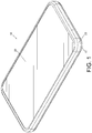
FIG. 1 is a diagram showing a communication device according to an embodiment of the present invention; -
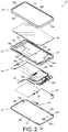
FIG. 2 is an exploded view of the communication device according to an embodiment of the present invention; -
FIG. 3 is an exploded view of a main body and an auxiliary component of the communication device according to an embodiment of the present invention; -
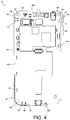
FIG. 4 is a diagram showing arrangement of a mother board and antennas according to an embodiment of the present invention; -
FIG. 5 is a partial view of an assembly of a housing, the main body and a frame according to an embodiment of the present invention, for illustrating a portion of the antenna being extended beyond a side part of the housing; -
FIG. 6 is a diagram showing the mother board of the communication device electrically connected to the housing and the antenna according to an embodiment of the present invention; -
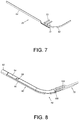
FIG. 7 is a diagram showing one of the antennas according to an embodiment of the present invention; and -
FIG. 8 is a diagram showing another one of the antennas according to an embodiment of the present invention. - As shown in
FIG. 1 andFIG. 2 , acommunication device 10 of the present invention comprises amain body 12, ahousing 14, amother board 16, afirst antenna 18 and adisplay module 20. Preferably, thecommunication device 10 further comprises aframe 22, anauxiliary component 24, asecond antenna 26, athird antenna 28 and abattery 30. - The
main body 12 is made of a non-metallic material, such as plastic. A rim is formed on themain body 12. The rim comprises a plurality of rim parts. In the present embodiment, the rim comprises a pair offirst rim part second rim part space 36 is defined by therim parts first rim part 32a (or 32b) is greater than a length of thesecond rim part 34a (or 34b) . - The
housing 14 can be mounted to themain body 12, and is configured to cover most of themother board 16 and thebattery 30 for protecting related electronic components of thecommunication device 10. Thehousing 14 can be made of a metal material or a non-metallic material (such as plastic). In the present embodiment, thehousing 14 is a back cover, and thehousing 14 is made of a metal material. Thehousing 14 can function as a ground of themother board 16. Furthermore, thehousing 14 comprises aninner surface 37 and a plurality of side parts located around theinner surface 37. For example, the side parts are a pair offirst side parts second side parts inner surface 37 can have at least one ground area. In the present embodiment, theinner surface 37 hasground areas ground areas - The
mother board 16 is correspondingly arranged in thespace 36 defined by therim parts main body 12. In particular, themother board 16 comprises a plurality of side parts. For example, themother board 16 comprises a pair offirst side parts second side parts 46a, 4 6b. In the present embodiment, themother board 16 is located between themain body 12 and thehousing 14, and is completely covered by thehousing 14. - The
display module 20 is configured to display electronic information of thecommunication device 10, and thedisplay module 20 can be a touch display module. Since the display module is well known to those skilled in the art, no further illustration is provided. In the present embodiment, thedisplay module 20 is located between themain body 12 and theframe 22, and electrically connected to themother board 16. - The
frame 22 can be mounted to themain body 12, such that themain body 12 is located between theframe 22 and thehousing 14. Theframe 22 is a major exterior part of thecommunication device 10, and theframe 22 can be decorated by various surface treatments. Preferably, an outer dimension of theframe 22 is greater than an outer dimension of themain body 12, and an outer dimension of thehousing 14 is smaller than or equal to the outer dimension of themain body 12. In particular, theframe 22 comprises a plurality of frame parts, such as a pair offirst frame parts second frame parts space 52 is defined by theframe parts main body 12 and thedisplay module 20 therein. Preferably, theframe 22 is made of a non-metallic material, such as plastic. - The
battery 30 is configured to provide electricity to thecommunication device 10. For example, thebattery 30 is electrically connected to themother board 16 for providing electricity. - The
first antenna 18, thesecond antenna 26 and thethird antenna 28 can be formed on themain body 12 as flexible printed circuit boards, or formed on themain body 12 by laser direct structuring, metal printing or metal stamping. - As shown in
FIG. 2 andFIG. 3 , theauxiliary component 24 is adjacent to themain body 12. Connection between theauxiliary component 24 and themain body 12 can be implemented by injection molding, ultrasonic welding or hot melting. Preferably, theauxiliary component 24 is attached to a second side of the main body 12 (different from the first side of the main body 12). Wherein, theauxiliary component 24 is made of a metal material. In particular, if thedisplay module 20 comprises a metal shielding mask, thedisplay module 20 can be electrically connected to theauxiliary component 24 through an elastic metal piece or other conductive material. Theauxiliary component 24 comprises a plurality of side parts corresponding to therim parts main body 12. For example, theauxiliary component 24 comprises a pair offirst side parts second side parts main body 12 comprises a separatingmember 58 configured to separate theauxiliary component 24 from themother board 16. Wherein, since theauxiliary component 24 is made of a metal material, theauxiliary component 24 is capable of improving structure strength of themain body 12. Theauxiliary component 24 can also help the mother board to dissipate heat. In addition, when thehousing 14 is made of a plastic material, theauxiliary component 24 can function as a ground of themother board 16. For example, themother board 16 can be electrically connected to theauxiliary component 24 through an elastic metal piece or other conductive material. On the other hand, both thehousing 14 and theauxiliary component 24 can be made of the metal material for being utilized as grounds of themother board 16. In addition, thehousing 14, themother board 16 and one of theantennas - As shown in
FIG. 4 , a length of thefirst side part 44b of themother board 16 is greater than a length of thesecond side part 46a (or 46b) of themother board 16. In addition, there are corners between theside parts mother board 16. For example, afirst corner 60, asecond corner 62 and athird corner 64 are formed at turning positions of theside parts mother board 16. On the other hand, thefirst antenna 18, thesecond antenna 26 and thethird antenna 28 can be respectively located adjacent to thefirst corner 60, thesecond corner 62 and thethird corner 64. In other words, a portion of each antenna is located adjacent to a corresponding corner of themother board 16. Wherein, thethird antenna 28 can be a GPS (Global Positioning System) antenna or WIFI antenna. - Moreover, each of the
first antenna 18, thesecond antenna 26 and thethird antenna 28 has a feed terminal and a ground terminal. In the present embodiment, thefirst antenna 18 has afeed terminal 66 and aground terminal 68 respectively electrically connected to themother board 16; thesecond antenna 26 has afeed terminal 70 and aground terminal 72 respectively electrically connected to themother board 16; and thethird antenna 28 has afeed terminal 74 and aground terminal 76 respectively electrically connected to themother board 16. - The antennas can comprise a plurality of radiation parts. For example, the
first antenna 18 has afirst radiation part 78 and asecond radiation part 80. Thefirst radiation part 78 is configured to transmit or receive a high frequency signal. Thesecond radiation part 80 is configured to transmit or receive a low frequency signal. Wherein, thesecond radiation part 80 of thefirst antenna 18 corresponds to thefirst side part 44b of themother board 16, and thefirst radiation part 78 of thefirst antenna 18 corresponds to thesecond side part 46b of themother board 16. A length of thefirst radiation part 78 is smaller than a length of thesecond radiation part 80. Similarly, thesecond antenna 26 has afirst radiation part 82 and asecond radiation part 84. Thefirst radiation part 82 is configured to transmit or receive a high frequency signal. Thesecond radiation part 84 is configured to transmit or receive a low frequency signal. Wherein, thesecond radiation part 84 of thesecond antenna 26 corresponds to thefirst side part 44b of themother board 16, and thefirst radiation part 82 of thesecond antenna 26 corresponds to thesecond side part 46a of themother board 16. A length of thefirst radiation part 82 is smaller than a length of thesecond radiation part 84. - In addition, the
third antenna 28 has afirst radiation part 86 and asecond radiation part 88. Wherein, thesecond radiation part 88 of thethird antenna 28 corresponds to thefirst side part 44a of themother board 16, and thefirst radiation part 86 of thethird antenna 28 corresponds to thesecond side part 46a of themother board 16. - As shown in
FIG. 5 , thehousing 14 can be mounted to themain body 12 by fastening or screwing. On the other hand, theframe 22 can be mounted to themain body 12 by fastening, ultrasonic welding or hot melting. The mounting methods between thehousing 14, themain body 12 and theframe 22 are not limited thereto. In addition, since the outer dimension of theframe 22 is greater than the outer dimension of themain body 12, thespace 52 of theframe 22 is capable of accommodating themain body 12. Moreover, since the outer dimension of thehousing 14 is smaller than or equal to the outer dimension of themain body 12, theframe 22 is also capable of accommodating a portion of the housing 14 (please referFIG. 1 ). - Portions of the
first antenna 18, thesecond antenna 26 and thethird antenna 28 are arranged adjacent to themain body 12. For simplification, only thefirst antenna 18 is illustrated. Aportion 90 of thefirst antenna 18 is adjacent to themain body 12. In the present embodiment, theportion 90 of thefirst antenna 18 is attached to one of the rim parts of themain body 12, such as attaching to thesecond rim part 34b. An orthogonal projection of thehousing 14 onto themain body 12 defines a covering range. Preferably, theportion 90 of the first antenna 18 (or the whole first antenna 18) is located outside the covering range of thehousing 14. As shown inFIG. 5 , theportion 90 of thefirst antenna 18 is located in an area outside the covering range of thehousing 14. Briefly, theportion 90 of thefirst antenna 18 is not covered by thehousing 14. In the present embodiment, theportion 90 of thefirst antenna 18 is extended a distance D beyond a side part of the housing 14 (such as thesecond side part 40b). Preferably, theportion 90 of thefirst antenna 18 is located between thesecond frame part 50b of theframe 22 and thesecond rim part 34b of themain body 12. Theportion 90 of thefirst antenna 18 can be thefirst radiation part 78 or thesecond radiation part 80 of thefirst antenna 18. In the present embodiment, theportion 90 of thefirst antenna 18 is thefirst radiation part 78 of thefirst antenna 18, but the present invention is not limited thereto. As such, a main radiation part of thefirst antenna 18 is located outside the covering range of thehousing 14. - Similarly, a portion of each of the
second antenna 26 and the third antenna 28 (such as a first radiation part or a second radiation part) is also extended a distance beyond thehousing 14 to be located outside the covering range of thehousing 14, such that a main radiation part of each of thesecond antenna 26 and thethird antenna 28 is located outside the covering range of thehousing 14. For simplification, no further illustration is provided. - In
FIG. 6 , only thesecond antenna 26 and thethird antenna 28 are illustrated. Thefeed terminal 70 of thesecond antenna 26 and thefeed terminal 74 of thethird antenna 28 can be respectively electrically connected to themother board 16 through elastic metal pieces or other conductive material. Similarly, theground terminal 72 of the second antenna 26 (not shown inFIG. 6 ) and theground terminal 76 of the third antenna 28 (not shown inFIG. 6 ) can be respectively electrically connected to themother board 16 through elastic metal pieces or other conductive material. On the other hand, theground terminals first antenna 18, thesecond antenna 26 and thethird antenna 28 can also be respectively electrically connected to thecorresponding ground areas housing 14 by themother board 16 through an elastic metal piece or other conductive material. - As shown in
FIG. 7 , thesecond antenna 26 comprises thefirst radiation part 82 and thesecond radiation part 84. Thefeed terminal 70 and theground terminal 72 are located between thefirst radiation part 82 and thesecond radiation part 84. - As shown in
FIG. 8 , thesecond radiation part 80 of thefirst antenna 18 comprises afirst conductor 92 and asecond conductor 94 coupled to thefirst conductor 92. Thesecond conductor 94 has afirst slit 96 and asecond slit 98. Wherein, thefirst slit 96 is arranged along a longitudinal direction of thesecond radiation part 80, and thesecond slit 98 is turned relative to thefirst slit 96 and communicated with thefirst slit 96. Agap 100 is formed between thefirst radiation part 78 and thesecond radiation part 80 of thefirst antenna 18, and thefirst radiation part 78 has athird slit 102 arranged along a longitudinal direction of thefirst radiation part 78. According to the above arrangement, efficiency of signal transmission and reception of thefirst antenna 18 can be improved.
Claims (15)
- A communication device (10), comprising:a main body (12) formed with a rim;a mother board (16) arranged at a first side of the main body (12);characterized by:a housing (14) mounted on the main body (12) and configured to cover the mother board (16), an orthogonal projection of the housing (14) onto the main body (12) defining a covering range; anda first antenna (18) electrically connected to the mother board (16) and arranged along the rim of the main body (12), wherein at least one portion of the first antenna (18) is located outside the covering range of the housing (14).
- The communication device of claim 1, characterized in that the mother board (16) is located between the main body (12) and the housing (14).
- The communication device of claim 1 or 2, characterized in that the rim of the main body (12) comprises a plurality of rim parts (32a, 32b, 34a, 34b), the mother board (16) is correspondingly arranged between the rim parts (32a, 32b, 34a, 34b), the first antenna (18) comprises a feed terminal (66) electrically connected to the mother board (16), and a portion of the first antenna (18) is attached to one of the rim parts (34b) of the main body (12).
- The communication device of any of claims 1-3, characterized in that the housing (14) comprises a plurality of side parts (38a, 38b, 40a, 40b), the at least one portion of the first antenna (18) is extended beyond one of the side parts (40b) of the housing (14) to be located outside the covering range of the housing (14) .
- The communication device of claim 4, further characterized by a frame (22) mounted to the main body (12), wherein the main body (12) is located between the frame (22) and the housing (14), the frame (22) comprises a plurality of frame parts (48a, 48b, 50a, 50b) defining a space (52) for accommodating the main body (12), the at least one portion of the first antenna (18) is located between the frame (22) and the main body (12), an outer dimension of the frame (22) is greater than an outer dimension of the main body (12), and an outer dimension of the housing (14) is smaller than or equal to the outer dimension of the main body (12).
- The communication device of any of claims 1-5, characterized in that the at least one portion of the first antenna (18) comprises one of a first radiation part (78) and a second radiation part (80), the first radiation part (78) is configured to transmit or receive a high frequency signal, the second radiation part (80) is configured to transmit or receive a low frequency signal.
- The communication device of claim 6, characterized in that the second radiation part (80) comprises a first conductor (92) and a second conductor (94) coupled to the first conductor (92), the second conductor (94) has a first slit (96) and a second slit (98), the first slit (96) is arranged along a longitudinal direction of the second conductor (94), the second slit (98) is turned relative to the first slit (96) and communicated with the first slit (96), a gap (100) is formed between the first radiation part (78) and the second radiation part (80), the first radiation part (78) has a third slit (102) arranged along a longitudinal direction of the first radiation part (78).
- The communication device of claim 6 or 7, characterized in that a length of the first radiation part (78) is smaller than a length of the second radiation part (80).
- The communication device of any of claims 1-8, characterized in that a portion of the first antenna (18) is located adjacent to a corner (60) of the mother board (16).
- The communication device of claim 3, further characterized by an auxiliary component (24) attached to a second side of the main body (12), wherein the auxiliary (24) component is made of a metal material and comprises a plurality of side parts (54a, 54b, 56a, 56b) corresponding to the rim parts (32a, 32b, 34a, 34b) of the main body (12).
- The communication device of any of claims 1-10, characterized in that the housing (14) is a back cover, the housing (14) is made of a metal or plastic material, when the housing (14) is made of a metal material, the housing (14) functions as a ground of the mother board (16).
- The communication device of claim 9, further characterized by a second antenna (26) and a third antenna (28), wherein each of the second antenna (26) and the third antenna (28) comprises a feed terminal (70, 74) electrically connected to the mother board (16), a portion of each of the second antenna (26) and the third antenna (28) is extended beyond the housing (14) to be located outside the covering range of the housing (14).
- The communication device of claim 12, characterized in that portions of the second antenna (26) and the third antenna (28) are respectively located adjacent to another two corners (62, 64) of the mother board (16).
- An antenna assembly for a communication device (10), comprising:a mother board (16); andcharacterized by:an antenna (18, 26, 28) comprising a feed terminal (66, 70, 74) electrically connected to the mother board (16), the antenna (18, 26, 28) being arranged along a side part (44a, 44b, 46a, 46b) of the mother board (16);wherein the mother board (16) is covered by a back cover (14) of the communication device (10), and a portion of the antenna (18, 26, 28) is not covered by the back cover (14).
- The antenna assembly of claim 14, characterized in that the back cover (14) is made of a metal material.
Applications Claiming Priority (1)
| Application Number | Priority Date | Filing Date | Title |
|---|---|---|---|
| TW105119383A TWI631768B (en) | 2016-06-20 | 2016-06-20 | Communication device and antenna parts thereof |
Publications (2)
| Publication Number | Publication Date |
|---|---|
| EP3261173A1 true EP3261173A1 (en) | 2017-12-27 |
| EP3261173B1 EP3261173B1 (en) | 2019-02-20 |
Family
ID=57570349
Family Applications (1)
| Application Number | Title | Priority Date | Filing Date |
|---|---|---|---|
| EP16204573.6A Not-in-force EP3261173B1 (en) | 2016-06-20 | 2016-12-16 | Communication device and antenna assembly thereof |
Country Status (4)
| Country | Link |
|---|---|
| US (1) | US10403966B2 (en) |
| EP (1) | EP3261173B1 (en) |
| JP (1) | JP6309073B2 (en) |
| TW (1) | TWI631768B (en) |
Cited By (2)
| Publication number | Priority date | Publication date | Assignee | Title |
|---|---|---|---|---|
| CN108336475A (en) * | 2018-01-29 | 2018-07-27 | 广东欧珀移动通信有限公司 | Middle frame assembly, electronic equipment and assembling method thereof |
| EP3855875A4 (en) * | 2018-11-12 | 2021-12-01 | Samsung Electronics Co., Ltd. | ELECTRONIC DEVICE INCLUDING A HEAT DISSIPATION STRUCTURE |
Families Citing this family (15)
| Publication number | Priority date | Publication date | Assignee | Title |
|---|---|---|---|---|
| CN107967026B (en) * | 2017-11-23 | 2019-10-25 | Oppo广东移动通信有限公司 | Antenna assembly, terminal equipment and method for improving antenna radiation performance |
| KR20190098607A (en) * | 2018-02-14 | 2019-08-22 | 엘지전자 주식회사 | Mobile terminal including metal case and method of manufacturing metal case |
| CN112385090B (en) | 2018-07-06 | 2024-11-01 | 株式会社村田制作所 | Antenna module and communication device |
| KR102721373B1 (en) | 2019-01-28 | 2024-10-24 | 삼성전자주식회사 | Electronic device having a thermal spreading structure |
| ES2953593T3 (en) * | 2019-02-19 | 2023-11-14 | Samsung Electronics Co Ltd | Electronic device that includes an antenna |
| KR102699068B1 (en) | 2019-08-06 | 2024-08-27 | 삼성전자주식회사 | Antenna and electronic device including the same |
| TWI704396B (en) * | 2019-08-15 | 2020-09-11 | 啟碁科技股份有限公司 | Electronic display device |
| CN113451740A (en) * | 2020-03-25 | 2021-09-28 | 中兴通讯股份有限公司 | Electronic equipment and shell thereof |
| US11363745B1 (en) * | 2020-07-07 | 2022-06-14 | Waymo Llc | Housing for display electromagnetic shielding and electrostatic grounding |
| US11201423B2 (en) * | 2020-07-15 | 2021-12-14 | Google Llc | Card connector assemblies with integrated component shielding |
| CN111954409B (en) * | 2020-08-13 | 2021-09-14 | 东莞美景科技有限公司 | Preparation method of shell with built-in antenna |
| TWI819618B (en) * | 2022-05-23 | 2023-10-21 | 和碩聯合科技股份有限公司 | Electronic device |
| CN115224475B (en) * | 2022-08-03 | 2024-04-16 | 荣耀终端有限公司 | Electronic equipment |
| TWI823588B (en) * | 2022-09-28 | 2023-11-21 | 華碩電腦股份有限公司 | Wideband antenna structure |
| US12217107B2 (en) | 2023-01-25 | 2025-02-04 | Google Llc | Integrated memory card ejector and sensor ports |
Citations (5)
| Publication number | Priority date | Publication date | Assignee | Title |
|---|---|---|---|---|
| US20070241971A1 (en) * | 2006-04-13 | 2007-10-18 | Kabushiki Kaisha Toshiba | Mobile communication terminal |
| US20080316121A1 (en) * | 2007-06-21 | 2008-12-25 | Hobson Phillip M | Wireless handheld electronic device |
| US8054231B2 (en) | 2008-05-06 | 2011-11-08 | Samsung Electronics Co., Ltd. | Mobile terminal having metal case and antenna structure |
| US20130069836A1 (en) * | 2011-09-21 | 2013-03-21 | Sony Mobile Communications Japan, Inc. | Wireless communication apparatus |
| US20150245513A1 (en) * | 2014-02-21 | 2015-08-27 | Samsung Electronics Co., Ltd. | Electronic device and method for manufacturing housing of the electronic device |
Family Cites Families (22)
| Publication number | Priority date | Publication date | Assignee | Title |
|---|---|---|---|---|
| JP2507459B2 (en) | 1987-08-07 | 1996-06-12 | 日本電信電話株式会社 | Optical fiber connector core fixing method |
| JPS6440910U (en) | 1987-09-07 | 1989-03-10 | ||
| JP3192085B2 (en) * | 1996-03-13 | 2001-07-23 | 株式会社日立国際電気 | Small antenna |
| US6552686B2 (en) * | 2001-09-14 | 2003-04-22 | Nokia Corporation | Internal multi-band antenna with improved radiation efficiency |
| JP4649634B2 (en) | 2005-06-30 | 2011-03-16 | 独立行政法人情報通信研究機構 | Multiband monopole antenna |
| JP4762126B2 (en) * | 2006-12-20 | 2011-08-31 | 株式会社東芝 | Electronics |
| JP4881247B2 (en) * | 2007-07-13 | 2012-02-22 | 株式会社東芝 | Electronic device and manufacturing method thereof |
| KR20120018329A (en) | 2009-04-21 | 2012-03-02 | 몰렉스 인코포레이티드 | Three dimensional antenna |
| CN102290632A (en) * | 2010-06-15 | 2011-12-21 | 深圳富泰宏精密工业有限公司 | Electronic device shell and manufacturing method thereof |
| TWI518983B (en) * | 2010-10-28 | 2016-01-21 | 宏達國際電子股份有限公司 | Hand-held device |
| JP5794174B2 (en) | 2012-02-24 | 2015-10-14 | カシオ計算機株式会社 | ANTENNA DEVICE AND ELECTRONIC DEVICE |
| KR101978956B1 (en) * | 2012-07-27 | 2019-05-16 | 엘지전자 주식회사 | Mobile terminal |
| KR102025706B1 (en) * | 2013-01-30 | 2019-09-26 | 삼성전자주식회사 | Antenna device for portable terminal |
| KR102118381B1 (en) * | 2013-03-06 | 2020-06-04 | 엘지전자 주식회사 | Mobile terminal |
| KR102119660B1 (en) * | 2013-10-17 | 2020-06-08 | 엘지전자 주식회사 | Mobile terminal |
| KR102184621B1 (en) * | 2014-02-21 | 2020-11-30 | 삼성전자주식회사 | Mobile communication terminal with radiat-heat sheet |
| US9203141B1 (en) * | 2014-06-11 | 2015-12-01 | King Slide Technology Co., Ltd. | Communication device and antenna thereof |
| KR102138910B1 (en) * | 2014-06-23 | 2020-07-28 | 삼성전자주식회사 | Electronic device with ring type antenna |
| KR102129799B1 (en) * | 2014-09-19 | 2020-07-03 | 엘지전자 주식회사 | Mobile terminal |
| CN105530774A (en) * | 2014-09-29 | 2016-04-27 | 深圳富泰宏精密工业有限公司 | Shell and electronic device provided with shell |
| US9343802B2 (en) * | 2014-10-15 | 2016-05-17 | King Slide Technology Co., Ltd. | Communication device and antenna thereof |
| KR20160067541A (en) * | 2014-12-04 | 2016-06-14 | 엘지전자 주식회사 | Antenna module and mobile terminal using the same |
-
2016
- 2016-06-20 TW TW105119383A patent/TWI631768B/en active
- 2016-11-07 US US15/344,604 patent/US10403966B2/en not_active Expired - Fee Related
- 2016-12-01 JP JP2016233734A patent/JP6309073B2/en not_active Expired - Fee Related
- 2016-12-16 EP EP16204573.6A patent/EP3261173B1/en not_active Not-in-force
Patent Citations (5)
| Publication number | Priority date | Publication date | Assignee | Title |
|---|---|---|---|---|
| US20070241971A1 (en) * | 2006-04-13 | 2007-10-18 | Kabushiki Kaisha Toshiba | Mobile communication terminal |
| US20080316121A1 (en) * | 2007-06-21 | 2008-12-25 | Hobson Phillip M | Wireless handheld electronic device |
| US8054231B2 (en) | 2008-05-06 | 2011-11-08 | Samsung Electronics Co., Ltd. | Mobile terminal having metal case and antenna structure |
| US20130069836A1 (en) * | 2011-09-21 | 2013-03-21 | Sony Mobile Communications Japan, Inc. | Wireless communication apparatus |
| US20150245513A1 (en) * | 2014-02-21 | 2015-08-27 | Samsung Electronics Co., Ltd. | Electronic device and method for manufacturing housing of the electronic device |
Cited By (3)
| Publication number | Priority date | Publication date | Assignee | Title |
|---|---|---|---|---|
| CN108336475A (en) * | 2018-01-29 | 2018-07-27 | 广东欧珀移动通信有限公司 | Middle frame assembly, electronic equipment and assembling method thereof |
| EP3855875A4 (en) * | 2018-11-12 | 2021-12-01 | Samsung Electronics Co., Ltd. | ELECTRONIC DEVICE INCLUDING A HEAT DISSIPATION STRUCTURE |
| US11910516B2 (en) | 2018-11-12 | 2024-02-20 | Samsung Electronics Co., Ltd | Electronic device including heat dissipation structure |
Also Published As
| Publication number | Publication date |
|---|---|
| TWI631768B (en) | 2018-08-01 |
| EP3261173B1 (en) | 2019-02-20 |
| TW201801396A (en) | 2018-01-01 |
| US20170365912A1 (en) | 2017-12-21 |
| US10403966B2 (en) | 2019-09-03 |
| JP2017229055A (en) | 2017-12-28 |
| JP6309073B2 (en) | 2018-04-11 |
Similar Documents
| Publication | Publication Date | Title |
|---|---|---|
| EP3261173B1 (en) | Communication device and antenna assembly thereof | |
| KR101658821B1 (en) | Shield can of mobile terminal | |
| US10056676B2 (en) | Antenna device and electronic appliance | |
| US9343802B2 (en) | Communication device and antenna thereof | |
| EP3340584A1 (en) | Bracket assembly for functional component for mobile terminal | |
| US20130257662A1 (en) | Antenna device of mobile terminal | |
| EP2698868B1 (en) | Internal antenna of mobile terminal | |
| EP1633015B1 (en) | Sealing member and sealing structure of electronic circuit unit | |
| CN109904589B (en) | Wireless communication module | |
| US20070121307A1 (en) | EMI/RFI shield for electronic device | |
| JP2019106690A (en) | Wireless communication device | |
| US10468749B2 (en) | Mobile display terminal | |
| KR20160055573A (en) | Antenna module and electronic device including the same | |
| EP3012904B1 (en) | Communication device and antenna thereof | |
| JP2011024022A (en) | Mobile walkie-talkie | |
| CN111900527B (en) | Antenna structure and electronic equipment | |
| EP2958189B1 (en) | Communication device and antenna thereof | |
| CN107528118B (en) | Communication device and antenna assembly thereof | |
| JP7130470B2 (en) | wireless communication device | |
| JP2011023683A (en) | Electronic circuit module | |
| EP1732161A1 (en) | Internal antenna apparatus and mobile communication terminal having same | |
| JP4788623B2 (en) | Wireless device | |
| US20120014076A1 (en) | Card-type electronic circuit module | |
| US20090303151A1 (en) | Low profile gps antenna assembly | |
| WO2013069692A1 (en) | Communication module, connector, and communication module provided with connector |
Legal Events
| Date | Code | Title | Description |
|---|---|---|---|
| PUAI | Public reference made under article 153(3) epc to a published international application that has entered the european phase |
Free format text: ORIGINAL CODE: 0009012 |
|
| STAA | Information on the status of an ep patent application or granted ep patent |
Free format text: STATUS: THE APPLICATION HAS BEEN PUBLISHED |
|
| AK | Designated contracting states |
Kind code of ref document: A1 Designated state(s): AL AT BE BG CH CY CZ DE DK EE ES FI FR GB GR HR HU IE IS IT LI LT LU LV MC MK MT NL NO PL PT RO RS SE SI SK SM TR |
|
| AX | Request for extension of the european patent |
Extension state: BA ME |
|
| STAA | Information on the status of an ep patent application or granted ep patent |
Free format text: STATUS: REQUEST FOR EXAMINATION WAS MADE |
|
| 17P | Request for examination filed |
Effective date: 20180622 |
|
| RBV | Designated contracting states (corrected) |
Designated state(s): AL AT BE BG CH CY CZ DE DK EE ES FI FR GB GR HR HU IE IS IT LI LT LU LV MC MK MT NL NO PL PT RO RS SE SI SK SM TR |
|
| RIC1 | Information provided on ipc code assigned before grant |
Ipc: H01Q 21/28 20060101ALN20180808BHEP Ipc: H01Q 1/38 20060101ALI20180808BHEP Ipc: H01Q 9/42 20060101ALN20180808BHEP Ipc: H01Q 1/24 20060101AFI20180808BHEP |
|
| GRAP | Despatch of communication of intention to grant a patent |
Free format text: ORIGINAL CODE: EPIDOSNIGR1 |
|
| STAA | Information on the status of an ep patent application or granted ep patent |
Free format text: STATUS: GRANT OF PATENT IS INTENDED |
|
| INTG | Intention to grant announced |
Effective date: 20180917 |
|
| GRAS | Grant fee paid |
Free format text: ORIGINAL CODE: EPIDOSNIGR3 |
|
| GRAA | (expected) grant |
Free format text: ORIGINAL CODE: 0009210 |
|
| STAA | Information on the status of an ep patent application or granted ep patent |
Free format text: STATUS: THE PATENT HAS BEEN GRANTED |
|
| AK | Designated contracting states |
Kind code of ref document: B1 Designated state(s): AL AT BE BG CH CY CZ DE DK EE ES FI FR GB GR HR HU IE IS IT LI LT LU LV MC MK MT NL NO PL PT RO RS SE SI SK SM TR |
|
| REG | Reference to a national code |
Ref country code: GB Ref legal event code: FG4D |
|
| REG | Reference to a national code |
Ref country code: CH Ref legal event code: EP |
|
| REG | Reference to a national code |
Ref country code: DE Ref legal event code: R096 Ref document number: 602016010094 Country of ref document: DE |
|
| REG | Reference to a national code |
Ref country code: AT Ref legal event code: REF Ref document number: 1099401 Country of ref document: AT Kind code of ref document: T Effective date: 20190315 |
|
| REG | Reference to a national code |
Ref country code: IE Ref legal event code: FG4D |
|
| REG | Reference to a national code |
Ref country code: LT Ref legal event code: MG4D |
|
| REG | Reference to a national code |
Ref country code: NL Ref legal event code: MP Effective date: 20190220 |
|
| PG25 | Lapsed in a contracting state [announced via postgrant information from national office to epo] |
Ref country code: FI Free format text: LAPSE BECAUSE OF FAILURE TO SUBMIT A TRANSLATION OF THE DESCRIPTION OR TO PAY THE FEE WITHIN THE PRESCRIBED TIME-LIMIT Effective date: 20190220 Ref country code: PT Free format text: LAPSE BECAUSE OF FAILURE TO SUBMIT A TRANSLATION OF THE DESCRIPTION OR TO PAY THE FEE WITHIN THE PRESCRIBED TIME-LIMIT Effective date: 20190620 Ref country code: SE Free format text: LAPSE BECAUSE OF FAILURE TO SUBMIT A TRANSLATION OF THE DESCRIPTION OR TO PAY THE FEE WITHIN THE PRESCRIBED TIME-LIMIT Effective date: 20190220 Ref country code: NO Free format text: LAPSE BECAUSE OF FAILURE TO SUBMIT A TRANSLATION OF THE DESCRIPTION OR TO PAY THE FEE WITHIN THE PRESCRIBED TIME-LIMIT Effective date: 20190520 Ref country code: LT Free format text: LAPSE BECAUSE OF FAILURE TO SUBMIT A TRANSLATION OF THE DESCRIPTION OR TO PAY THE FEE WITHIN THE PRESCRIBED TIME-LIMIT Effective date: 20190220 |
|
| PG25 | Lapsed in a contracting state [announced via postgrant information from national office to epo] |
Ref country code: HR Free format text: LAPSE BECAUSE OF FAILURE TO SUBMIT A TRANSLATION OF THE DESCRIPTION OR TO PAY THE FEE WITHIN THE PRESCRIBED TIME-LIMIT Effective date: 20190220 Ref country code: RS Free format text: LAPSE BECAUSE OF FAILURE TO SUBMIT A TRANSLATION OF THE DESCRIPTION OR TO PAY THE FEE WITHIN THE PRESCRIBED TIME-LIMIT Effective date: 20190220 Ref country code: BG Free format text: LAPSE BECAUSE OF FAILURE TO SUBMIT A TRANSLATION OF THE DESCRIPTION OR TO PAY THE FEE WITHIN THE PRESCRIBED TIME-LIMIT Effective date: 20190520 Ref country code: NL Free format text: LAPSE BECAUSE OF FAILURE TO SUBMIT A TRANSLATION OF THE DESCRIPTION OR TO PAY THE FEE WITHIN THE PRESCRIBED TIME-LIMIT Effective date: 20190220 Ref country code: GR Free format text: LAPSE BECAUSE OF FAILURE TO SUBMIT A TRANSLATION OF THE DESCRIPTION OR TO PAY THE FEE WITHIN THE PRESCRIBED TIME-LIMIT Effective date: 20190521 Ref country code: IS Free format text: LAPSE BECAUSE OF FAILURE TO SUBMIT A TRANSLATION OF THE DESCRIPTION OR TO PAY THE FEE WITHIN THE PRESCRIBED TIME-LIMIT Effective date: 20190620 Ref country code: LV Free format text: LAPSE BECAUSE OF FAILURE TO SUBMIT A TRANSLATION OF THE DESCRIPTION OR TO PAY THE FEE WITHIN THE PRESCRIBED TIME-LIMIT Effective date: 20190220 |
|
| REG | Reference to a national code |
Ref country code: AT Ref legal event code: MK05 Ref document number: 1099401 Country of ref document: AT Kind code of ref document: T Effective date: 20190220 |
|
| PG25 | Lapsed in a contracting state [announced via postgrant information from national office to epo] |
Ref country code: EE Free format text: LAPSE BECAUSE OF FAILURE TO SUBMIT A TRANSLATION OF THE DESCRIPTION OR TO PAY THE FEE WITHIN THE PRESCRIBED TIME-LIMIT Effective date: 20190220 Ref country code: SK Free format text: LAPSE BECAUSE OF FAILURE TO SUBMIT A TRANSLATION OF THE DESCRIPTION OR TO PAY THE FEE WITHIN THE PRESCRIBED TIME-LIMIT Effective date: 20190220 Ref country code: IT Free format text: LAPSE BECAUSE OF FAILURE TO SUBMIT A TRANSLATION OF THE DESCRIPTION OR TO PAY THE FEE WITHIN THE PRESCRIBED TIME-LIMIT Effective date: 20190220 Ref country code: DK Free format text: LAPSE BECAUSE OF FAILURE TO SUBMIT A TRANSLATION OF THE DESCRIPTION OR TO PAY THE FEE WITHIN THE PRESCRIBED TIME-LIMIT Effective date: 20190220 Ref country code: AL Free format text: LAPSE BECAUSE OF FAILURE TO SUBMIT A TRANSLATION OF THE DESCRIPTION OR TO PAY THE FEE WITHIN THE PRESCRIBED TIME-LIMIT Effective date: 20190220 Ref country code: RO Free format text: LAPSE BECAUSE OF FAILURE TO SUBMIT A TRANSLATION OF THE DESCRIPTION OR TO PAY THE FEE WITHIN THE PRESCRIBED TIME-LIMIT Effective date: 20190220 Ref country code: CZ Free format text: LAPSE BECAUSE OF FAILURE TO SUBMIT A TRANSLATION OF THE DESCRIPTION OR TO PAY THE FEE WITHIN THE PRESCRIBED TIME-LIMIT Effective date: 20190220 Ref country code: ES Free format text: LAPSE BECAUSE OF FAILURE TO SUBMIT A TRANSLATION OF THE DESCRIPTION OR TO PAY THE FEE WITHIN THE PRESCRIBED TIME-LIMIT Effective date: 20190220 |
|
| REG | Reference to a national code |
Ref country code: DE Ref legal event code: R097 Ref document number: 602016010094 Country of ref document: DE |
|
| PG25 | Lapsed in a contracting state [announced via postgrant information from national office to epo] |
Ref country code: SM Free format text: LAPSE BECAUSE OF FAILURE TO SUBMIT A TRANSLATION OF THE DESCRIPTION OR TO PAY THE FEE WITHIN THE PRESCRIBED TIME-LIMIT Effective date: 20190220 Ref country code: PL Free format text: LAPSE BECAUSE OF FAILURE TO SUBMIT A TRANSLATION OF THE DESCRIPTION OR TO PAY THE FEE WITHIN THE PRESCRIBED TIME-LIMIT Effective date: 20190220 |
|
| PLBE | No opposition filed within time limit |
Free format text: ORIGINAL CODE: 0009261 |
|
| STAA | Information on the status of an ep patent application or granted ep patent |
Free format text: STATUS: NO OPPOSITION FILED WITHIN TIME LIMIT |
|
| PG25 | Lapsed in a contracting state [announced via postgrant information from national office to epo] |
Ref country code: AT Free format text: LAPSE BECAUSE OF FAILURE TO SUBMIT A TRANSLATION OF THE DESCRIPTION OR TO PAY THE FEE WITHIN THE PRESCRIBED TIME-LIMIT Effective date: 20190220 |
|
| REG | Reference to a national code |
Ref country code: DE Ref legal event code: R082 Ref document number: 602016010094 Country of ref document: DE Representative=s name: STRAUS, ALEXANDER, DIPL.-CHEM.UNIV. DR.PHIL., DE Ref country code: DE Ref legal event code: R082 Ref document number: 602016010094 Country of ref document: DE Representative=s name: 2K PATENT- UND RECHTSANWAELTE PARTNERSCHAFT MB, DE |
|
| 26N | No opposition filed |
Effective date: 20191121 |
|
| PG25 | Lapsed in a contracting state [announced via postgrant information from national office to epo] |
Ref country code: SI Free format text: LAPSE BECAUSE OF FAILURE TO SUBMIT A TRANSLATION OF THE DESCRIPTION OR TO PAY THE FEE WITHIN THE PRESCRIBED TIME-LIMIT Effective date: 20190220 |
|
| PG25 | Lapsed in a contracting state [announced via postgrant information from national office to epo] |
Ref country code: TR Free format text: LAPSE BECAUSE OF FAILURE TO SUBMIT A TRANSLATION OF THE DESCRIPTION OR TO PAY THE FEE WITHIN THE PRESCRIBED TIME-LIMIT Effective date: 20190220 |
|
| REG | Reference to a national code |
Ref country code: CH Ref legal event code: PL |
|
| REG | Reference to a national code |
Ref country code: BE Ref legal event code: MM Effective date: 20191231 |
|
| PG25 | Lapsed in a contracting state [announced via postgrant information from national office to epo] |
Ref country code: MC Free format text: LAPSE BECAUSE OF FAILURE TO SUBMIT A TRANSLATION OF THE DESCRIPTION OR TO PAY THE FEE WITHIN THE PRESCRIBED TIME-LIMIT Effective date: 20190220 |
|
| PG25 | Lapsed in a contracting state [announced via postgrant information from national office to epo] |
Ref country code: FR Free format text: LAPSE BECAUSE OF NON-PAYMENT OF DUE FEES Effective date: 20191231 Ref country code: LU Free format text: LAPSE BECAUSE OF NON-PAYMENT OF DUE FEES Effective date: 20191216 Ref country code: IE Free format text: LAPSE BECAUSE OF NON-PAYMENT OF DUE FEES Effective date: 20191216 |
|
| PG25 | Lapsed in a contracting state [announced via postgrant information from national office to epo] |
Ref country code: BE Free format text: LAPSE BECAUSE OF NON-PAYMENT OF DUE FEES Effective date: 20191231 Ref country code: LI Free format text: LAPSE BECAUSE OF NON-PAYMENT OF DUE FEES Effective date: 20191231 Ref country code: CH Free format text: LAPSE BECAUSE OF NON-PAYMENT OF DUE FEES Effective date: 20191231 |
|
| PG25 | Lapsed in a contracting state [announced via postgrant information from national office to epo] |
Ref country code: CY Free format text: LAPSE BECAUSE OF FAILURE TO SUBMIT A TRANSLATION OF THE DESCRIPTION OR TO PAY THE FEE WITHIN THE PRESCRIBED TIME-LIMIT Effective date: 20190220 |
|
| PG25 | Lapsed in a contracting state [announced via postgrant information from national office to epo] |
Ref country code: HU Free format text: LAPSE BECAUSE OF FAILURE TO SUBMIT A TRANSLATION OF THE DESCRIPTION OR TO PAY THE FEE WITHIN THE PRESCRIBED TIME-LIMIT; INVALID AB INITIO Effective date: 20161216 Ref country code: MT Free format text: LAPSE BECAUSE OF FAILURE TO SUBMIT A TRANSLATION OF THE DESCRIPTION OR TO PAY THE FEE WITHIN THE PRESCRIBED TIME-LIMIT Effective date: 20190220 |
|
| PG25 | Lapsed in a contracting state [announced via postgrant information from national office to epo] |
Ref country code: MK Free format text: LAPSE BECAUSE OF FAILURE TO SUBMIT A TRANSLATION OF THE DESCRIPTION OR TO PAY THE FEE WITHIN THE PRESCRIBED TIME-LIMIT Effective date: 20190220 |
|
| PGFP | Annual fee paid to national office [announced via postgrant information from national office to epo] |
Ref country code: GB Payment date: 20231207 Year of fee payment: 8 |
|
| PGFP | Annual fee paid to national office [announced via postgrant information from national office to epo] |
Ref country code: DE Payment date: 20231207 Year of fee payment: 8 |
|
| REG | Reference to a national code |
Ref country code: DE Ref legal event code: R082 Ref document number: 602016010094 Country of ref document: DE Representative=s name: STRAUS, ALEXANDER, DIPL.-CHEM.UNIV. DR.PHIL., DE |
|
| REG | Reference to a national code |
Ref country code: DE Ref legal event code: R119 Ref document number: 602016010094 Country of ref document: DE |
|
| GBPC | Gb: european patent ceased through non-payment of renewal fee |
Effective date: 20241216 |
|
| PG25 | Lapsed in a contracting state [announced via postgrant information from national office to epo] |
Ref country code: DE Free format text: LAPSE BECAUSE OF NON-PAYMENT OF DUE FEES Effective date: 20250701 |
|
| PG25 | Lapsed in a contracting state [announced via postgrant information from national office to epo] |
Ref country code: GB Free format text: LAPSE BECAUSE OF NON-PAYMENT OF DUE FEES Effective date: 20241216 |