EP3261143A1 - Display apparatus - Google Patents
Display apparatus Download PDFInfo
- Publication number
- EP3261143A1 EP3261143A1 EP17176787.4A EP17176787A EP3261143A1 EP 3261143 A1 EP3261143 A1 EP 3261143A1 EP 17176787 A EP17176787 A EP 17176787A EP 3261143 A1 EP3261143 A1 EP 3261143A1
- Authority
- EP
- European Patent Office
- Prior art keywords
- conductive layer
- conductive
- layer
- electrode
- display apparatus
- Prior art date
- Legal status (The legal status is an assumption and is not a legal conclusion. Google has not performed a legal analysis and makes no representation as to the accuracy of the status listed.)
- Withdrawn
Links
Images


Classifications
-
- H—ELECTRICITY
- H10—SEMICONDUCTOR DEVICES; ELECTRIC SOLID-STATE DEVICES NOT OTHERWISE PROVIDED FOR
- H10K—ORGANIC ELECTRIC SOLID-STATE DEVICES
- H10K59/00—Integrated devices, or assemblies of multiple devices, comprising at least one organic light-emitting element covered by group H10K50/00
- H10K59/10—OLED displays
- H10K59/12—Active-matrix OLED [AMOLED] displays
- H10K59/131—Interconnections, e.g. wiring lines or terminals
-
- G—PHYSICS
- G09—EDUCATION; CRYPTOGRAPHY; DISPLAY; ADVERTISING; SEALS
- G09G—ARRANGEMENTS OR CIRCUITS FOR CONTROL OF INDICATING DEVICES USING STATIC MEANS TO PRESENT VARIABLE INFORMATION
- G09G3/00—Control arrangements or circuits, of interest only in connection with visual indicators other than cathode-ray tubes
- G09G3/20—Control arrangements or circuits, of interest only in connection with visual indicators other than cathode-ray tubes for presentation of an assembly of a number of characters, e.g. a page, by composing the assembly by combination of individual elements arranged in a matrix no fixed position being assigned to or needed to be assigned to the individual characters or partial characters
- G09G3/2092—Details of a display terminals using a flat panel, the details relating to the control arrangement of the display terminal and to the interfaces thereto
-
- H—ELECTRICITY
- H10—SEMICONDUCTOR DEVICES; ELECTRIC SOLID-STATE DEVICES NOT OTHERWISE PROVIDED FOR
- H10K—ORGANIC ELECTRIC SOLID-STATE DEVICES
- H10K50/00—Organic light-emitting devices
- H10K50/80—Constructional details
- H10K50/805—Electrodes
-
- H—ELECTRICITY
- H10—SEMICONDUCTOR DEVICES; ELECTRIC SOLID-STATE DEVICES NOT OTHERWISE PROVIDED FOR
- H10K—ORGANIC ELECTRIC SOLID-STATE DEVICES
- H10K59/00—Integrated devices, or assemblies of multiple devices, comprising at least one organic light-emitting element covered by group H10K50/00
- H10K59/10—OLED displays
- H10K59/12—Active-matrix OLED [AMOLED] displays
- H10K59/121—Active-matrix OLED [AMOLED] displays characterised by the geometry or disposition of pixel elements
- H10K59/1213—Active-matrix OLED [AMOLED] displays characterised by the geometry or disposition of pixel elements the pixel elements being TFTs
-
- H—ELECTRICITY
- H10—SEMICONDUCTOR DEVICES; ELECTRIC SOLID-STATE DEVICES NOT OTHERWISE PROVIDED FOR
- H10K—ORGANIC ELECTRIC SOLID-STATE DEVICES
- H10K59/00—Integrated devices, or assemblies of multiple devices, comprising at least one organic light-emitting element covered by group H10K50/00
- H10K59/10—OLED displays
- H10K59/12—Active-matrix OLED [AMOLED] displays
- H10K59/121—Active-matrix OLED [AMOLED] displays characterised by the geometry or disposition of pixel elements
- H10K59/1216—Active-matrix OLED [AMOLED] displays characterised by the geometry or disposition of pixel elements the pixel elements being capacitors
-
- H—ELECTRICITY
- H10—SEMICONDUCTOR DEVICES; ELECTRIC SOLID-STATE DEVICES NOT OTHERWISE PROVIDED FOR
- H10K—ORGANIC ELECTRIC SOLID-STATE DEVICES
- H10K59/00—Integrated devices, or assemblies of multiple devices, comprising at least one organic light-emitting element covered by group H10K50/00
- H10K59/10—OLED displays
- H10K59/12—Active-matrix OLED [AMOLED] displays
- H10K59/129—Chiplets
-
- H—ELECTRICITY
- H10—SEMICONDUCTOR DEVICES; ELECTRIC SOLID-STATE DEVICES NOT OTHERWISE PROVIDED FOR
- H10K—ORGANIC ELECTRIC SOLID-STATE DEVICES
- H10K59/00—Integrated devices, or assemblies of multiple devices, comprising at least one organic light-emitting element covered by group H10K50/00
- H10K59/10—OLED displays
- H10K59/17—Passive-matrix OLED displays
- H10K59/179—Interconnections, e.g. wiring lines or terminals
-
- H—ELECTRICITY
- H10—SEMICONDUCTOR DEVICES; ELECTRIC SOLID-STATE DEVICES NOT OTHERWISE PROVIDED FOR
- H10K—ORGANIC ELECTRIC SOLID-STATE DEVICES
- H10K59/00—Integrated devices, or assemblies of multiple devices, comprising at least one organic light-emitting element covered by group H10K50/00
- H10K59/80—Constructional details
- H10K59/805—Electrodes
-
- H—ELECTRICITY
- H10—SEMICONDUCTOR DEVICES; ELECTRIC SOLID-STATE DEVICES NOT OTHERWISE PROVIDED FOR
- H10K—ORGANIC ELECTRIC SOLID-STATE DEVICES
- H10K71/00—Manufacture or treatment specially adapted for the organic devices covered by this subclass
- H10K71/621—Providing a shape to conductive layers, e.g. patterning or selective deposition
-
- H—ELECTRICITY
- H10—SEMICONDUCTOR DEVICES; ELECTRIC SOLID-STATE DEVICES NOT OTHERWISE PROVIDED FOR
- H10K—ORGANIC ELECTRIC SOLID-STATE DEVICES
- H10K77/00—Constructional details of devices covered by this subclass and not covered by groups H10K10/80, H10K30/80, H10K50/80 or H10K59/80
- H10K77/10—Substrates, e.g. flexible substrates
- H10K77/111—Flexible substrates
-
- H—ELECTRICITY
- H10—SEMICONDUCTOR DEVICES; ELECTRIC SOLID-STATE DEVICES NOT OTHERWISE PROVIDED FOR
- H10W—GENERIC PACKAGES, INTERCONNECTIONS, CONNECTORS OR OTHER CONSTRUCTIONAL DETAILS OF DEVICES COVERED BY CLASS H10
- H10W72/00—Interconnections or connectors in packages
- H10W72/20—Bump connectors, e.g. solder bumps or copper pillars; Dummy bumps; Thermal bumps
-
- H—ELECTRICITY
- H10—SEMICONDUCTOR DEVICES; ELECTRIC SOLID-STATE DEVICES NOT OTHERWISE PROVIDED FOR
- H10W—GENERIC PACKAGES, INTERCONNECTIONS, CONNECTORS OR OTHER CONSTRUCTIONAL DETAILS OF DEVICES COVERED BY CLASS H10
- H10W72/00—Interconnections or connectors in packages
- H10W72/90—Bond pads, in general
-
- G—PHYSICS
- G09—EDUCATION; CRYPTOGRAPHY; DISPLAY; ADVERTISING; SEALS
- G09G—ARRANGEMENTS OR CIRCUITS FOR CONTROL OF INDICATING DEVICES USING STATIC MEANS TO PRESENT VARIABLE INFORMATION
- G09G2300/00—Aspects of the constitution of display devices
- G09G2300/04—Structural and physical details of display devices
- G09G2300/0421—Structural details of the set of electrodes
- G09G2300/0426—Layout of electrodes and connections
-
- H—ELECTRICITY
- H10—SEMICONDUCTOR DEVICES; ELECTRIC SOLID-STATE DEVICES NOT OTHERWISE PROVIDED FOR
- H10K—ORGANIC ELECTRIC SOLID-STATE DEVICES
- H10K2102/00—Constructional details relating to the organic devices covered by this subclass
- H10K2102/301—Details of OLEDs
- H10K2102/311—Flexible OLED
-
- H—ELECTRICITY
- H10—SEMICONDUCTOR DEVICES; ELECTRIC SOLID-STATE DEVICES NOT OTHERWISE PROVIDED FOR
- H10K—ORGANIC ELECTRIC SOLID-STATE DEVICES
- H10K59/00—Integrated devices, or assemblies of multiple devices, comprising at least one organic light-emitting element covered by group H10K50/00
- H10K59/10—OLED displays
- H10K59/12—Active-matrix OLED [AMOLED] displays
- H10K59/131—Interconnections, e.g. wiring lines or terminals
- H10K59/1315—Interconnections, e.g. wiring lines or terminals comprising structures specially adapted for lowering the resistance
-
- H—ELECTRICITY
- H10—SEMICONDUCTOR DEVICES; ELECTRIC SOLID-STATE DEVICES NOT OTHERWISE PROVIDED FOR
- H10W—GENERIC PACKAGES, INTERCONNECTIONS, CONNECTORS OR OTHER CONSTRUCTIONAL DETAILS OF DEVICES COVERED BY CLASS H10
- H10W70/00—Package substrates; Interposers; Redistribution layers [RDL]
- H10W70/01—Manufacture or treatment
- H10W70/05—Manufacture or treatment of insulating or insulated package substrates, or of interposers, or of redistribution layers
- H10W70/093—Connecting or disconnecting other interconnections thereto or therefrom, e.g. connecting bond wires or bumps
-
- H—ELECTRICITY
- H10—SEMICONDUCTOR DEVICES; ELECTRIC SOLID-STATE DEVICES NOT OTHERWISE PROVIDED FOR
- H10W—GENERIC PACKAGES, INTERCONNECTIONS, CONNECTORS OR OTHER CONSTRUCTIONAL DETAILS OF DEVICES COVERED BY CLASS H10
- H10W70/00—Package substrates; Interposers; Redistribution layers [RDL]
- H10W70/60—Insulating or insulated package substrates; Interposers; Redistribution layers
- H10W70/62—Insulating or insulated package substrates; Interposers; Redistribution layers characterised by their interconnections
- H10W70/63—Vias, e.g. via plugs
-
- H—ELECTRICITY
- H10—SEMICONDUCTOR DEVICES; ELECTRIC SOLID-STATE DEVICES NOT OTHERWISE PROVIDED FOR
- H10W—GENERIC PACKAGES, INTERCONNECTIONS, CONNECTORS OR OTHER CONSTRUCTIONAL DETAILS OF DEVICES COVERED BY CLASS H10
- H10W72/00—Interconnections or connectors in packages
- H10W72/01—Manufacture or treatment
- H10W72/012—Manufacture or treatment of bump connectors, dummy bumps or thermal bumps
-
- H—ELECTRICITY
- H10—SEMICONDUCTOR DEVICES; ELECTRIC SOLID-STATE DEVICES NOT OTHERWISE PROVIDED FOR
- H10W—GENERIC PACKAGES, INTERCONNECTIONS, CONNECTORS OR OTHER CONSTRUCTIONAL DETAILS OF DEVICES COVERED BY CLASS H10
- H10W72/00—Interconnections or connectors in packages
- H10W72/071—Connecting or disconnecting
- H10W72/072—Connecting or disconnecting of bump connectors
-
- H—ELECTRICITY
- H10—SEMICONDUCTOR DEVICES; ELECTRIC SOLID-STATE DEVICES NOT OTHERWISE PROVIDED FOR
- H10W—GENERIC PACKAGES, INTERCONNECTIONS, CONNECTORS OR OTHER CONSTRUCTIONAL DETAILS OF DEVICES COVERED BY CLASS H10
- H10W72/00—Interconnections or connectors in packages
- H10W72/071—Connecting or disconnecting
- H10W72/072—Connecting or disconnecting of bump connectors
- H10W72/07231—Techniques
- H10W72/07232—Compression bonding, e.g. thermocompression bonding
-
- H—ELECTRICITY
- H10—SEMICONDUCTOR DEVICES; ELECTRIC SOLID-STATE DEVICES NOT OTHERWISE PROVIDED FOR
- H10W—GENERIC PACKAGES, INTERCONNECTIONS, CONNECTORS OR OTHER CONSTRUCTIONAL DETAILS OF DEVICES COVERED BY CLASS H10
- H10W72/00—Interconnections or connectors in packages
- H10W72/071—Connecting or disconnecting
- H10W72/072—Connecting or disconnecting of bump connectors
- H10W72/07231—Techniques
- H10W72/07236—Soldering or alloying
-
- H—ELECTRICITY
- H10—SEMICONDUCTOR DEVICES; ELECTRIC SOLID-STATE DEVICES NOT OTHERWISE PROVIDED FOR
- H10W—GENERIC PACKAGES, INTERCONNECTIONS, CONNECTORS OR OTHER CONSTRUCTIONAL DETAILS OF DEVICES COVERED BY CLASS H10
- H10W72/00—Interconnections or connectors in packages
- H10W72/071—Connecting or disconnecting
- H10W72/072—Connecting or disconnecting of bump connectors
- H10W72/07251—Connecting or disconnecting of bump connectors characterised by changes in properties of the bump connectors during connecting
- H10W72/07252—Connecting or disconnecting of bump connectors characterised by changes in properties of the bump connectors during connecting changes in structures or sizes
-
- H—ELECTRICITY
- H10—SEMICONDUCTOR DEVICES; ELECTRIC SOLID-STATE DEVICES NOT OTHERWISE PROVIDED FOR
- H10W—GENERIC PACKAGES, INTERCONNECTIONS, CONNECTORS OR OTHER CONSTRUCTIONAL DETAILS OF DEVICES COVERED BY CLASS H10
- H10W72/00—Interconnections or connectors in packages
- H10W72/071—Connecting or disconnecting
- H10W72/072—Connecting or disconnecting of bump connectors
- H10W72/07251—Connecting or disconnecting of bump connectors characterised by changes in properties of the bump connectors during connecting
- H10W72/07254—Connecting or disconnecting of bump connectors characterised by changes in properties of the bump connectors during connecting changes in dispositions
-
- H—ELECTRICITY
- H10—SEMICONDUCTOR DEVICES; ELECTRIC SOLID-STATE DEVICES NOT OTHERWISE PROVIDED FOR
- H10W—GENERIC PACKAGES, INTERCONNECTIONS, CONNECTORS OR OTHER CONSTRUCTIONAL DETAILS OF DEVICES COVERED BY CLASS H10
- H10W72/00—Interconnections or connectors in packages
- H10W72/20—Bump connectors, e.g. solder bumps or copper pillars; Dummy bumps; Thermal bumps
- H10W72/221—Structures or relative sizes
-
- H—ELECTRICITY
- H10—SEMICONDUCTOR DEVICES; ELECTRIC SOLID-STATE DEVICES NOT OTHERWISE PROVIDED FOR
- H10W—GENERIC PACKAGES, INTERCONNECTIONS, CONNECTORS OR OTHER CONSTRUCTIONAL DETAILS OF DEVICES COVERED BY CLASS H10
- H10W72/00—Interconnections or connectors in packages
- H10W72/20—Bump connectors, e.g. solder bumps or copper pillars; Dummy bumps; Thermal bumps
- H10W72/221—Structures or relative sizes
- H10W72/222—Multilayered bumps, e.g. a coating on top and side surfaces of a bump core
-
- H—ELECTRICITY
- H10—SEMICONDUCTOR DEVICES; ELECTRIC SOLID-STATE DEVICES NOT OTHERWISE PROVIDED FOR
- H10W—GENERIC PACKAGES, INTERCONNECTIONS, CONNECTORS OR OTHER CONSTRUCTIONAL DETAILS OF DEVICES COVERED BY CLASS H10
- H10W72/00—Interconnections or connectors in packages
- H10W72/20—Bump connectors, e.g. solder bumps or copper pillars; Dummy bumps; Thermal bumps
- H10W72/241—Dispositions, e.g. layouts
- H10W72/244—Dispositions, e.g. layouts relative to underlying supporting features, e.g. bond pads, RDLs or vias
-
- H—ELECTRICITY
- H10—SEMICONDUCTOR DEVICES; ELECTRIC SOLID-STATE DEVICES NOT OTHERWISE PROVIDED FOR
- H10W—GENERIC PACKAGES, INTERCONNECTIONS, CONNECTORS OR OTHER CONSTRUCTIONAL DETAILS OF DEVICES COVERED BY CLASS H10
- H10W72/00—Interconnections or connectors in packages
- H10W72/20—Bump connectors, e.g. solder bumps or copper pillars; Dummy bumps; Thermal bumps
- H10W72/251—Materials
- H10W72/252—Materials comprising solid metals or solid metalloids, e.g. PbSn, Ag or Cu
-
- H—ELECTRICITY
- H10—SEMICONDUCTOR DEVICES; ELECTRIC SOLID-STATE DEVICES NOT OTHERWISE PROVIDED FOR
- H10W—GENERIC PACKAGES, INTERCONNECTIONS, CONNECTORS OR OTHER CONSTRUCTIONAL DETAILS OF DEVICES COVERED BY CLASS H10
- H10W72/00—Interconnections or connectors in packages
- H10W72/20—Bump connectors, e.g. solder bumps or copper pillars; Dummy bumps; Thermal bumps
- H10W72/29—Bond pads specially adapted therefor
-
- H—ELECTRICITY
- H10—SEMICONDUCTOR DEVICES; ELECTRIC SOLID-STATE DEVICES NOT OTHERWISE PROVIDED FOR
- H10W—GENERIC PACKAGES, INTERCONNECTIONS, CONNECTORS OR OTHER CONSTRUCTIONAL DETAILS OF DEVICES COVERED BY CLASS H10
- H10W72/00—Interconnections or connectors in packages
- H10W72/30—Die-attach connectors
- H10W72/351—Materials of die-attach connectors
- H10W72/353—Materials of die-attach connectors not comprising solid metals or solid metalloids, e.g. ceramics
- H10W72/354—Materials of die-attach connectors not comprising solid metals or solid metalloids, e.g. ceramics comprising polymers
-
- H—ELECTRICITY
- H10—SEMICONDUCTOR DEVICES; ELECTRIC SOLID-STATE DEVICES NOT OTHERWISE PROVIDED FOR
- H10W—GENERIC PACKAGES, INTERCONNECTIONS, CONNECTORS OR OTHER CONSTRUCTIONAL DETAILS OF DEVICES COVERED BY CLASS H10
- H10W72/00—Interconnections or connectors in packages
- H10W72/90—Bond pads, in general
- H10W72/921—Structures or relative sizes of bond pads
- H10W72/923—Bond pads having multiple stacked layers
-
- H—ELECTRICITY
- H10—SEMICONDUCTOR DEVICES; ELECTRIC SOLID-STATE DEVICES NOT OTHERWISE PROVIDED FOR
- H10W—GENERIC PACKAGES, INTERCONNECTIONS, CONNECTORS OR OTHER CONSTRUCTIONAL DETAILS OF DEVICES COVERED BY CLASS H10
- H10W72/00—Interconnections or connectors in packages
- H10W72/90—Bond pads, in general
- H10W72/931—Shapes of bond pads
- H10W72/934—Cross-sectional shape, i.e. in side view
-
- H—ELECTRICITY
- H10—SEMICONDUCTOR DEVICES; ELECTRIC SOLID-STATE DEVICES NOT OTHERWISE PROVIDED FOR
- H10W—GENERIC PACKAGES, INTERCONNECTIONS, CONNECTORS OR OTHER CONSTRUCTIONAL DETAILS OF DEVICES COVERED BY CLASS H10
- H10W72/00—Interconnections or connectors in packages
- H10W72/90—Bond pads, in general
- H10W72/941—Dispositions of bond pads
- H10W72/9415—Dispositions of bond pads relative to the surface, e.g. recessed, protruding
-
- H—ELECTRICITY
- H10—SEMICONDUCTOR DEVICES; ELECTRIC SOLID-STATE DEVICES NOT OTHERWISE PROVIDED FOR
- H10W—GENERIC PACKAGES, INTERCONNECTIONS, CONNECTORS OR OTHER CONSTRUCTIONAL DETAILS OF DEVICES COVERED BY CLASS H10
- H10W72/00—Interconnections or connectors in packages
- H10W72/90—Bond pads, in general
- H10W72/941—Dispositions of bond pads
- H10W72/942—Dispositions of bond pads relative to underlying supporting features, e.g. bond pads, RDLs or vias
-
- H—ELECTRICITY
- H10—SEMICONDUCTOR DEVICES; ELECTRIC SOLID-STATE DEVICES NOT OTHERWISE PROVIDED FOR
- H10W—GENERIC PACKAGES, INTERCONNECTIONS, CONNECTORS OR OTHER CONSTRUCTIONAL DETAILS OF DEVICES COVERED BY CLASS H10
- H10W72/00—Interconnections or connectors in packages
- H10W72/90—Bond pads, in general
- H10W72/951—Materials of bond pads
-
- H—ELECTRICITY
- H10—SEMICONDUCTOR DEVICES; ELECTRIC SOLID-STATE DEVICES NOT OTHERWISE PROVIDED FOR
- H10W—GENERIC PACKAGES, INTERCONNECTIONS, CONNECTORS OR OTHER CONSTRUCTIONAL DETAILS OF DEVICES COVERED BY CLASS H10
- H10W72/00—Interconnections or connectors in packages
- H10W72/90—Bond pads, in general
- H10W72/951—Materials of bond pads
- H10W72/952—Materials of bond pads comprising metals or metalloids, e.g. PbSn, Ag or Cu
-
- H—ELECTRICITY
- H10—SEMICONDUCTOR DEVICES; ELECTRIC SOLID-STATE DEVICES NOT OTHERWISE PROVIDED FOR
- H10W—GENERIC PACKAGES, INTERCONNECTIONS, CONNECTORS OR OTHER CONSTRUCTIONAL DETAILS OF DEVICES COVERED BY CLASS H10
- H10W90/00—Package configurations
- H10W90/701—Package configurations characterised by the relative positions of pads or connectors relative to package parts
- H10W90/721—Package configurations characterised by the relative positions of pads or connectors relative to package parts of bump connectors
- H10W90/724—Package configurations characterised by the relative positions of pads or connectors relative to package parts of bump connectors between a chip and a stacked insulating package substrate, interposer or RDL
-
- Y—GENERAL TAGGING OF NEW TECHNOLOGICAL DEVELOPMENTS; GENERAL TAGGING OF CROSS-SECTIONAL TECHNOLOGIES SPANNING OVER SEVERAL SECTIONS OF THE IPC; TECHNICAL SUBJECTS COVERED BY FORMER USPC CROSS-REFERENCE ART COLLECTIONS [XRACs] AND DIGESTS
- Y02—TECHNOLOGIES OR APPLICATIONS FOR MITIGATION OR ADAPTATION AGAINST CLIMATE CHANGE
- Y02E—REDUCTION OF GREENHOUSE GAS [GHG] EMISSIONS, RELATED TO ENERGY GENERATION, TRANSMISSION OR DISTRIBUTION
- Y02E10/00—Energy generation through renewable energy sources
- Y02E10/50—Photovoltaic [PV] energy
- Y02E10/549—Organic PV cells
Definitions
- One or more embodiments relate to a display apparatus.
- Display apparatuses may be used in mobile apparatuses such as smartphones, laptop computers, digital cameras, camcorders, portable information terminals, notebooks, and tablet personal computers (PCs), or electronic apparatuses such as desktop computers, televisions, outdoor billboards, and exhibition display apparatuses.
- mobile apparatuses such as smartphones, laptop computers, digital cameras, camcorders, portable information terminals, notebooks, and tablet personal computers (PCs), or electronic apparatuses such as desktop computers, televisions, outdoor billboards, and exhibition display apparatuses.
- Flexible display apparatuses are easy to carry and are applicable to apparatuses having various shapes. Among them, a flexible display apparatus based on an organic light-emitting display technology is the most powerful flexible display apparatus.
- a pad on a display panel may be electrically connected to a pad of a driver. If the pad on the display panel and the pad of the driver are not reliably connected to each other, the reliability of the display apparatus may be deteriorated.
- One or more embodiments include a display apparatus in which a pad and a driving terminal are reliably connected to each other.
- a display apparatus includes: a display substrate; and a plurality of pads arranged above the display substrate, wherein each of the plurality of pads includes: a first conductive layer, at least a portion of which is covered by an insulating film; at least a second conductive layer arranged above the first conductive layer; and a clamping portion formed in the at least one second conductive layer.
- the clamping portion advantageously is adapted to receive a electrically conducting material of a driving terminal.
- the electrically conducting material electrically connects the first and/or second conductive layers via the driving terminal with a circuit pattern and/or a driving IC for driving the display apparatus.
- the electrically conducting material may be a melting or solder material melted and/or cast into the clamping portion for electrically connecting the driving terminal with the first and/or second conductive layers.
- the second conductive layer may include a plurality of second conductive layers which may be spaced apart from one another above the first conductive layer. This means, that there may be arranged a plurality of second conductive layers arranged over the first conductive layer, whereby a pluraility of second conductive layers may be provided in each of the plurality of pads.
- the insulating film may include a plurality of contact holes exposing top surfaces of the first conductive layer, and the plurality of second conductive layers may be electrically connected to the first conductive layer through the contact holes.
- the clamping portion may include an undercut arranged on opposite sidewalls of adjacent second conductive layers.
- the second conductive layer may include conductive portions of multiple layers, and the undercut may be provided by forming the conductive portions of multiple layers to have different widths.
- the second conductive layer may include: a first conductive portion connected to the first conductive layer; a second conductive portion arranged above the first conductive portion; and a third conductive portion arranged above the second conductive portion, and the undercut corresponds to a region where a width of the second conductive portion may be narrower than a width of the first conductive portion and a width of the third conductive portion.
- the second conductive layer may include a conductive portion of at least one layer, and the undercut may correspond to a region where a sidewall of the second conductive layer is inclined.
- the second conductive layer may include a conductive portion of at least one layer, and the undercut may correspond to a region where a sidewall of the second conductive layer is curved.
- the display apparatus may further include a third conductive layer arranged above the second conductive layer.
- the second conductive layer may include a conductive portion of at least one layer
- the display apparatus may further include a third conductive layer arranged above the second conductive layer, and a width of the second conductive layer in the undercut may be narrower than a width of the third conductive layer.
- the display panel may include: at least one thin-film transistor including a semiconductor active layer, a gate electrode, a source electrode, and a drain electrode above the display substrate; an organic light-emitting display device electrically connected to the thin-film transistor, the organic light-emitting display device including a first electrode, an emission layer, and a second electrode; and an insulating film of at least one layer arranged between the thin-film transistor and the organic light-emitting display device, and the first conductive layer may be connected to a wiring extending from any one of the gate electrode, the source electrode, the drain electrode, the first electrode, and the second electrode, and the second conductive layer may be arranged to have an island shape above the first conductive layer.
- the first conductive layer may be formed of a same material as the gate electrode, and the second conductive layer may be formed of a same material as the source electrode and the drain electrode.
- the display apparatus may further include a third conductive layer disposed on the second conductive layer, wherein the first to third conductive layers may be a combination of a plurality of electrodes selected from the gate electrode, the source electrode, the drain electrode, the capacitor electrodes, the first electrode, and the second electrode.
- a display apparatus includes: a display panel including a display substrate in which a plurality of pads are arranged, and a thin-film encapsulation layer arranged above the display substrate; a driver including a plurality of driving terminals electrically connected to the plurality of pads; and an adhesive arranged between the plurality of pads and the driver, wherein each of the plurality of pads includes: a first conductive layer, at least a portion of which is covered by an insulating film; a plurality of second conductive layers arranged above the first conductive layer; and a clamping portion arranged between adjacent second conductive layers.
- the insulating film may include a plurality of contact holes exposing top surfaces of the first conductive layers, and the second conductive layers may be electrically connected to the first conductive layers through the contact holes, respectively.
- the clamping portion may include an undercut arranged on opposite sidewalls of the adjacent second conductive layers.
- the driving terminal may fill a gap between the adjacent second conductive layers and contact a sidewall of the second conductive layer in which the undercut is arranged.
- the driving terminal may extend over a region where the first conductive layer contacts the second conductive layer and between the adjacent second conductive layers.
- the each of the plurality of pads may be in surface contact with the driving terminal.
- the adhesive may include a non-conductive film.
- a display apparatus includes: a display panel comprising a display substrate in which a plurality of pads are arranged; and a driver comprising a plurality of driving terminals electrically connected to the plurality of pads, respectively, wherein each of the plurality of pads comprises: a first conductive layer; an insulating layer disposed on the first conductive layer, and a second conductive layer disposed on the insulating layer and connected to the first conductive layer through a contact hole formed in the insulating layer, and wherein the second conductive layer includes a clamping portion having an undercut and one of the plurality of driving terminals fills the undercut.
- the second conductive layer may include a first conductive portion and a second conductive portion disposed on the first conductive portion, and the undercut may be formed in the first conductive portion.
- the undercut may have a recessed portion recessed from an edge of the second conductive portion and the recessed portion may be from about 1 ⁇ m to about 20 ⁇ m.
- the clamping portion may be formed at a center of the second conductive layer.
- the second conductive layer may include a plurality of second conductive layers disposed on the first conductive layer, and the clamping portion may be formed between adjacent second conductive layers.
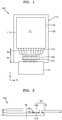
- FIG. 1 is a plan view of a display apparatus 100 according to an embodiment
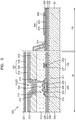
- FIG. 2 is a cross-sectional view of the display apparatus 100 of FIG. 1 .
- the display apparatus 100 includes a display panel 110.
- the display apparatus 100 may be an organic light-emitting display device (OLED).
- the display apparatus 100 may be a liquid crystal display (LCD), a field emission display (FED), or an electrophoretic display (EPD).
- the display panel 110 may include a display substrate 120 including a plurality of elements, and a thin-film encapsulation (TFE) layer 130 arranged above the display substrate 120.
- TFE thin-film encapsulation
- a plurality of thin-film transistors and a plurality of light-emitting elements respectively connected to the plurality of thin-film transistors may be arranged above the display substrate 120.
- a functional film 140 such as a polarizing layer, a touchscreen, and a cover window, may be arranged above the TFE layer 130.
- the display panel 110 may have an active area (AA) 111 on which an image is displayed, and an inactive area (IAA) 112 surrounding the active area 111.
- AA active area
- IAA inactive area
- the TFE layer 130 may cover the active area 111.
- the inactive area 112 surrounds the active area 111.
- the inactive area 112 may have a bending area BA in which the display panel 110 may be bent and a pad area PA disposed outside of the bending area BA.
- the display panel 110 may be bendable along a bending line BL that is a reference line in the bending area BA.
- the pad area PA may be arranged at one edge of the display substrate 120.
- a plurality of pads 150 may be arranged in the pad area PA.
- the plurality of pads 150 may be spaced apart from one another in an X direction of the display substrate 120.
- the pads 150 may be connected to wirings 113 extending from the active area 111.
- a driver 160 may be electrically connected to the plurality of pads 150.
- the driver 160 may include a driving circuit and may be a chip on plastic (COP).
- the driver 160 includes a flexible printed circuit board (PCB) 170 in which circuit wirings are patterned, a driving integrated circuit (IC) 180 arranged above the display substrate 120, and a plurality of driving terminals 190 arranged under the driving IC 180.
- the flexible PCB 170 may be electrically connected to the driving IC 180.
- the flexible PCB 170 may be electrically connected to an external board (not illustrated).
- the driver 160 may be a chip on film (COF). According to another embodiment, the driver 160 may be a chip on glass (COG).
- COF chip on film
- COG chip on glass
- the plurality of pads 150 may be electrically connected to the plurality of driving terminals 190.
- the plurality of pads 150 may be directly electrically connected to the plurality of driving terminals 190.
- An adhesive 210 may be arranged between the plurality of pads 150 and the plurality of driving terminals 190.
- the adhesive 210 may provide an adhesive force between the plurality of pads 150 and the plurality of driving terminals 190.
- the adhesive 210 may be arranged around a region where the plurality of pads 150 are connected to the plurality of driving terminals 190.
- the adhesive 210 may flow toward the periphery of the region where the plurality of pads 150 are connected to the plurality of driving terminals 190. Accordingly, the adhesive 210 may not be present in the region where the plurality of pads 150 are directly connected to the plurality of driving terminals 190 through the adhesive 210. In other words, the connection areas and/or electrically conducting faces of the pads 150 and driving terminals 190 may be maintained without adhesive 210 thereon or therebetween.
- the display apparatus 100 having the above-described structure may electrically connect the pads 150 to the driving terminals 190 by using a pressure device such as a hot bar.
- a pressure device such as a hot bar.
- the plurality of pads 150 may be arranged on the same plane above the display substrate 120.
- each of the plurality of pads 150 includes at least one conductive layer.
- the plurality of pads 150 may be arranged on different lines above the display substrate 120.
- the plurality of pads 150 arranged on the different lines may be alternately arranged.
- the plurality of pads 150 may be in a zigzag arrangement.
- FIG. 3 is a cross-sectional view of a display panel 300 according to an embodiment
- FIG. 4 is a plan view of one pad of FIG. 3
- FIG. 5 is a cross-sectional view taken along line V-V of FIG. 4 .
- the display panel 300 includes a display substrate 301 and a TFE layer 317.
- the display panel 300 may be an OLED panel.
- the display panel 300 may have a display area DA arranged in an active area AA, and a pad area PA arranged in an inactive area IAA.
- a pad 400 may be arranged in the pad area PA.
- the display substrate 301 may be a flexible glass substrate, a flexible polymer substrate, a rigid glass substrate, or a rigid polymer substrate.
- the display substrate 301 may be transparent, semitransparent, or opaque.
- a barrier film 302 may be arranged above the display substrate 301.
- the barrier film 302 may cover the display substrate 301.
- the barrier film 302 may be an organic film or an inorganic film.
- the barrier film 302 may be a single film or a multi-layer film.
- At least one thin-film transistor TFT and at least one capacitor Cst may be arranged above the display area DA. According to an embodiment, the number of thin-film transistors TFT and the number of capacitors Cst are not limited.
- a semiconductor active layer 303 may be arranged above the barrier film 302.
- the semiconductor active layer 303 includes a source region 304 and a drain region 305 arranged by doping N-type impurity ions or P-type impurity ions.
- a channel region 306 into which impurities are not doped may be disposed between the source region 304 and the drain region 305.
- the semiconductor active layer 303 may be an organic semiconductor or an inorganic semiconductor such as an amorphous silicon, a polysilicon and an oxide semiconductor.
- a gate insulating film 307 may be arranged above the semiconductor active layer 303.
- the gate insulating film 307 may be an inorganic film.
- the gate insulating film 307 may be a single film or a multi-layer film.
- a gate electrode 308 may be arranged above the gate insulating film 307.
- the gate electrode 308 may include a conductive material having conductivity, for example, metal such as molybdenum (Mo), aluminum (Al), copper (Cu) and titanium (Ti).
- the gate electrode 308 may be a single film or a multi-layer film.
- An interlayer insulating film 309 may be arranged above the gate electrode 308.
- the interlayer insulating film 309 may be an organic film or an inorganic film.
- a source electrode 310 and a drain electrode 311 may be arranged above the interlayer insulating film 309. Contact holes may be formed by removing portions of the gate insulating film 307 and portions of the interlayer insulating film 309.
- the source electrode 310 may be electrically connected to the source region through one of the contact holes
- the drain electrode 311 may be electrically connected to the drain region 305 through one of the contact holes.
- the source electrode 310 and the drain electrode 311 may include a conductive material having conductivity.
- the source electrode 310 and the drain electrode 311 includes metal such as Mo, Al, Cu and Ti.
- the source electrode 310 and the drain electrode 311 may be a single film or a multi-layer film.
- the source electrode 310 and the drain electrode 311 may have a stack structure including Ti/Al/Ti.
- a protective film 312 may be arranged above the source electrode 310 and the drain electrode 311.
- the protective film 312 may be an organic film or an inorganic film.
- the protective film 312 may include a passivation film and a planarization film. Either of the passivation film and the planarization film may be omitted.
- the capacitor Cst includes a first capacitor electrode CE1, a second capacitor electrode CE2, and a dielectric layer arranged therebetween.
- the dielectric layer may correspond to the interlayer insulating film 309.
- the first capacitor electrode CE1 may include the same material as the gate electrode 308 and may be arranged on the same plane as the gate electrode 308.
- the second capacitor electrode CE2 may include the same material as the source electrode 310 and the drain electrode 311 and may be arranged on the same plane as the source electrode 310 and the drain electrode 311.
- the protective film 312 may cover the second capacitor electrode CE2.
- the capacitor Cst may overlap the thin-film transistor TFT.
- the gate electrode 308 of the thin-film transistor TFT may function as the first capacitor electrode CE1.
- the second capacitor electrode CE2 may overlap the first capacitor electrode CE1, with the dielectric layer 1101 being arranged therebetween.
- the second capacitor electrode CE2 may include a conductive material having conductivity, for example, metal.
- the second capacitor electrode CE2 includes Mo, Al, Cu, or Ti.
- the second capacitor electrode CE2 may be a single film or a multi-layer film.
- the thin-film transistor TFT may be electrically connected to an OLED.
- the OLED may be arranged above the protective film 312.
- the OLED includes a first electrode 313, an intermediate layer 314, and a second electrode 315.
- the first electrode 313 may function as an anode and may include various conductive materials.
- the first electrode 313 may include a transparent electrode or a reflective electrode.
- the first electrode 313 includes a transparent conductive film.
- the first electrode 313 includes a reflective film and a transparent conductive film arranged above the reflective film.
- a pixel defining layer 316 may be arranged above the protective film 312.
- the pixel defining layer 316 may cover a portion of the first electrode 313.
- the pixel defining layer 316 surrounds an edge of the first electrode 313 to define an emission region of each sub-pixel.
- the first electrode 313 may be patterned in each sub-pixel.
- the pixel defining layer 316 may be an organic film or an inorganic film.
- the pixel defining layer 316 may be a single film or a multi-layer film.
- the intermediate layer 314 may be arranged above the first electrode 313 in a region corresponding to the first electrode 313 exposed by etching a part of the pixel defining layer 316.
- the intermediate layer 314 may be formed by a deposition process.
- the intermediate layer 314 may include an organic emissive layer.
- the intermediate layer 314 may include an organic emissive layer and may further include a hole injection layer (HIL), a hole transport layer (HTL), an electron transport layer (ETL), and an electron injection layer (EIL).
- HIL hole injection layer
- HTL hole transport layer
- ETL electron transport layer
- EIL electron injection layer
- the intermediate layer 314 may include an organic emissive layer and may further include various functional layers.
- the second electrode 315 may be arranged above the intermediate layer 314.
- the second electrode 315 may function as a cathode.
- the second electrode 315 may include a transparent electrode or a reflective electrode.
- the second electrode 315 when the second electrode 315 is the transparent electrode, the second electrode 315 includes a metal film and a transparent conductive film arranged above the metal film.
- the second electrode 315 when the second electrode 315 is the reflective electrode, the second electrode 315 includes a metal film.
- a plurality of sub-pixels may be arranged above the display substrate 301.
- a red color sub-pixel, a green color sub-pixel, a blue color sub-pixel, or a white color sub-pixel may be formed on the display substrate 301.
- the present disclosure is not limited thereto.
- the TFE layer 317 may cover the OLED.
- the TFE layer 317 may include first and second inorganic films 318 and 319 and an organic film 320 alternately stacked.
- the first inorganic film 318, the organic film 320, and the second inorganic film 319 may be sequentially stacked above the OLED.
- the stack structure of the inorganic films and the organic film included in the TFE layer 317 may be variously modified.
- a polarizing layer 321 may be arranged above the TFE layer 317.
- the polarizing layer 321 may reduce external light reflection.
- the polarizing layer 321 may be omitted, and external light reflection may be reduced by using a black matrix and a color filter.
- a plurality of pads 400 which are electrically connected to driving terminals, may be arranged in the pad area PA.
- Each pad 401 of the plurality of pads 400 may be spaced apart in one direction of the display substrate 301.
- Each pad 401 of the plurality of pads 400 may include a first conductive layer 410 and a second conductive layer 420 arranged above the first conductive layer 410.
- a first insulating film 331 may be arranged above the display substrate 301 in the pad area PA.
- the first insulating film 331 may be arranged on the same plane as the barrier film 302.
- the first insulating film 331 and the barrier film 302 may be formed in the same process by using the same material.
- a second insulating film 332 may be arranged above the first insulating film 331.
- the second insulating film 332 may be arranged on the same plane as the gate insulating film 307.
- the second insulating film 332 and the gate insulating film 307 may be formed in the same process by using the same material.
- the first conductive layer 410 included in each pad 401 may be arranged above the second insulating film 332.
- the first conductive layer 410 may be electrically connected to a wiring 322 extending from the gate electrode 308.
- the first conductive layer 410 may be arranged on the same plane as the gate electrode 308.
- the first conductive layer 410 and the gate electrode 308 may be formed in the same process by using the same material. Several first conductive layers 410 may be spaced apart from one another in one direction of the display substrate 301.
- a third insulating film 333 may be arranged above the first conductive layer 410.
- the third insulating film 333 may be arranged on the same plane as the interlayer insulating film 309.
- the third insulating film 333 and the interlayer insulating film 309 may be formed in the same process by using the same material.
- the third insulating film 333 may cover at least a portion of the first conductive layer 410.
- a plurality of contact holes 430 may be formed above the first conductive layer 410 by removing portions of the third insulating film 333. Top surfaces of the first conductive layers 410 may be exposed to the outside in a region where the contact holes 430 are formed.
- the contact holes 430 include a first contact hole 431 and a second contact hole 432 arranged adjacent to the first contact hole 431.
- the case where two contact holes 430 are arranged above the first conductive layer 410 has been described above, but embodiments are not limited as long as the number of contact holes 430 are two or more.
- a plurality of second conductive layers 420 may be arranged above the exposed region of the first conductive layer 410.
- the second conductive layer 420 may be electrically connected to the first conductive layer 410 through the contact hole 430.
- the plurality of second conductive layers 420 may be respectively arranged in the plurality of contact holes 430.
- one second conductive layer 420a may be arranged above the first contact hole 431, and another second conductive layer 420b may be arranged above the second contact hole 432.
- the plurality of second conductive layers 420a and 420b may be spaced apart from each other above the first conductive layer 410.
- the plurality of second conductive layers 420a and 420b may be connected to each other above the first conductive layer 410.
- the plurality of second conductive layers 420 may be arranged to have an island shape above the first conductive layer 410. According to another embodiment, the second conductive layer 420 may be electrically connected to a wiring extending from the display area DA.
- the second conductive layer 420 may be arranged on the same plane as the source electrode 310 and the drain electrode 311.
- the second conductive layer 420, the source electrode 310, and the drain electrode 311 may be formed in the same process by using the same material.
- the second conductive layer 420 may have a multi-layered structure. According to an embodiment, the second conductive layer 420 includes conductive portions of multiple layers.
- the second conductive layer 420 includes a first conductive portion 421, a second conductive portion 422, and a third conductive portion 423.
- the first conductive portion 421 may be arranged above the first conductive layer 410.
- the first conductive portion 421 includes Ti.
- the first conductive portion 421 may be directly connected to the first conductive layer 410.
- the second conductive portion 422 may be arranged above the first conductive portion 421.
- the second conductive portion 422 includes Al.
- the third conductive portion 423 may be arranged above the second conductive portion 422.
- the third conductive portion 423 includes Ti.
- the case where the second conductive layer 420 has the stack structure including Ti/Al/Ti has been described above, but the stack structure of the second conductive layer 420 may be variously modified.
- a clamping portion 424 which is connected to at least a portion of a driving terminal (640 of FIG. 6A ) of a driver, may be arranged between the adjacent second conductive layers 420a and 420b included in the second conductive layer 420.
- a clamping portion 424 may be formed on the third insulating film 333 to fully overlap with the third insulating film 333 in a plan view
- the clamping portion 424 includes an undercut 425 formed in the adjacent second conductive layers 420a and 420b.
- the undercut 425 may be provided by forming the first conductive portion 421, the second conductive portion 422, and the third conductive portion 423 to have different widths.
- the undercut 425 may be formed in the second conductive portion 422 where a width W2 of the second conductive portion 422 is narrower than a width W1 of the first conductive portion 421 and a width W3 of the third conductive portion 423 by from about 1 ⁇ m to about 20 ⁇ m.
- the width W1 of the first conductive portion 421 may be substantially equal to the width W3 of the third conductive portion 423.
- the second conductive layer 420 may be patterned by an etching process.
- an etch rate of the first conductive portion 421 and the third conductive portion 423 may be different from an etch rate of the second conductive portion 422.
- an etch rate of the second conductive portion 422 including Al may be larger than an etch rate of the first conductive portion 421 and the third conductive portion 423 each including Ti.
- the undercut 425 may be formed on opposite sidewalls of the adjacent second conductive layers 420a and 420b so that the second conductive portion 422 has a recessed portion.
- the driving terminal (640 of FIG. 6A ) of the driver may be strongly connected to the pad 401 having the above-described structure.
- FIG. 6A is a cross-sectional view illustrating a state before the driving terminal 640 is connected to the pad 401 of FIG. 5
- FIG. 6B is a cross-sectional view illustrating a state when the driving terminal 640 is connected to the pad 401 of FIG. 6A .
- a driving IC 610 may be arranged above the pad 401.
- a circuit pattern 620 may be arranged under the driving IC 610.
- An insulating film 630 may cover a portion of the circuit pattern 620.
- the driving terminal 640 may be electrically connected to the circuit pattern 620.
- the driving terminal 640 includes a bump 641.
- the bump 641 may include gold (Au), Cu, and indium (In).
- a solder layer 642 may be further arranged at the tip of the bump 641.
- the melting layer may be a solder layer 642.
- An adhesive 650 may be arranged between the pad 401 and the driving terminal 640.
- the adhesive 650 may be a non-conductive film (NCF).
- the adhesive 650 may not include a conductive material.
- the adhesive 650 may provide an adhesive force between the pad 401 and the driving terminal 640.
- the adhesive 650 may be arranged around a region where each pad 401 of the plurality of pads 400 is connected to each driving terminal 640 corresponding thereto.
- the attachment of the pad 401 and the bump 641 may be performed using a thermo-compression bonding process.
- a thermo-compression bonding process apparatus such as a hot bar
- the solder layer 642 provided in the bump 641 is melted so that the pad 401 is electrically connected (or bonded) to the driving terminal 640, as illustrated in FIG. 6B .
- delamination may occur between the pad 401 and the driving terminal 640 due to moisture absorption of the adhesive 650 arranged around a region where each pad 401 of the plurality of pad 400 is connected to the driving terminal 640 corresponding thereto.
- each pad 401 of the pads 400 may be tightly bonded to the driving terminal 640 corresponding thereto.
- the solder layer 642 provided in the bump 641 flows into the undercut 425 arranged on the opposite sidewalls of the adjacent second conductive layers 420a and 420b.
- the solder layer 642 may fill a gap between the adjacent second conductive layers 420a and 420b and may contact the opposite sidewalls of the adjacent second conductive layers 420a and 420b.
- the solder layer 642 provided on the bump 641 may extend over a region where the first conductive layer 410 contacts the second conductive layer 420 and between the adjacent second conductive layers 420a and 420b.
- the solder layer 642 provided on the bump 641 may completely cover the adjacent second conductive layers 420a and 420b.
- each pad 401 is in surface contact with the driving terminal 640 corresponding thereto through the solder layer 642 provided in the bump 641. Because the solder layer 642 fills the undercut between adjacent second conductive layer 420a and 420b, a contact resistance between the pad 401 and the driving terminal 640 may be reduced.
- the pad 401 may be strongly connected to the driving terminal 640.
- the pad 401 may be modified to have various shapes as long as the melting layer 642 provided in the bump 641 can fill the undercut between the conductive layers.
- FIG. 12 is a plan view of one pad according to an embodiment and FIG. 13 is a cross-sectional view taken along line XIII-XIII' of FIG. 12 .
- the second conductive layer 420 is formed in one piece and has a removed portion at the center.
- FIG. 14 is a plan view of one pad according to an embodiment and FIG. 15 is a cross-sectional view taken along line XV-XV' of FIG. 14 .
- a plurality of isolated second conductive layers 420 are arranged in a matrix configuration on the first conductive layer 410.
- FIG. 16 is a plan view of one pad according to an embodiment and FIG. 17 is a cross-sectional view taken along line XVII-XVII' of FIG. 16 .
- the second conductive layer 420 is formed as a mesh shape and has a plurality of removed portions arranged in a matrix shape on the first conductive layer 410.
- clamp portions connected to at least a part of the driving terminal 640 will be described.
- a clamping portion 724 which is connected to at least a portion of the driving terminal 640, may be arranged between adjacent second conductive layers 720a and 720b included in a second conductive layer 720.
- the clamping portion 724 includes an undercut 725 arranged on opposite sidewalls of the adjacent second conductive layers 720a and 720b.
- the first conductive layer 410 may be arranged on the same plane as the gate electrode 308 of FIG. 3 .
- the second conductive layer 720 may be arranged on the same plane as the source electrode 310 and the drain electrode 311 of FIG. 3 .
- the second conductive layer 720 may be a single film or a multi-layer film.
- the second conductive layer 720 includes a conductive portion of at least one layer.
- the undercut 725 may correspond to a region where the sidewall of the second conductive layer 720 is inclined.
- the second conductive layer 720 may have a reverse tapered shape.
- a clamping portion 824 may be arranged between adjacent second conductive layers 820a and 820b included in a second conductive layer 820.
- the clamping portion 824 includes an undercut 825 arranged on opposite sidewalls of the adjacent second conductive layers 820a and 820b.
- the second conductive layer 820 includes a conductive portion of at least one layer.
- the undercut 825 may correspond to a region where the sidewall of the second conductive layer 820 is curved.
- a clamping portion 924 may be arranged between adjacent second conductive layers 920a and 920b included in a second conductive layer 920.
- the clamping portion 924 includes an undercut 925 arranged on opposite sidewalls of the adjacent second conductive layers 920a and 920b.
- the second conductive layer 920 includes a conductive portion of at least one layer.
- the undercut 925 may correspond to a region where the sidewall of the second conductive layer 920 is curved.
- a third conductive layer 930 may be further arranged above the second conductive layer 920.
- the first conductive layer 410 may be arranged on the same plane as a gate electrode 308 of FIG. 11 .
- the second conductive layer 920 may be arranged on the same plane as a second capacitor electrode CE2 of FIG. 11 .
- the third conductive layer 930 may be arranged on the same plane as a source electrode 310 and a drain electrode 311 of FIG. 11 .
- the first to third conductive layers 410, 920, and 930 may be variously modified by combining a plurality of electrodes selected from among the gate electrode 308, the source electrode 310, the drain electrode 311, the capacitor electrodes CE1 and CE2, the first electrode 313, and the second electrode 315 of FIGS. 3 and 11 .
- a third conductive layer 1030 may be further arranged above a second conductive layer 1020.
- a clamping portion 1024 may be arranged between adjacent second conductive layers 1020a and 1020b included in the second conductive layer 1020.
- the clamping portion 1024 includes an undercut 1025 arranged on opposite sidewalls of the adjacent second conductive layers 1020a and 1020b.
- the second conductive layer 1020 includes a conductive portion of at least one layer.
- the undercut 1025 may correspond to a region where a width W2 of the second conductive layer 1020 is different from a width W3 of the third conductive layer 1030.
- the width W2 of the second conductive layer 1020 may be narrower than the width W3 of the third conductive layer 1030.
- the first conductive layer 1010 may be arranged on the same plane as the gate electrode 308 of FIG. 11 .
- the second conductive layer 1020 may be arranged on the same plane as the second capacitor electrode CE2 of FIG. 11 .
- the third conductive layer 1030 may be arranged on the same plane as the source electrode 310 and the drain electrode 311 of FIG. 11 .
- the first to third conductive layers 1010, 1020, and 1030 may be variously modified by combining a plurality of electrodes selected from the gate electrode 308, the source electrode 310, the drain electrode 311, the capacitor electrodes CE1 and CE2, the first electrode 313, and the second electrode 315 of FIGS. 3 and 11 .
- the display apparatus is capable of improving a connection force between the pad and the driving terminal. Therefore, it is possible to improve connection reliability between the pad and the driving terminal.
Landscapes
- Engineering & Computer Science (AREA)
- Microelectronics & Electronic Packaging (AREA)
- Physics & Mathematics (AREA)
- Geometry (AREA)
- Computer Hardware Design (AREA)
- General Physics & Mathematics (AREA)
- Theoretical Computer Science (AREA)
- Optics & Photonics (AREA)
- Manufacturing & Machinery (AREA)
- Devices For Indicating Variable Information By Combining Individual Elements (AREA)
- Electroluminescent Light Sources (AREA)
Abstract
Description
- One or more embodiments relate to a display apparatus.
- Display apparatuses may be used in mobile apparatuses such as smartphones, laptop computers, digital cameras, camcorders, portable information terminals, notebooks, and tablet personal computers (PCs), or electronic apparatuses such as desktop computers, televisions, outdoor billboards, and exhibition display apparatuses.
- Recently, slimmer display apparatuses have been launched.
- Flexible display apparatuses are easy to carry and are applicable to apparatuses having various shapes. Among them, a flexible display apparatus based on an organic light-emitting display technology is the most powerful flexible display apparatus.
- In the display apparatus, a pad on a display panel may be electrically connected to a pad of a driver. If the pad on the display panel and the pad of the driver are not reliably connected to each other, the reliability of the display apparatus may be deteriorated.
- One or more embodiments include a display apparatus in which a pad and a driving terminal are reliably connected to each other.
- Additional aspects will be set forth in part in the description which follows and, in part, will be apparent from the description, or may be learned by practice of the presented embodiments.
- According to one or more embodiments, a display apparatus includes: a display substrate; and a plurality of pads arranged above the display substrate, wherein each of the plurality of pads includes: a first conductive layer, at least a portion of which is covered by an insulating film; at least a second conductive layer arranged above the first conductive layer; and a clamping portion formed in the at least one second conductive layer. The clamping portion advantageously is adapted to receive a electrically conducting material of a driving terminal. Especially, the electrically conducting material electrically connects the first and/or second conductive layers via the driving terminal with a circuit pattern and/or a driving IC for driving the display apparatus. The electrically conducting material may be a melting or solder material melted and/or cast into the clamping portion for electrically connecting the driving terminal with the first and/or second conductive layers.
- The second conductive layer may include a plurality of second conductive layers which may be spaced apart from one another above the first conductive layer. This means, that there may be arranged a plurality of second conductive layers arranged over the first conductive layer, whereby a pluraility of second conductive layers may be provided in each of the plurality of pads.
- The insulating film may include a plurality of contact holes exposing top surfaces of the first conductive layer, and the plurality of second conductive layers may be electrically connected to the first conductive layer through the contact holes.
- The clamping portion may include an undercut arranged on opposite sidewalls of adjacent second conductive layers.
- The second conductive layer may include conductive portions of multiple layers, and the undercut may be provided by forming the conductive portions of multiple layers to have different widths.
- The second conductive layer may include: a first conductive portion connected to the first conductive layer; a second conductive portion arranged above the first conductive portion; and a third conductive portion arranged above the second conductive portion, and the undercut corresponds to a region where a width of the second conductive portion may be narrower than a width of the first conductive portion and a width of the third conductive portion.
- The second conductive layer may include a conductive portion of at least one layer, and the undercut may correspond to a region where a sidewall of the second conductive layer is inclined.
- The second conductive layer may include a conductive portion of at least one layer, and the undercut may correspond to a region where a sidewall of the second conductive layer is curved.
- The display apparatus may further include a third conductive layer arranged above the second conductive layer.
- The second conductive layer may include a conductive portion of at least one layer, the display apparatus may further include a third conductive layer arranged above the second conductive layer, and a width of the second conductive layer in the undercut may be narrower than a width of the third conductive layer.
- The display panel may include: at least one thin-film transistor including a semiconductor active layer, a gate electrode, a source electrode, and a drain electrode above the display substrate; an organic light-emitting display device electrically connected to the thin-film transistor, the organic light-emitting display device including a first electrode, an emission layer, and a second electrode; and an insulating film of at least one layer arranged between the thin-film transistor and the organic light-emitting display device, and the first conductive layer may be connected to a wiring extending from any one of the gate electrode, the source electrode, the drain electrode, the first electrode, and the second electrode, and the second conductive layer may be arranged to have an island shape above the first conductive layer.
- The first conductive layer may be formed of a same material as the gate electrode, and the second conductive layer may be formed of a same material as the source electrode and the drain electrode.
- The display apparatus may further include a third conductive layer disposed on the second conductive layer, wherein the first to third conductive layers may be a combination of a plurality of electrodes selected from the gate electrode, the source electrode, the drain electrode, the capacitor electrodes, the first electrode, and the second electrode.
- According to one or more embodiments, a display apparatus includes: a display panel including a display substrate in which a plurality of pads are arranged, and a thin-film encapsulation layer arranged above the display substrate; a driver including a plurality of driving terminals electrically connected to the plurality of pads; and an adhesive arranged between the plurality of pads and the driver, wherein each of the plurality of pads includes: a first conductive layer, at least a portion of which is covered by an insulating film; a plurality of second conductive layers arranged above the first conductive layer; and a clamping portion arranged between adjacent second conductive layers.
- The insulating film may include a plurality of contact holes exposing top surfaces of the first conductive layers, and the second conductive layers may be electrically connected to the first conductive layers through the contact holes, respectively.
- The clamping portion may include an undercut arranged on opposite sidewalls of the adjacent second conductive layers.
- The driving terminal may fill a gap between the adjacent second conductive layers and contact a sidewall of the second conductive layer in which the undercut is arranged.
- The driving terminal may extend over a region where the first conductive layer contacts the second conductive layer and between the adjacent second conductive layers.
- The each of the plurality of pads may be in surface contact with the driving terminal. The adhesive may include a non-conductive film.
- According to one or more embodiments, a display apparatus includes: a display panel comprising a display substrate in which a plurality of pads are arranged; and a driver comprising a plurality of driving terminals electrically connected to the plurality of pads, respectively, wherein each of the plurality of pads comprises: a first conductive layer; an insulating layer disposed on the first conductive layer, and a second conductive layer disposed on the insulating layer and connected to the first conductive layer through a contact hole formed in the insulating layer, and wherein the second conductive layer includes a clamping portion having an undercut and one of the plurality of driving terminals fills the undercut.
- The second conductive layer may include a first conductive portion and a second conductive portion disposed on the first conductive portion, and the undercut may be formed in the first conductive portion.
- The undercut may have a recessed portion recessed from an edge of the second conductive portion and the recessed portion may be from about 1 µm to about 20 µm.
- The clamping portion may be formed at a center of the second conductive layer.
- The second conductive layer may include a plurality of second conductive layers disposed on the first conductive layer, and the clamping portion may be formed between adjacent second conductive layers.
- These and/or other aspects will become apparent and more readily appreciated from the following description of the embodiments, taken in conjunction with the accompanying drawings in which:
-
FIG. 1 is plan view of a display apparatus according to an embodiment; -
FIG. 2 is a cross-sectional view of the display apparatus ofFIG. 1 ; -
FIG. 3 is a cross-sectional view of a display panel according to an embodiment; -
FIG. 4 is a plan view of a pad on a display pad ofFIG. 3 ; -
FIG. 5 is a cross-sectional view taken along line V-V ofFIG. 4 ; -
FIG. 6A is a cross-sectional view illustrating a state before a driving terminal is connected to a pad on a display panel ofFIG. 5 ; -
FIG. 6B is a cross-sectional view illustrating a state when a driving terminal is connected to a pad ofFIG. 6A ; -
FIGS. 7 to 10 are cross-sectional views illustrating states when a driving terminal is connected to a pad on a display panel, according to embodiments; and -
FIG. 11 is a cross-sectional view of one sub-pixel of a display panel, according to another embodiment. -
FIG. 12 is a plan view of one pad according to an embodiment. -
FIG. 13 is a cross-sectional view taken along line XIII-XIII' ofFIG. 12 . -
FIG. 14 is a plan view of one pad according to an embodiment. -
FIG. 15 is a cross-sectional view taken along line XV-XV' ofFIG. 14 . -
FIG. 16 is a plan view of one pad according to an embodiment. -
FIG. 17 is a cross-sectional view taken along line XVII-XVII' ofFIG. 16 . - Reference will now be made in detail to embodiments, examples of which are illustrated in the accompanying drawings, wherein like reference numerals refer to like elements throughout. In this regard, the present embodiments may have different forms and should not be construed as being limited to the descriptions set forth herein. Accordingly, the embodiments are merely described below, by referring to the figures, to explain aspects of the present description.
- Various alterations and modifications may be made to embodiments, some of which will be illustrated in detail in the drawings and detailed description. However, it should be understood that these embodiments are not construed as limited to the illustrated forms and include all changes, equivalents, or alternatives within the idea and the technical scope of the inventive concept. However, in the following descriptions and the accompanying drawings, descriptions of well-known functions and constructions will be omitted if they are considered to unnecessarily obscure the gist of the inventive concept.
- It will be understood that although the terms "first", "second", etc. may be used herein to describe various components, these components should not be limited by these terms. These components are only used to distinguish one component from another.
- The terminology used herein is for the purpose of describing particular embodiments only and is not intended to limit the scope of the inventive concept. As used herein, the singular forms "a", "an", and "the" are intended to include the plural forms as well, unless the context clearly indicates otherwise. It will be understood that the terms "comprise", "include", and "have" used herein specify the presence of stated features, integers, steps, operations, elements, components, or combinations thereof, but do not preclude the presence or addition of one or more other features, integers, steps, operations, elements, components, or combinations thereof.
- Hereinafter, a display apparatus according to one or more embodiments will be described in detail with reference to the accompanying drawings. Like reference numerals are assigned to like elements throughout the drawings and the specification, and redundant descriptions thereof will be omitted.
-
FIG. 1 is a plan view of adisplay apparatus 100 according to an embodiment, andFIG. 2 is a cross-sectional view of thedisplay apparatus 100 ofFIG. 1 . - Referring to
FIGS. 1 and 2 , thedisplay apparatus 100 includes adisplay panel 110. According to an embodiment, thedisplay apparatus 100 may be an organic light-emitting display device (OLED). According to another embodiment, thedisplay apparatus 100 may be a liquid crystal display (LCD), a field emission display (FED), or an electrophoretic display (EPD). - The
display panel 110 may include adisplay substrate 120 including a plurality of elements, and a thin-film encapsulation (TFE)layer 130 arranged above thedisplay substrate 120. A plurality of thin-film transistors and a plurality of light-emitting elements respectively connected to the plurality of thin-film transistors may be arranged above thedisplay substrate 120. Afunctional film 140, such as a polarizing layer, a touchscreen, and a cover window, may be arranged above theTFE layer 130. - The
display panel 110 may have an active area (AA) 111 on which an image is displayed, and an inactive area (IAA) 112 surrounding theactive area 111. - The
TFE layer 130 may cover theactive area 111. - The
inactive area 112 surrounds theactive area 111. Theinactive area 112 may have a bending area BA in which thedisplay panel 110 may be bent and a pad area PA disposed outside of the bending area BA. - The
display panel 110 may be bendable along a bending line BL that is a reference line in the bending area BA. - The pad area PA may be arranged at one edge of the
display substrate 120. A plurality ofpads 150 may be arranged in the pad area PA. The plurality ofpads 150 may be spaced apart from one another in an X direction of thedisplay substrate 120. Thepads 150 may be connected to wirings 113 extending from theactive area 111. - A
driver 160 may be electrically connected to the plurality ofpads 150. - The
driver 160 may include a driving circuit and may be a chip on plastic (COP). Thedriver 160 includes a flexible printed circuit board (PCB) 170 in which circuit wirings are patterned, a driving integrated circuit (IC) 180 arranged above thedisplay substrate 120, and a plurality of drivingterminals 190 arranged under the drivingIC 180. Theflexible PCB 170 may be electrically connected to the drivingIC 180. Theflexible PCB 170 may be electrically connected to an external board (not illustrated). - According to another embodiment, the
driver 160 may be a chip on film (COF). According to another embodiment, thedriver 160 may be a chip on glass (COG). - The plurality of
pads 150 may be electrically connected to the plurality of drivingterminals 190. The plurality ofpads 150 may be directly electrically connected to the plurality of drivingterminals 190. - An adhesive 210 may be arranged between the plurality of
pads 150 and the plurality of drivingterminals 190. The adhesive 210 may provide an adhesive force between the plurality ofpads 150 and the plurality of drivingterminals 190. The adhesive 210 may be arranged around a region where the plurality ofpads 150 are connected to the plurality of drivingterminals 190. - Specifically, when the plurality of
pads 150 are connected to the plurality of drivingterminals 190, the adhesive 210 may flow toward the periphery of the region where the plurality ofpads 150 are connected to the plurality of drivingterminals 190. Accordingly, the adhesive 210 may not be present in the region where the plurality ofpads 150 are directly connected to the plurality of drivingterminals 190 through the adhesive 210. In other words, the connection areas and/or electrically conducting faces of thepads 150 and drivingterminals 190 may be maintained without adhesive 210 thereon or therebetween. - The
display apparatus 100 having the above-described structure may electrically connect thepads 150 to the drivingterminals 190 by using a pressure device such as a hot bar. The case where thepads 150 above thedisplay substrate 120 are connected to the drivingterminals 190 of thedriver 160 has been described above, the present embodiment may be applied to any structure in which terminals arranged in different components are directly connected to one another. - According to an embodiment, the plurality of
pads 150 may be arranged on the same plane above thedisplay substrate 120. - According to an embodiment, each of the plurality of
pads 150 includes at least one conductive layer. - According to an embodiment, the plurality of
pads 150 may be arranged on different lines above thedisplay substrate 120. - According to an embodiment, the plurality of
pads 150 arranged on the different lines may be alternately arranged. For example, the plurality ofpads 150 may be in a zigzag arrangement. -
FIG. 3 is a cross-sectional view of adisplay panel 300 according to an embodiment,FIG. 4 is a plan view of one pad ofFIG. 3 , andFIG. 5 is a cross-sectional view taken along line V-V ofFIG. 4 . - Referring to
FIGS. 3 to 5 , thedisplay panel 300 includes adisplay substrate 301 and aTFE layer 317. According to an embodiment, thedisplay panel 300 may be an OLED panel. - The
display panel 300 may have a display area DA arranged in an active area AA, and a pad area PA arranged in an inactive area IAA. Apad 400 may be arranged in the pad area PA. - The
display substrate 301 may be a flexible glass substrate, a flexible polymer substrate, a rigid glass substrate, or a rigid polymer substrate. Thedisplay substrate 301 may be transparent, semitransparent, or opaque. - A
barrier film 302 may be arranged above thedisplay substrate 301. Thebarrier film 302 may cover thedisplay substrate 301. Thebarrier film 302 may be an organic film or an inorganic film. Thebarrier film 302 may be a single film or a multi-layer film. - At least one thin-film transistor TFT and at least one capacitor Cst may be arranged above the display area DA. According to an embodiment, the number of thin-film transistors TFT and the number of capacitors Cst are not limited.
- A semiconductor
active layer 303 may be arranged above thebarrier film 302. The semiconductoractive layer 303 includes asource region 304 and adrain region 305 arranged by doping N-type impurity ions or P-type impurity ions. Achannel region 306 into which impurities are not doped may be disposed between thesource region 304 and thedrain region 305. The semiconductoractive layer 303 may be an organic semiconductor or an inorganic semiconductor such as an amorphous silicon, a polysilicon and an oxide semiconductor. - A
gate insulating film 307 may be arranged above the semiconductoractive layer 303. Thegate insulating film 307 may be an inorganic film. Thegate insulating film 307 may be a single film or a multi-layer film. - A
gate electrode 308 may be arranged above thegate insulating film 307. Thegate electrode 308 may include a conductive material having conductivity, for example, metal such as molybdenum (Mo), aluminum (Al), copper (Cu) and titanium (Ti). Thegate electrode 308 may be a single film or a multi-layer film. - An interlayer insulating
film 309 may be arranged above thegate electrode 308. Theinterlayer insulating film 309 may be an organic film or an inorganic film. - A
source electrode 310 and adrain electrode 311 may be arranged above theinterlayer insulating film 309. Contact holes may be formed by removing portions of thegate insulating film 307 and portions of theinterlayer insulating film 309. Thesource electrode 310 may be electrically connected to the source region through one of the contact holes, and thedrain electrode 311 may be electrically connected to thedrain region 305 through one of the contact holes. - The
source electrode 310 and thedrain electrode 311 may include a conductive material having conductivity. For example, thesource electrode 310 and thedrain electrode 311 includes metal such as Mo, Al, Cu and Ti. Thesource electrode 310 and thedrain electrode 311 may be a single film or a multi-layer film. For example, thesource electrode 310 and thedrain electrode 311 may have a stack structure including Ti/Al/Ti. - A
protective film 312 may be arranged above thesource electrode 310 and thedrain electrode 311. Theprotective film 312 may be an organic film or an inorganic film. Theprotective film 312 may include a passivation film and a planarization film. Either of the passivation film and the planarization film may be omitted. - The capacitor Cst includes a first capacitor electrode CE1, a second capacitor electrode CE2, and a dielectric layer arranged therebetween. According to the present embodiment, the dielectric layer may correspond to the
interlayer insulating film 309. The first capacitor electrode CE1 may include the same material as thegate electrode 308 and may be arranged on the same plane as thegate electrode 308. The second capacitor electrode CE2 may include the same material as thesource electrode 310 and thedrain electrode 311 and may be arranged on the same plane as thesource electrode 310 and thedrain electrode 311. Theprotective film 312 may cover the second capacitor electrode CE2. - According to another embodiment, the capacitor Cst may overlap the thin-film transistor TFT.
- For example, referring to
FIG. 11 , thegate electrode 308 of the thin-film transistor TFT may function as the first capacitor electrode CE1. The second capacitor electrode CE2 may overlap the first capacitor electrode CE1, with thedielectric layer 1101 being arranged therebetween. The second capacitor electrode CE2 may include a conductive material having conductivity, for example, metal. The second capacitor electrode CE2 includes Mo, Al, Cu, or Ti. The second capacitor electrode CE2 may be a single film or a multi-layer film. - Referring to
FIGS. 3 ,4 , and5 again, the thin-film transistor TFT may be electrically connected to an OLED. - The OLED may be arranged above the
protective film 312. The OLED includes afirst electrode 313, anintermediate layer 314, and asecond electrode 315. - The
first electrode 313 may function as an anode and may include various conductive materials. Thefirst electrode 313 may include a transparent electrode or a reflective electrode. For example, when thefirst electrode 313 is the transparent electrode, thefirst electrode 313 includes a transparent conductive film. When thefirst electrode 313 is the reflective electrode, thefirst electrode 313 includes a reflective film and a transparent conductive film arranged above the reflective film. - A
pixel defining layer 316 may be arranged above theprotective film 312. Thepixel defining layer 316 may cover a portion of thefirst electrode 313. Thepixel defining layer 316 surrounds an edge of thefirst electrode 313 to define an emission region of each sub-pixel. Thefirst electrode 313 may be patterned in each sub-pixel. Thepixel defining layer 316 may be an organic film or an inorganic film. Thepixel defining layer 316 may be a single film or a multi-layer film. - The
intermediate layer 314 may be arranged above thefirst electrode 313 in a region corresponding to thefirst electrode 313 exposed by etching a part of thepixel defining layer 316. Theintermediate layer 314 may be formed by a deposition process. - The
intermediate layer 314 may include an organic emissive layer. - According to alternative examples, the
intermediate layer 314 may include an organic emissive layer and may further include a hole injection layer (HIL), a hole transport layer (HTL), an electron transport layer (ETL), and an electron injection layer (EIL). - According to an embodiment, the
intermediate layer 314 may include an organic emissive layer and may further include various functional layers. - The
second electrode 315 may be arranged above theintermediate layer 314. - The
second electrode 315 may function as a cathode. Thesecond electrode 315 may include a transparent electrode or a reflective electrode. For example, when thesecond electrode 315 is the transparent electrode, thesecond electrode 315 includes a metal film and a transparent conductive film arranged above the metal film. When thesecond electrode 315 is the reflective electrode, thesecond electrode 315 includes a metal film. - According to an embodiment, a plurality of sub-pixels may be arranged above the
display substrate 301. For example, a red color sub-pixel, a green color sub-pixel, a blue color sub-pixel, or a white color sub-pixel may be formed on thedisplay substrate 301. However, the present disclosure is not limited thereto. - The
TFE layer 317 may cover the OLED. - The
TFE layer 317 may include first and secondinorganic films organic film 320 alternately stacked. For example, the firstinorganic film 318, theorganic film 320, and the secondinorganic film 319 may be sequentially stacked above the OLED. The stack structure of the inorganic films and the organic film included in theTFE layer 317 may be variously modified. - A
polarizing layer 321 may be arranged above theTFE layer 317. Thepolarizing layer 321 may reduce external light reflection. According to another embodiment, thepolarizing layer 321 may be omitted, and external light reflection may be reduced by using a black matrix and a color filter. - A plurality of
pads 400, which are electrically connected to driving terminals, may be arranged in the pad area PA. Eachpad 401 of the plurality ofpads 400 may be spaced apart in one direction of thedisplay substrate 301. - Each
pad 401 of the plurality ofpads 400 may include a firstconductive layer 410 and a secondconductive layer 420 arranged above the firstconductive layer 410. - Details thereof will be described below.
- A first insulating
film 331 may be arranged above thedisplay substrate 301 in the pad area PA. The firstinsulating film 331 may be arranged on the same plane as thebarrier film 302. The firstinsulating film 331 and thebarrier film 302 may be formed in the same process by using the same material. - A second
insulating film 332 may be arranged above the first insulatingfilm 331. The secondinsulating film 332 may be arranged on the same plane as thegate insulating film 307. The secondinsulating film 332 and thegate insulating film 307 may be formed in the same process by using the same material. - The first
conductive layer 410 included in eachpad 401 may be arranged above the secondinsulating film 332. The firstconductive layer 410 may be electrically connected to awiring 322 extending from thegate electrode 308. The firstconductive layer 410 may be arranged on the same plane as thegate electrode 308. The firstconductive layer 410 and thegate electrode 308 may be formed in the same process by using the same material. Several firstconductive layers 410 may be spaced apart from one another in one direction of thedisplay substrate 301. - A third
insulating film 333 may be arranged above the firstconductive layer 410. The thirdinsulating film 333 may be arranged on the same plane as theinterlayer insulating film 309. The thirdinsulating film 333 and theinterlayer insulating film 309 may be formed in the same process by using the same material. - The third
insulating film 333 may cover at least a portion of the firstconductive layer 410. A plurality of contact holes 430 may be formed above the firstconductive layer 410 by removing portions of the thirdinsulating film 333. Top surfaces of the firstconductive layers 410 may be exposed to the outside in a region where the contact holes 430 are formed. - The contact holes 430 include a
first contact hole 431 and asecond contact hole 432 arranged adjacent to thefirst contact hole 431. The case where twocontact holes 430 are arranged above the firstconductive layer 410 has been described above, but embodiments are not limited as long as the number of contact holes 430 are two or more. - A plurality of second
conductive layers 420 may be arranged above the exposed region of the firstconductive layer 410. The secondconductive layer 420 may be electrically connected to the firstconductive layer 410 through thecontact hole 430. - The plurality of second
conductive layers 420 may be respectively arranged in the plurality of contact holes 430. For example, one secondconductive layer 420a may be arranged above thefirst contact hole 431, and another secondconductive layer 420b may be arranged above thesecond contact hole 432. The plurality of secondconductive layers conductive layer 410. However, the plurality of secondconductive layers conductive layer 410. - The plurality of second
conductive layers 420 may be arranged to have an island shape above the firstconductive layer 410. According to another embodiment, the secondconductive layer 420 may be electrically connected to a wiring extending from the display area DA. - The second
conductive layer 420 may be arranged on the same plane as thesource electrode 310 and thedrain electrode 311. The secondconductive layer 420, thesource electrode 310, and thedrain electrode 311 may be formed in the same process by using the same material. - The second
conductive layer 420 may have a multi-layered structure. According to an embodiment, the secondconductive layer 420 includes conductive portions of multiple layers. The secondconductive layer 420 includes a firstconductive portion 421, a secondconductive portion 422, and a thirdconductive portion 423. - The first
conductive portion 421 may be arranged above the firstconductive layer 410. The firstconductive portion 421 includes Ti. The firstconductive portion 421 may be directly connected to the firstconductive layer 410. The secondconductive portion 422 may be arranged above the firstconductive portion 421. The secondconductive portion 422 includes Al. The thirdconductive portion 423 may be arranged above the secondconductive portion 422. The thirdconductive portion 423 includes Ti. The case where the secondconductive layer 420 has the stack structure including Ti/Al/Ti has been described above, but the stack structure of the secondconductive layer 420 may be variously modified. - A clamping
portion 424, which is connected to at least a portion of a driving terminal (640 ofFIG. 6A ) of a driver, may be arranged between the adjacent secondconductive layers conductive layer 420. A clampingportion 424 may be formed on the thirdinsulating film 333 to fully overlap with the thirdinsulating film 333 in a plan view The clampingportion 424 includes an undercut 425 formed in the adjacent secondconductive layers - The undercut 425 may be provided by forming the first
conductive portion 421, the secondconductive portion 422, and the thirdconductive portion 423 to have different widths. The undercut 425 may be formed in the secondconductive portion 422 where a width W2 of the secondconductive portion 422 is narrower than a width W1 of the firstconductive portion 421 and a width W3 of the thirdconductive portion 423 by from about 1 µm to about 20 µm. The width W1 of the firstconductive portion 421 may be substantially equal to the width W3 of the thirdconductive portion 423. - The second
conductive layer 420 may be patterned by an etching process. When the secondconductive layer 420 is etched, an etch rate of the firstconductive portion 421 and the thirdconductive portion 423 may be different from an etch rate of the secondconductive portion 422. For example, an etch rate of the secondconductive portion 422 including Al may be larger than an etch rate of the firstconductive portion 421 and the thirdconductive portion 423 each including Ti. Accordingly, the undercut 425 may be formed on opposite sidewalls of the adjacent secondconductive layers conductive portion 422 has a recessed portion. - The driving terminal (640 of
FIG. 6A ) of the driver may be strongly connected to thepad 401 having the above-described structure. -
FIG. 6A is a cross-sectional view illustrating a state before the drivingterminal 640 is connected to thepad 401 ofFIG. 5 , andFIG. 6B is a cross-sectional view illustrating a state when the drivingterminal 640 is connected to thepad 401 ofFIG. 6A . - Referring to
FIG. 6A , a drivingIC 610 may be arranged above thepad 401. Acircuit pattern 620 may be arranged under the drivingIC 610. An insulatingfilm 630 may cover a portion of thecircuit pattern 620. The drivingterminal 640 may be electrically connected to thecircuit pattern 620. The drivingterminal 640 includes abump 641. Thebump 641 may include gold (Au), Cu, and indium (In). Asolder layer 642 may be further arranged at the tip of thebump 641. According to an embodiment, the melting layer may be asolder layer 642. - An adhesive 650 may be arranged between the
pad 401 and the drivingterminal 640. The adhesive 650 may be a non-conductive film (NCF). The adhesive 650 may not include a conductive material. The adhesive 650 may provide an adhesive force between thepad 401 and the drivingterminal 640. The adhesive 650 may be arranged around a region where eachpad 401 of the plurality ofpads 400 is connected to each driving terminal 640 corresponding thereto. - The attachment of the
pad 401 and thebump 641 may be performed using a thermo-compression bonding process. When a certain heat and pressure are applied from above the drivingIC 610 by using a thermo-compression bonding process apparatus such as a hot bar, thesolder layer 642 provided in thebump 641 is melted so that thepad 401 is electrically connected (or bonded) to the drivingterminal 640, as illustrated inFIG. 6B . - After the bonding, delamination may occur between the
pad 401 and the drivingterminal 640 due to moisture absorption of the adhesive 650 arranged around a region where eachpad 401 of the plurality ofpad 400 is connected to the driving terminal 640 corresponding thereto. - According to the present embodiment, since the clamping
portion 424 including the undercut 425 is arranged on the opposite sidewalls of the adjacent secondconductive layers conductive layer 420, eachpad 401 of thepads 400 may be tightly bonded to the driving terminal 640 corresponding thereto. - During the bonding, the
solder layer 642 provided in thebump 641 flows into the undercut 425 arranged on the opposite sidewalls of the adjacent secondconductive layers solder layer 642 may fill a gap between the adjacent secondconductive layers conductive layers - According to an embodiment, the
solder layer 642 provided on thebump 641 may extend over a region where the firstconductive layer 410 contacts the secondconductive layer 420 and between the adjacent secondconductive layers - According to an embodiment, the
solder layer 642 provided on thebump 641 may completely cover the adjacent secondconductive layers - According to an embodiment, each
pad 401 is in surface contact with the driving terminal 640 corresponding thereto through thesolder layer 642 provided in thebump 641. Because thesolder layer 642 fills the undercut between adjacent secondconductive layer pad 401 and the drivingterminal 640 may be reduced. - Subsequently, if a curing process is performed, the
pad 401 may be strongly connected to the drivingterminal 640. - According to an embodiment, the
pad 401 may be modified to have various shapes as long as themelting layer 642 provided in thebump 641 can fill the undercut between the conductive layers. -
FIG. 12 is a plan view of one pad according to an embodiment andFIG. 13 is a cross-sectional view taken along line XIII-XIII' ofFIG. 12 . Referring toFIGS. 12 and 13 , the secondconductive layer 420 is formed in one piece and has a removed portion at the center. -
FIG. 14 is a plan view of one pad according to an embodiment andFIG. 15 is a cross-sectional view taken along line XV-XV' ofFIG. 14 . Referring toFIGS. 14 and 15 , a plurality of isolated secondconductive layers 420 are arranged in a matrix configuration on the firstconductive layer 410. -
FIG. 16 is a plan view of one pad according to an embodiment andFIG. 17 is a cross-sectional view taken along line XVII-XVII' ofFIG. 16 . Referring toFIGS. 16 and 17 , the secondconductive layer 420 is formed as a mesh shape and has a plurality of removed portions arranged in a matrix shape on the firstconductive layer 410. - Hereinafter, clamp portions connected to at least a part of the driving
terminal 640, according to various embodiments, will be described. - Referring to
FIG. 7 , a clampingportion 724, which is connected to at least a portion of the drivingterminal 640, may be arranged between adjacent secondconductive layers conductive layer 720. The clampingportion 724 includes an undercut 725 arranged on opposite sidewalls of the adjacent secondconductive layers conductive layer 410 may be arranged on the same plane as thegate electrode 308 ofFIG. 3 . The secondconductive layer 720 may be arranged on the same plane as thesource electrode 310 and thedrain electrode 311 ofFIG. 3 . - The second
conductive layer 720 may be a single film or a multi-layer film. For example, the secondconductive layer 720 includes a conductive portion of at least one layer. The undercut 725 may correspond to a region where the sidewall of the secondconductive layer 720 is inclined. - According to an embodiment, the second
conductive layer 720 may have a reverse tapered shape. - Referring to
FIG. 8 , a clampingportion 824 may be arranged between adjacent secondconductive layers conductive layer 820. The clampingportion 824 includes an undercut 825 arranged on opposite sidewalls of the adjacent secondconductive layers - The second
conductive layer 820 includes a conductive portion of at least one layer. The undercut 825 may correspond to a region where the sidewall of the secondconductive layer 820 is curved. - Referring to
FIG. 9 , a clampingportion 924 may be arranged between adjacent secondconductive layers conductive layer 920. The clampingportion 924 includes an undercut 925 arranged on opposite sidewalls of the adjacent secondconductive layers - The second
conductive layer 920 includes a conductive portion of at least one layer. The undercut 925 may correspond to a region where the sidewall of the secondconductive layer 920 is curved. - Unlike in
FIG. 8A , a thirdconductive layer 930 may be further arranged above the secondconductive layer 920. The firstconductive layer 410 may be arranged on the same plane as agate electrode 308 ofFIG. 11 . The secondconductive layer 920 may be arranged on the same plane as a second capacitor electrode CE2 ofFIG. 11 . The thirdconductive layer 930 may be arranged on the same plane as asource electrode 310 and adrain electrode 311 ofFIG. 11 . - According to an embodiment, the first to third
conductive layers gate electrode 308, thesource electrode 310, thedrain electrode 311, the capacitor electrodes CE1 and CE2, thefirst electrode 313, and thesecond electrode 315 ofFIGS. 3 and11 . - Referring to
FIG. 10 , a thirdconductive layer 1030 may be further arranged above a secondconductive layer 1020. A clampingportion 1024 may be arranged between adjacent secondconductive layers conductive layer 1020. The clampingportion 1024 includes an undercut 1025 arranged on opposite sidewalls of the adjacent secondconductive layers - The second
conductive layer 1020 includes a conductive portion of at least one layer. The undercut 1025 may correspond to a region where a width W2 of the secondconductive layer 1020 is different from a width W3 of the thirdconductive layer 1030. The width W2 of the secondconductive layer 1020 may be narrower than the width W3 of the thirdconductive layer 1030. - The first
conductive layer 1010 may be arranged on the same plane as thegate electrode 308 ofFIG. 11 . The secondconductive layer 1020 may be arranged on the same plane as the second capacitor electrode CE2 ofFIG. 11 . The thirdconductive layer 1030 may be arranged on the same plane as thesource electrode 310 and thedrain electrode 311 ofFIG. 11 . - According to an embodiment, the first to third
conductive layers gate electrode 308, thesource electrode 310, thedrain electrode 311, the capacitor electrodes CE1 and CE2, thefirst electrode 313, and thesecond electrode 315 ofFIGS. 3 and11 . - As described above, the display apparatus according to one or more embodiments is capable of improving a connection force between the pad and the driving terminal. Therefore, it is possible to improve connection reliability between the pad and the driving terminal.
- It should be understood that embodiments described herein should be considered in a descriptive sense only and not for purposes of limitation. Descriptions of features or aspects within each embodiment should typically be considered as available for other similar features or aspects in other embodiments.
- While one or more embodiments have been described with reference to the figures, it will be understood by those of ordinary skill in the art that various changes in form and details may be made therein without departing from the scope as defined by the following claims.
Claims (13)
- A display apparatus comprising:a display substrate (301); anda plurality of pads (400, 401) arranged above the display substrate (301),wherein each of the plurality of pads (400, 401) comprises:a first conductive layer (410), at least a portion of which is covered by an insulating film (333);at least a second conductive layer (420, 720, 820, 920, 1020) arranged above the first conductive layer (410);characterized bya clamping portion (424, 724, 824, 924, 1024) formed in the at least one second conductive layer.
- The display apparatus of claim 1, wherein
a plurality of second conductive layers (420a, 420b, 720a, 720b, 820a, 820b, 920a, 920b, 1020a, 1020b) is provided, and
the second conductive layers (420a, 420b, 720a, 720b, 820a, 820b, 920a, 920b, 1020a, 1020b) are spaced apart from one another above the first conductive layer (410). - The display apparatus of claim 2, wherein
the insulating film (333) comprises a plurality of contact holes (430, 431, 432) exposing top surfaces of the first conductive layer (410), and
the plurality of second conductive layers (420a, 420b, 720a, 720b, 820a, 820b, 920a, 920b, 1020a, 1020b) are electrically connected to the first conductive layer (410) through the contact holes (430, 431, 432). - The display apparatus of claim 2 or 3, wherein
the clamping portion (424, 724, 824, 924, 1024) comprises an undercut (425, 725, 825, 925, 1025) arranged on opposite sidewalls of adjacent second conductive layers (420a, 420b, 720a, 720b, 820a, 820b, 920a, 920b, 1020a, 1020b). - The display apparatus of claim 4, wherein
the second conductive layer (420a, 420b, 920a, 920b, 1020a, 1020b) comprises conductive portions of multiple layers, and
the undercut (425, 925, 1025) is provided by forming the conductive portions of multiple layers to have different widths. - The display apparatus of claim 5, wherein
the second conductive layer (420, 420a, 420b) comprises:a first conductive portion (421) connected to the first conductive layer (410);a second conductive portion (422) arranged above the first conductive portion (421); anda third conductive portion (423) arranged above the second conductive portion (422), andthe undercut (425) corresponds to a region where a width (W2) of the second conductive portion (422) is narrower than a width (W1) of the first conductive portion (421) and a width (W3) of the third conductive portion (423). - The display apparatus of claim 4, wherein
the second conductive layer (720, 720a, 720b) comprises a conductive portion of at least one layer, and
the undercut (724) corresponds to a region where a sidewall of the second conductive layer (720, 720a, 720b) is inclined. - The display apparatus of claim 4, wherein
the second conductive layer (820, 920, 820a, 820b) comprises a conductive portion of at least one layer, and
the undercut (824, 924) corresponds to a region where a sidewall of the second conductive layer (820, 920, 820a, 820b) is curved. - The display apparatus of claim 8, further comprising:a third conductive layer (930) arranged above the second conductive layer (820, 920, 820a, 820b).
- The display apparatus of claim 4, wherein
the second conductive layer (1020, 1020a, 1020b) comprises a conductive portion of at least one layer,
the display apparatus further comprises a third conductive layer (1030) arranged above the second conductive layer (1020, 1020a, 1020b), and
a width (W2) of the second conductive layer (1020, 1020a, 1020b) in the undercut is narrower than a width (W3) of the third conductive layer (1030). - The display apparatus of at least one of claims 1 to 10, further comprising:a display panel (300) including:at least one thin-film transistor (TFT) comprising a semiconductor active layer (303), a gate electrode (308), a source electrode (310), and a drain electrode (311) above the display substrate (301);an organic light-emitting display device electrically connected to the thin-film transistor (TFT), the organic light-emitting display device comprising a first electrode (313), an emission layer, and a second electrode (315); andan insulating film (333) of at least one layer arranged between the thin-film transistor (TFT) and the organic light-emitting display device, andthe first conductive layer (410) is connected to a wiring extending from any one of the gate electrode (308), the source electrode (310), the drain electrode (311), the first electrode (313), and the second electrode (315), and the second conductive layer is arranged to have an island shape above the first conductive layer (410).
- The display apparatus of claim 11, wherein
the first conductive layer (410) is formed of a same material as the gate electrode (308), and
the second conductive layer (420, 720, 820, 920, 1020) is formed of a same material as the source electrode (310) and the drain electrode (311). - The display apparatus of claim 11 or 12, further comprising:a third conductive layer (930, 1030) arranged above the second conductive layer (920, 920a, 920b, 1020, 1020a, 1020b),wherein the first to third conductive layers (410, 920, 920a, 920b, 1020, 1020a, 1020b, 930, 1030) are a combination of a plurality of electrodes selected from the gate electrode (308), the source electrode (310), the drain electrode (311), the first electrode (313), and the second electrode (315).
Applications Claiming Priority (1)
| Application Number | Priority Date | Filing Date | Title |
|---|---|---|---|
| KR1020160079286A KR102663140B1 (en) | 2016-06-24 | 2016-06-24 | display device |
Publications (1)
| Publication Number | Publication Date |
|---|---|
| EP3261143A1 true EP3261143A1 (en) | 2017-12-27 |
Family
ID=59239790
Family Applications (1)
| Application Number | Title | Priority Date | Filing Date |
|---|---|---|---|
| EP17176787.4A Withdrawn EP3261143A1 (en) | 2016-06-24 | 2017-06-20 | Display apparatus |
Country Status (5)
| Country | Link |
|---|---|
| US (1) | US11171194B2 (en) |
| EP (1) | EP3261143A1 (en) |
| KR (1) | KR102663140B1 (en) |
| CN (1) | CN107546242B (en) |
| TW (1) | TWI747914B (en) |
Families Citing this family (9)
| Publication number | Priority date | Publication date | Assignee | Title |
|---|---|---|---|---|
| KR102591811B1 (en) * | 2018-05-18 | 2023-10-23 | 삼성디스플레이 주식회사 | Thin film transistor substrate, method of manufacturing the same, and display device including the same |
| KR102636629B1 (en) * | 2018-12-20 | 2024-02-13 | 엘지디스플레이 주식회사 | Display device |
| KR102769361B1 (en) * | 2019-04-01 | 2025-02-17 | 삼성디스플레이 주식회사 | Display device and method for manufacturing the same |
| CN112071819B (en) * | 2019-06-11 | 2023-05-16 | 群创光电股份有限公司 | electronic device |
| KR20200143563A (en) * | 2019-06-13 | 2020-12-24 | 삼성디스플레이 주식회사 | Display device |
| KR102844518B1 (en) * | 2019-12-24 | 2025-08-12 | 엘지디스플레이 주식회사 | Organic Light Emitting Display Apparatus |
| KR102909642B1 (en) * | 2020-02-20 | 2026-01-09 | 삼성디스플레이 주식회사 | Display device and method of manufacturing the same |
| KR20220007754A (en) * | 2020-07-09 | 2022-01-19 | 삼성디스플레이 주식회사 | Display device and tiled display device including the same |
| KR20220169981A (en) * | 2021-06-21 | 2022-12-29 | 삼성디스플레이 주식회사 | Display device and manufacturing method for the same |
Citations (6)
| Publication number | Priority date | Publication date | Assignee | Title |
|---|---|---|---|---|
| US5636329A (en) * | 1994-06-23 | 1997-06-03 | Nec Corporation | Liquid crystal display apparatus having terminal protected from break down |
| US5705855A (en) * | 1995-01-13 | 1998-01-06 | Motorola, Inc. | Integrated circuit for directly attaching to a glass substrate and method for manufacturing the same |
| US20070075313A1 (en) * | 2005-09-30 | 2007-04-05 | Won-Kyu Kwak | Flat panel display device |
| US20140327133A1 (en) * | 2013-05-06 | 2014-11-06 | Himax Technologies Limited | Metal bump structure for use in driver ic and method for forming the same |
| EP2966705A1 (en) * | 2014-07-11 | 2016-01-13 | LG Display Co., Ltd. | Organic light-emitting diode display device and method of fabricating the same |
| US20160070314A1 (en) * | 2014-09-05 | 2016-03-10 | Semiconductor Energy Laboratory Co., Ltd. | Display Panel, Input/output Device, and Data Processor |
Family Cites Families (23)
| Publication number | Priority date | Publication date | Assignee | Title |
|---|---|---|---|---|
| US5705885A (en) | 1994-11-25 | 1998-01-06 | Kabushiki Kaisha Toshiba | Brazing structure for X-ray image intensifier |
| JP3763607B2 (en) * | 1996-04-10 | 2006-04-05 | セイコーエプソン株式会社 | Method for manufacturing liquid crystal display device and liquid crystal display device |
| US5937320A (en) | 1998-04-08 | 1999-08-10 | International Business Machines Corporation | Barrier layers for electroplated SnPb eutectic solder joints |
| JP2000151057A (en) | 1998-11-09 | 2000-05-30 | Hitachi Ltd | Electronic component mounting structure, method of manufacturing the same, wireless IC card and method of manufacturing the same |
| JP2001109395A (en) | 1999-10-01 | 2001-04-20 | Sanyo Electric Co Ltd | EL display device |
| US6818545B2 (en) * | 2001-03-05 | 2004-11-16 | Megic Corporation | Low fabrication cost, fine pitch and high reliability solder bump |
| KR100790144B1 (en) | 2002-01-04 | 2007-12-31 | 삼성전자주식회사 | Solder Balls in Ball Grid Array Packages and Manufacturing Method for PC Pads |
| US6774026B1 (en) * | 2002-06-20 | 2004-08-10 | Taiwan Semiconductor Manufacturing Co., Ltd. | Structure and method for low-stress concentration solder bumps |
| JP2005070360A (en) | 2003-08-22 | 2005-03-17 | Sony Corp | Electric circuit board |
| JP2005109255A (en) | 2003-09-30 | 2005-04-21 | Optrex Corp | Terminal connection structure |
| KR20060134662A (en) | 2005-06-23 | 2006-12-28 | 엘지.필립스 엘시디 주식회사 | CIO type liquid crystal display device |
| JP2007041374A (en) * | 2005-08-04 | 2007-02-15 | Sharp Corp | Electrode substrate manufacturing method and liquid crystal display device manufacturing method |
| US8149346B2 (en) * | 2005-10-14 | 2012-04-03 | Semiconductor Energy Laboratory Co., Ltd. | Display device and manufacturing method thereof |
| KR101131230B1 (en) | 2009-05-06 | 2012-03-28 | 삼성전기주식회사 | A printed circuit board comprising a bump supporiting part and a method of manufacturing the same |
| KR101094292B1 (en) * | 2010-05-28 | 2011-12-19 | 삼성모바일디스플레이주식회사 | Organic light emitting display |
| US8647974B2 (en) | 2011-03-25 | 2014-02-11 | Ati Technologies Ulc | Method of fabricating a semiconductor chip with supportive terminal pad |
| KR20130013515A (en) * | 2011-07-28 | 2013-02-06 | 삼성디스플레이 주식회사 | Organic light emitting display apparatus |
| KR20140020565A (en) * | 2012-08-09 | 2014-02-19 | 삼성디스플레이 주식회사 | Organic light emitting display apparatus and method of manufacturing organic light emitting display apparatus |
| KR101444777B1 (en) * | 2012-08-10 | 2014-09-26 | 엘지디스플레이 주식회사 | Organic light emitting diode display device and method of fabricating the same |
| KR20150005105A (en) * | 2013-07-04 | 2015-01-14 | 삼성디스플레이 주식회사 | Display device |
| KR102145889B1 (en) * | 2013-12-20 | 2020-08-20 | 삼성디스플레이 주식회사 | Organic light emitting display apparatus and the manufacturing method thereof |
| CN103728763A (en) * | 2013-12-31 | 2014-04-16 | 深圳市华星光电技术有限公司 | LCD panel and manufacturing method thereof |
| KR102653947B1 (en) * | 2014-07-11 | 2024-04-03 | 엘지디스플레이 주식회사 | Display device and method of fabricating the same |
-
2016
- 2016-06-24 KR KR1020160079286A patent/KR102663140B1/en active Active
-
2017
- 2017-06-07 US US15/616,658 patent/US11171194B2/en active Active
- 2017-06-20 EP EP17176787.4A patent/EP3261143A1/en not_active Withdrawn
- 2017-06-23 TW TW106121061A patent/TWI747914B/en active
- 2017-06-26 CN CN201710493745.XA patent/CN107546242B/en active Active
Patent Citations (6)
| Publication number | Priority date | Publication date | Assignee | Title |
|---|---|---|---|---|
| US5636329A (en) * | 1994-06-23 | 1997-06-03 | Nec Corporation | Liquid crystal display apparatus having terminal protected from break down |
| US5705855A (en) * | 1995-01-13 | 1998-01-06 | Motorola, Inc. | Integrated circuit for directly attaching to a glass substrate and method for manufacturing the same |
| US20070075313A1 (en) * | 2005-09-30 | 2007-04-05 | Won-Kyu Kwak | Flat panel display device |
| US20140327133A1 (en) * | 2013-05-06 | 2014-11-06 | Himax Technologies Limited | Metal bump structure for use in driver ic and method for forming the same |
| EP2966705A1 (en) * | 2014-07-11 | 2016-01-13 | LG Display Co., Ltd. | Organic light-emitting diode display device and method of fabricating the same |
| US20160070314A1 (en) * | 2014-09-05 | 2016-03-10 | Semiconductor Energy Laboratory Co., Ltd. | Display Panel, Input/output Device, and Data Processor |
Also Published As
| Publication number | Publication date |
|---|---|
| TWI747914B (en) | 2021-12-01 |
| CN107546242B (en) | 2023-09-08 |
| US20170373028A1 (en) | 2017-12-28 |
| US11171194B2 (en) | 2021-11-09 |
| TW201810757A (en) | 2018-03-16 |
| CN107546242A (en) | 2018-01-05 |
| KR20180001640A (en) | 2018-01-05 |
| KR102663140B1 (en) | 2024-05-08 |
Similar Documents
| Publication | Publication Date | Title |
|---|---|---|
| US11997901B2 (en) | Display apparatus having grooved terminals | |
| US11171194B2 (en) | Display apparatus | |
| US10510821B2 (en) | Display device | |
| US10748853B2 (en) | Flexible display device | |
| US10230066B2 (en) | Organic light emitting display device having banks and method of manufacturing the same | |
| KR20130076399A (en) | Display device | |
| US9685494B2 (en) | Organic EL display device | |
| US9905631B2 (en) | Display device | |
| US12294044B2 (en) | Display device and method of manufacturing the same | |
| US20240121989A1 (en) | Display device and method of manufacturing the same | |
| KR102575480B1 (en) | display device | |
| US20240381698A1 (en) | Display device and method of manufacturing the same | |
| KR102878849B1 (en) | Display device |
Legal Events
| Date | Code | Title | Description |
|---|---|---|---|
| PUAI | Public reference made under article 153(3) epc to a published international application that has entered the european phase |
Free format text: ORIGINAL CODE: 0009012 |
|
| STAA | Information on the status of an ep patent application or granted ep patent |
Free format text: STATUS: THE APPLICATION HAS BEEN PUBLISHED |
|
| AK | Designated contracting states |
Kind code of ref document: A1 Designated state(s): AL AT BE BG CH CY CZ DE DK EE ES FI FR GB GR HR HU IE IS IT LI LT LU LV MC MK MT NL NO PL PT RO RS SE SI SK SM TR |
|
| AX | Request for extension of the european patent |
Extension state: BA ME |
|
| STAA | Information on the status of an ep patent application or granted ep patent |
Free format text: STATUS: REQUEST FOR EXAMINATION WAS MADE |
|
| 17P | Request for examination filed |
Effective date: 20180625 |
|
| RBV | Designated contracting states (corrected) |
Designated state(s): AL AT BE BG CH CY CZ DE DK EE ES FI FR GB GR HR HU IE IS IT LI LT LU LV MC MK MT NL NO PL PT RO RS SE SI SK SM TR |
|
| STAA | Information on the status of an ep patent application or granted ep patent |
Free format text: STATUS: THE APPLICATION IS DEEMED TO BE WITHDRAWN |
|
| 18D | Application deemed to be withdrawn |
Effective date: 20210112 |