EP3258503A1 - Mischgewebe zur elektrischen kontaktierung von photovoltaischen zellen - Google Patents
Mischgewebe zur elektrischen kontaktierung von photovoltaischen zellen Download PDFInfo
- Publication number
- EP3258503A1 EP3258503A1 EP16180461.2A EP16180461A EP3258503A1 EP 3258503 A1 EP3258503 A1 EP 3258503A1 EP 16180461 A EP16180461 A EP 16180461A EP 3258503 A1 EP3258503 A1 EP 3258503A1
- Authority
- EP
- European Patent Office
- Prior art keywords
- woven fabric
- conductive wires
- segment
- providing
- contact
- Prior art date
- Legal status (The legal status is an assumption and is not a legal conclusion. Google has not performed a legal analysis and makes no representation as to the accuracy of the status listed.)
- Granted
Links
Images


Classifications
-
- H—ELECTRICITY
- H10—SEMICONDUCTOR DEVICES; ELECTRIC SOLID-STATE DEVICES NOT OTHERWISE PROVIDED FOR
- H10F—INORGANIC SEMICONDUCTOR DEVICES SENSITIVE TO INFRARED RADIATION, LIGHT, ELECTROMAGNETIC RADIATION OF SHORTER WAVELENGTH OR CORPUSCULAR RADIATION
- H10F77/00—Constructional details of devices covered by this subclass
- H10F77/95—Circuit arrangements
- H10F77/953—Circuit arrangements for devices having potential barriers
- H10F77/955—Circuit arrangements for devices having potential barriers for photovoltaic devices
-
- H—ELECTRICITY
- H10—SEMICONDUCTOR DEVICES; ELECTRIC SOLID-STATE DEVICES NOT OTHERWISE PROVIDED FOR
- H10F—INORGANIC SEMICONDUCTOR DEVICES SENSITIVE TO INFRARED RADIATION, LIGHT, ELECTROMAGNETIC RADIATION OF SHORTER WAVELENGTH OR CORPUSCULAR RADIATION
- H10F19/00—Integrated devices, or assemblies of multiple devices, comprising at least one photovoltaic cell covered by group H10F10/00, e.g. photovoltaic modules
- H10F19/80—Encapsulations or containers for integrated devices, or assemblies of multiple devices, having photovoltaic cells
-
- H—ELECTRICITY
- H01—ELECTRIC ELEMENTS
- H01R—ELECTRICALLY-CONDUCTIVE CONNECTIONS; STRUCTURAL ASSOCIATIONS OF A PLURALITY OF MUTUALLY-INSULATED ELECTRICAL CONNECTING ELEMENTS; COUPLING DEVICES; CURRENT COLLECTORS
- H01R43/00—Apparatus or processes specially adapted for manufacturing, assembling, maintaining, or repairing of line connectors or current collectors or for joining electric conductors
- H01R43/02—Apparatus or processes specially adapted for manufacturing, assembling, maintaining, or repairing of line connectors or current collectors or for joining electric conductors for soldered or welded connections
- H01R43/0228—Apparatus or processes specially adapted for manufacturing, assembling, maintaining, or repairing of line connectors or current collectors or for joining electric conductors for soldered or welded connections without preliminary removing of insulation before soldering or welding
-
- H—ELECTRICITY
- H10—SEMICONDUCTOR DEVICES; ELECTRIC SOLID-STATE DEVICES NOT OTHERWISE PROVIDED FOR
- H10F—INORGANIC SEMICONDUCTOR DEVICES SENSITIVE TO INFRARED RADIATION, LIGHT, ELECTROMAGNETIC RADIATION OF SHORTER WAVELENGTH OR CORPUSCULAR RADIATION
- H10F19/00—Integrated devices, or assemblies of multiple devices, comprising at least one photovoltaic cell covered by group H10F10/00, e.g. photovoltaic modules
- H10F19/90—Structures for connecting between photovoltaic cells, e.g. interconnections or insulating spacers
- H10F19/902—Structures for connecting between photovoltaic cells, e.g. interconnections or insulating spacers for series or parallel connection of photovoltaic cells
- H10F19/904—Structures for connecting between photovoltaic cells, e.g. interconnections or insulating spacers for series or parallel connection of photovoltaic cells characterised by the shapes of the structures
-
- H—ELECTRICITY
- H10—SEMICONDUCTOR DEVICES; ELECTRIC SOLID-STATE DEVICES NOT OTHERWISE PROVIDED FOR
- H10F—INORGANIC SEMICONDUCTOR DEVICES SENSITIVE TO INFRARED RADIATION, LIGHT, ELECTROMAGNETIC RADIATION OF SHORTER WAVELENGTH OR CORPUSCULAR RADIATION
- H10F19/00—Integrated devices, or assemblies of multiple devices, comprising at least one photovoltaic cell covered by group H10F10/00, e.g. photovoltaic modules
- H10F19/90—Structures for connecting between photovoltaic cells, e.g. interconnections or insulating spacers
- H10F19/902—Structures for connecting between photovoltaic cells, e.g. interconnections or insulating spacers for series or parallel connection of photovoltaic cells
- H10F19/906—Structures for connecting between photovoltaic cells, e.g. interconnections or insulating spacers for series or parallel connection of photovoltaic cells characterised by the materials of the structures
-
- H—ELECTRICITY
- H10—SEMICONDUCTOR DEVICES; ELECTRIC SOLID-STATE DEVICES NOT OTHERWISE PROVIDED FOR
- H10F—INORGANIC SEMICONDUCTOR DEVICES SENSITIVE TO INFRARED RADIATION, LIGHT, ELECTROMAGNETIC RADIATION OF SHORTER WAVELENGTH OR CORPUSCULAR RADIATION
- H10F19/00—Integrated devices, or assemblies of multiple devices, comprising at least one photovoltaic cell covered by group H10F10/00, e.g. photovoltaic modules
- H10F19/90—Structures for connecting between photovoltaic cells, e.g. interconnections or insulating spacers
- H10F19/902—Structures for connecting between photovoltaic cells, e.g. interconnections or insulating spacers for series or parallel connection of photovoltaic cells
- H10F19/908—Structures for connecting between photovoltaic cells, e.g. interconnections or insulating spacers for series or parallel connection of photovoltaic cells for back-contact photovoltaic cells
-
- H—ELECTRICITY
- H10—SEMICONDUCTOR DEVICES; ELECTRIC SOLID-STATE DEVICES NOT OTHERWISE PROVIDED FOR
- H10F—INORGANIC SEMICONDUCTOR DEVICES SENSITIVE TO INFRARED RADIATION, LIGHT, ELECTROMAGNETIC RADIATION OF SHORTER WAVELENGTH OR CORPUSCULAR RADIATION
- H10F71/00—Manufacture or treatment of devices covered by this subclass
- H10F71/137—Batch treatment of the devices
- H10F71/1375—Apparatus for automatic interconnection of photovoltaic cells in a module
-
- H—ELECTRICITY
- H10—SEMICONDUCTOR DEVICES; ELECTRIC SOLID-STATE DEVICES NOT OTHERWISE PROVIDED FOR
- H10F—INORGANIC SEMICONDUCTOR DEVICES SENSITIVE TO INFRARED RADIATION, LIGHT, ELECTROMAGNETIC RADIATION OF SHORTER WAVELENGTH OR CORPUSCULAR RADIATION
- H10F77/00—Constructional details of devices covered by this subclass
- H10F77/20—Electrodes
- H10F77/206—Electrodes for devices having potential barriers
- H10F77/211—Electrodes for devices having potential barriers for photovoltaic cells
- H10F77/215—Geometries of grid contacts
-
- H—ELECTRICITY
- H10—SEMICONDUCTOR DEVICES; ELECTRIC SOLID-STATE DEVICES NOT OTHERWISE PROVIDED FOR
- H10F—INORGANIC SEMICONDUCTOR DEVICES SENSITIVE TO INFRARED RADIATION, LIGHT, ELECTROMAGNETIC RADIATION OF SHORTER WAVELENGTH OR CORPUSCULAR RADIATION
- H10F77/00—Constructional details of devices covered by this subclass
- H10F77/20—Electrodes
- H10F77/206—Electrodes for devices having potential barriers
- H10F77/211—Electrodes for devices having potential barriers for photovoltaic cells
- H10F77/219—Arrangements for electrodes of back-contact photovoltaic cells
-
- H—ELECTRICITY
- H01—ELECTRIC ELEMENTS
- H01R—ELECTRICALLY-CONDUCTIVE CONNECTIONS; STRUCTURAL ASSOCIATIONS OF A PLURALITY OF MUTUALLY-INSULATED ELECTRICAL CONNECTING ELEMENTS; COUPLING DEVICES; CURRENT COLLECTORS
- H01R4/00—Electrically-conductive connections between two or more conductive members in direct contact, i.e. touching one another; Means for effecting or maintaining such contact; Electrically-conductive connections having two or more spaced connecting locations for conductors and using contact members penetrating insulation
- H01R4/02—Soldered or welded connections
- H01R4/026—Soldered or welded connections comprising means for eliminating an insulative layer prior to soldering or welding
-
- Y—GENERAL TAGGING OF NEW TECHNOLOGICAL DEVELOPMENTS; GENERAL TAGGING OF CROSS-SECTIONAL TECHNOLOGIES SPANNING OVER SEVERAL SECTIONS OF THE IPC; TECHNICAL SUBJECTS COVERED BY FORMER USPC CROSS-REFERENCE ART COLLECTIONS [XRACs] AND DIGESTS
- Y02—TECHNOLOGIES OR APPLICATIONS FOR MITIGATION OR ADAPTATION AGAINST CLIMATE CHANGE
- Y02E—REDUCTION OF GREENHOUSE GAS [GHG] EMISSIONS, RELATED TO ENERGY GENERATION, TRANSMISSION OR DISTRIBUTION
- Y02E10/00—Energy generation through renewable energy sources
- Y02E10/50—Photovoltaic [PV] energy
Definitions
- the present invention relates to the field of photovoltaic cells, e.g. back-contact photovoltaic cells. More in particular, the present invention is related to methods for electrically contacting and encapsulating a back-contact photovoltaic cell, and to methods for interconnecting a plurality of back-contact photovoltaic cells in a photovoltaic module.
- back-contact photovoltaic cells e.g. silicon-based back-contact photovoltaic cells
- Such back-contact cells may advantageously achieve a good efficiency by avoiding the use of a conductive contact grid for current collection on the front surface of the cell.
- this potentially higher efficiency than typical for conventional front-contact cells may be explained by a lower self-shading due to absorption and/or reflection of incident radiation on the contact grid.
- Such efficiency gain may be particularly advantageous in high current cells, e.g. in concentrators or large area modules.
- a back-contact back-junction (BC-BJ) cell may have both negative and positive polarity current collection junctions located on the rear surface, e.g. the metallization and the contacted diffused regions may be located solely on the rear surface. Electron-hole pairs generated by light impinging on the front surface can be collected at the rear surface. Since such cells rely upon carrier collection at the rear surface alone, they may preferably have a particularly thin cell substrate of high quality material, e.g. a silicon material of high purity.
- interdigitated back contact (IBC) cells one such type of back-contact back-junction cell, emitter regions and back-surface field regions and the corresponding contacts of both polarities are provided on the rear surface of the cell, the respective contacts forming an interdigitated finger pattern.
- IBC interdigitated back contact
- EWT emitter wrap-through
- the metal wrap-through (MWT) cell In a similar type of back contact cell, the metal wrap-through (MWT) cell, a metal grid is wrapped from the front surface to the rear surface through a plurality of holes or vias through the substrate.
- This structure is akin to a conventional cell structure. While the emitter is provided on the front side, busbars are provided on the rear surface, leaving only a thin front surface grid on the illuminated surface that is connected to the rear surface by extending it through a number of metallised openings or vias in the wafer.
- back-contact cells regardless of the specific type, current is collected at contact points or contact areas on the rear surface, e.g. by soldering connectors to the contact busbars or pads.
- at least one connector may be soldered to a series of negative polarity contacts and at least one may be soldered to a series of positive polarity contacts.
- both polarities of a back-contact photovoltaic cell need to be contacted on the rear surface of the cell, e.g. in order to interconnect such back-contact cells in a module, additional electrical insulation may be required.
- conductors for connecting different polarities might need to cross each other, or a conductor may need to cross an area of a different polarity on the rear surface, such that an insulating layer may be required to avoid short circuiting.
- the required insulation may be achieved by incorporation of additional materials in the module, such as solder masks, glass fibre and/or polymers.
- solder masks such as solder masks, glass fibre and/or polymers.
- such means for providing the necessary insulation can adversely affect the cost and complexity of the module, and may even reduce the reliability.
- a hybrid Leno-woven material made of conductive wires interwoven with insulating wires for contacting and/or connecting back-contact photovoltaic cells.
- the wires are provided using a Leno weaving pattern, in which the conductive wires are used as filling threads in the weft direction and the insulating wires as warp threads, such that the conductive wires remain spatially separated by insulating threads from a cell surface when the material is applied against the surface.
- it is a disadvantage of such approach that separate interconnection and lamination steps may be required.
- conductors for connecting such cells are efficiently insulated to prevent short circuiting.
- photovoltaic cells e.g. back-contact photovoltaic cells
- photovoltaic cells may be electrically contacted and/or electrically interconnected, without dispensing pastes, e.g. solder and/or conductive paste, and therefore, costs, process steps, cell handling operations, and/or alignment steps related to paste dispensing can be avoided.
- dispensing pastes e.g. solder and/or conductive paste
- cell manipulation operations for connecting the cells can be limited to a single manipulation step for final placement during lay-up.
- contacts for connecting each of both polarities are provided on a single surface by conductive structures while simultaneously providing insulating, e.g. encapsulating, material.
- a single lay-up step may be required in accordance with embodiments of the present invention for forming electrical contacts for both polarities and for encapsulation, e.g. no separate alignment step is required for insulator and conductor.
- interconnection steps for soldering or curing can be avoided, e.g. by advantageously providing interconnections simultaneously during a lamination and encapsulation process.
- solder-coated ribbons can be directly soldered, when provided in a weave, onto cell contact busbars and/or cell contact pads.
- the contacting and insulating, e.g. encapsulating, structure provided by embodiments can compensate stresses, e.g. forms an out-of-plane stress relief structure.
- stresses generated during temperature variations and processing, and/or mechanical stresses on a photovoltaic module can be compensated, e.g. can be absorbed and dispersed efficiently.
- thermal expansion compensation structures may be provided by embodiments of the present invention, e.g. integrated in the woven fabric.
- a woven material can be provided for electrically contacting photovoltaic cells that has a simple weave and that can be manufactured and applied in large dimension formats.
- a woven material can be provided and used that may only contain encapsulant ribbons and conductive connection ribbons.
- end bussing of cell strings may not be required, e.g. an end bus can be provided in the weave during weaving, e.g. as integral part of the woven fabric.
- a back-contact back-junction photovoltaic cell e.g. an interdigitated back-contact cell
- a back-contact back-junction photovoltaic cell can be manufactured cheaply, e.g. a busbar or part of a busbar as provided in conventional IBC cells can be replaced by an electrically conductive ribbon integrated in a weave or woven fabric in accordance with embodiments.
- less metallization on cell level may be required, e.g. less silver metallization.
- a tapering structure can be provided in a woven fabric, allowing optimization of electrically conductive ribbon cross sections and resistive losses, e.g. to achieve a high fill factor relative to the total cross-section of conductors provided in the weave or woven fabric, and further simplifying the interconnection layout.
- the present invention relates to a method for contacting and electrically connecting at least one photovoltaic cell.
- the method comprises providing at least one photovoltaic cell, wherein said at least one photovoltaic cell comprises at least a first metal contact of a first polarity and a second metal contact of a second, opposite, polarity on a single surface thereof.
- the method comprises providing a woven fabric comprising a plurality of insulating ribbons, arranged in a single one of a warp direction and a weft direction of the woven fabric, and a plurality of conductive wires, arranged in at least a weft direction or a warp direction of the woven fabric, the plurality of conductive wires being provided at least in a direction different from the direction in which the plurality of insulating ribbons is arranged, wherein at least one of the plurality of conductive wires comprises at least a first segment and a second segment that are electrically isolated from each other.
- the method comprises bringing the woven fabric into physical contact with said surface of the at least one photovoltaic cell.
- the method comprises performing a heating process to establish an electrical connection between the first metal contact and the first segment and to establish an electrical connection between the second metal contact and the second segment, wherein this heating process furthermore liquefies the plurality of insulating ribbons to transform the insulating ribbons into an encapsulation layer.
- providing the woven fabric may comprise providing said woven fabric in the form of a twill weave fabric or a twill-like weave fabric.
- providing the woven fabric may comprise providing said woven fabric wherein said plurality of conductive wires comprise copper ribbons coated with a solder material.
- providing the woven fabric may comprise providing said woven fabric wherein said insulating ribbons are composed of a transparent material.
- providing the woven fabric may comprise weaving the plurality of insulating ribbons and a plurality of conductive wires.
- providing the woven fabric may further comprise slitting an insulating foil and/or a conductive foil to respectively form the plurality of insulating ribbons and/or the plurality of conductive wires.
- providing the woven fabric may further comprise providing holes in the woven fabric for locally interrupting the at least one of the plurality of conductive wires comprising at least a first segment and a second segment, to thereby electrically disconnect the at least one first segment and the at least one second segment.
- providing the at least one photovoltaic cell may comprise providing a plurality of back-contact photovoltaic cells.
- providing the at least one photovoltaic cell may comprise providing a plurality of emitter wrap-through photovoltaic cells and/or a plurality of metal wrap-through photovoltaic cells.
- providing the woven fabric may comprise providing the woven fabric comprising a first plurality of first conductive wires arranged in a single one of the a weft direction and the warp direction of the woven fabric, the direction in which the first plurality of first conductive wires is arranged being different from the direction in which the plurality of insulating ribbons is arranged.
- providing the woven fabric may comprise providing the woven fabric in which a plurality of first conductive wires are provided, e.g. woven, such that a weave pattern, e.g. a twill pattern, exposes each of said plurality of first conductive wires at a first predetermined location corresponding to a location of a first contact, and exposes each of said plurality of first conductive wires at a second predetermined location corresponding to a location of a second contact, wherein each of said plurality of first conductive wires is exposed at both the first predetermined location and the second predetermined location on a surface of the woven fabric for contacting the photovoltaic cell.
- a weave pattern e.g. a twill pattern
- providing the woven fabric may comprise providing the woven fabric in which each of said plurality of first conductive wires crosses over at least one insulating ribbon in between the first predetermined location and the second predetermined location to be exposed at a surface of the woven fabric opposite of the surface for contacting the photovoltaic cell.
- providing the woven fabric may comprise providing the woven fabric in which said first segment comprises the first predetermined location and said second segment comprises the second predetermined location, and wherein said first segment and said second segment are disconnected from each other by a hole interrupting the first conductive wire, the hole being provided where said first conductive wire crosses over the at least one insulating ribbon in between the first predetermined location and the second predetermined location to be exposed at a surface opposite of the surface for contacting the photovoltaic cell.
- providing said woven fabric may comprise providing the woven fabric wherein two string end busbars are interwoven at opposite ends of the first plurality of first conductive wires, each string end busbar comprising a further conductive wire arranged on, and oriented along, a corresponding insulating ribbon, such that electrical contacts are established between first segments and the first string end busbar and electrical contacts are established between second segments and the second string end busbar.
- providing the at least one photovoltaic cell may comprise providing a plurality of interdigitated back-contact photovoltaic cells.
- providing the woven fabric may comprise providing the woven fabric comprising a first plurality of first electrically conductive wires arranged in a direction of the woven fabric different from the direction in which the plurality of insulating ribbons is arranged and a second plurality of second conductive wires arranged in the direction of the woven fabric in which the plurality of insulating ribbons is arranged, wherein each of the second plurality of conductive wires is arranged on a corresponding insulating ribbon and oriented along a central longitudinal axis thereof.
- providing the woven fabric may comprise providing the woven fabric having a weave pattern, e.g. a twill weave fabric having a twill weave pattern, in which the first plurality of first conductive wires are double weft per pick such as to form aligned pairs of conductive wires of the first plurality of first conductive wires.
- a weave pattern e.g. a twill weave fabric having a twill weave pattern
- providing the woven fabric may comprise providing the woven fabric in which the first plurality of first conductive wires are provided, e.g. woven, such that a weave pattern, e.g. a twill weave pattern, exposes a conductive wire of a plurality of aligned pairs, e.g. of each aligned pair, at a first predetermined location corresponding to a location of a first contact, and exposes the other conductive wire of said plurality of aligned pairs, e.g. of each aligned pair, at a second predetermined location corresponding to a location of a second contact, wherein the conductive wires of said plurality of pairs, e.g. of each pair, are exposed at respectively the first predetermined location and the second predetermined location on a surface of the woven fabric for contacting the photovoltaic cell.
- a weave pattern e.g. a twill weave pattern
- providing the woven fabric may comprise providing the woven fabric in which said conductive wires of a pair cross over a same insulating ribbon and its corresponding conductive wire of the second plurality of second conductive wires such to form electrical connections between respectively a conductive wire of said pair and said first segment and said other conductive wire of said pair and said second segment, wherein the first segment and the second segment are segments of said corresponding conductive wire of the second plurality of second conductive wires.
- providing the woven fabric may comprise providing the woven fabric in which said first segment and said second segment are disconnected from each other by a hole interrupting said corresponding conductive wire of the second plurality of second conductive wires the hole being provided in between said conductive wire of said pair and said other conductive wire of said pair.
- providing the at least one photovoltaic cell may comprise providing a busbar-less interdigitated back-contact photovoltaic cell, wherein said first metal contact and said second metal contact correspond to opposite polarity regions of fingers formed on the busbar-less interdigitated back-contact photovoltaic cell.
- providing said busbar-less interdigitated back-contact photovoltaic cell may comprise providing said photovoltaic cell comprising local interconnections for forming interconnecting bridges between fingers corresponding to the same charge polarity over regions where the first plurality of first conductive wires of the woven fabric, when contacted to the photovoltaic cell, are woven such that the weave pattern, e.g. twill pattern, exposes first plurality of first conductive wires at the surface of the woven fabric opposite of the surface for contacting the photovoltaic cell.
- the weave pattern e.g. twill pattern
- the present invention relates to a woven fabric for use in a method according to embodiments of the first aspect of the present invention, the woven fabric comprising a plurality of insulating ribbons, arranged in a single one of a a warp direction and a weft direction of the woven fabric, and a plurality of conductive wires, arranged in at least a weft direction or a warp direction of the woven fabric, the plurality of conductive wires being arranged at least in a direction different from the direction in which the plurality of insulating ribbons is arranged wherein at least one of the plurality of conductive wires comprises at least a first segment and a second segment that are electrically isolated from each other.
- the present invention also relates to a photovoltaic module obtainable by interconnecting a plurality of photovoltaic cells in accordance with a method according to embodiments of the first aspect of the present invention.
- the front surface or front side of a photovoltaic cell or of a photovoltaic module is the surface or side adapted for being oriented towards a light source and thus for receiving illumination.
- both surfaces are adapted to receive impinging light.
- the front surface or front side is the surface or side adapted for receiving the largest fraction of the light or illumination.
- the back surface, rear surface, back side or rear side of a photovoltaic cell or a photovoltaic module is the surface or side opposite to the front surface or side.
- a busbar is an electrically conductive strip for collecting an electrical current, e.g. a current generated under illumination, from a plurality of metal contacts or metal electrodes provided on a surface of a photovoltaic cell.
- a busbar is provided for direct electrical connection with an external electrical lead.
- a busbar typically collects the electrical current from finer or narrower metal contacts, also called metal fingers, on the cell. These finer or narrower metal contacts collect an electrical current from the cell and deliver the current to the busbars; they are typically not provided for direct electrical connection to an external electrical lead.
- a busbar-free photovoltaic cell is a photovoltaic cell not having busbars.
- a busbar-free photovoltaic cell typically comprises a plurality of metal contacts or metal electrodes on a surface of the cell but after cell fabrication it does not comprise an electrically conductive element for collecting current from the plurality of metal contacts.
- electrically conductive elements such as for example electrically conductive wires are soldered to the plurality of metal contacts. These electrically conductive elements are provided for collecting an electrical current from the plurality of metal electrodes and they replace the conventional busbars.
- a twill fabric or a twill weave is a weave wherein one or more weft yarns (or warp yarns) alternately pass over and under two or more warp yarns (or weft yarns respectively) in a regular repeated manner, with a step or offset between rows.
- Twill weave is a basic weave characterized by pronounced diagonal ridges, called twill lines.
- the construction of a twill weave may be identified by a fraction, in which the numerator indicates the number of warp threads crossing over a number of weft threads as indicated in the denominator. For example, for an uneven 3/1 ratio twill, the warp wire may sequentially be crossing over three weft wires and under one weft wire.
- the present invention relates to a method for contacting at least one photovoltaic cell, e.g. electrically contacting at least one photovoltaic cell.
- the present invention further relates to a method for electrically interconnecting a plurality of photovoltaic cells, for example to form a photovoltaic module.
- the photovoltaic cell may comprise a back-contact photovoltaic cell, e.g. the plurality of photovoltaic cells may comprise a plurality of back-contact photovoltaic cells. It is an advantage of embodiments of the present invention that a substantially monolithic module-level integration of photovoltaic cells can be achieved using simple and cost-efficient techniques.
- the method comprises providing at least one photovoltaic cell.
- This at least one photovoltaic cell comprises at least one first metal contact of a first polarity and at least one second metal contact of a second polarity, opposite to the first polarity, on a surface of the cell, i.e. on the same surface, e.g. back surface, of the cell.
- the photovoltaic cell e.g. the plurality of photovoltaic cells, may for example comprise an emitter wrap-through (EWT) or metal wrap-through (MWT) back-contact photovoltaic cell.
- EWT emitter wrap-through
- MTT metal wrap-through
- the photovoltaic cell e.g.
- the plurality of photovoltaic cells may comprise a back-contact back-junction (BC-BJ) photovoltaic cell, e.g. an interdigitated back-contact (IBC) photovoltaic cell, the present invention not being limited thereto.
- BC-BJ back-contact back-junction
- IBC interdigitated back-contact
- the method comprises providing a woven fabric.
- the woven fabric may be a twill weave fabric, or a twill-like weave fabric, e.g. a fabric woven by a weaving technique derived from a twill weave, e.g. a combination twill weave or pointed twill weave, the present invention not being limited thereto.
- the woven fabric comprises a plurality of electrically insulating ribbons arranged in a single one of a warp direction and a weft direction of the woven fabric, and a plurality of electrically conductive wires arranged in at least a weft direction or a warp direction of the woven fabric, the plurality of electrically conductive wires being arranged in at least a direction different from the direction in which the plurality of insulating ribbons is arranged.
- the woven fabric may comprise a first plurality of first electrically conductive wires, the first plurality of first electrically conductive wires being arranged in a direction different from the direction in which the plurality of insulating ribbons is arranged, and such woven fabric may e.g. comprise no electrically conductive wires arranged in the direction in which the plurality of insulating ribbons is arranged.
- the woven fabric may comprise a first plurality of first electrically conductive wires, the first plurality of first electrically conductive wires being arranged in a direction different from the direction in which the plurality of insulating ribbons is arranged, and the woven fabric may further comprise a second plurality of second electrically conductive wires, the second plurality of second electrically conductive wires being arranged in a direction corresponding to the direction in which the plurality of insulating ribbons is arranged.
- the woven fabric comprises a plurality of electrically insulating ribbons arranged in a warp direction of the woven fabric, and a plurality of electrically conductive wires arranged in at least a weft direction of the woven fabric.
- the woven fabric may comprise a first plurality of first electrically conductive wires arranged in a weft direction, and the woven fabric may e.g. comprise no electrically conductive wires arranged in a warp direction.
- the woven fabric may comprise a first plurality of first electrically conductive wires arranged in a weft direction and the woven fabric may further comprise a second plurality of second electrically conductive wires arranged in a warp direction. It is an advantage of embodiments having the electrically insulating ribbons being arranged in a warp direction that it may allow easier or faster fabrication (weaving) of the woven fabric as compared to embodiments wherein the electrically insulating ribbons are arranged in a weft direction.
- the further description relates to embodiments wherein the electrically insulating ribbons are provided in a warp direction of the woven fabric.
- the present invention in not limited thereto and it also includes embodiments wherein the electrically insulating ribbons are provided in a weft direction of the woven fabric.
- the electrically conductive wires may comprise electrically conductive ribbons.
- the conductive wires, e.g. ribbons, may thus be secured in the woven fabric by weaving them with the electrically insulating ribbons.
- the electrically conductive wires may comprise a metal, e.g. a low resistance metal, such as copper, aluminum, gold or silver.
- the electrically conductive wires may comprise copper ribbons.
- the electrically conductive wires may be coated with a solderable material, e.g. a solder.
- the electrically conductive wires may comprise solder-coated copper ribbons.
- the conductive wires may be coated with a low temperature solder material, e.g. a solder alloy for soldering at a temperature in the range of 20°C and 300°C, e.g. in the range of 50°C and 150°C, e.g. in the range of 60°C and 100°C.
- a solder alloy comprising Ag, Bi, Sn, Pb, Cd, Zn or In may be used, the present invention not being limited thereto.
- the electrically insulating ribbons may be made of a polymer, e.g. a polymer suitable for photovoltaic encapsulation purposes.
- the insulating ribbons may be composed of a thermoplastic polymer and/or of a polymer that allows ensuring sufficient structural and electrical separation and insulation between the electrically conductive wires before, during and after lamination.
- the insulating ribbons may comprise a polyolefin encapsulant material, or an EVA (ethylene vinyl acetate) encapsulant material or a multi-layer material such as for example an EVA/polyolefin/EVA stack, the present invention not being limited thereto.
- the electrically insulating ribbons may be transparent, or may be adapted for transforming into a transparent material by liquefaction and subsequent solidification into the encapsulation layer referred to further hereinbelow.
- transparency may be advantageous for use in double glass building-integrated photovoltaic modules, e.g. with large spacing between cells, to allow sufficient light to pass through the module for indoor lighting purposes and/or for a substantially unobstructed view through the module.
- the electrically insulating ribbons may be coloured, e.g. to hide the conducting wires between the cells, for example for aesthetical reasons.
- the electrically insulating ribbons may furthermore be relatively wide, e.g. wider than the second electrically conductive ribbons or wires, which are arranged in the same direction as the electrically insulating ribbons, such as for example more in particular in the warp direction.
- the electrically insulating ribbons may be e.g. at least twice as wide, e.g.
- At least thrice as wide for example at least five times as wide, as compared to the second electrically conductive ribbons or wires, such as to allow a good lateral insulation of adjacent electrically conductive wires in the weft direction and to allow - where required - a good insulation in a direction orthogonal to the plane of the woven fabric between a first electrically conductive ribbon arranged in the weft direction and a crossing second electrically conductive ribbon arranged in the warp direction.
- an intentional electrical connection or an intentional electrical contact can be provided between electrically conductive wires, e.g. between a first electrically conductive wire and a crossing second electrically conductive wire, as will be described further hereinbelow.
- the insulating ribbons e.g. insulating polymer ribbons
- a width of 7.5 mm could correspond to about 20 insulating ribbons to cover a cell of about 15 cm.
- the second electrically conductive wires may for example comprise a conductive ribbon of 1 mm width, e.g. in the range of 500 ⁇ m to 5 mm, e.g.
- the first electrically conductive wires may for example have a width in the same range or in the same order as the second electrically conductive wires or they may have a different width, e.g. a larger width.
- the electrically conductive ribbons may for example have a height or thickness in the range of 10 ⁇ m to 200 ⁇ m, e.g. in the range of 40 ⁇ m to 120 ⁇ m, e.g. 70 ⁇ m, the present invention not being limited thereto.
- the electrically insulating ribbons may for example have a height or thickness the range between 100 ⁇ m to 1 mm, e.g. in the range between 200 ⁇ m and 600 ⁇ m, such as e.g. in the order of 400 ⁇ m, the present invention not being limited thereto.
- providing the woven fabric may comprise a step of weaving the plurality of insulating ribbons and the plurality of electrically conductive wires.
- the woven fabric may be obtained as a pre-woven fabric.
- the electrically insulating ribbons and/or the electrically conductive ribbons may for example be obtained by slitting respectively an insulating foil, e.g. an encapsulant foil, and a conductive foil, e.g. a metal foil, such as a copper foil. Then, the slits or slitted parts of the insulating foil (the insulating ribbons) and the slits or slitted parts of the conductive foil (the conductive ribbons) may be woven to form the woven fabric.
- an insulating foil e.g. an encapsulant foil
- a conductive foil e.g. a metal foil, such as a copper foil.
- a heating step may be performed, for example comprising heating to a temperature lower than the melting temperature of the electrically insulating ribbons, such as for example to a temperature in the range between 90°C and 110°C, at which the electrically insulating material becomes sticky.
- Such heating step may advantageously result in a fixation of the electrically insulating ribbons and the electrically conductive ribbons within the fabric.
- providing the woven fabric may comprise slitting an insulating foil and/or a conductive foil to respectively form the plurality of insulating ribbons and/or the plurality of conductive wires (in the form of conductive ribbons).
- the weaving pattern of the insulating ribbons and conductive wires may expose the first electrically conductive wires arranged in the weft direction to both sides of the woven fabric, i.e. at some locations the first electrically conductive wires may be exposed at a first side of the woven fabric and at other locations the first electrically conductive wires may be exposed at a second, opposite, side of the woven fabric.
- at least part of the first electrically conductive wires arranged in the weft direction that is exposed at a side for contacting the photovoltaic cell may be electrically connectable to contact pads or busbars of the photovoltaic cell, e.g. by soldering.
- first electrically conductive wires may replace the busbars or cell string interconnections, e.g. they may have the function of a busbar or of a string interconnection.
- contact side or “first side of the woven fabric” will refer to the side of the woven fabric that is intended to be directly contacted to the photovoltaic cell in accordance with a method of embodiments of the present invention
- non-contact side or “second side of the woven fabric” will refer to the opposite side that is not intended to be directly contacted to the photovoltaic cell in a method in accordance with embodiments of the present invention.
- this naming convention should not be construed as implying any other properties of or differences between these opposite sides of the woven fabric.
- the "contact side” may equally refer to the a side of the woven fabric at a moment in time where no contact is not yet established with this side, and the "non-contact side” is nonetheless contactable by arbitrary means, yet not intended to directly and physically contact the photovoltaic cell in accordance with embodiments of the present invention.
- At least one of the plurality of electrically conductive wires comprises, e.g. is divided into, at least a first segment and a second segment that are electrically insulated from each other, e.g. to electrically isolate two distinct end regions of the wire in the warp or weft direction.
- providing the woven fabric may comprise providing holes in the woven fabric for locally severing or separating the at least one first segment and the at least one second segment.
- at least one of, for example a plurality of, e.g. each one of, the first electrically conductive wires may comprise, e.g.
- the woven fabric may be divided into, at least a first segment and a second segment that are electrically insulated from each other.
- the woven fabric comprises second electrically conductive ribbons arranged in the warp direction
- at least one of, for example a plurality of, e.g. each one of, the second electrically conductive wires may comprise, e.g. may be divided into, at least a first segment and a second segment that are electrically insulated from each other.
- a hole may be provided to locally sever or interrupt at least one of the plurality of electrically conductive wires.
- Such hole may, for example, be provided in a part of the electrically conductive wire that is exposed at a surface of the woven fabric opposite of the surface that will be used for contacting the photovoltaic cell, as described further hereinbelow, the present invention not being limited thereto.
- the hole may also penetrate the insulating ribbon where the conductive wire is supported by the insulating ribbon.
- the diameter, e.g. a width and/or height, of the hole may be less than the width of the insulating ribbon, yet at least as wide as the conductive wire.
- the method further comprises bringing the woven fabric into physical contact with a surface of the at least one photovoltaic cell where the electrical contacts of the cell are located, e.g. with corresponding surface sides of the plurality of photovoltaic cells, e.g. with the back surface of the at least one photovoltaic cell.
- the at least one photovoltaic cell comprises, on this surface for contacting the woven fabric, at least one first metal contact of a first polarity and at least one second metal contact of a second polarity opposite to the first polarity.
- the method also comprises performing a heating process for establishing an electrical connection between a first metal contact and a first electrically conductive wire oriented in the weft direction to form a conductive path between the first metal contact and a first segment, and to establish an electrical connection between a second metal contact and a first electrically conductive wire oriented in the weft direction to form a conductive path between the second metal contact and a second segment.
- the first segment and the second segment may thus be adapted for collecting a current from the first and second metal contacts respectively by the electrical connections formed in this step of performing a heating process.
- this heating process is also adapted for liquefying, e.g. melting, the plurality of insulating ribbons, e.g. polymer ribbons, to transform these insulating ribbons into an encapsulation layer.
- a uniform ribbon and encapsulant composite may be created, while keeping the conductive wires separated or contacted as intended by the structure of the weave.
- a layer of encapsulation material may be formed on the backside of the back-contact cells that is sufficient for the cell encapsulation, i.e. such that there is no need for providing additional encapsulation material or an additional encapsulation layer at the back side of the cells when performing a cell encapsulation process.
- a connection soldering step of the conductive wires, e.g. conductive ribbons, to the contacts of the cell, and of crossing contacting ribbons in the weave, can thus be advantageously combined with an encapsulation step.
- the method in accordance with embodiments may also comprise contacting at least one conductive wire, e.g. the first segment and/or the second segment, e.g. on a part thereof that is exposed on the side that is opposite of the side contacting the cell, by at least one module terminal to form an electrical connection. Since the conducting wires are contactable on both sides of the woven fabric, connection of module terminals can be done during the encapsulation process.
- the photovoltaic cell e.g. the plurality of photovoltaic cells, may comprise a back-contact back-junction (BC-BJ) photovoltaic cell, e.g. an interdigitated back-contact (IBC) photovoltaic cell.
- BC-BJ back-contact back-junction
- IBC interdigitated back-contact
- the first segment and the second segment may be electrically connected to the first and the second metal contact respectively such as to collect a current from the back side of the BC-BJ photovoltaic cell, e.g. from IBC cell busbars or contact pads.
- the method may furthermore comprise aligning the at least one photovoltaic cell and the woven fabric, e.g. prior to bringing the woven fabric into contact with the photovoltaic cell, such as to align the second metal contact with the second segment and the first metal contact with the first segment.
- the present invention also relates to a woven fabric for use in a method in accordance with embodiments of the first aspect of the present invention.
- embodiments of the present invention may relate to a woven fabric 10, 60 for use in a method according to embodiments of the first aspect of the present invention.
- the woven fabric comprises a plurality of insulating ribbons, arranged in a warp direction of the woven fabric, and a plurality of conductive wires, arranged in at least a weft direction of the woven fabric, wherein at least one of the plurality of conductive wires comprises at least a first segment and a second segment that are electrically isolated from each other.
- the present invention is not limited thereto and in other embodiments of the present invention the woven fabric may comprise a plurality of insulating ribbons arranged in a weft direction of the woven fabric and a plurality of conductive wires arranged in at least a warp direction of the woven fabric, wherein at least one of the plurality of conductive wires comprises at least a first segment and a second segment that are electrically isolated from each other.
- the present invention also relates to a photovoltaic module obtainable by interconnecting a plurality of photovoltaic cells in accordance with a method according to embodiments of the first aspect of the present invention.
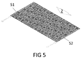
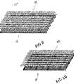
- FIG 1 illustrates a first exemplary woven fabric 10 in accordance with embodiments of the present invention, e.g. for use in a method in accordance with embodiments of the present invention.
- the woven fabric 10 illustrated in FIG 1 comprises a plurality of electrically insulating ribbons 11 in a warp direction and a plurality of first electrically conductive ribbons 12 in a weft direction.
- it may comprise electrically conductive string end-busbars being provided in the warp direction.
- the first electrically conductive ribbons 12 are interrupted at predetermined locations, e.g. by stamping, punching or cutting a hole 15, such that the first electrically conductive ribbons 12 comprise, e.g. are divided into, at least a first segment 13 and a second segment 14 that are electrically insulated from each other.
- This woven fabric 10 may form, after application of the heating process in accordance with a method of embodiments of the present invention, an encapsulant sheet with integrated interconnections, for use in contacting and electrically connecting photovoltaic cells, e.g. BC cells. More in particular, this exemplary woven fabric 10 may be used for electrically contacting and electrically connecting, e.g. interconnecting, back-contact cells such as metal wrap-through or emitted wrap-through cells, e.g. a back-contact cell in which no busbar metallization is provided nor required on the back surface of the photovoltaic cell.
- back-contact cells such as metal wrap-through or emitted wrap-through cells
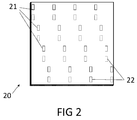
- FIG 2 illustrates, schematically, a back surface of such an exemplary back-contact photovoltaic cell 20, e.g. a metal wrap-through cell, for use in combination with an exemplary woven fabric 10 in accordance with embodiments of the present invention as shown in FIG 1 .
- the photovoltaic cell 20 comprises, on the surface for contacting the woven fabric, e.g. on the rear surface opposite of the front surface for being oriented to a source of illumination in operation of the cell, at least one first metal contact 21 and at least one second metal contact 22 of opposite polarity with respect to the first metal contact.
- a plurality of first contacts 21 may consist of contact pads operably connected via wrap-through connections to a frontside grid of the cell, e.g. for providing emitter contacts to the cell
- the plurality of second contacts 22 may consist of contact pads to regions of opposite polarity at the backside of the cell, e.g. for providing base contacts or back surface field contacts to the cell.
- the exemplary woven fabric 10 in accordance with embodiments of the present invention, comprises a plurality of electrically insulating ribbons 11 arranged in a warp direction 2 of the woven fabric.
- the woven fabric 10 also comprises a plurality of first electrically conductive wires 12, arranged in the weft direction 3 of the woven fabric.
- the woven fabric 10 may be a twill or twill-like weave fabric, e.g. a combination twill or a pointed twill weave pattern.
- This twill or twill-like pattern may advantageously implement a tapering design, as will be described hereinbelow.
- the plurality of first conductive wires 12 may be woven such that the weave pattern, e.g. a twill pattern, exposes the conductive wire at a surface for contacting the photovoltaic cell at a first predetermined location 16 corresponding to a location of a first contact 21 of the photovoltaic cell 20, and for exposing the conductive wire at this surface for contacting at a second predetermined location 17 corresponding to a location of a second contact 22 of the photovoltaic cell 20.
- the weave pattern e.g. a twill pattern
- the conductive wire 12 crosses over at least one insulating ribbon 11 to be exposed at the non-contact side in between the first predetermined location 16 and the second predetermined location 17.
- the conductive wire 12 crosses over at least one insulating ribbon 11 to be exposed at the non-contact side in between the first predetermined location 16 and the second predetermined location 17.
- two picks of the conductive wires 12 are provided on the contact side of the fabric 10 and all other picks of the conductive wires are provided on the non-contact side.
- one pick is provided on the non-contact side in between the first predetermined location 16 and the second predetermined location 17.
- the weave configuration e.g. the twill ratio or twill combination configuration, may be selected based on the layout of the contacts to be contacted on the photovoltaic cell 20, as will be readily understood to the skilled person.
- At least one of the plurality of first electrically conductive wires 12 comprises at least a first segment 13 and a second segment 14 that are electrically insulated from each other, e.g. by a hole 15 separating the first segment 13 from the second segment 14.
- the first conductive wires 12 may be severed or interrupted by a corresponding hole 15 provided through the conductive wire 12 and the insulating ribbon 11 directly underneath.
- Such hole may be provided by stamping or locally cutting the conductive wire 12, e.g. stamping or cutting the conductive wire and the overlapping part of the insulating ribbon.
- the width of the hole 15 may be smaller than the width of the insulating ribbon, e.g. such as to maintain a structural integrity provided by the warp oriented ribbon.
- the first segment 13 may comprise the first predetermined location 16, and the second segment 14 may comprise the second predetermined location 17.
- a hole 15, or a different type of electrical interruption for at least electrically disconnecting the first segment from the second segment may be provided in between the contact-side first predetermined location 16 and the contact-side second predetermined location 17, e.g. in at least one pick of the conductive wire 12 on the non-contact side of the fabric 10.
- the electrical interruptions may be provided in each conductive wire 12 at a fixed position with respect to the twill-like weave pattern, e.g. at a fixed pick in the pick sequence. Due to a fixed offset of the weave pattern, e.g. the pick pattern, in one conductive wire with respect to a next wire, the electrical interruptions may form a tapered structure in the woven fabric.
- each wire may provide a segment for contacting a negative polarity contact of the photovoltaic cell at one end and a segment for contacting a positive polarity contact of the photovoltaic cell at the other end.
- a method in accordance with embodiments of the present invention may comprise aligning the at least one photovoltaic cell 20 and the woven fabric 10, e.g. prior to bringing the woven fabric into contact with the photovoltaic cell, such as to align the first predetermined location 16 with a location of a first contact 21 on the photovoltaic cell 20, and to align the second predetermined location 17 with a location of a second contact 22.
- first segments 13 of the first electrically conductive wires 12 may be electrically connected to the photovoltaic cells to carry a first charge polarity, e.g. connected to '-' terminals, and second segments 14 of the first electrically conductive wires 12 may be electrically connected to the photovoltaic cells to carry a second charge polarity opposite to the first charge polarity, e.g. connected to '+' terminals.
- string end-busbars may be interwoven at the end of a cell string.
- the first segments 13 of the conductive wires that are electrically connected to the photovoltaic cells to carry a first charge polarity, e.g. connected to '-' terminals may electrically contact a first string end busbar 51, e.g. provided on the 'non-contact' side of an insulating ribbon 11, i.e. on the side of the insulating ribbon that is facing away from the photovoltaic cell.
- the first segments 13 of the conductive wires 12 are woven such as to be exposed at the 'non-contact' side of the fabric 10, thus enabling contacting the first string end busbar 51.
- the second segments 14 of the conductive wires that are electrically connected to the photovoltaic cells to carry a second charge polarity opposite to the first charge polarity may electrically contact a second string end busbar 52, in the same manner as discussed hereinabove for the first segments 13 in relation to the first string end busbar 51.
- These string end busbars 51, 52 may extend or connect to similar busbars of adjacent cells.
- adjacent to the woven fabric 10, in the warp direction 2 another similar or identical woven fabric 10 connected to photovoltaic cells 20 may be provided.
- the cells in the neighbouring string may be rotated 180°, such as to reverse the polarities of the string end busbars at corresponding ends of the adjacent fabrics. This enables a connection of positive to negative terminals of adjacent cell strings via extension and/or interconnection of the string end busbars 51, 52, e.g. such as to form a series interconnection between cell strings.
- the photovoltaic cell or a plurality of photovoltaic cells may be provided on, e.g. laid on, a transparent front carrier 42 such as a glass plate, with a front side of the photovoltaic cells being oriented towards the front carrier 42, afterwards the woven fabric 10 may be provided on, e.g. laid on, the photovoltaic cells and aligned with the photovoltaic cells, and a back carrier 41, e.g. a further glass plate or backsheet, may be provided on, e.g. laid on, the woven fabric, in view of forming an encapsulated photovoltaic module.
- a transparent front carrier 42 such as a glass plate
- an encapsulant e.g. a transparent encapsulant
- the material of the insulating ribbons may function as an encapsulant.
- the amount of encapsulation material provided by the insulating ribbons 11 may be sufficient, i.e. there may be no need for providing additional encapsulation material or an additional encapsulation layer.
- a heating process is performed, thereby transforming the material of the electrically insulating ribbons into an encapsulant layer, e.g. by liquefying the insulating ribbons.
- the photovoltaic cells 20 are electrically connected and physically bonded to the woven fabric 10.
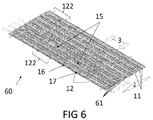
- FIG 6 illustrates a second exemplary woven fabric 60 in accordance with embodiments of the present invention, e.g. for use in a method in accordance with embodiments of the present invention.
- This woven fabric 60 may form, after application of the heating process in accordance with a method of embodiments of the present invention, an encapsulant sheet with integrated interconnections, for use in contacting and electrically connecting photovoltaic cells, e.g. back-contact back-junction (BC-BJ) cells. More in particular, this exemplary woven fabric 60 may be used for electrically contacting and electrically connecting, e.g. interconnecting, interdigitated back-contact (IBC) cells, e.g.
- IBC interdigitated back-contact
- the second exemplary woven fabric 60 shown in FIG 6 comprises a plurality of electrically insulating ribbons 11 arranged in the warp direction 2, a plurality of first electrically conductive ribbons 12 arranged in the weft direction 3, and a plurality of second electrically conductive ribbons 61 arranged in the warp direction.
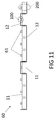
- FIG 11 schematically shows a cross section of a second exemplary woven fabric 60. More in particular, FIG 11 shows a cross section along the weft direction 3, i.e. substantially orthogonal to the warp direction 2, of such a woven fabric 60.
- the woven fabric 60 comprises a plurality of electrically insulating ribbons 11 arranged in the warp direction, a first plurality of first electrically conductive wires or ribbons 12 arranged in the weft direction and a second plurality of second electrically conductive wires or ribbons 61 arranged in the warp direction.
- the width of the second electrically conductive ribbons 61 is substantially smaller than the width of the electrically insulating ribbons 11, and each one of the plurality of second electrically conductive ribbons 61 is provided on, i.e. stacked on, e.g. coated on, and laterally aligned with, an electrically insulating ribbon 11 such that its lateral edges are not extending beyond lateral edges of the electrically insulating ribbon 11.
- the plurality of second electrically conductive ribbons 61 is provided at a single side (at the second side or non-contact side) of the woven fabric, i.e. at a single side of the plurality of electrically insulating ribbons.
- the second electrically conductive wires, e.g. ribbons, 61 may be provided in the fabric by stacking them, e.g. coating them, on the electrically insulating ribbons.
- the first electrically conductive wires, e.g. ribbons, 12 may be secured in the woven fabric by weaving them (thereby providing them in the weft direction) with the plurality of electrically insulating ribbons 11 coated at a second side with an electrically conductive wire or ribbons 61.
- an electrical contact or electrical connection may be formed between a first electrically conductive wire or ribbon 12 and a second electrically conductive wire or ribbon 61 at locations 100 where the first electrically conductive wire 12 is exposed at the second side of the fabric, as illustrated in FIG 11 .
- an electrically insulating ribbon 11 electrically insulates the second electrically conductive wire 61 from the first electrically conductive wire 12 provided on the electrically insulating ribbon, and at such locations 200 no electrical contact is formed between the first and second electrically conductive ribbons. This is illustrated in FIG 11 .
- a twill fabric may be used wherein the first electrically conductive wires 12 are woven in pairs 122 into the fabric 60, i.e. wherein pairs 122 of first electrically conductive wires are woven into the fabric, each pair 122 comprising two first electrically conductive wires 12 woven side by side (next to each other but with a lateral spacing in between) into the fabric 60 according to the same pattern (i.e. passing over and under the same warp oriented ribbons).
- the two first electrically conductive wires of each pair 122 may be electrically connected to a same, single, second electrically conductive wire 61, e.g.
- the second electrically conductive wire 61 may be interrupted between both these locations 100 to electrically insulate the first electrically conductive wires from the same pair from each other. Interrupting of the second electrically conductive wire may for example be obtained by punching or cutting a hole 15 through the second electrically conductive wire. As a result of this interrupting, e.g. hole punching or hole cutting, the second electrically conductive wire comprises, e.g. is divided into, at least a first segment and a second segment that are electrically insulated from each other.
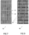
- FIG 7 illustrates, schematically, a back surface of an exemplary interdigitated back-contact photovoltaic cell 70, for use in combination with an exemplary woven fabric 60 in accordance with embodiments of the present invention as shown in FIG 6 .
- the photovoltaic cell 70 comprises, on the surface for contacting the woven fabric, e.g. on the rear surface opposite of the front surface for being oriented to a source of illumination in operation of the cell, at least one first metal contact 21 and at least one second metal contact 22 of opposite polarity with respect to the first metal contact.
- a plurality of first contacts 21 may consist of first busbars and a plurality of first fingers electrically connected thereto for connecting to a first polarity
- the plurality of second contacts 22 may consist of second busbars and a plurality of second fingers electrically connected thereto for connecting to the opposite polarity, wherein the plurality of first fingers are interdigitated with the plurality of second fingers.
- embodiments of the present invention are not necessarily limited to IBC cells comprising busbar structures.
- the woven fabric 60 may be used to locally form busbar structures connecting directly to first and second contacts formed by the cell finger structures.
- the woven fabric 60 comprises a plurality of electrically insulating ribbons 11 arranged in a warp direction 2 of the woven fabric.
- the woven fabric 60 also comprises a first plurality of first electrically conductive wires 12, arranged in the weft direction 3 of the woven fabric and a second plurality of second electrically conductive wires 61 arranged in a warp direction 2 of the woven fabric.
- a second electrically conductive wire 61 may be provided on top of the insulating ribbon, e.g. arranged substantially along a central longitudinal axis thereof and in direct physical contact with the insulating ribbon at the 'non-contact' side thereof, e.g.
- the second plurality of conductive wires 61 may be provided to form cell-to-cell interconnections in a cell string, while the first plurality of first conductive wires 12 may be provided to form an electrical connection to contacts 21, 22 of the photovoltaic cell 70 and to form an electrical connection to a segment of a conductive wire of the second plurality of second conductive wires 61. Furthermore, the first plurality of conductive wires 12 may provide interconnections between a plurality of cell strings, e.g. for interconnecting two cell strings.
- the woven fabric 60 may be a twill or twill-like weave fabric, the present invention not being limited thereto.
- This twill or twill-like pattern may advantageously implement a tapering design, as will be described hereinbelow.
- at least two, e.g. two, conductive wires of the first plurality of first conductive wires 12 may be weft per pick, e.g. such as to provide pairs of adjacent conductive wires in the weft direction that are aligned with respect to the weave pattern.
- the woven fabric 60 may be a twill weave pattern with double weft conducting wires 12, and may be identified by a twill ratio of x/y, where x, the number of harnesses lifted in the loom, equals the number of busbars of same polarity on the photovoltaic cell minus one, and where y, the number of harnesses lowered in the loom, equals 1.
- a 3/1 warp-face twill, e.g. 1 up and 3 down, of double weft conductive wires may be provided.
- the first plurality of first conductive wires 12 may be woven such that a twill pattern exposes a conductive wire of the first plurality of conductive wires 12 at a surface for contacting the photovoltaic cell at a first predetermined location 16 corresponding to a location of a first contact 21 on the photovoltaic cell 70, and for exposing another conductive wire of the first plurality of first conductive wires 12 at this surface for contacting at a second predetermined location 17 corresponding to a location of a second contact 22.
- This pair 122 of conductive wires may be adjacent, e.g. neighbouring conductive wires in the weft direction, i.e. they may form a pair 122 of first electrically conductive wires.
- This pair 122 of first electrically conductive wires 12 may furthermore be aligned with respect to the weave pattern, e.g. may correspond to a single pick of double weft conductive wires. Where both conductive wires cross over a common insulating ribbon, e.g. due to their aligned weave, an electrical connection would be established between the first contact 21 and the second contact 22 via the first and second conductive wires. However, an electrical interruption, e.g. a hole 15, in between the double weft conductive wires, is provided in the second conductive wire 61 in the warp direction to electrically insulate the first contact 21 and the second contact 22 from each other.
- an electrical interruption e.g. a hole 15, in between the double weft conductive wires
- At least one of, e.g. most of or each of, the plurality of second electrically conductive wires 61 comprises at least a first segment 13 and a second segment 14 that are electrically insulated from each other, e.g. by a hole 15 separating the first segment 13 from the second segment 14.
- most of, e.g. each of, the second plurality of second conductive wires 61 may be severed or interrupted by a corresponding hole 15 provided through the conductive wire 61 and the insulating ribbon 11 directly underneath.
- Such hole may be provided by stamping or locally cutting the conductive wire 61, e.g. stamping or cutting the conductive wire and the overlapping part of the insulating ribbon.
- the width of the hole 15 may be smaller than the width of the insulating ribbon, e.g. such as to maintain a structural integrity provided by the warp oriented ribbon.
- Such electrical interruption may be provided at a location in between the locations where the respective first conductive ribbons or wires 12 of a pair 122 of conductive wires for contacting the photovoltaic cell at respectively the first predetermined location 16 and the second predetermined location 17 cross over at least one insulating ribbon 11, e.g. over the same insulating ribbon, such that the first segment 13 electrically connects to one conductive wire of this pair 122, and the second segment 14 electrically connects to the other conductive wire of this pair 122.
- a hole 15, or a different type of electrical interruption for at least electrically disconnecting the first segment from the second segment may be provided through the first electrically conductive wire 61 in between the wires 12 of the pair 122 of aligned weft second electrically conductive wires 12.
- each second electrically conductive wire 61 may be provided in each second electrically conductive wire 61 at a fixed position with respect to the twill-like weave pattern, e.g. in a fixed pick of the pick sequence. Due to a fixed offset of the weave pattern, e.g. the pick pattern, in one conductive wire pair with respect to a next wire pair, the electrical interruptions may form a tapered structure in the woven fabric.
- each second electrically conductive wire 61 may comprise a segment for contacting a negative polarity contact of the photovoltaic cell at one end and a segment for contacting a positive polarity contact of the photovoltaic cell at the other end.
- a method in accordance with embodiments of the present invention may comprise aligning the at least one photovoltaic cell 70 and the woven fabric 60, e.g. prior to bringing the woven fabric into contact with the photovoltaic cell, such as to align the first predetermined location 16 with a location of a first contact 21 on the photovoltaic cell 70, and to align the second predetermined location 17 with a location of a second contact 22.
- first segments 13 of the second electrically conductive wires 61 may be electrically connected to the photovoltaic cells to carry a first charge polarity, e.g. connected to '-' terminals, and second segments 14 of the second electrically conductive wires 61 may be electrically connected to the photovoltaic cells to carry a second charge polarity opposite to the first charge polarity, e.g. connected to '+' terminals.
- the photovoltaic cell or a plurality of photovoltaic cells 70 may be provided on, e.g. laid on, a transparent front carrier such as a glass plate, with a front side of the photovoltaic cells being oriented towards the front carrier, the woven fabric 60 may be provided on, e.g. laid on, the photovoltaic cells and aligned with the photovoltaic cells, and a back carrier, e.g. a further glass plate or backsheet, may be provided on, e.g. laid on, the woven fabric, in view of forming an encapsulated photovoltaic module.
- an encapsulant e.g. a transparent encapsulant, may be provided in between the transparent front carrier and the photovoltaic cells.
- the material of the insulating ribbons of the woven fabric 60 may function as an encapsulant.
- the amount of encapsulation material provided by the insulating ribbons 11 may be sufficient, i.e. there may be no need for providing additional encapsulation material or an additional encapsulation layer.
- a heating process is performed, thereby transforming the material of the electrically insulating ribbons into an encapsulant layer, e.g. by liquefying the insulating ribbons.
- the photovoltaic cells 70 are electrically connected and physically bonded to the woven fabric 60.
- FIG 9 shows a busbar-less interdigitated back-contact photovoltaic cell 90.
- the cell-level busbar function may be replaced by the first plurality of conductive wires 12 in the woven fabric 60, e.g. by directly soldering the contact-side exposed wires of the first plurality of conductive wires 12 on the cell fingers.
- fingers may be joined by a local metal connection on the photovoltaic cell 90 at locations 91 where the first plurality of conductive wires are not exposed at the contact-side of the woven fabric, as shown by the alignment and contacting steps depicted in FIG 10 .
Landscapes
- Engineering & Computer Science (AREA)
- Manufacturing & Machinery (AREA)
- Photovoltaic Devices (AREA)
- Life Sciences & Earth Sciences (AREA)
- Sustainable Development (AREA)
- Sustainable Energy (AREA)
Priority Applications (3)
| Application Number | Priority Date | Filing Date | Title |
|---|---|---|---|
| KR1020170072452A KR20170142888A (ko) | 2016-06-17 | 2017-06-09 | 광전지를 전기적으로 접촉하기 위한 하이브리드 위브 |
| JP2017114523A JP6986866B2 (ja) | 2016-06-17 | 2017-06-09 | 光発電セルを電気的に接触させるためのハイブリッドな織り方 |
| CN201710451463.3A CN107527965B (zh) | 2016-06-17 | 2017-06-15 | 用于电接触光伏电池的混合编织 |
Applications Claiming Priority (1)
| Application Number | Priority Date | Filing Date | Title |
|---|---|---|---|
| EP16175066 | 2016-06-17 |
Publications (2)
| Publication Number | Publication Date |
|---|---|
| EP3258503A1 true EP3258503A1 (de) | 2017-12-20 |
| EP3258503B1 EP3258503B1 (de) | 2023-04-12 |
Family
ID=56134265
Family Applications (1)
| Application Number | Title | Priority Date | Filing Date |
|---|---|---|---|
| EP16180461.2A Active EP3258503B1 (de) | 2016-06-17 | 2016-07-20 | Mischgewebe zur elektrischen kontaktierung von photovoltaischen zellen |
Country Status (4)
| Country | Link |
|---|---|
| EP (1) | EP3258503B1 (de) |
| JP (1) | JP6986866B2 (de) |
| KR (1) | KR20170142888A (de) |
| CN (1) | CN107527965B (de) |
Cited By (5)
| Publication number | Priority date | Publication date | Assignee | Title |
|---|---|---|---|---|
| EP3790059A1 (de) | 2019-09-05 | 2021-03-10 | Imec VZW | Verfahren zur elektrischen kontaktierung und verbindung von fotovoltaischen zellen |
| CN114649436A (zh) * | 2022-05-20 | 2022-06-21 | 英利能源发展有限公司 | 一种新型光伏组件及其制备方法 |
| CN114649443A (zh) * | 2022-03-03 | 2022-06-21 | 浙江爱旭太阳能科技有限公司 | 背接触太阳能电池串及其制备方法、电池组件及光伏系统 |
| EP4325585A1 (de) * | 2022-08-16 | 2024-02-21 | Imec VZW | Verfahren zum kontinuierlichen aufreihen von fotovoltaischen zellen und zusammenbau von fotovoltaischen zellen |
| CN119050187A (zh) * | 2024-08-29 | 2024-11-29 | 浙江爱旭太阳能科技有限公司 | 一种背接触电池组件和光伏系统 |
Families Citing this family (3)
| Publication number | Priority date | Publication date | Assignee | Title |
|---|---|---|---|---|
| DE102018213911A1 (de) * | 2018-08-17 | 2020-02-20 | Robert Bosch Gmbh | Zellkontaktierungssystem für eine modular aufgebaute Batterie |
| PL3723206T3 (pl) * | 2019-04-08 | 2023-02-06 | Vibia Lighting S.L. | Urządzenie elektryczne podłączane do przewodzącej taśmy tkaniny |
| EP3817070B1 (de) * | 2019-10-31 | 2023-06-28 | CSEM Centre Suisse D'electronique Et De Microtechnique SA | Verfahren zur herstellung einer fotovoltaikvorrichtung |
Citations (3)
| Publication number | Priority date | Publication date | Assignee | Title |
|---|---|---|---|---|
| WO2012173487A1 (en) * | 2011-06-17 | 2012-12-20 | Stichting Onderzoek Centrum Nederland | Photovoltaic system and connector for a photovoltaic cell with interdigitated contacts |
| EP2660878A1 (de) | 2012-05-04 | 2013-11-06 | Sol Invictus Energy | Hybride Webmaterialien zur Herstellung von Solarzellen mit hinterem Kontakt |
| US20150340529A1 (en) * | 2012-12-18 | 2015-11-26 | Commissariat à l'Energie Atomique et aux Energies Alternatives | Device for interconnecting photovoltaic cells having contacts on their back side, and module comprising such a device |
Family Cites Families (3)
| Publication number | Priority date | Publication date | Assignee | Title |
|---|---|---|---|---|
| DE102010016675A1 (de) * | 2010-04-28 | 2011-11-03 | Solarworld Innovations Gmbh | Photovoltaikmodul, Verfahren zum elektrischen Verbinden einer Mehrzahl von Photovoltaikzellen, und Einrichtung zum elektrischen Verbinden einer Mehrzahl von Photovoltaikzellen |
| CN104319301A (zh) * | 2014-09-28 | 2015-01-28 | 苏州中来光伏新材股份有限公司 | 无主栅、高效率背接触太阳能电池背板、组件及制备工艺 |
| CN204204885U (zh) * | 2014-09-28 | 2015-03-11 | 苏州中来光伏新材股份有限公司 | 无主栅高效率背接触太阳能电池背板 |
-
2016
- 2016-07-20 EP EP16180461.2A patent/EP3258503B1/de active Active
-
2017
- 2017-06-09 JP JP2017114523A patent/JP6986866B2/ja active Active
- 2017-06-09 KR KR1020170072452A patent/KR20170142888A/ko not_active Withdrawn
- 2017-06-15 CN CN201710451463.3A patent/CN107527965B/zh active Active
Patent Citations (3)
| Publication number | Priority date | Publication date | Assignee | Title |
|---|---|---|---|---|
| WO2012173487A1 (en) * | 2011-06-17 | 2012-12-20 | Stichting Onderzoek Centrum Nederland | Photovoltaic system and connector for a photovoltaic cell with interdigitated contacts |
| EP2660878A1 (de) | 2012-05-04 | 2013-11-06 | Sol Invictus Energy | Hybride Webmaterialien zur Herstellung von Solarzellen mit hinterem Kontakt |
| US20150340529A1 (en) * | 2012-12-18 | 2015-11-26 | Commissariat à l'Energie Atomique et aux Energies Alternatives | Device for interconnecting photovoltaic cells having contacts on their back side, and module comprising such a device |
Cited By (7)
| Publication number | Priority date | Publication date | Assignee | Title |
|---|---|---|---|---|
| EP3790059A1 (de) | 2019-09-05 | 2021-03-10 | Imec VZW | Verfahren zur elektrischen kontaktierung und verbindung von fotovoltaischen zellen |
| CN114649443A (zh) * | 2022-03-03 | 2022-06-21 | 浙江爱旭太阳能科技有限公司 | 背接触太阳能电池串及其制备方法、电池组件及光伏系统 |
| CN114649443B (zh) * | 2022-03-03 | 2024-04-16 | 浙江爱旭太阳能科技有限公司 | 背接触太阳能电池串及其制备方法、电池组件及光伏系统 |
| CN114649436A (zh) * | 2022-05-20 | 2022-06-21 | 英利能源发展有限公司 | 一种新型光伏组件及其制备方法 |
| CN114649436B (zh) * | 2022-05-20 | 2022-08-23 | 英利能源发展有限公司 | 一种新型光伏组件及其制备方法 |
| EP4325585A1 (de) * | 2022-08-16 | 2024-02-21 | Imec VZW | Verfahren zum kontinuierlichen aufreihen von fotovoltaischen zellen und zusammenbau von fotovoltaischen zellen |
| CN119050187A (zh) * | 2024-08-29 | 2024-11-29 | 浙江爱旭太阳能科技有限公司 | 一种背接触电池组件和光伏系统 |
Also Published As
| Publication number | Publication date |
|---|---|
| KR20170142888A (ko) | 2017-12-28 |
| JP6986866B2 (ja) | 2021-12-22 |
| CN107527965B (zh) | 2022-05-10 |
| EP3258503B1 (de) | 2023-04-12 |
| JP2017224817A (ja) | 2017-12-21 |
| CN107527965A (zh) | 2017-12-29 |
Similar Documents
| Publication | Publication Date | Title |
|---|---|---|
| EP3258503B1 (de) | Mischgewebe zur elektrischen kontaktierung von photovoltaischen zellen | |
| CN103038896B (zh) | 用于接通和连接太阳能电池的方法和太阳能电池组合体 | |
| US8253213B2 (en) | Photoelectric conversion element, photoelectric conversion element assembly and photoelectric conversion module | |
| US20080236655A1 (en) | Solar module manufacturing processes | |
| US20080216887A1 (en) | Interconnect Technologies for Back Contact Solar Cells and Modules | |
| JP2024516468A (ja) | 裏面接触太陽電池ストリング及びその製造方法、アセンブリ並びにシステム | |
| WO2011011855A1 (en) | Method for interconnecting back contact solar cells and photovoltaic module employing same | |
| US12183840B2 (en) | Solar cell and solar cell module | |
| CN104919597A (zh) | 用于太阳能电池串的高效配置 | |
| EP3278370B1 (de) | Elektrische kontaktierung und verbindung von photovoltaikzellen | |
| US9490377B2 (en) | Use of a uniform layer of insulating material in back-contact solar cells | |
| CN101390220A (zh) | 高压太阳能电池和太阳能电池模块 | |
| US20150155398A1 (en) | Photovoltaic monolithic solar module connection and fabrication methods | |
| CN114388636B (zh) | 一种背接触电池串、背接触电池组件以及背接触电池系统 | |
| CN111201615B (zh) | 用于将单个太阳能电池互连成太阳能电池模块的胶带 | |
| EP3235012B1 (de) | Verfahren zur verbindung von photovoltaikzellen mit hinterkontakt | |
| CN110707167A (zh) | 背接触太阳能电池组件生产方法及背接触太阳能电池组件 | |
| JP2024109947A (ja) | クリーブ加工された縁部から後退した接合部を有する太陽電池 | |
| Borgers et al. | Multi-wire interconnection technologies weaving the way for back contact and bifacial PV modules | |
| US20210313479A1 (en) | High Power Density Solar Module and Methods of Fabrication | |
| EP3790059A1 (de) | Verfahren zur elektrischen kontaktierung und verbindung von fotovoltaischen zellen | |
| WO2017093527A1 (en) | Interconnection of back-contacted solar cell, a solar panel having such interconnection | |
| KR101153591B1 (ko) | 결정질 실리콘 태양전지의 구조 및 제조방법 | |
| KR102233683B1 (ko) | 와이어를 구비한 슁글드 태양전지 패널 및 그 제조방법 | |
| Van Dyck et al. | Woven multi-ribbon interconnection for back-contact cells: Extending the functionality of the encapsulant |
Legal Events
| Date | Code | Title | Description |
|---|---|---|---|
| PUAI | Public reference made under article 153(3) epc to a published international application that has entered the european phase |
Free format text: ORIGINAL CODE: 0009012 |
|
| STAA | Information on the status of an ep patent application or granted ep patent |
Free format text: STATUS: THE APPLICATION HAS BEEN PUBLISHED |
|
| AK | Designated contracting states |
Kind code of ref document: A1 Designated state(s): AL AT BE BG CH CY CZ DE DK EE ES FI FR GB GR HR HU IE IS IT LI LT LU LV MC MK MT NL NO PL PT RO RS SE SI SK SM TR |
|
| AX | Request for extension of the european patent |
Extension state: BA ME |
|
| RBV | Designated contracting states (corrected) |
Designated state(s): AL AT BE BG CH CY CZ DE DK EE ES FI FR GB GR HR HU IE IS IT LI LT LU LV MC MK MT NL NO PL PT RO RS SE SI SK SM TR |
|
| STAA | Information on the status of an ep patent application or granted ep patent |
Free format text: STATUS: REQUEST FOR EXAMINATION WAS MADE |
|
| 17P | Request for examination filed |
Effective date: 20180613 |
|
| STAA | Information on the status of an ep patent application or granted ep patent |
Free format text: STATUS: EXAMINATION IS IN PROGRESS |
|
| 17Q | First examination report despatched |
Effective date: 20190322 |
|
| GRAP | Despatch of communication of intention to grant a patent |
Free format text: ORIGINAL CODE: EPIDOSNIGR1 |
|
| STAA | Information on the status of an ep patent application or granted ep patent |
Free format text: STATUS: GRANT OF PATENT IS INTENDED |
|
| RIC1 | Information provided on ipc code assigned before grant |
Ipc: H01R 43/02 20060101ALI20211109BHEP Ipc: H01L 31/05 20140101ALI20211109BHEP Ipc: H01L 31/0224 20060101ALI20211109BHEP Ipc: H01R 4/02 20060101ALI20211109BHEP Ipc: H01L 31/048 20140101AFI20211109BHEP |
|
| INTG | Intention to grant announced |
Effective date: 20211130 |
|
| GRAJ | Information related to disapproval of communication of intention to grant by the applicant or resumption of examination proceedings by the epo deleted |
Free format text: ORIGINAL CODE: EPIDOSDIGR1 |
|
| STAA | Information on the status of an ep patent application or granted ep patent |
Free format text: STATUS: EXAMINATION IS IN PROGRESS |
|
| GRAP | Despatch of communication of intention to grant a patent |
Free format text: ORIGINAL CODE: EPIDOSNIGR1 |
|
| STAA | Information on the status of an ep patent application or granted ep patent |
Free format text: STATUS: GRANT OF PATENT IS INTENDED |
|
| INTC | Intention to grant announced (deleted) | ||
| INTG | Intention to grant announced |
Effective date: 20220509 |
|
| GRAJ | Information related to disapproval of communication of intention to grant by the applicant or resumption of examination proceedings by the epo deleted |
Free format text: ORIGINAL CODE: EPIDOSDIGR1 |
|
| STAA | Information on the status of an ep patent application or granted ep patent |
Free format text: STATUS: EXAMINATION IS IN PROGRESS |
|
| GRAP | Despatch of communication of intention to grant a patent |
Free format text: ORIGINAL CODE: EPIDOSNIGR1 |
|
| STAA | Information on the status of an ep patent application or granted ep patent |
Free format text: STATUS: GRANT OF PATENT IS INTENDED |
|
| INTC | Intention to grant announced (deleted) | ||
| INTG | Intention to grant announced |
Effective date: 20221019 |
|
| GRAS | Grant fee paid |
Free format text: ORIGINAL CODE: EPIDOSNIGR3 |
|
| GRAA | (expected) grant |
Free format text: ORIGINAL CODE: 0009210 |
|
| STAA | Information on the status of an ep patent application or granted ep patent |
Free format text: STATUS: THE PATENT HAS BEEN GRANTED |
|
| AK | Designated contracting states |
Kind code of ref document: B1 Designated state(s): AL AT BE BG CH CY CZ DE DK EE ES FI FR GB GR HR HU IE IS IT LI LT LU LV MC MK MT NL NO PL PT RO RS SE SI SK SM TR |
|
| REG | Reference to a national code |
Ref country code: GB Ref legal event code: FG4D |
|
| REG | Reference to a national code |
Ref country code: CH Ref legal event code: EP |
|
| REG | Reference to a national code |
Ref country code: DE Ref legal event code: R096 Ref document number: 602016078767 Country of ref document: DE |
|
| REG | Reference to a national code |
Ref country code: IE Ref legal event code: FG4D |
|
| REG | Reference to a national code |
Ref country code: AT Ref legal event code: REF Ref document number: 1560266 Country of ref document: AT Kind code of ref document: T Effective date: 20230515 |
|
| P01 | Opt-out of the competence of the unified patent court (upc) registered |
Effective date: 20230513 |
|
| REG | Reference to a national code |
Ref country code: LT Ref legal event code: MG9D |
|
| REG | Reference to a national code |
Ref country code: NL Ref legal event code: MP Effective date: 20230412 |
|
| REG | Reference to a national code |
Ref country code: AT Ref legal event code: MK05 Ref document number: 1560266 Country of ref document: AT Kind code of ref document: T Effective date: 20230412 |
|
| PG25 | Lapsed in a contracting state [announced via postgrant information from national office to epo] |
Ref country code: NL Free format text: LAPSE BECAUSE OF FAILURE TO SUBMIT A TRANSLATION OF THE DESCRIPTION OR TO PAY THE FEE WITHIN THE PRESCRIBED TIME-LIMIT Effective date: 20230412 |
|
| PG25 | Lapsed in a contracting state [announced via postgrant information from national office to epo] |
Ref country code: SE Free format text: LAPSE BECAUSE OF FAILURE TO SUBMIT A TRANSLATION OF THE DESCRIPTION OR TO PAY THE FEE WITHIN THE PRESCRIBED TIME-LIMIT Effective date: 20230412 Ref country code: PT Free format text: LAPSE BECAUSE OF FAILURE TO SUBMIT A TRANSLATION OF THE DESCRIPTION OR TO PAY THE FEE WITHIN THE PRESCRIBED TIME-LIMIT Effective date: 20230814 Ref country code: NO Free format text: LAPSE BECAUSE OF FAILURE TO SUBMIT A TRANSLATION OF THE DESCRIPTION OR TO PAY THE FEE WITHIN THE PRESCRIBED TIME-LIMIT Effective date: 20230712 Ref country code: ES Free format text: LAPSE BECAUSE OF FAILURE TO SUBMIT A TRANSLATION OF THE DESCRIPTION OR TO PAY THE FEE WITHIN THE PRESCRIBED TIME-LIMIT Effective date: 20230412 Ref country code: AT Free format text: LAPSE BECAUSE OF FAILURE TO SUBMIT A TRANSLATION OF THE DESCRIPTION OR TO PAY THE FEE WITHIN THE PRESCRIBED TIME-LIMIT Effective date: 20230412 |
|
| PG25 | Lapsed in a contracting state [announced via postgrant information from national office to epo] |
Ref country code: RS Free format text: LAPSE BECAUSE OF FAILURE TO SUBMIT A TRANSLATION OF THE DESCRIPTION OR TO PAY THE FEE WITHIN THE PRESCRIBED TIME-LIMIT Effective date: 20230412 Ref country code: PL Free format text: LAPSE BECAUSE OF FAILURE TO SUBMIT A TRANSLATION OF THE DESCRIPTION OR TO PAY THE FEE WITHIN THE PRESCRIBED TIME-LIMIT Effective date: 20230412 Ref country code: LV Free format text: LAPSE BECAUSE OF FAILURE TO SUBMIT A TRANSLATION OF THE DESCRIPTION OR TO PAY THE FEE WITHIN THE PRESCRIBED TIME-LIMIT Effective date: 20230412 Ref country code: LT Free format text: LAPSE BECAUSE OF FAILURE TO SUBMIT A TRANSLATION OF THE DESCRIPTION OR TO PAY THE FEE WITHIN THE PRESCRIBED TIME-LIMIT Effective date: 20230412 Ref country code: IS Free format text: LAPSE BECAUSE OF FAILURE TO SUBMIT A TRANSLATION OF THE DESCRIPTION OR TO PAY THE FEE WITHIN THE PRESCRIBED TIME-LIMIT Effective date: 20230812 Ref country code: HR Free format text: LAPSE BECAUSE OF FAILURE TO SUBMIT A TRANSLATION OF THE DESCRIPTION OR TO PAY THE FEE WITHIN THE PRESCRIBED TIME-LIMIT Effective date: 20230412 Ref country code: GR Free format text: LAPSE BECAUSE OF FAILURE TO SUBMIT A TRANSLATION OF THE DESCRIPTION OR TO PAY THE FEE WITHIN THE PRESCRIBED TIME-LIMIT Effective date: 20230713 Ref country code: AL Free format text: LAPSE BECAUSE OF FAILURE TO SUBMIT A TRANSLATION OF THE DESCRIPTION OR TO PAY THE FEE WITHIN THE PRESCRIBED TIME-LIMIT Effective date: 20230412 |
|
| PG25 | Lapsed in a contracting state [announced via postgrant information from national office to epo] |
Ref country code: FI Free format text: LAPSE BECAUSE OF FAILURE TO SUBMIT A TRANSLATION OF THE DESCRIPTION OR TO PAY THE FEE WITHIN THE PRESCRIBED TIME-LIMIT Effective date: 20230412 |
|
| REG | Reference to a national code |
Ref country code: DE Ref legal event code: R097 Ref document number: 602016078767 Country of ref document: DE |
|
| PG25 | Lapsed in a contracting state [announced via postgrant information from national office to epo] |
Ref country code: SK Free format text: LAPSE BECAUSE OF FAILURE TO SUBMIT A TRANSLATION OF THE DESCRIPTION OR TO PAY THE FEE WITHIN THE PRESCRIBED TIME-LIMIT Effective date: 20230412 |
|
| PG25 | Lapsed in a contracting state [announced via postgrant information from national office to epo] |
Ref country code: SM Free format text: LAPSE BECAUSE OF FAILURE TO SUBMIT A TRANSLATION OF THE DESCRIPTION OR TO PAY THE FEE WITHIN THE PRESCRIBED TIME-LIMIT Effective date: 20230412 Ref country code: SK Free format text: LAPSE BECAUSE OF FAILURE TO SUBMIT A TRANSLATION OF THE DESCRIPTION OR TO PAY THE FEE WITHIN THE PRESCRIBED TIME-LIMIT Effective date: 20230412 Ref country code: RO Free format text: LAPSE BECAUSE OF FAILURE TO SUBMIT A TRANSLATION OF THE DESCRIPTION OR TO PAY THE FEE WITHIN THE PRESCRIBED TIME-LIMIT Effective date: 20230412 Ref country code: EE Free format text: LAPSE BECAUSE OF FAILURE TO SUBMIT A TRANSLATION OF THE DESCRIPTION OR TO PAY THE FEE WITHIN THE PRESCRIBED TIME-LIMIT Effective date: 20230412 Ref country code: DK Free format text: LAPSE BECAUSE OF FAILURE TO SUBMIT A TRANSLATION OF THE DESCRIPTION OR TO PAY THE FEE WITHIN THE PRESCRIBED TIME-LIMIT Effective date: 20230412 Ref country code: CZ Free format text: LAPSE BECAUSE OF FAILURE TO SUBMIT A TRANSLATION OF THE DESCRIPTION OR TO PAY THE FEE WITHIN THE PRESCRIBED TIME-LIMIT Effective date: 20230412 |
|
| PLBE | No opposition filed within time limit |
Free format text: ORIGINAL CODE: 0009261 |
|
| STAA | Information on the status of an ep patent application or granted ep patent |
Free format text: STATUS: NO OPPOSITION FILED WITHIN TIME LIMIT |
|
| PG25 | Lapsed in a contracting state [announced via postgrant information from national office to epo] |
Ref country code: MC Free format text: LAPSE BECAUSE OF FAILURE TO SUBMIT A TRANSLATION OF THE DESCRIPTION OR TO PAY THE FEE WITHIN THE PRESCRIBED TIME-LIMIT Effective date: 20230412 |
|
| PG25 | Lapsed in a contracting state [announced via postgrant information from national office to epo] |
Ref country code: MC Free format text: LAPSE BECAUSE OF FAILURE TO SUBMIT A TRANSLATION OF THE DESCRIPTION OR TO PAY THE FEE WITHIN THE PRESCRIBED TIME-LIMIT Effective date: 20230412 |
|
| REG | Reference to a national code |
Ref country code: CH Ref legal event code: PL |
|
| REG | Reference to a national code |
Ref country code: BE Ref legal event code: MM Effective date: 20230731 |
|
| 26N | No opposition filed |
Effective date: 20240115 |
|
| PG25 | Lapsed in a contracting state [announced via postgrant information from national office to epo] |
Ref country code: LU Free format text: LAPSE BECAUSE OF NON-PAYMENT OF DUE FEES Effective date: 20230720 |
|
| GBPC | Gb: european patent ceased through non-payment of renewal fee |
Effective date: 20230720 |
|
| PG25 | Lapsed in a contracting state [announced via postgrant information from national office to epo] |
Ref country code: LU Free format text: LAPSE BECAUSE OF NON-PAYMENT OF DUE FEES Effective date: 20230720 |
|
| REG | Reference to a national code |
Ref country code: IE Ref legal event code: MM4A |
|
| PG25 | Lapsed in a contracting state [announced via postgrant information from national office to epo] |
Ref country code: CH Free format text: LAPSE BECAUSE OF NON-PAYMENT OF DUE FEES Effective date: 20230731 Ref country code: GB Free format text: LAPSE BECAUSE OF NON-PAYMENT OF DUE FEES Effective date: 20230720 |
|
| PG25 | Lapsed in a contracting state [announced via postgrant information from national office to epo] |
Ref country code: SI Free format text: LAPSE BECAUSE OF FAILURE TO SUBMIT A TRANSLATION OF THE DESCRIPTION OR TO PAY THE FEE WITHIN THE PRESCRIBED TIME-LIMIT Effective date: 20230412 |
|
| PG25 | Lapsed in a contracting state [announced via postgrant information from national office to epo] |
Ref country code: SI Free format text: LAPSE BECAUSE OF FAILURE TO SUBMIT A TRANSLATION OF THE DESCRIPTION OR TO PAY THE FEE WITHIN THE PRESCRIBED TIME-LIMIT Effective date: 20230412 Ref country code: FR Free format text: LAPSE BECAUSE OF NON-PAYMENT OF DUE FEES Effective date: 20230731 Ref country code: BE Free format text: LAPSE BECAUSE OF NON-PAYMENT OF DUE FEES Effective date: 20230731 |
|
| PG25 | Lapsed in a contracting state [announced via postgrant information from national office to epo] |
Ref country code: IE Free format text: LAPSE BECAUSE OF NON-PAYMENT OF DUE FEES Effective date: 20230720 |
|
| PG25 | Lapsed in a contracting state [announced via postgrant information from national office to epo] |
Ref country code: IE Free format text: LAPSE BECAUSE OF NON-PAYMENT OF DUE FEES Effective date: 20230720 |
|
| PG25 | Lapsed in a contracting state [announced via postgrant information from national office to epo] |
Ref country code: BG Free format text: LAPSE BECAUSE OF FAILURE TO SUBMIT A TRANSLATION OF THE DESCRIPTION OR TO PAY THE FEE WITHIN THE PRESCRIBED TIME-LIMIT Effective date: 20230412 |
|
| REG | Reference to a national code |
Ref country code: DE Ref legal event code: R079 Ref document number: 602016078767 Country of ref document: DE Free format text: PREVIOUS MAIN CLASS: H01L0031048000 Ipc: H10F0019800000 |
|
| PG25 | Lapsed in a contracting state [announced via postgrant information from national office to epo] |
Ref country code: BG Free format text: LAPSE BECAUSE OF FAILURE TO SUBMIT A TRANSLATION OF THE DESCRIPTION OR TO PAY THE FEE WITHIN THE PRESCRIBED TIME-LIMIT Effective date: 20230412 |
|
| PG25 | Lapsed in a contracting state [announced via postgrant information from national office to epo] |
Ref country code: CY Free format text: LAPSE BECAUSE OF FAILURE TO SUBMIT A TRANSLATION OF THE DESCRIPTION OR TO PAY THE FEE WITHIN THE PRESCRIBED TIME-LIMIT; INVALID AB INITIO Effective date: 20160720 |
|
| PG25 | Lapsed in a contracting state [announced via postgrant information from national office to epo] |
Ref country code: HU Free format text: LAPSE BECAUSE OF FAILURE TO SUBMIT A TRANSLATION OF THE DESCRIPTION OR TO PAY THE FEE WITHIN THE PRESCRIBED TIME-LIMIT; INVALID AB INITIO Effective date: 20160720 |
|
| PGFP | Annual fee paid to national office [announced via postgrant information from national office to epo] |
Ref country code: DE Payment date: 20250620 Year of fee payment: 10 |
|
| PGFP | Annual fee paid to national office [announced via postgrant information from national office to epo] |
Ref country code: IT Payment date: 20250619 Year of fee payment: 10 |
|
| PG25 | Lapsed in a contracting state [announced via postgrant information from national office to epo] |
Ref country code: TR Free format text: LAPSE BECAUSE OF FAILURE TO SUBMIT A TRANSLATION OF THE DESCRIPTION OR TO PAY THE FEE WITHIN THE PRESCRIBED TIME-LIMIT Effective date: 20230412 |