EP3258492A1 - Image-capture element - Google Patents
Image-capture element Download PDFInfo
- Publication number
- EP3258492A1 EP3258492A1 EP15882012.6A EP15882012A EP3258492A1 EP 3258492 A1 EP3258492 A1 EP 3258492A1 EP 15882012 A EP15882012 A EP 15882012A EP 3258492 A1 EP3258492 A1 EP 3258492A1
- Authority
- EP
- European Patent Office
- Prior art keywords
- transfer
- electrode
- column
- transistor
- diffusion layer
- Prior art date
- Legal status (The legal status is an assumption and is not a legal conclusion. Google has not performed a legal analysis and makes no representation as to the accuracy of the status listed.)
- Withdrawn
Links
- 238000012546 transfer Methods 0.000 claims abstract description 173
- 238000003384 imaging method Methods 0.000 claims abstract description 83
- 238000009792 diffusion process Methods 0.000 claims abstract description 48
- 239000003990 capacitor Substances 0.000 claims description 24
- 238000000926 separation method Methods 0.000 claims description 6
- 239000011159 matrix material Substances 0.000 claims description 5
- 238000006243 chemical reaction Methods 0.000 description 38
- 238000012545 processing Methods 0.000 description 16
- 238000000034 method Methods 0.000 description 15
- 238000010586 diagram Methods 0.000 description 10
- 238000005070 sampling Methods 0.000 description 6
- VYPSYNLAJGMNEJ-UHFFFAOYSA-N Silicium dioxide Chemical compound O=[Si]=O VYPSYNLAJGMNEJ-UHFFFAOYSA-N 0.000 description 5
- 230000000875 corresponding effect Effects 0.000 description 4
- 230000003247 decreasing effect Effects 0.000 description 4
- 238000005286 illumination Methods 0.000 description 4
- 238000003780 insertion Methods 0.000 description 4
- 230000037431 insertion Effects 0.000 description 4
- GWEVSGVZZGPLCZ-UHFFFAOYSA-N Titan oxide Chemical compound O=[Ti]=O GWEVSGVZZGPLCZ-UHFFFAOYSA-N 0.000 description 3
- MRELNEQAGSRDBK-UHFFFAOYSA-N lanthanum oxide Inorganic materials [O-2].[O-2].[O-2].[La+3].[La+3] MRELNEQAGSRDBK-UHFFFAOYSA-N 0.000 description 3
- 229910052814 silicon oxide Inorganic materials 0.000 description 3
- 229910052581 Si3N4 Inorganic materials 0.000 description 2
- MCMNRKCIXSYSNV-UHFFFAOYSA-N Zirconium dioxide Chemical compound O=[Zr]=O MCMNRKCIXSYSNV-UHFFFAOYSA-N 0.000 description 2
- 238000005401 electroluminescence Methods 0.000 description 2
- PCHJSUWPFVWCPO-UHFFFAOYSA-N gold Chemical compound [Au] PCHJSUWPFVWCPO-UHFFFAOYSA-N 0.000 description 2
- 239000010931 gold Substances 0.000 description 2
- 229910052737 gold Inorganic materials 0.000 description 2
- 238000001727 in vivo Methods 0.000 description 2
- 230000003287 optical effect Effects 0.000 description 2
- 238000007493 shaping process Methods 0.000 description 2
- PNEYBMLMFCGWSK-UHFFFAOYSA-N aluminium oxide Inorganic materials [O-2].[O-2].[O-2].[Al+3].[Al+3] PNEYBMLMFCGWSK-UHFFFAOYSA-N 0.000 description 1
- 229910052681 coesite Inorganic materials 0.000 description 1
- 230000000295 complement effect Effects 0.000 description 1
- 238000012937 correction Methods 0.000 description 1
- 230000002596 correlated effect Effects 0.000 description 1
- 229910052593 corundum Inorganic materials 0.000 description 1
- 230000008878 coupling Effects 0.000 description 1
- 238000010168 coupling process Methods 0.000 description 1
- 238000005859 coupling reaction Methods 0.000 description 1
- 229910052906 cristobalite Inorganic materials 0.000 description 1
- 238000013461 design Methods 0.000 description 1
- 230000000694 effects Effects 0.000 description 1
- 239000000284 extract Substances 0.000 description 1
- 229910000449 hafnium oxide Inorganic materials 0.000 description 1
- WIHZLLGSGQNAGK-UHFFFAOYSA-N hafnium(4+);oxygen(2-) Chemical compound [O-2].[O-2].[Hf+4] WIHZLLGSGQNAGK-UHFFFAOYSA-N 0.000 description 1
- CJNBYAVZURUTKZ-UHFFFAOYSA-N hafnium(IV) oxide Inorganic materials O=[Hf]=O CJNBYAVZURUTKZ-UHFFFAOYSA-N 0.000 description 1
- 239000012212 insulator Substances 0.000 description 1
- 150000002500 ions Chemical class 0.000 description 1
- 239000004973 liquid crystal related substance Substances 0.000 description 1
- 229910044991 metal oxide Inorganic materials 0.000 description 1
- 150000004706 metal oxides Chemical class 0.000 description 1
- TWNQGVIAIRXVLR-UHFFFAOYSA-N oxo(oxoalumanyloxy)alumane Chemical compound O=[Al]O[Al]=O TWNQGVIAIRXVLR-UHFFFAOYSA-N 0.000 description 1
- KTUFCUMIWABKDW-UHFFFAOYSA-N oxo(oxolanthaniooxy)lanthanum Chemical compound O=[La]O[La]=O KTUFCUMIWABKDW-UHFFFAOYSA-N 0.000 description 1
- SIWVEOZUMHYXCS-UHFFFAOYSA-N oxo(oxoyttriooxy)yttrium Chemical compound O=[Y]O[Y]=O SIWVEOZUMHYXCS-UHFFFAOYSA-N 0.000 description 1
- BPUBBGLMJRNUCC-UHFFFAOYSA-N oxygen(2-);tantalum(5+) Chemical compound [O-2].[O-2].[O-2].[O-2].[O-2].[Ta+5].[Ta+5] BPUBBGLMJRNUCC-UHFFFAOYSA-N 0.000 description 1
- RVTZCBVAJQQJTK-UHFFFAOYSA-N oxygen(2-);zirconium(4+) Chemical compound [O-2].[O-2].[Zr+4] RVTZCBVAJQQJTK-UHFFFAOYSA-N 0.000 description 1
- 229910021420 polycrystalline silicon Inorganic materials 0.000 description 1
- 229920005591 polysilicon Polymers 0.000 description 1
- 239000004065 semiconductor Substances 0.000 description 1
- 229910052710 silicon Inorganic materials 0.000 description 1
- 239000010703 silicon Substances 0.000 description 1
- 239000000377 silicon dioxide Substances 0.000 description 1
- HQVNEWCFYHHQES-UHFFFAOYSA-N silicon nitride Chemical compound N12[Si]34N5[Si]62N3[Si]51N64 HQVNEWCFYHHQES-UHFFFAOYSA-N 0.000 description 1
- 230000000087 stabilizing effect Effects 0.000 description 1
- 229910052682 stishovite Inorganic materials 0.000 description 1
- 239000000758 substrate Substances 0.000 description 1
- 229910001936 tantalum oxide Inorganic materials 0.000 description 1
- PBCFLUZVCVVTBY-UHFFFAOYSA-N tantalum pentoxide Inorganic materials O=[Ta](=O)O[Ta](=O)=O PBCFLUZVCVVTBY-UHFFFAOYSA-N 0.000 description 1
- OGIDPMRJRNCKJF-UHFFFAOYSA-N titanium oxide Inorganic materials [Ti]=O OGIDPMRJRNCKJF-UHFFFAOYSA-N 0.000 description 1
- 229910052905 tridymite Inorganic materials 0.000 description 1
- 229910052724 xenon Inorganic materials 0.000 description 1
- FHNFHKCVQCLJFQ-UHFFFAOYSA-N xenon atom Chemical compound [Xe] FHNFHKCVQCLJFQ-UHFFFAOYSA-N 0.000 description 1
- 229910001845 yogo sapphire Inorganic materials 0.000 description 1
- 229910001928 zirconium oxide Inorganic materials 0.000 description 1
Images





Classifications
-
- H—ELECTRICITY
- H10—SEMICONDUCTOR DEVICES; ELECTRIC SOLID-STATE DEVICES NOT OTHERWISE PROVIDED FOR
- H10F—INORGANIC SEMICONDUCTOR DEVICES SENSITIVE TO INFRARED RADIATION, LIGHT, ELECTROMAGNETIC RADIATION OF SHORTER WAVELENGTH OR CORPUSCULAR RADIATION
- H10F39/00—Integrated devices, or assemblies of multiple devices, comprising at least one element covered by group H10F30/00, e.g. radiation detectors comprising photodiode arrays
- H10F39/80—Constructional details of image sensors
- H10F39/803—Pixels having integrated switching, control, storage or amplification elements
-
- A—HUMAN NECESSITIES
- A61—MEDICAL OR VETERINARY SCIENCE; HYGIENE
- A61B—DIAGNOSIS; SURGERY; IDENTIFICATION
- A61B1/00—Instruments for performing medical examinations of the interior of cavities or tubes of the body by visual or photographical inspection, e.g. endoscopes; Illuminating arrangements therefor
- A61B1/04—Instruments for performing medical examinations of the interior of cavities or tubes of the body by visual or photographical inspection, e.g. endoscopes; Illuminating arrangements therefor combined with photographic or television appliances
- A61B1/044—Instruments for performing medical examinations of the interior of cavities or tubes of the body by visual or photographical inspection, e.g. endoscopes; Illuminating arrangements therefor combined with photographic or television appliances for absorption imaging
-
- A—HUMAN NECESSITIES
- A61—MEDICAL OR VETERINARY SCIENCE; HYGIENE
- A61B—DIAGNOSIS; SURGERY; IDENTIFICATION
- A61B1/00—Instruments for performing medical examinations of the interior of cavities or tubes of the body by visual or photographical inspection, e.g. endoscopes; Illuminating arrangements therefor
- A61B1/04—Instruments for performing medical examinations of the interior of cavities or tubes of the body by visual or photographical inspection, e.g. endoscopes; Illuminating arrangements therefor combined with photographic or television appliances
- A61B1/05—Instruments for performing medical examinations of the interior of cavities or tubes of the body by visual or photographical inspection, e.g. endoscopes; Illuminating arrangements therefor combined with photographic or television appliances characterised by the image sensor, e.g. camera, being in the distal end portion
- A61B1/051—Details of CCD assembly
-
- G—PHYSICS
- G02—OPTICS
- G02B—OPTICAL ELEMENTS, SYSTEMS OR APPARATUS
- G02B23/00—Telescopes, e.g. binoculars; Periscopes; Instruments for viewing the inside of hollow bodies; Viewfinders; Optical aiming or sighting devices
- G02B23/24—Instruments or systems for viewing the inside of hollow bodies, e.g. fibrescopes
-
- G—PHYSICS
- G02—OPTICS
- G02B—OPTICAL ELEMENTS, SYSTEMS OR APPARATUS
- G02B23/00—Telescopes, e.g. binoculars; Periscopes; Instruments for viewing the inside of hollow bodies; Viewfinders; Optical aiming or sighting devices
- G02B23/24—Instruments or systems for viewing the inside of hollow bodies, e.g. fibrescopes
- G02B23/26—Instruments or systems for viewing the inside of hollow bodies, e.g. fibrescopes using light guides
-
- H—ELECTRICITY
- H04—ELECTRIC COMMUNICATION TECHNIQUE
- H04N—PICTORIAL COMMUNICATION, e.g. TELEVISION
- H04N25/00—Circuitry of solid-state image sensors [SSIS]; Control thereof
- H04N25/60—Noise processing, e.g. detecting, correcting, reducing or removing noise
- H04N25/65—Noise processing, e.g. detecting, correcting, reducing or removing noise applied to reset noise, e.g. KTC noise related to CMOS structures by techniques other than CDS
-
- H—ELECTRICITY
- H04—ELECTRIC COMMUNICATION TECHNIQUE
- H04N—PICTORIAL COMMUNICATION, e.g. TELEVISION
- H04N25/00—Circuitry of solid-state image sensors [SSIS]; Control thereof
- H04N25/60—Noise processing, e.g. detecting, correcting, reducing or removing noise
- H04N25/67—Noise processing, e.g. detecting, correcting, reducing or removing noise applied to fixed-pattern noise, e.g. non-uniformity of response
- H04N25/671—Noise processing, e.g. detecting, correcting, reducing or removing noise applied to fixed-pattern noise, e.g. non-uniformity of response for non-uniformity detection or correction
-
- H—ELECTRICITY
- H04—ELECTRIC COMMUNICATION TECHNIQUE
- H04N—PICTORIAL COMMUNICATION, e.g. TELEVISION
- H04N25/00—Circuitry of solid-state image sensors [SSIS]; Control thereof
- H04N25/60—Noise processing, e.g. detecting, correcting, reducing or removing noise
- H04N25/67—Noise processing, e.g. detecting, correcting, reducing or removing noise applied to fixed-pattern noise, e.g. non-uniformity of response
- H04N25/671—Noise processing, e.g. detecting, correcting, reducing or removing noise applied to fixed-pattern noise, e.g. non-uniformity of response for non-uniformity detection or correction
- H04N25/673—Noise processing, e.g. detecting, correcting, reducing or removing noise applied to fixed-pattern noise, e.g. non-uniformity of response for non-uniformity detection or correction by using reference sources
-
- H—ELECTRICITY
- H04—ELECTRIC COMMUNICATION TECHNIQUE
- H04N—PICTORIAL COMMUNICATION, e.g. TELEVISION
- H04N25/00—Circuitry of solid-state image sensors [SSIS]; Control thereof
- H04N25/70—SSIS architectures; Circuits associated therewith
-
- H—ELECTRICITY
- H04—ELECTRIC COMMUNICATION TECHNIQUE
- H04N—PICTORIAL COMMUNICATION, e.g. TELEVISION
- H04N25/00—Circuitry of solid-state image sensors [SSIS]; Control thereof
- H04N25/70—SSIS architectures; Circuits associated therewith
- H04N25/76—Addressed sensors, e.g. MOS or CMOS sensors
- H04N25/78—Readout circuits for addressed sensors, e.g. output amplifiers or A/D converters
-
- H—ELECTRICITY
- H10—SEMICONDUCTOR DEVICES; ELECTRIC SOLID-STATE DEVICES NOT OTHERWISE PROVIDED FOR
- H10D—INORGANIC ELECTRIC SEMICONDUCTOR DEVICES
- H10D1/00—Resistors, capacitors or inductors
- H10D1/60—Capacitors
- H10D1/62—Capacitors having potential barriers
- H10D1/66—Conductor-insulator-semiconductor capacitors, e.g. MOS capacitors
- H10D1/665—Trench conductor-insulator-semiconductor capacitors, e.g. trench MOS capacitors
-
- H—ELECTRICITY
- H10—SEMICONDUCTOR DEVICES; ELECTRIC SOLID-STATE DEVICES NOT OTHERWISE PROVIDED FOR
- H10F—INORGANIC SEMICONDUCTOR DEVICES SENSITIVE TO INFRARED RADIATION, LIGHT, ELECTROMAGNETIC RADIATION OF SHORTER WAVELENGTH OR CORPUSCULAR RADIATION
- H10F39/00—Integrated devices, or assemblies of multiple devices, comprising at least one element covered by group H10F30/00, e.g. radiation detectors comprising photodiode arrays
- H10F39/10—Integrated devices
- H10F39/12—Image sensors
-
- H—ELECTRICITY
- H10—SEMICONDUCTOR DEVICES; ELECTRIC SOLID-STATE DEVICES NOT OTHERWISE PROVIDED FOR
- H10F—INORGANIC SEMICONDUCTOR DEVICES SENSITIVE TO INFRARED RADIATION, LIGHT, ELECTROMAGNETIC RADIATION OF SHORTER WAVELENGTH OR CORPUSCULAR RADIATION
- H10F39/00—Integrated devices, or assemblies of multiple devices, comprising at least one element covered by group H10F30/00, e.g. radiation detectors comprising photodiode arrays
- H10F39/10—Integrated devices
- H10F39/12—Image sensors
- H10F39/199—Back-illuminated image sensors
-
- H—ELECTRICITY
- H10—SEMICONDUCTOR DEVICES; ELECTRIC SOLID-STATE DEVICES NOT OTHERWISE PROVIDED FOR
- H10F—INORGANIC SEMICONDUCTOR DEVICES SENSITIVE TO INFRARED RADIATION, LIGHT, ELECTROMAGNETIC RADIATION OF SHORTER WAVELENGTH OR CORPUSCULAR RADIATION
- H10F39/00—Integrated devices, or assemblies of multiple devices, comprising at least one element covered by group H10F30/00, e.g. radiation detectors comprising photodiode arrays
- H10F39/80—Constructional details of image sensors
- H10F39/809—Constructional details of image sensors of hybrid image sensors
-
- H—ELECTRICITY
- H10—SEMICONDUCTOR DEVICES; ELECTRIC SOLID-STATE DEVICES NOT OTHERWISE PROVIDED FOR
- H10F—INORGANIC SEMICONDUCTOR DEVICES SENSITIVE TO INFRARED RADIATION, LIGHT, ELECTROMAGNETIC RADIATION OF SHORTER WAVELENGTH OR CORPUSCULAR RADIATION
- H10F39/00—Integrated devices, or assemblies of multiple devices, comprising at least one element covered by group H10F30/00, e.g. radiation detectors comprising photodiode arrays
- H10F39/80—Constructional details of image sensors
- H10F39/811—Interconnections
-
- H—ELECTRICITY
- H10—SEMICONDUCTOR DEVICES; ELECTRIC SOLID-STATE DEVICES NOT OTHERWISE PROVIDED FOR
- H10F—INORGANIC SEMICONDUCTOR DEVICES SENSITIVE TO INFRARED RADIATION, LIGHT, ELECTROMAGNETIC RADIATION OF SHORTER WAVELENGTH OR CORPUSCULAR RADIATION
- H10F39/00—Integrated devices, or assemblies of multiple devices, comprising at least one element covered by group H10F30/00, e.g. radiation detectors comprising photodiode arrays
- H10F39/80—Constructional details of image sensors
- H10F39/812—Arrangements for transferring the charges in the image sensor perpendicular to the imaging plane, e.g. buried regions used to transfer generated charges to circuitry under the photosensitive region
-
- H—ELECTRICITY
- H10—SEMICONDUCTOR DEVICES; ELECTRIC SOLID-STATE DEVICES NOT OTHERWISE PROVIDED FOR
- H10F—INORGANIC SEMICONDUCTOR DEVICES SENSITIVE TO INFRARED RADIATION, LIGHT, ELECTROMAGNETIC RADIATION OF SHORTER WAVELENGTH OR CORPUSCULAR RADIATION
- H10F39/00—Integrated devices, or assemblies of multiple devices, comprising at least one element covered by group H10F30/00, e.g. radiation detectors comprising photodiode arrays
- H10F39/10—Integrated devices
- H10F39/12—Image sensors
- H10F39/18—Complementary metal-oxide-semiconductor [CMOS] image sensors; Photodiode array image sensors
-
- H—ELECTRICITY
- H10—SEMICONDUCTOR DEVICES; ELECTRIC SOLID-STATE DEVICES NOT OTHERWISE PROVIDED FOR
- H10F—INORGANIC SEMICONDUCTOR DEVICES SENSITIVE TO INFRARED RADIATION, LIGHT, ELECTROMAGNETIC RADIATION OF SHORTER WAVELENGTH OR CORPUSCULAR RADIATION
- H10F39/00—Integrated devices, or assemblies of multiple devices, comprising at least one element covered by group H10F30/00, e.g. radiation detectors comprising photodiode arrays
- H10F39/80—Constructional details of image sensors
- H10F39/803—Pixels having integrated switching, control, storage or amplification elements
- H10F39/8037—Pixels having integrated switching, control, storage or amplification elements the integrated elements comprising a transistor
Definitions
- the present invention relates to an image sensor that generates image data of an object by capturing an image of the object.
- CMOS Complementary Metal Oxide Semiconductor
- Patent Literature 1 JP 5596888 B1
- the invention has been made in view of the above-described circumstances and an object of the invention is to provide an image sensor capable of realizing a compatibility between further miniaturization and high image quality.
- an image sensor includes: a plurality of pixels arranged in a two-dimensional matrix shape, each pixel being configured to receive external light, generate an imaging signal in response to a light receiving amount and output the generated imaging signal; a plurality of first transfer lines configured to transfer the imaging signal output from each of the pixels, each first transfer line being provided for each vertical line in an arrangement of the pixels; a plurality of capacitors, each capacitor being provided at a respective one of the first transfer lines and having a trench structure including a first electrode formed on a first diffusion layer; a plurality of column reading circuits, each column reading circuit including: a first transistor including a gate connected to the first electrode, the first transistor being configured to amplify the imaging signal; and a second transistor including a source connected to the first electrode, the second transistor being configured to reset the capacitor to a predetermined potential, each column reading circuit being provided at a respective one of the first transfer lines and separated from the capacitor by a second diffusion layer; a plurality of
- the capacitor includes a trench which is formed in the first diffusion layer and a dielectric film which is formed inside the trench.
- the first electrode is provided inside the dielectric film.
- the first transfer line is connected to the first diffusion layer.
- the capacitor includes a trench which is formed in the second diffusion layer, a second electrode which is formed inside the trench, and a dielectric film which is formed inside the second electrode.
- the first electrode is provided inside the dielectric film and is provided at a position facing the second electrode with the dielectric film interposed therebetween.
- the first diffusion layer is connected to each of the second electrode and the first transfer line.
- the image sensor according to the present invention further includes a separation member configured to separate the first diffusion layer and the second diffusion layer from each other.
- the image sensor includes: a circuit chip which is provided with the column reading circuits, the column scanning circuits, the second transfer line, and the constant current source; a pixel chip which is stacked on the circuit chip and is provided with the pixels, the first transfer lines, and the capacitors; and a connection portion configured to connect the first electrode and the first transistor to each other.
- the capacitor includes a trench which is formed in the first diffusion layer and a dielectric film which is formed inside the trench.
- the first electrode is provided inside the dielectric film and is connected to the first transfer line.
- the image sensor includes: a pixel chip which is provided with the pixels, the first transfer lines, and the capacitors; a circuit chip which is stacked on the pixel chip and is provided with the column reading circuits, the column scanning circuits, the second transfer line, and the constant current source; and a connection portion configured to connect the first electrode and the first transistor to each other.
- the capacitor includes a trench which is formed in the first diffusion layer and a dielectric film which is formed inside the trench.
- the first electrode is formed inside the dielectric film.
- the first transfer line is connected to the first diffusion layer.
- the image sensor of the invention it is possible to realize compatibility between further miniaturization and high image quality.
- an endoscope system including an imaging device will be described as a mode for carrying out the invention (hereinafter referred to as an "embodiment"). Further, the invention is not limited by the embodiment. Further, in the description of the drawings, the same parts will be described by the same reference numerals. Furthermore, it should be noted that the drawings are schematic and the relation between the thickness and the width of each member, the scale of each member, and the like are different from the reality. Also, parts having different dimensions and scales are included in the drawings.
- FIG. 1 is a diagram schematically illustrating an overall configuration of an endoscope system according to a first embodiment of the invention.
- An endoscope system 1 illustrated in FIG. 1 includes an endoscope 2, a transfer cable 3, a connector part 5, a processor 6 (a processing device), a display device 7, and a light source device 8.
- the endoscope 2 captures an in-vivo image of a subject by inserting an insertion part 100 which is a part of the transfer cable 3 into a body cavity of the subject and outputs an image signal (image data) to the processor 6. Further, the endoscope 2 has a configuration in which an imaging unit 20 (an imaging device) for capturing an in-vivo image is provided at a position corresponding to one end side of the transfer cable 3 and corresponding to a distal end 101 of the insertion part 100 inserted into the body cavity of the subject and an operation part 4 for receiving various operations of the endoscope 2 is connected to a proximal end 102 of the insertion part 100.
- the imaging unit 20 is connected to the connector part 5 through the operation part 4 by the transfer cable 3.
- An image signal of an image which is captured by the imaging unit 20 is output to the connector part 5, for example, along the transfer cable 3 having a length of several meters.
- the connector part 5 is connected to the endoscope 2, the processor 6, and the light source device 8 and performs a predetermined signal process on an image signal output from the connected endoscope 2 and a conversion (an A/D conversion) of converting an imaging signal from an analog signal into a digital signal so that the image signal is output to the processor 6.
- the processor 6 includes a CPU (Central Processing Unit) and the like and is used to perform a predetermined image process on an image signal output from the connector part 5 and controls the entire endoscope system 1. Further, in the first embodiment, the processor 6 serves as a processing device.
- CPU Central Processing Unit
- the display device 7 displays an image corresponding to an image signal having been subjected to an image process of the processor 6. Further, the display device 7 displays various information on the endoscope system 1.
- the light source device 8 includes, for example an xenon lamp or a white LED (Light Emitting Diode) and emits illumination light toward a subject from the distal end 101 of the insertion part 100 of the endoscope 2 via the connector part 5 and the transfer cable 3.
- a white LED Light Emitting Diode
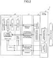
- FIG. 2 is a block diagram illustrating a function of a main part of the endoscope system 1. Referring to FIG. 2 , a detail of each configuration of the endoscope system 1 and a path of an electric signal inside the endoscope system 1 will be described.
- the imaging unit 20 includes a first chip 21 (an image sensor) and a second chip 22.
- the first chip 21 includes a light receiving unit 23 in which a plurality of unit pixels are arranged in a matrix direction to have a two-dimensional matrix shape, a reading unit 24 which reads an imaging signal photoelectrically converted by the light receiving unit 23, a timing generating unit 25 which generates a timing signal based on a reference clock signal and a synchronization signal input from the connector part 5 and outputs the timing signal to the reading unit 24, and a buffer 26 which amplifies the imaging signal and the reference signal read from the light receiving unit 23 by the reading unit 24.
- a more detailed configuration of the first chip 21 will be described with reference to FIG. 3 .
- the second chip 22 includes a buffer 27 which serves as a transfer unit for transmitting the imaging signal output from the first chip 21 to the processor 6 via the transfer cable 3 and the connector part 5.
- a combination of circuits mounted on the first chip 21 and the second chip 22 can be appropriately changed in accordance with the setting.
- the imaging unit 20 receives a power supply voltage VDD which is generated by a power supply unit 61 inside the processor 6 via the transfer cable 3 together with a ground GND.
- a power stabilizing condenser C100 is provided between the ground GND and the power supply voltage VDD supplied to the imaging unit 20.
- the connector part 5 includes an analog front end unit 51 (hereinafter, referred to as an "AFE unit 51") and an imaging signal processing unit 52.
- the connector part 5 serves as a relay processing part which electrically connects the endoscope 2 (the imaging unit 20) to the processor 6 and relays an electric signal.
- the connector part 5 and the imaging unit 20 are connected to each other via the transfer cable 3 and the connector part 5 and the processor 6 are connected to each other via a coil cable. Further, the connector part 5 is also connected to the light source device 8.
- the AFE unit 51 receives an imaging signal transferred from the imaging unit 20, performs impedance matching using a passive element such as a resistor, extracts an AC component by a condenser, and determines an operation point by a voltage dividing resistor.
- the AFE unit 51 performs A/D converting on an analog imaging signal transferred from the imaging unit 20 and outputs a digital imaging signal to the imaging signal processing unit 52.
- the imaging signal processing unit 52 performs a predetermined signal process such as vertical line removal and noise removal on the digital imaging signal input from the AFE unit 51 and outputs a result to the processor 6.
- the imaging signal processing unit 52 is configured by using, for example, a Field Programmable Gate Array (FPGA). Further, the imaging signal processing unit 52 generates a synchronization signal representing a start position of each frame based on a reference clock signal (for example, a clock signal of 27 MHz) supplied from the processor 6 and corresponding to a reference of an operation of each elements of the endoscope 2 and outputs the synchronization signal to the timing generating unit 25 of the imaging unit 20 via the transfer cable 3 along with the reference clock signal.
- the synchronization signal includes a horizontal synchronization signal and a vertical synchronization signal.
- the processor 6 is a control device which generally controls the entire endoscope system 1.
- the processor 6 includes a power supply unit 61 and an image signal processing unit 62.
- the power supply unit 61 generates a power supply voltage VDD and supplies the generated power supply voltage to the imaging unit 20 via the connector part 5 and the transfer cable 3 along with the ground GND.
- the image signal processing unit 62 performs an image process such as a synchronization process, a white balance (WB) adjustment process, a gain adjustment process, a gamma correction process, a digital/analog (for example, D/A) conversion process, and a format conversion process on the digital imaging signal having been subjected to the signal process by the imaging signal processing unit 52 to convert the imaging signal into an image signal and outputs the image signal to the display device 7.
- WB white balance
- WB white balance
- gain adjustment process e.g., a gain adjustment process
- a gamma correction process e.g., a digital/analog (for example, D/A) conversion process
- the display device 7 displays an image captured by the imaging unit 20 based on the image signal input from the image signal processing unit 62.
- the display device 7 is configured by using a display panel such as a liquid crystal or an organic Electro Luminescence (EL).
- a display panel such as a liquid crystal or an organic Electro Luminescence (EL).
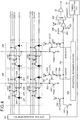
- FIG. 3 is a block diagram illustrating a detailed configuration of the first chip 21 illustrated in FIG. 2 .
- FIG. 4 is a circuit diagram illustrating a configuration of the first chip 21.
- the first chip 21 includes the light receiving unit 23, the reading unit 24 (the driving unit), the timing generating unit 25, the buffer 26, and a hysteresis circuit 28.
- the hysteresis circuit 28 performs waveform shaping on the reference clock signal and the synchronization signal input via the transfer cable 3 and outputs the reference clock signal and the synchronization signal having been subjected to the waveform shaping to the timing generating unit 25.
- the timing generating unit 25 generates various drive signals ( ⁇ Ta, ⁇ Tb, ⁇ R, ⁇ X, ⁇ VCL, ⁇ HCLR, ⁇ HCLK, ⁇ MUXSEL, ⁇ HSH) based on the reference clock signal and the synchronization signal shaped by the hysteresis circuit 28 and supplies the drive signals to a vertical scanning portion 241, a noise removing portion 243, a horizontal scanning portion 245, a multiplexer 260 (hereinafter, referred to as a "MUX 260”), and a reference voltage generating portion 246.
- MUX 260 multiplexer 260
- the reading unit 24 includes the vertical scanning portion 241 (the row selection circuit), a constant current source 242, the noise removing portion 243, a column source follower transistor 244 (a first transistor), a horizontal scanning portion 245 (a column selection circuit), and a reference voltage generating portion 246.
- the noise removing portion 243 removes an output variation and a pixel resetting noise signal of each unit pixel 230 and outputs an imaging signal photoelectrically converted by each unit pixel 230 to the column source follower transistor 244. In addition, a detail of the noise removing portion 243 will be described with reference to FIG. 4 .
- the multiplexer 260 is driven by the drive signal ( ⁇ MUXSEL) supplied from the timing generating unit 25 and alternatively outputs the imaging signal input via the horizontal transfer line 258 and the reference voltage Vref (the constant voltage signal) generated by the reference voltage generating portion 246 to the buffer 26.
- the output reference voltage Vref is used in the imaging signal processing unit 52 and the like of the connector part 5 to remove the same-phase superimposed noise by the transfer cable 3 during the transfer of the imaging signal.
- an amplifier for adjusting a gain may be provided at the input side of the multiplexer 260.
- the buffer 26 amplifies the noise removed imaging signal and the reference voltage Vref (the constant voltage signal) if necessary and alternately outputs the noise removed imaging signal and the reference voltage Vref to the second chip 22.
- the plurality of unit pixels 230 are arranged in a two-dimensional matrix shape in the light receiving unit 23 of the first chip 21.
- Each unit pixel 230 includes a photoelectric conversion element 231 (a photodiode), a photoelectric conversion element 232, a charge conversion portion 233, a transfer transistor 234 (a first transfer portion), a transfer transistor 235, a charge conversion portion resetting portion 236 (a transistor), a pixel source follower transistor 237, and a pixel output switch 238 (a signal output portion).
- a photoelectric conversion element 231 a photodiode
- a photoelectric conversion element 232 a charge conversion portion 233
- a transfer transistor 234 a first transfer portion
- a transfer transistor 235 a charge conversion portion resetting portion 236
- a pixel source follower transistor 237 a pixel source follower transistor 237
- a pixel output switch 238 a signal output portion
- the photoelectric conversion element 231 and the photoelectric conversion element 232 photoelectrically convert the incident light into a signal charge amount in response to the light amount and store the signal charge amount.
- Cathodes of the photoelectric conversion element 231 and the photoelectric conversion element 232 are respectively connected to one ends of the transfer transistor 234 and the transfer transistor 235 and anodes thereof are connected to the ground GND.
- the charge conversion portion 233 is configured as a floating diffusion capacity (FD) and converts a charge stored by the photoelectric conversion element 231 and the photoelectric conversion element 232 into a voltage.
- FD floating diffusion capacity
- the transfer transistor 234 and the transfer transistor 235 respectively transfer charges from the photoelectric conversion element 231 and the photoelectric conversion element 232 to the charge conversion portion 233.
- Signal lines to which row selection signals (row selection pulses) ⁇ Ta and ⁇ Tb are supplied are respectively connected to the gates of the transfer transistor 234 and the transfer transistor 235 and the charge conversion portion 233 is connected to the other end thereof.
- the transfer transistor 234 and the transfer transistor 235 are turned on when the row selection signals ⁇ Ta and ⁇ Tb are supplied from the vertical scanning portion 241 thereto via the signal line, signal charges are transferred from the photoelectric conversion element 231 and the photoelectric conversion element 232 to the charge conversion portion 233.
- the charge conversion portion resetting portion 236 resets the charge conversion portion 233 to a predetermined potential.
- One end of the charge conversion portion resetting portion 236 is connected to the power supply voltage VDD, the other end thereof is connected to the charge conversion portion 233, and a gate thereof is connected to a signal line to which the row selection signal ⁇ R is supplied.
- the charge conversion portion resetting portion 236 is turned on when the row selection signal ⁇ R is supplied from the vertical scanning portion 241 thereto via the signal line and discharges the signal charge stored in the charge conversion portion 233 so that the charge conversion portion 233 is reset to a predetermined potential.
- One end of the pixel source follower transistor 237 is connected to the power supply voltage VDD, the other end thereof is connected to one end of the pixel output switch 238, and a gate thereof receives a signal (an image signal or a resetting signal) converted into a voltage by the charge conversion portion 233.
- the pixel output switch 238 outputs a signal which is converted into a voltage by the charge conversion portion 233 to the vertical transfer line 239.
- the other end of the pixel output switch 238 is connected to the vertical transfer line 239 and a gate thereof is connected to a signal line to which the row selection signal ⁇ X is supplied.
- the pixel output switch 238 is turned on when the row selection signal ⁇ X is supplied from the vertical scanning portion 241 to the gate of the pixel output switch 238 via the signal line and transfers the image signal or the resetting signal to the vertical transfer line 239.
- the vertical transfer line 239 is provided for each vertical line of the unit pixel 230 and transfers the imaging signal output from the unit pixel 230.
- the constant current source 242 is provided in each of the vertical transfer lines 239. One end of the constant current source 242 is connected to the vertical transfer line 239, the other end thereof is connected to the ground GND, and a gate thereof receives a bias voltage Vbias1.
- the constant current source 242 drives the unit pixel 230 and reads the output of the unit pixel 230 to the vertical transfer line 239. A signal which is read to the vertical transfer line 239 is input to the noise removing portion 243.
- the noise removing portion 243 includes a transfer capacity 252 (a capacitor) and a clamp switch 253 (a second transistor).
- One end of the transfer capacity 252 is connected to the vertical transfer line 239 and the other end thereof is connected to the column source follower transistor 244.
- One end of the clamp switch 253 is connected to a signal line to which a clamp voltage Vclp is supplied from the reference voltage generating portion 246, the other end thereof is connected between the transfer capacity 252 and the column source follower transistor 244, and a gate thereof receives the drive signal ⁇ VCL from the timing generating unit 25.
- An imaging signal which is input to the noise removing portion 243 is an optical noise signal including a noise component.
- the clamp switch 253 When the drive signal ⁇ VCL is input from the timing generating unit 25 to the gate of the clamp switch 253, the clamp switch 253 is turned on so that the transfer capacity 252 is reset by the clamp voltage Vclp supplied from the reference voltage generating portion 246.
- the imaging signal having been subjected to noise removal by the noise removing portion 243 is input to the gate of the column source follower transistor 244.
- the noise removing portion 243 does not need a sampling condenser (a sampling capacity)
- the capacity of the transfer capacity 252 may be sufficiently larger than the input capacity of the column source follower transistor 244.
- One end of the column source follower transistor 244 is connected to the power supply voltage VDD, the other end thereof is connected to one end of a column selection switch 254 (the third transistor), and a gate thereof receives an imaging signal having been subjected to noise removal by the noise removing portion 243.
- the column source follower transistor 244 (the first transistor) and the clamp switch 253 (the second transistor) serve as a column reading circuit.
- One end of the column selection switch 254 is connected to the other end of the column source follower transistor 244, the other end thereof is connected to the horizontal transfer line 258 (the second transfer line), and a gate thereof is connected to a signal line which supplies the column selection signal ⁇ HCLK ⁇ M> from the horizontal scanning portion 245.
- the column selection switch 254 is turned on when the column selection signal ⁇ HCLK ⁇ M> is supplied from the horizontal scanning portion 245 to the gate of the column selection switch 254 of the column ⁇ M> and transfers a signal of the vertical transfer line 239 of the column ⁇ M> (an imaging signal having been subjected to noise removal of the noise removing portion 243) to the horizontal transfer line 258.
- the column selection switch 254 serves as a column scanning circuit.
- One end of a horizontal reset transistor 256 is connected to the ground GND, the other end thereof is connected to the horizontal transfer line 258, and a gate thereof receives the drive signal ⁇ HCLR from the timing generating unit 25.
- the horizontal reset transistor 256 is turned on when the drive signal ⁇ HCLR is input from the timing generating unit 25 to the gate of the horizontal reset transistor 256 and resets the horizontal transfer line 258.
- a constant current source 257 is connected to the horizontal transfer line 258, the other end thereof is connected to the ground GND, and a gate thereof receives a bias voltage Vbias2.
- the constant current source 257 reads an imaging signal from the vertical transfer line 239 to the horizontal transfer line 258.
- the imaging signal which is read to the horizontal transfer line 258 is input to a sample hold portion 255.
- the horizontal transfer line 258 is connected to each of the column selection switches 254 and transfers an imaging signal via the column source follower transistor 244.
- the sample hold portion 255 includes a sample hold switch 262 (a transistor), a sample capacity (a condenser) 263, and an op amp 264.
- One end of the sample hold switch 262 is connected to the horizontal transfer line 258, the other end thereof is connected to the input of the op amp 264, and an imaging signal and a horizontal resetting noise signal are input thereto via the horizontal transfer line 258.
- One end of the sample capacity 263 is connected to the other end of the sample hold switch 262 and the input of the op amp 264 and the other end thereof is connected to the ground GND.
- the output of the op amp 264 is connected to the inverting input terminal of the op amp 264 and the input of the multiplexer 260.
- the sample hold portion 255 holds a voltage immediately before the sample hold switch 262 is turned off by the sample capacity 263 and outputs a voltage held by the sample capacity 263 while the sample hold switch 262 is turned off.
- the first embodiment it is possible to suppress the crosstalk of the imaging signal in the column direction by alternatively performing the resetting of the horizontal transfer line 258 using the horizontal reset transistor 256 and the reading of the imaging signal having been subjected to noise removal from the vertical transfer line 239. Further, when the sample hold switch 262 of the sample hold portion 255 is turned on during the transfer of the imaging signal having been subjected to the noise removal and is turned off during the transfer of the resetting noise signal, only the imaging signal having been subjected to noise removal can be output to the op amp 264. Since the first chip 21 includes the sample hold portion 255, the band of the amplifier circuit in the subsequent stage can be halved and the range thereof can be suppressed.
- the multiplexer 260 alternatively outputs the noise removed imaging signal output from the sample hold portion 255 and the reference voltage Vref generated by the reference voltage generating portion 246 to the second chip 22.
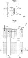
- FIG. 5 is a circuit diagram illustrating a configuration of the reference voltage generating portion 246 of the light receiving unit 23 of the endoscope system 1 according to the first embodiment.
- the reference voltage generating portion 246 (the constant voltage signal generating portion) includes a resistance voltage dividing circuit which includes two resistors 291 and 292 and a sampling capacity 294 (a condenser) which releases fluctuation independently from the power supply and the switch 293 (the transistor) driven by the drive signal ⁇ VSH.
- the reference voltage generating portion 246 generates the clamp voltage Vclp of the noise removing portion 243 and the reference voltage Vref (the constant voltage signal) from the same power supply voltage VDD as that of the light receiving unit 23 at a timing in which the drive signal ⁇ VSH is driven by the driving of the switch 293.
- the reference voltage Vref and the clamp voltage Vclp are generated at the same timing from the same power supply, the reference voltage Vref reflects an influence of the power fluctuation for the imaging signal output from the noise removing portion 243. Further, the reference voltage Vref reflects the transfer noise information during transfer in the transfer cable 3. Thus, it is possible to obtain the imaging signal from which noise is removed during transfer by performing a noise removal process such as a correlated double sampling on the connector part 5 in such a manner that the noise removed imaging signal and the reference voltage Vref are alternatively transferred to the connector part 5.
- FIG. 6 is a top view of the first chip 21 including at least the column source follower transistor 244, the transfer capacity 252, the clamp switch 253, and the column selection switch 254.
- FIG. 7 is a cross-sectional view obtained by cutting the first chip 21 at a position including at least the transfer capacity 252.
- the transfer capacity 252 (the capacitor) has a trench structure including a first electrode 252a formed on a first diffusion layer 30. Further, the transfer capacity 252 includes a trench 252b which is formed in the first diffusion layer 30 and a dielectric film 252c which is formed inside the trench 252b.
- the dielectric film 252c is formed of SiO 2 (silicon oxide), Si 3 N 4 (silicon nitride), Al 2 O 3 (aluminum oxide), HfO 2 (hafnium oxide), ZrO 2 (zirconium oxide), Ta 2 O 5 (tantalum oxide), TiO 2 (titanium oxide), Y 2 O 3 (yttrium oxide), and La 2 O 3 (lanthanum oxide).
- the first electrode 252a is formed at the inside of the dielectric film 252c in the transfer capacity 252. Further, the vertical transfer line 239 is connected to the first diffusion layer 30. Accordingly, the imaging signal from the pixel output switch 238 is transferred to the first diffusion layer 30.
- a gate of the column source follower transistor 244 (the first transistor) is connected to the first electrode 252a via the trench 252b, a drain thereof is connected to the power supply voltage VDD, and a source thereof is connected to the column selection switch 254 (the third transistor).
- the column source follower transistor 244 amplifies the imaging signal output from the pixel output switch 238 via the vertical transfer line 239 and outputs the imaging signal to the horizontal transfer line 258 via the column selection switch 254.
- a source of the clamp switch 253 (the second transistor) is connected to the first electrode 252a via the trench 252b and a drain thereof is connected to a signal line from which the clamp voltage Vclp is supplied from the reference voltage generating portion 246.
- the clamp switch 253 is turned on when the drive signal ⁇ VCL is input thereto from the timing generating unit 25, resets the potential of the first electrode 252a inside the trench 252b to the clamp voltage Vclp supplied from the reference voltage generating portion 246, and transfers only the imaging signal output from the pixel output switch 238 via the vertical transfer line 239 to the column source follower transistor 244.
- the column selection switch 254 (the third transistor) is connected to the vertical transfer line 239 via the transfer capacity 252 and outputs the imaging signal from the vertical transfer line 239 to the horizontal transfer line 258 via the column source follower transistor 244.
- each of the column reading circuit including the column source follower transistor 244 and the clamp switch 253 is separated by a second diffusion layer 31.
- FIG. 8 is a cross-sectional view of a first chip obtained by cutting at a position including a transfer capacity of a first modified example of the first embodiment of the invention.
- the same reference numerals will be given to the same elements as those of the endoscope system 1 according to the above-described first embodiment and the description thereof will be omitted.
- a first chip 21b includes a first electrode 252d and a second electrode 252e instead of the first electrode 252a connected to the vertical transfer line 239 of the transfer capacity 252 according to the above-described first embodiment.
- the second electrode 252e is formed by using an impurity-doped polysilicon and is formed to be embedded in the trench 252b.
- the dielectric film 252c is formed inside the second electrode 252e.
- the first electrode 252d is formed inside the dielectric film 252c.
- the first electrode 252d is formed at a position facing the second electrode 252e with the dielectric film 252c interposed therebetween.
- the first diffusion layer 30 is connected to each of the second electrode 252e and the vertical transfer line 239.
- the dielectric film 252c and the first electrode 252d are formed after the second electrode 252e is provided in the trench 252b formed on the second diffusion layer 31, it is possible to form a deep trench 252b without using a high-energy ion implanter.
- FIG. 9 is a cross-sectional view of a first chip obtained by cutting at a position including the transfer capacity of the second modified example of the first embodiment of the invention. Additionally, in the second modified example of the first embodiment, the same reference numerals will be given to the same elements as those of the endoscope system 1 according to the above-described first embodiment and the description thereof will be omitted.
- a first chip 21c illustrated in FIG. 9 includes a separation member 32 that separates the first diffusion layer 30 and the second diffusion layer 31 from each other.
- the first chip 21c is formed by using a Silicon On Insulator (SOI) substrate including a layer of a silicon oxide film, a deep trench deeper than the trench 252b is formed in the second diffusion layer 31, and the separation member 32 formed as a silicon oxide film is injected thereinto, thereby separating the first diffusion layer 30 and the second diffusion layer 31 from each other.
- SOI Silicon On Insulator
- the capacity of the column source follower transistor 244 can be decreased.
- a configuration of a first chip is different from a configuration of the first chip 21 according to the above-described first embodiment.
- a stacked imager chip will be used as the first chip according to the second embodiment.
- a configuration of the first chip according to the second embodiment will be described here below.
- the same reference numerals will be given to the same elements as those of the endoscope system 1 according to the above-described first embodiment and the description thereof will be omitted.
- FIG. 10 is a top view including a column source follower transistor, a transfer capacity, a clamp switch, and a column selection switch of a first chip according to the second embodiment of the invention.
- FIG. 11 is a cross-sectional view obtained by cutting the first chip at a position including the transfer capacity according to the second embodiment of the invention. Additionally, the configurations of the unit pixel 230 and the like are omitted in FIGS. 10 and 11 in order to simplify the description.
- a first chip 21d illustrated in FIGS. 10 and 11 is configured by using a front side illumination imager chip.
- the first chip 21d includes a pixel chip 40, a circuit chip 41, a connection portion 42 (a bump) which electrically connects the pixel chip 40 and the circuit chip 41 to each other, and a first electrode 43 which is provided between the connection portion 42 and the circuit chip 41.
- the first chip 21d is formed by sequentially stacking the circuit chip 41, the first electrode 43, the connection portion 42, and the pixel chip 40.
- the circuit chip 41 is provided with the column source follower transistor 244, the clamp switch 253, and the column selection switch 254.
- the first electrode 43 is provided to be stacked on the column source follower transistor 244, a lower end thereof is connected to the column source follower transistor 244, and an upper end thereof is connected to the connection portion.
- connection portion 42 is provided to be stacked on the first electrode 43, a lower end thereof is connected to the first electrode 43, and an upper end thereof is connected to the pixel chip 40.
- the connection portion 42 is formed by using, for example, gold or the like.
- the pixel chip 40 is provided with the vertical transfer line 239 and the transfer capacity 252. Additionally, the pixel chip 40 is provided with the unit pixel 230 (not illustrated).
- the transfer capacity 252 includes the trench 252b which is formed in the first diffusion layer 30, the dielectric film 252c which is formed inside the trench 252b, an electrode 252f which is formed inside the dielectric film 252c, and the second diffusion layer 31 which separates the first diffusion layer 30. Further, the first diffusion layer 30 is connected to the vertical transfer line 239.
- circuits such as the column source follower transistor 244, the clamp switch 253, and the column selection switch 254 are disposed on the circuit chip 41 different from the pixel chip 40, it is possible to realize further miniaturization compared to the above-described first embodiment.
- a plurality of transfer capacities may be provided inside the pixel chip. Accordingly, it is possible to obtain the imaging signal with higher image quality.
- a back side illumination imager chip will be used as the first chip.
- a configuration of the first chip according to the third embodiment will be described here below.
- the same reference numerals will be given to the same elements as those of the endoscope system 1 according to the above-described first embodiment and the description thereof will be omitted.
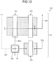
- FIG. 12 is a top view of a circuit chip of a first chip according to the third embodiment of the invention.
- FIG. 13 is a cross-sectional view obtained by cutting at a position including the transfer capacity of the first chip according to the third embodiment of the invention.
- the configurations of the unit pixel 230 and the like are omitted in order to simplify the description in FIGS. 12 and 13 .
- a first chip 21e illustrated in FIGS. 12 and 13 is configured by using a back side illumination imager chip.
- the first chip 21e includes a pixel chip 40a, a circuit chip 41a, and a connection portion 42 (a bump) which electrically connects the pixel chip 40a and the circuit chip 41a to each other.
- the first chip 21e is formed by sequentially stacking the pixel chip 40a, the connection portion 42, and the circuit chip 41a.
- the pixel chip 40a is provided with the vertical transfer line 239 and the transfer capacity 252.
- the pixel chip 40a is provided with the unit pixel 230 (not illustrated).
- the transfer capacity 252 includes the trench 252b which is formed in the first diffusion layer 30, the dielectric film 252c which is formed inside the trench 252b, the first electrode 252a which is formed inside the dielectric film, and the second diffusion layer 31 which separates the first diffusion layer 30. Further, the first diffusion layer 30 is connected to the vertical transfer line 239.
- connection portion 42 is provided to be stacked on the first electrode 252a, a lower end thereof is connected to the first electrode 252a, and an upper end thereof is connected to the circuit chip 41a.
- the connection portion 42 is formed by using, for example, gold or the like.
- the circuit chip 41a is provided with the column source follower transistor 244, the clamp switch 253, and the column selection switch 254.
- circuits such as the column source follower transistor 244, the clamp switch 253, and the column selection switch 254 are disposed on the circuit chip 41a different from the pixel chip 40a, it is possible to realize further miniaturization compared to the above-described first embodiment.
Landscapes
- Engineering & Computer Science (AREA)
- Physics & Mathematics (AREA)
- Health & Medical Sciences (AREA)
- Life Sciences & Earth Sciences (AREA)
- Multimedia (AREA)
- Signal Processing (AREA)
- Surgery (AREA)
- Optics & Photonics (AREA)
- Biomedical Technology (AREA)
- General Health & Medical Sciences (AREA)
- Radiology & Medical Imaging (AREA)
- Nuclear Medicine, Radiotherapy & Molecular Imaging (AREA)
- Biophysics (AREA)
- Heart & Thoracic Surgery (AREA)
- Medical Informatics (AREA)
- Molecular Biology (AREA)
- Animal Behavior & Ethology (AREA)
- Pathology (AREA)
- Public Health (AREA)
- Veterinary Medicine (AREA)
- Astronomy & Astrophysics (AREA)
- General Physics & Mathematics (AREA)
- Solid State Image Pick-Up Elements (AREA)
- Transforming Light Signals Into Electric Signals (AREA)
- Instruments For Viewing The Inside Of Hollow Bodies (AREA)
- Endoscopes (AREA)
Abstract
Description
- The present invention relates to an image sensor that generates image data of an object by capturing an image of the object.
- Hitherto, a technique is known in which only a transfer capacity for transferring an imaging signal is provided in a noise removing portion disposed in each of pixel columns in order to remove a reset noise of a charge voltage converting portion inside a unit pixel in a Complementary Metal Oxide Semiconductor (CMOS) image sensor (see Patent Literature 1). According to this technique, it is possible to realize a compatibility between further miniaturization and high image quality of the image sensor by decreasing an area occupied by the noise removing portion while suppressing the capacity of the transfer capacity to be low without providing a sampling condenser inside the noise removing portion in terms of a noise signal reading operation of resetting the transfer capacity after resetting the pixel and outputting a signal of the pixel and an optical noise signal reading operation of outputting a signal of the pixel after transferring a charge stored in the pixel.
- Patent Literature 1:
JP 5596888 B1 - Incidentally, there has been a demand for further miniaturizing the image sensor in general. In order to meet this demand, a case of decreasing the area occupied by the noise removing portion in accordance with a decrease in capacity of the transfer capacity is considered in the case of
Patent Literature 1. However, when the capacity of the transfer capacity is further decreased, there are problems in which noise of the image signal cannot be sufficiently removed and high image quality cannot be obtained. - The invention has been made in view of the above-described circumstances and an object of the invention is to provide an image sensor capable of realizing a compatibility between further miniaturization and high image quality.
- To solve the problem described above and to achieve the object, an image sensor according to the present invention includes: a plurality of pixels arranged in a two-dimensional matrix shape, each pixel being configured to receive external light, generate an imaging signal in response to a light receiving amount and output the generated imaging signal; a plurality of first transfer lines configured to transfer the imaging signal output from each of the pixels, each first transfer line being provided for each vertical line in an arrangement of the pixels; a plurality of capacitors, each capacitor being provided at a respective one of the first transfer lines and having a trench structure including a first electrode formed on a first diffusion layer; a plurality of column reading circuits, each column reading circuit including: a first transistor including a gate connected to the first electrode, the first transistor being configured to amplify the imaging signal; and a second transistor including a source connected to the first electrode, the second transistor being configured to reset the capacitor to a predetermined potential, each column reading circuit being provided at a respective one of the first transfer lines and separated from the capacitor by a second diffusion layer; a plurality of column scanning circuits, each column scanning circuit including a third transistor connected to the first transfer line via the capacitor and configured to output the imaging signal from the first transfer line via the first transistor, each column scanning circuit being provided at a respective one of the column reading circuits; a second transfer line connected to the third transistor and configured to transfer the imaging signal via the first transistor; and a constant current source connected to the second transfer line and configured to output the imaging signal from each of the first transfer lines to the second transfer line.
- In the image sensor according to the present invention, the capacitor includes a trench which is formed in the first diffusion layer and a dielectric film which is formed inside the trench. The first electrode is provided inside the dielectric film. The first transfer line is connected to the first diffusion layer.
- In the image sensor according to the present invention, the capacitor includes a trench which is formed in the second diffusion layer, a second electrode which is formed inside the trench, and a dielectric film which is formed inside the second electrode. The first electrode is provided inside the dielectric film and is provided at a position facing the second electrode with the dielectric film interposed therebetween. The first diffusion layer is connected to each of the second electrode and the first transfer line.
- The image sensor according to the present invention further includes a separation member configured to separate the first diffusion layer and the second diffusion layer from each other.
- The image sensor according to the present invention includes: a circuit chip which is provided with the column reading circuits, the column scanning circuits, the second transfer line, and the constant current source; a pixel chip which is stacked on the circuit chip and is provided with the pixels, the first transfer lines, and the capacitors; and a connection portion configured to connect the first electrode and the first transistor to each other. The capacitor includes a trench which is formed in the first diffusion layer and a dielectric film which is formed inside the trench. The first electrode is provided inside the dielectric film and is connected to the first transfer line.
- The image sensor according to the present invention includes: a pixel chip which is provided with the pixels, the first transfer lines, and the capacitors; a circuit chip which is stacked on the pixel chip and is provided with the column reading circuits, the column scanning circuits, the second transfer line, and the constant current source; and a connection portion configured to connect the first electrode and the first transistor to each other. The capacitor includes a trench which is formed in the first diffusion layer and a dielectric film which is formed inside the trench. The first electrode is formed inside the dielectric film. The first transfer line is connected to the first diffusion layer.
- According to the image sensor of the invention, it is possible to realize compatibility between further miniaturization and high image quality.
-
-
FIG. 1 is a diagram schematically illustrating an overall configuration of an endoscope system according to a first embodiment of the invention. -
FIG. 2 is a block diagram illustrating a function of a main part of the endoscope system according to the first embodiment of the invention. -
FIG. 3 is a block diagram illustrating a detailed configuration of a first chip illustrated inFIG. 2 . -
FIG. 4 is a circuit diagram illustrating a configuration of the first chip. -
FIG. 5 is a circuit diagram illustrating a configuration of a reference voltage generating portion of a light receiving unit of the endoscope system according to the first embodiment of the invention. -
FIG. 6 is a top view of a first chip including at least a column source follower transistor, a transfer capacity, a clamp switch, and a column selection switch. -
FIG. 7 is a cross-sectional view obtained by cutting a first chip at a position including at least a transfer capacity. -
FIG. 8 is a cross-sectional view obtained by cutting a first chip at a position including a transfer capacity of a first modified example of the first embodiment of the invention. -
FIG. 9 is a cross-sectional view obtained by cutting a first chip at a position including a transfer capacity of a second modified example of the first embodiment of the invention. -
FIG. 10 is a top view including a column source follower transistor, a transfer capacity, a clamp switch, and a column selection switch of a first chip according to a second embodiment of the invention. -
FIG. 11 is a cross-sectional view obtained by cutting a first chip at a position including a transfer capacity according to the second embodiment of the invention. -
FIG. 12 is a top view of a circuit chip in a first chip according to a third embodiment of the invention. -
FIG. 13 is a cross-sectional view obtained by cutting at a position including a transfer capacity in the first chip according to the third embodiment of the invention. Description of Embodiments - Hereinafter, an endoscope system including an imaging device will be described as a mode for carrying out the invention (hereinafter referred to as an "embodiment"). Further, the invention is not limited by the embodiment. Further, in the description of the drawings, the same parts will be described by the same reference numerals. Furthermore, it should be noted that the drawings are schematic and the relation between the thickness and the width of each member, the scale of each member, and the like are different from the reality. Also, parts having different dimensions and scales are included in the drawings.
-
FIG. 1 is a diagram schematically illustrating an overall configuration of an endoscope system according to a first embodiment of the invention. Anendoscope system 1 illustrated inFIG. 1 includes an endoscope 2, atransfer cable 3, aconnector part 5, a processor 6 (a processing device), adisplay device 7, and a light source device 8. - The endoscope 2 captures an in-vivo image of a subject by inserting an
insertion part 100 which is a part of thetransfer cable 3 into a body cavity of the subject and outputs an image signal (image data) to theprocessor 6. Further, the endoscope 2 has a configuration in which an imaging unit 20 (an imaging device) for capturing an in-vivo image is provided at a position corresponding to one end side of thetransfer cable 3 and corresponding to adistal end 101 of theinsertion part 100 inserted into the body cavity of the subject and anoperation part 4 for receiving various operations of the endoscope 2 is connected to aproximal end 102 of theinsertion part 100. Theimaging unit 20 is connected to theconnector part 5 through theoperation part 4 by thetransfer cable 3. An image signal of an image which is captured by theimaging unit 20 is output to theconnector part 5, for example, along thetransfer cable 3 having a length of several meters. - The
connector part 5 is connected to the endoscope 2, theprocessor 6, and the light source device 8 and performs a predetermined signal process on an image signal output from the connected endoscope 2 and a conversion (an A/D conversion) of converting an imaging signal from an analog signal into a digital signal so that the image signal is output to theprocessor 6. - The
processor 6 includes a CPU (Central Processing Unit) and the like and is used to perform a predetermined image process on an image signal output from theconnector part 5 and controls theentire endoscope system 1. Further, in the first embodiment, theprocessor 6 serves as a processing device. - The
display device 7 displays an image corresponding to an image signal having been subjected to an image process of theprocessor 6. Further, thedisplay device 7 displays various information on theendoscope system 1. - The light source device 8 includes, for example an xenon lamp or a white LED (Light Emitting Diode) and emits illumination light toward a subject from the
distal end 101 of theinsertion part 100 of the endoscope 2 via theconnector part 5 and thetransfer cable 3. -
FIG. 2 is a block diagram illustrating a function of a main part of theendoscope system 1. Referring toFIG. 2 , a detail of each configuration of theendoscope system 1 and a path of an electric signal inside theendoscope system 1 will be described. - As illustrated in
FIG. 2 , theimaging unit 20 includes a first chip 21 (an image sensor) and asecond chip 22. - The
first chip 21 includes alight receiving unit 23 in which a plurality of unit pixels are arranged in a matrix direction to have a two-dimensional matrix shape, areading unit 24 which reads an imaging signal photoelectrically converted by thelight receiving unit 23, atiming generating unit 25 which generates a timing signal based on a reference clock signal and a synchronization signal input from theconnector part 5 and outputs the timing signal to thereading unit 24, and abuffer 26 which amplifies the imaging signal and the reference signal read from thelight receiving unit 23 by thereading unit 24. In addition, a more detailed configuration of thefirst chip 21 will be described with reference toFIG. 3 . - The
second chip 22 includes abuffer 27 which serves as a transfer unit for transmitting the imaging signal output from thefirst chip 21 to theprocessor 6 via thetransfer cable 3 and theconnector part 5. In addition, a combination of circuits mounted on thefirst chip 21 and thesecond chip 22 can be appropriately changed in accordance with the setting. - Further, the
imaging unit 20 receives a power supply voltage VDD which is generated by a power supply unit 61 inside theprocessor 6 via thetransfer cable 3 together with a ground GND. A power stabilizing condenser C100 is provided between the ground GND and the power supply voltage VDD supplied to theimaging unit 20. - The
connector part 5 includes an analog front end unit 51 (hereinafter, referred to as an "AFE unit 51") and an imagingsignal processing unit 52. Theconnector part 5 serves as a relay processing part which electrically connects the endoscope 2 (the imaging unit 20) to theprocessor 6 and relays an electric signal. Theconnector part 5 and theimaging unit 20 are connected to each other via thetransfer cable 3 and theconnector part 5 and theprocessor 6 are connected to each other via a coil cable. Further, theconnector part 5 is also connected to the light source device 8. - The
AFE unit 51 receives an imaging signal transferred from theimaging unit 20, performs impedance matching using a passive element such as a resistor, extracts an AC component by a condenser, and determines an operation point by a voltage dividing resistor. TheAFE unit 51 performs A/D converting on an analog imaging signal transferred from theimaging unit 20 and outputs a digital imaging signal to the imagingsignal processing unit 52. - The imaging
signal processing unit 52 performs a predetermined signal process such as vertical line removal and noise removal on the digital imaging signal input from theAFE unit 51 and outputs a result to theprocessor 6. The imagingsignal processing unit 52 is configured by using, for example, a Field Programmable Gate Array (FPGA). Further, the imagingsignal processing unit 52 generates a synchronization signal representing a start position of each frame based on a reference clock signal (for example, a clock signal of 27 MHz) supplied from theprocessor 6 and corresponding to a reference of an operation of each elements of the endoscope 2 and outputs the synchronization signal to thetiming generating unit 25 of theimaging unit 20 via thetransfer cable 3 along with the reference clock signal. Here, the synchronization signal includes a horizontal synchronization signal and a vertical synchronization signal. - The
processor 6 is a control device which generally controls theentire endoscope system 1. Theprocessor 6 includes a power supply unit 61 and an imagesignal processing unit 62. - The power supply unit 61 generates a power supply voltage VDD and supplies the generated power supply voltage to the
imaging unit 20 via theconnector part 5 and thetransfer cable 3 along with the ground GND. - The image
signal processing unit 62 performs an image process such as a synchronization process, a white balance (WB) adjustment process, a gain adjustment process, a gamma correction process, a digital/analog (for example, D/A) conversion process, and a format conversion process on the digital imaging signal having been subjected to the signal process by the imagingsignal processing unit 52 to convert the imaging signal into an image signal and outputs the image signal to thedisplay device 7. - The
display device 7 displays an image captured by theimaging unit 20 based on the image signal input from the imagesignal processing unit 62. Thedisplay device 7 is configured by using a display panel such as a liquid crystal or an organic Electro Luminescence (EL). - Next, a detailed configuration of the
first chip 21 will be described.FIG. 3 is a block diagram illustrating a detailed configuration of thefirst chip 21 illustrated inFIG. 2 .FIG. 4 is a circuit diagram illustrating a configuration of thefirst chip 21. - As illustrated in
FIGS. 3 and4 , thefirst chip 21 includes thelight receiving unit 23, the reading unit 24 (the driving unit), thetiming generating unit 25, thebuffer 26, and ahysteresis circuit 28. - The
hysteresis circuit 28 performs waveform shaping on the reference clock signal and the synchronization signal input via thetransfer cable 3 and outputs the reference clock signal and the synchronization signal having been subjected to the waveform shaping to thetiming generating unit 25. - The
timing generating unit 25 generates various drive signals (φTa, φTb, φR, φX, φVCL, φHCLR, φHCLK, φMUXSEL, φHSH) based on the reference clock signal and the synchronization signal shaped by thehysteresis circuit 28 and supplies the drive signals to avertical scanning portion 241, anoise removing portion 243, ahorizontal scanning portion 245, a multiplexer 260 (hereinafter, referred to as a "MUX 260"), and a referencevoltage generating portion 246. - The
reading unit 24 includes the vertical scanning portion 241 (the row selection circuit), a constantcurrent source 242, thenoise removing portion 243, a column source follower transistor 244 (a first transistor), a horizontal scanning portion 245 (a column selection circuit), and a referencevoltage generating portion 246. - The
vertical scanning portion 241 applies row selection signals φTa <N>, φTb <N>, φR <N>, and φX <N> to the selected rows <N> (N = 0, 1, 2,..., n-1, n) of thelight receiving unit 23 based on the drive signals (φT, φR, φX) supplied from thetiming generating unit 25,drives unit pixels 230 of thelight receiving unit 23 by the constantcurrent source 242, transfers the imaging signal and the pixel resetting noise signal to avertical transfer line 239, and outputs the signals to thenoise removing portion 243. - The
noise removing portion 243 removes an output variation and a pixel resetting noise signal of eachunit pixel 230 and outputs an imaging signal photoelectrically converted by eachunit pixel 230 to the columnsource follower transistor 244. In addition, a detail of thenoise removing portion 243 will be described with reference toFIG. 4 . - The
horizontal scanning portion 245 applies a column selection signal φHCLK <M> to the selected columns <M> (M = 0, 1, 2,..., m-1, m) of thelight receiving unit 23 based on the drive signal (φHCLK) supplied from thetiming generating unit 25, transfers the imaging signal photoelectrically converted by eachunit pixel 230 to ahorizontal transfer line 258 via the columnsource follower transistor 244, and outputs the imaging signal to themultiplexer 260. - The
multiplexer 260 is driven by the drive signal (φMUXSEL) supplied from thetiming generating unit 25 and alternatively outputs the imaging signal input via thehorizontal transfer line 258 and the reference voltage Vref (the constant voltage signal) generated by the referencevoltage generating portion 246 to thebuffer 26. Here, the output reference voltage Vref is used in the imagingsignal processing unit 52 and the like of theconnector part 5 to remove the same-phase superimposed noise by thetransfer cable 3 during the transfer of the imaging signal. Additionally, if necessary, an amplifier for adjusting a gain may be provided at the input side of themultiplexer 260. - The
buffer 26 amplifies the noise removed imaging signal and the reference voltage Vref (the constant voltage signal) if necessary and alternately outputs the noise removed imaging signal and the reference voltage Vref to thesecond chip 22. - The plurality of
unit pixels 230 are arranged in a two-dimensional matrix shape in thelight receiving unit 23 of thefirst chip 21. Eachunit pixel 230 includes a photoelectric conversion element 231 (a photodiode), aphotoelectric conversion element 232, acharge conversion portion 233, a transfer transistor 234 (a first transfer portion), atransfer transistor 235, a charge conversion portion resetting portion 236 (a transistor), a pixelsource follower transistor 237, and a pixel output switch 238 (a signal output portion). Further, in the specification, one or more photoelectric conversion elements and a transfer transistor for transferring a signal charge from the photoelectric conversion elements to thecharge conversion portion 233 will be referred to as a unit cell. That is, the unit cell includes one or more photoelectric conversion elements and transfer transistors and eachunit pixel 230 includes one unit cell. - The
photoelectric conversion element 231 and thephotoelectric conversion element 232 photoelectrically convert the incident light into a signal charge amount in response to the light amount and store the signal charge amount. Cathodes of thephotoelectric conversion element 231 and thephotoelectric conversion element 232 are respectively connected to one ends of thetransfer transistor 234 and thetransfer transistor 235 and anodes thereof are connected to the ground GND. Thecharge conversion portion 233 is configured as a floating diffusion capacity (FD) and converts a charge stored by thephotoelectric conversion element 231 and thephotoelectric conversion element 232 into a voltage. - The
transfer transistor 234 and thetransfer transistor 235 respectively transfer charges from thephotoelectric conversion element 231 and thephotoelectric conversion element 232 to thecharge conversion portion 233. Signal lines to which row selection signals (row selection pulses) φTa and φTb are supplied are respectively connected to the gates of thetransfer transistor 234 and thetransfer transistor 235 and thecharge conversion portion 233 is connected to the other end thereof. Thetransfer transistor 234 and thetransfer transistor 235 are turned on when the row selection signals φTa and φTb are supplied from thevertical scanning portion 241 thereto via the signal line, signal charges are transferred from thephotoelectric conversion element 231 and thephotoelectric conversion element 232 to thecharge conversion portion 233. - The charge conversion
portion resetting portion 236 resets thecharge conversion portion 233 to a predetermined potential. One end of the charge conversionportion resetting portion 236 is connected to the power supply voltage VDD, the other end thereof is connected to thecharge conversion portion 233, and a gate thereof is connected to a signal line to which the row selection signal φR is supplied. The charge conversionportion resetting portion 236 is turned on when the row selection signal φR is supplied from thevertical scanning portion 241 thereto via the signal line and discharges the signal charge stored in thecharge conversion portion 233 so that thecharge conversion portion 233 is reset to a predetermined potential. - One end of the pixel
source follower transistor 237 is connected to the power supply voltage VDD, the other end thereof is connected to one end of thepixel output switch 238, and a gate thereof receives a signal (an image signal or a resetting signal) converted into a voltage by thecharge conversion portion 233. - The
pixel output switch 238 outputs a signal which is converted into a voltage by thecharge conversion portion 233 to thevertical transfer line 239. The other end of thepixel output switch 238 is connected to thevertical transfer line 239 and a gate thereof is connected to a signal line to which the row selection signal φX is supplied. Thepixel output switch 238 is turned on when the row selection signal φX is supplied from thevertical scanning portion 241 to the gate of thepixel output switch 238 via the signal line and transfers the image signal or the resetting signal to thevertical transfer line 239. - The
vertical transfer line 239 is provided for each vertical line of theunit pixel 230 and transfers the imaging signal output from theunit pixel 230. - The constant
current source 242 is provided in each of the vertical transfer lines 239. One end of the constantcurrent source 242 is connected to thevertical transfer line 239, the other end thereof is connected to the ground GND, and a gate thereof receives a bias voltage Vbias1. The constantcurrent source 242 drives theunit pixel 230 and reads the output of theunit pixel 230 to thevertical transfer line 239. A signal which is read to thevertical transfer line 239 is input to thenoise removing portion 243. - The
noise removing portion 243 includes a transfer capacity 252 (a capacitor) and a clamp switch 253 (a second transistor). - One end of the
transfer capacity 252 is connected to thevertical transfer line 239 and the other end thereof is connected to the columnsource follower transistor 244. - One end of the
clamp switch 253 is connected to a signal line to which a clamp voltage Vclp is supplied from the referencevoltage generating portion 246, the other end thereof is connected between thetransfer capacity 252 and the columnsource follower transistor 244, and a gate thereof receives the drive signal φVCL from thetiming generating unit 25. An imaging signal which is input to thenoise removing portion 243 is an optical noise signal including a noise component. - When the drive signal φVCL is input from the
timing generating unit 25 to the gate of theclamp switch 253, theclamp switch 253 is turned on so that thetransfer capacity 252 is reset by the clamp voltage Vclp supplied from the referencevoltage generating portion 246. The imaging signal having been subjected to noise removal by thenoise removing portion 243 is input to the gate of the columnsource follower transistor 244. - Since the
noise removing portion 243 does not need a sampling condenser (a sampling capacity), the capacity of the transfer capacity 252 (the AC coupling condenser) may be sufficiently larger than the input capacity of the columnsource follower transistor 244. In addition, it is possible to decrease the occupying area of thefirst chip 21 to a degree in which thenoise removing portion 243 does not have a sampling capacity. - One end of the column
source follower transistor 244 is connected to the power supply voltage VDD, the other end thereof is connected to one end of a column selection switch 254 (the third transistor), and a gate thereof receives an imaging signal having been subjected to noise removal by thenoise removing portion 243. In addition, in the first embodiment, the column source follower transistor 244 (the first transistor) and the clamp switch 253 (the second transistor) serve as a column reading circuit. - One end of the
column selection switch 254 is connected to the other end of the columnsource follower transistor 244, the other end thereof is connected to the horizontal transfer line 258 (the second transfer line), and a gate thereof is connected to a signal line which supplies the column selection signal φHCLK <M> from thehorizontal scanning portion 245. Thecolumn selection switch 254 is turned on when the column selection signal φHCLK <M> is supplied from thehorizontal scanning portion 245 to the gate of thecolumn selection switch 254 of the column <M> and transfers a signal of thevertical transfer line 239 of the column <M> (an imaging signal having been subjected to noise removal of the noise removing portion 243) to thehorizontal transfer line 258. Additionally, in the first embodiment, thecolumn selection switch 254 serves as a column scanning circuit. - One end of a
horizontal reset transistor 256 is connected to the ground GND, the other end thereof is connected to thehorizontal transfer line 258, and a gate thereof receives the drive signal φHCLR from thetiming generating unit 25. Thehorizontal reset transistor 256 is turned on when the drive signal φHCLR is input from thetiming generating unit 25 to the gate of thehorizontal reset transistor 256 and resets thehorizontal transfer line 258. - One end of a constant
current source 257 is connected to thehorizontal transfer line 258, the other end thereof is connected to the ground GND, and a gate thereof receives a bias voltage Vbias2. The constantcurrent source 257 reads an imaging signal from thevertical transfer line 239 to thehorizontal transfer line 258. The imaging signal which is read to thehorizontal transfer line 258 is input to asample hold portion 255. - The
horizontal transfer line 258 is connected to each of the column selection switches 254 and transfers an imaging signal via the columnsource follower transistor 244. - The
sample hold portion 255 includes a sample hold switch 262 (a transistor), a sample capacity (a condenser) 263, and anop amp 264. One end of thesample hold switch 262 is connected to thehorizontal transfer line 258, the other end thereof is connected to the input of theop amp 264, and an imaging signal and a horizontal resetting noise signal are input thereto via thehorizontal transfer line 258. One end of thesample capacity 263 is connected to the other end of thesample hold switch 262 and the input of theop amp 264 and the other end thereof is connected to the ground GND. The output of theop amp 264 is connected to the inverting input terminal of theop amp 264 and the input of themultiplexer 260. Thesample hold portion 255 holds a voltage immediately before thesample hold switch 262 is turned off by thesample capacity 263 and outputs a voltage held by thesample capacity 263 while thesample hold switch 262 is turned off. - In the first embodiment, it is possible to suppress the crosstalk of the imaging signal in the column direction by alternatively performing the resetting of the
horizontal transfer line 258 using thehorizontal reset transistor 256 and the reading of the imaging signal having been subjected to noise removal from thevertical transfer line 239. Further, when thesample hold switch 262 of thesample hold portion 255 is turned on during the transfer of the imaging signal having been subjected to the noise removal and is turned off during the transfer of the resetting noise signal, only the imaging signal having been subjected to noise removal can be output to theop amp 264. Since thefirst chip 21 includes thesample hold portion 255, the band of the amplifier circuit in the subsequent stage can be halved and the range thereof can be suppressed. - The
multiplexer 260 alternatively outputs the noise removed imaging signal output from thesample hold portion 255 and the reference voltage Vref generated by the referencevoltage generating portion 246 to thesecond chip 22. - In the
second chip 22, only AC components of the noise removed imaging signal and the reference voltage Vref are transferred to theconnector part 5 via thetransfer cable 3. -
FIG. 5 is a circuit diagram illustrating a configuration of the referencevoltage generating portion 246 of thelight receiving unit 23 of theendoscope system 1 according to the first embodiment. The reference voltage generating portion 246 (the constant voltage signal generating portion) includes a resistance voltage dividing circuit which includes tworesistors voltage generating portion 246 generates the clamp voltage Vclp of thenoise removing portion 243 and the reference voltage Vref (the constant voltage signal) from the same power supply voltage VDD as that of thelight receiving unit 23 at a timing in which the drive signal φVSH is driven by the driving of theswitch 293. - Since the reference voltage Vref and the clamp voltage Vclp are generated at the same timing from the same power supply, the reference voltage Vref reflects an influence of the power fluctuation for the imaging signal output from the
noise removing portion 243. Further, the reference voltage Vref reflects the transfer noise information during transfer in thetransfer cable 3. Thus, it is possible to obtain the imaging signal from which noise is removed during transfer by performing a noise removal process such as a correlated double sampling on theconnector part 5 in such a manner that the noise removed imaging signal and the reference voltage Vref are alternatively transferred to theconnector part 5. - Next, the arrangement of the column
source follower transistor 244, thetransfer capacity 252, theclamp switch 253, and thecolumn selection switch 254 will be described.FIG. 6 is a top view of thefirst chip 21 including at least the columnsource follower transistor 244, thetransfer capacity 252, theclamp switch 253, and thecolumn selection switch 254.FIG. 7 is a cross-sectional view obtained by cutting thefirst chip 21 at a position including at least thetransfer capacity 252. - As illustrated in
FIGS. 6 and7 , the transfer capacity 252 (the capacitor) has a trench structure including afirst electrode 252a formed on afirst diffusion layer 30. Further, thetransfer capacity 252 includes atrench 252b which is formed in thefirst diffusion layer 30 and adielectric film 252c which is formed inside thetrench 252b. Thedielectric film 252c is formed of SiO2 (silicon oxide), Si3N4 (silicon nitride), Al2O3 (aluminum oxide), HfO2 (hafnium oxide), ZrO2 (zirconium oxide), Ta2O5 (tantalum oxide), TiO2 (titanium oxide), Y2O3 (yttrium oxide), and La2O3 (lanthanum oxide). Further, thefirst electrode 252a is formed at the inside of thedielectric film 252c in thetransfer capacity 252. Further, thevertical transfer line 239 is connected to thefirst diffusion layer 30. Accordingly, the imaging signal from thepixel output switch 238 is transferred to thefirst diffusion layer 30. - A gate of the column source follower transistor 244 (the first transistor) is connected to the
first electrode 252a via thetrench 252b, a drain thereof is connected to the power supply voltage VDD, and a source thereof is connected to the column selection switch 254 (the third transistor). The columnsource follower transistor 244 amplifies the imaging signal output from thepixel output switch 238 via thevertical transfer line 239 and outputs the imaging signal to thehorizontal transfer line 258 via thecolumn selection switch 254. - A source of the clamp switch 253 (the second transistor) is connected to the
first electrode 252a via thetrench 252b and a drain thereof is connected to a signal line from which the clamp voltage Vclp is supplied from the referencevoltage generating portion 246. Theclamp switch 253 is turned on when the drive signal φVCL is input thereto from thetiming generating unit 25, resets the potential of thefirst electrode 252a inside thetrench 252b to the clamp voltage Vclp supplied from the referencevoltage generating portion 246, and transfers only the imaging signal output from thepixel output switch 238 via thevertical transfer line 239 to the columnsource follower transistor 244. - The column selection switch 254 (the third transistor) is connected to the
vertical transfer line 239 via thetransfer capacity 252 and outputs the imaging signal from thevertical transfer line 239 to thehorizontal transfer line 258 via the columnsource follower transistor 244. - Further, each of the column reading circuit including the column
source follower transistor 244 and theclamp switch 253 is separated by asecond diffusion layer 31. - According to the above-described first embodiment of the invention, it is possible to realize a compatibility between further miniaturization and high image quality by forming the
transfer capacity 252 in a trench structure. - Next, a first modified example of the first embodiment of the invention will be described.
FIG. 8 is a cross-sectional view of a first chip obtained by cutting at a position including a transfer capacity of a first modified example of the first embodiment of the invention. In the first modified example of the first embodiment, the same reference numerals will be given to the same elements as those of theendoscope system 1 according to the above-described first embodiment and the description thereof will be omitted. - As illustrated in
FIG. 8 , afirst chip 21b includes afirst electrode 252d and asecond electrode 252e instead of thefirst electrode 252a connected to thevertical transfer line 239 of thetransfer capacity 252 according to the above-described first embodiment. Thesecond electrode 252e is formed by using an impurity-doped polysilicon and is formed to be embedded in thetrench 252b. Thedielectric film 252c is formed inside thesecond electrode 252e. Further, thefirst electrode 252d is formed inside thedielectric film 252c. Furthermore, thefirst electrode 252d is formed at a position facing thesecond electrode 252e with thedielectric film 252c interposed therebetween. Further, thefirst diffusion layer 30 is connected to each of thesecond electrode 252e and thevertical transfer line 239. - According to the first modified example of the first embodiment of the invention, since the
dielectric film 252c and thefirst electrode 252d are formed after thesecond electrode 252e is provided in thetrench 252b formed on thesecond diffusion layer 31, it is possible to form adeep trench 252b without using a high-energy ion implanter. - Next, a second modified example of the first embodiment of the invention will be described.
FIG. 9 is a cross-sectional view of a first chip obtained by cutting at a position including the transfer capacity of the second modified example of the first embodiment of the invention. Additionally, in the second modified example of the first embodiment, the same reference numerals will be given to the same elements as those of theendoscope system 1 according to the above-described first embodiment and the description thereof will be omitted. - A
first chip 21c illustrated inFIG. 9 includes aseparation member 32 that separates thefirst diffusion layer 30 and thesecond diffusion layer 31 from each other. Specifically, thefirst chip 21c is formed by using a Silicon On Insulator (SOI) substrate including a layer of a silicon oxide film, a deep trench deeper than thetrench 252b is formed in thesecond diffusion layer 31, and theseparation member 32 formed as a silicon oxide film is injected thereinto, thereby separating thefirst diffusion layer 30 and thesecond diffusion layer 31 from each other. - According to the second modified example of the above-described first embodiment, since the
first diffusion layer 30 and thesecond diffusion layer 31 are separated from each other by theseparation member 32, the capacity of the columnsource follower transistor 244 can be decreased. - Next, a second embodiment of the invention will be described. In the second embodiment, a configuration of a first chip is different from a configuration of the
first chip 21 according to the above-described first embodiment. Specifically, a stacked imager chip will be used as the first chip according to the second embodiment. For this reason, a configuration of the first chip according to the second embodiment will be described here below. In addition, the same reference numerals will be given to the same elements as those of theendoscope system 1 according to the above-described first embodiment and the description thereof will be omitted. -
FIG. 10 is a top view including a column source follower transistor, a transfer capacity, a clamp switch, and a column selection switch of a first chip according to the second embodiment of the invention.FIG. 11 is a cross-sectional view obtained by cutting the first chip at a position including the transfer capacity according to the second embodiment of the invention. Additionally, the configurations of theunit pixel 230 and the like are omitted inFIGS. 10 and11 in order to simplify the description. - A
first chip 21d illustrated inFIGS. 10 and11 is configured by using a front side illumination imager chip. Thefirst chip 21d includes apixel chip 40, acircuit chip 41, a connection portion 42 (a bump) which electrically connects thepixel chip 40 and thecircuit chip 41 to each other, and afirst electrode 43 which is provided between theconnection portion 42 and thecircuit chip 41. Thefirst chip 21d is formed by sequentially stacking thecircuit chip 41, thefirst electrode 43, theconnection portion 42, and thepixel chip 40. - The
circuit chip 41 is provided with the columnsource follower transistor 244, theclamp switch 253, and thecolumn selection switch 254. - The
first electrode 43 is provided to be stacked on the columnsource follower transistor 244, a lower end thereof is connected to the columnsource follower transistor 244, and an upper end thereof is connected to the connection portion. - The
connection portion 42 is provided to be stacked on thefirst electrode 43, a lower end thereof is connected to thefirst electrode 43, and an upper end thereof is connected to thepixel chip 40. Theconnection portion 42 is formed by using, for example, gold or the like. - The
pixel chip 40 is provided with thevertical transfer line 239 and thetransfer capacity 252. Additionally, thepixel chip 40 is provided with the unit pixel 230 (not illustrated). Thetransfer capacity 252 includes thetrench 252b which is formed in thefirst diffusion layer 30, thedielectric film 252c which is formed inside thetrench 252b, anelectrode 252f which is formed inside thedielectric film 252c, and thesecond diffusion layer 31 which separates thefirst diffusion layer 30. Further, thefirst diffusion layer 30 is connected to thevertical transfer line 239. - According to the above-described second embodiment of the invention, since circuits such as the column
source follower transistor 244, theclamp switch 253, and thecolumn selection switch 254 are disposed on thecircuit chip 41 different from thepixel chip 40, it is possible to realize further miniaturization compared to the above-described first embodiment. - Additionally, in the second embodiment of the invention, a plurality of transfer capacities may be provided inside the pixel chip. Accordingly, it is possible to obtain the imaging signal with higher image quality.
- Next, a third embodiment of the invention will be described. In the third embodiment, a back side illumination imager chip will be used as the first chip. For this reason, a configuration of the first chip according to the third embodiment will be described here below. In addition, the same reference numerals will be given to the same elements as those of the
endoscope system 1 according to the above-described first embodiment and the description thereof will be omitted. -
FIG. 12 is a top view of a circuit chip of a first chip according to the third embodiment of the invention.FIG. 13 is a cross-sectional view obtained by cutting at a position including the transfer capacity of the first chip according to the third embodiment of the invention. In addition, the configurations of theunit pixel 230 and the like are omitted in order to simplify the description inFIGS. 12 and13 . - A
first chip 21e illustrated inFIGS. 12 and13 is configured by using a back side illumination imager chip. Thefirst chip 21e includes apixel chip 40a, acircuit chip 41a, and a connection portion 42 (a bump) which electrically connects thepixel chip 40a and thecircuit chip 41a to each other. Thefirst chip 21e is formed by sequentially stacking thepixel chip 40a, theconnection portion 42, and thecircuit chip 41a. - The
pixel chip 40a is provided with thevertical transfer line 239 and thetransfer capacity 252. In addition, thepixel chip 40a is provided with the unit pixel 230 (not illustrated). Thetransfer capacity 252 includes thetrench 252b which is formed in thefirst diffusion layer 30, thedielectric film 252c which is formed inside thetrench 252b, thefirst electrode 252a which is formed inside the dielectric film, and thesecond diffusion layer 31 which separates thefirst diffusion layer 30. Further, thefirst diffusion layer 30 is connected to thevertical transfer line 239. - The
connection portion 42 is provided to be stacked on thefirst electrode 252a, a lower end thereof is connected to thefirst electrode 252a, and an upper end thereof is connected to thecircuit chip 41a. Theconnection portion 42 is formed by using, for example, gold or the like. - The
circuit chip 41a is provided with the columnsource follower transistor 244, theclamp switch 253, and thecolumn selection switch 254. - According to the above-described third embodiment of the invention, since circuits such as the column
source follower transistor 244, theclamp switch 253, and thecolumn selection switch 254 are disposed on thecircuit chip 41a different from thepixel chip 40a, it is possible to realize further miniaturization compared to the above-described first embodiment. - In this way, the invention may include various embodiments which are not described here and various design changes and the like can be made within the scope of the technical spirit specified by the claims.
-
- 1 ENDOSCOPE SYSTEM
- 2 ENDOSCOPE
- 3 TRANSFER CABLE
- 4 OPERATION PART
- 5 CONNECTOR PART
- 6 PROCESSOR
- 7 DISPLAY DEVICE
- 8 LIGHT SOURCE DEVICE
- 20 IMAGING UNIT
- 21, 21b, 21c, 21d, 21e FIRST CHIP
- 22 SECOND CHIP
- 23 LIGHT RECEIVING UNIT
- 24 READING UNIT
- 25 TIMING GENERATING UNIT
- 26, 27 BUFFER
- 28 HYSTERESIS CIRCUIT
- 30 FIRST DIFFUSION LAYER
- 31 SECOND DIFFUSION LAYER
- 32 SEPARATION MEMBER
- 40, 40a PIXEL CHIP
- 41, 41a CIRCUIT CHIP
- 42 CONNECTION PORTION
- 43, 252a, 252d FIRST ELECTRODE
- 51 AFE UNIT
- 52 IMAGING SIGNAL PROCESSING UNIT
- 61 POWER SUPPLY UNIT
- 62 IMAGE SIGNAL PROCESSING UNIT
- 230 UNIT PIXEL
- 231, 232 PHOTOELECTRIC CONVERSION ELEMENT
- 233 CHARGE CONVERSION PORTION
- 234, 235 TRANSFER TRANSISTOR
- 236 CHARGE CONVERSION PORTION RESETTING PORTION
- 237 PIXEL SOURCE FOLLOWER TRANSISTOR
- 238 PIXEL OUTPUT SWITCH
- 239 VERTICAL TRANSFER LINE
- 241 VERTICAL SCANNING PORTION
- 242, 257 CONSTANT CURRENT SOURCE
- 243 NOISE REMOVING PORTION
- 244 COLUMN SOURCE FOLLOWER TRANSISTOR
- 245 HORIZONTAL SCANNING PORTION
- 246 REFERENCE VOLTAGE GENERATING PORTION
- 252 TRANSFER CAPACITY
- 252b TRENCH
- 252c DIELECTRIC FILM
- 252e SECOND ELECTRODE
- 252f ELECTRODE
- 253 CLAMP SWITCH
- 254 COLUMN SELECTION SWITCH
- 255 SAMPLE HOLD PORTION
- 256 HORIZONTAL RESET TRANSISTOR
- 258 HORIZONTAL TRANSFER LINE
- 260 MULTIPLEXER
- 262 SAMPLE HOLD SWITCH
- 263, 294 SAMPLE CAPACITY
- 264 OP AMP
- 291, 292 RESISTOR
- 293 SWITCH
- C100 CONDENSER
Claims (6)
- An image sensor comprising:a plurality of pixels arranged in a two-dimensional matrix shape, each pixel being configured to receive external light, generate an imaging signal in response to a light receiving amount and output the generated imaging signal;a plurality of first transfer lines configured to transfer the imaging signal output from each of the pixels, each first transfer line being provided for each vertical line in an arrangement of the pixels;a plurality of capacitors, each capacitor being provided at a respective one of the first transfer lines and having a trench structure including a first electrode formed on a first diffusion layer;a plurality of column reading circuits, each column reading circuit including:a first transistor including a gate connected to the first electrode, the first transistor being configured to amplify the imaging signal; anda second transistor including a source connected to the first electrode, the second transistor being configured to reset the capacitor to a predetermined potential, each column reading circuit being provided at a respective one of the first transfer lines and separated from the capacitor by a second diffusion layer;a plurality of column scanning circuits, each column scanning circuit including a third transistor connected to the first transfer line via the capacitor and configured to output the imaging signal from the first transfer line via the first transistor, each column scanning circuit being provided at a respective one of the column reading circuits;a second transfer line connected to the third transistor and configured to transfer the imaging signal via the first transistor; anda constant current source connected to the second transfer line and configured to output the imaging signal from each of the first transfer lines to the second transfer line.
- The image sensor according to claim 1,
wherein the capacitor includes a trench which is formed in the first diffusion layer and a dielectric film which is formed inside the trench,
wherein the first electrode is provided inside the dielectric film, and
wherein the first transfer line is connected to the first diffusion layer. - The image sensor according to claim 1,
wherein the capacitor includes a trench which is formed in the second diffusion layer, a second electrode which is formed inside the trench, and a dielectric film which is formed inside the second electrode,
wherein the first electrode is provided inside the dielectric film and is provided at a position facing the second electrode with the dielectric film interposed therebetween, and
wherein the first diffusion layer is connected to each of the second electrode and the first transfer line. - The image sensor according to any one of claims 1 to 3, further comprising:a separation member configured to separate the first diffusion layer and the second diffusion layer from each other.
- The image sensor according to claim 1, comprising:a circuit chip which is provided with the column reading circuits, the column scanning circuits, the second transfer line, and the constant current source;a pixel chip which is stacked on the circuit chip and is provided with the pixels, the first transfer lines, and the capacitors; anda connection portion configured to connect the first electrode and the first transistor to each other,wherein the capacitor includes a trench which is formed in the first diffusion layer and a dielectric film which is formed inside the trench, andwherein the first electrode is provided inside the dielectric film and is connected to the first transfer line.
- The image sensor according to claim 1, comprising:a pixel chip which is provided with the pixels, the first transfer lines, and the capacitors;a circuit chip which is stacked on the pixel chip and is provided with the column reading circuits, the column scanning circuits, the second transfer line, and the constant current source; anda connection portion configured to connect the first electrode and the first transistor to each other,wherein the capacitor includes a trench which is formed in the first diffusion layer and a dielectric film which is formed inside the trench,wherein the first electrode is formed inside the dielectric film, andwherein the first transfer line is connected to the first diffusion layer.
Applications Claiming Priority (2)
| Application Number | Priority Date | Filing Date | Title |
|---|---|---|---|
| JP2015024440 | 2015-02-10 | ||
| PCT/JP2015/075130 WO2016129138A1 (en) | 2015-02-10 | 2015-09-03 | Image-capture element |
Publications (2)
| Publication Number | Publication Date |
|---|---|
| EP3258492A1 true EP3258492A1 (en) | 2017-12-20 |
| EP3258492A4 EP3258492A4 (en) | 2018-11-21 |
Family
ID=56614529
Family Applications (1)
| Application Number | Title | Priority Date | Filing Date |
|---|---|---|---|
| EP15882012.6A Withdrawn EP3258492A4 (en) | 2015-02-10 | 2015-09-03 | Image-capture element |
Country Status (5)
| Country | Link |
|---|---|
| US (1) | US10153311B2 (en) |
| EP (1) | EP3258492A4 (en) |
| JP (1) | JP6324516B2 (en) |
| CN (1) | CN107251226A (en) |
| WO (1) | WO2016129138A1 (en) |
Cited By (1)
| Publication number | Priority date | Publication date | Assignee | Title |
|---|---|---|---|---|
| EP3386190A4 (en) * | 2015-11-30 | 2019-07-31 | Olympus Corporation | IMAGE CAPTURE ELEMENT, ENDOSCOPE AND ENDOSCOPE SYSTEM |
Families Citing this family (2)
| Publication number | Priority date | Publication date | Assignee | Title |
|---|---|---|---|---|
| JP7278209B2 (en) * | 2017-04-25 | 2023-05-19 | ヌヴォトンテクノロジージャパン株式会社 | Solid-state imaging device and imaging device |
| KR102894229B1 (en) | 2020-12-28 | 2025-12-01 | 삼성전자 주식회사 | Image sensors |
Family Cites Families (11)
| Publication number | Priority date | Publication date | Assignee | Title |
|---|---|---|---|---|
| JPH03272177A (en) * | 1990-03-22 | 1991-12-03 | Ricoh Co Ltd | Image sensor |
| JPH04101428A (en) * | 1990-08-21 | 1992-04-02 | Toshiba Corp | Semiconductor device and manufacture thereof |
| JP3107691B2 (en) | 1993-12-03 | 2000-11-13 | 株式会社東芝 | Semiconductor memory device and method of manufacturing the same |
| US6232626B1 (en) * | 1999-02-01 | 2001-05-15 | Micron Technology, Inc. | Trench photosensor for a CMOS imager |
| JP5140235B2 (en) * | 2003-03-19 | 2013-02-06 | 富士通セミコンダクター株式会社 | Semiconductor device |
| JP4969771B2 (en) * | 2004-07-12 | 2012-07-04 | ソニー株式会社 | Solid-state imaging device and capacitor adjustment method thereof |
| JP5810493B2 (en) * | 2010-09-03 | 2015-11-11 | ソニー株式会社 | Semiconductor integrated circuit, electronic equipment, solid-state imaging device, imaging device |
| WO2012105259A1 (en) * | 2011-02-04 | 2012-08-09 | パナソニック株式会社 | Solid-state image capture device and method of driving same |
| JP2013110254A (en) * | 2011-11-21 | 2013-06-06 | Toshiba Corp | Semiconductor integrated circuit and method of designing the same |
| US9213079B2 (en) * | 2012-02-09 | 2015-12-15 | Jdsu Uk Limited | Method and apparatus for geolocating a wireless communication unit |
| WO2014115390A1 (en) * | 2013-01-23 | 2014-07-31 | オリンパスメディカルシステムズ株式会社 | Image capture device, endoscope system, and noise reduction method |
-
2015
- 2015-09-03 WO PCT/JP2015/075130 patent/WO2016129138A1/en not_active Ceased
- 2015-09-03 EP EP15882012.6A patent/EP3258492A4/en not_active Withdrawn
- 2015-09-03 CN CN201580075617.2A patent/CN107251226A/en active Pending
- 2015-09-03 JP JP2016545952A patent/JP6324516B2/en active Active
-
2017
- 2017-08-04 US US15/668,807 patent/US10153311B2/en active Active
Cited By (2)
| Publication number | Priority date | Publication date | Assignee | Title |
|---|---|---|---|---|
| EP3386190A4 (en) * | 2015-11-30 | 2019-07-31 | Olympus Corporation | IMAGE CAPTURE ELEMENT, ENDOSCOPE AND ENDOSCOPE SYSTEM |
| US10413162B2 (en) | 2015-11-30 | 2019-09-17 | Olympus Corporation | Image sensor, endoscope, and endoscope system |
Also Published As
| Publication number | Publication date |
|---|---|
| JPWO2016129138A1 (en) | 2017-04-27 |
| US20170330908A1 (en) | 2017-11-16 |
| JP6324516B2 (en) | 2018-05-16 |
| CN107251226A (en) | 2017-10-13 |
| WO2016129138A1 (en) | 2016-08-18 |
| US10153311B2 (en) | 2018-12-11 |
| EP3258492A4 (en) | 2018-11-21 |
Similar Documents
| Publication | Publication Date | Title |
|---|---|---|
| CN104303495B (en) | Camera device, endoscopic system and noise remove method | |
| US9596977B2 (en) | Imaging element, imaging device, endoscope, endoscope system, and method of driving imaging element | |
| EP2988492B1 (en) | Image-capturing element, image-capturing device, and endoscope system | |
| US9813645B2 (en) | Image sensor, imaging device, endoscope, and endoscopic system | |
| EP3367667A1 (en) | Imaging device, endoscope, and endoscope system | |
| CN105637857A (en) | Imaging element, imaging device, endoscope, endoscope system, and method for driving imaging element | |
| EP3236652A1 (en) | Endoscope and endoscope system | |
| US10153311B2 (en) | Image sensor | |
| US20180054580A1 (en) | Image sensor and endoscope | |
| US10413162B2 (en) | Image sensor, endoscope, and endoscope system | |
| US9876997B2 (en) | Endoscope | |
| US20170311787A1 (en) | Image sensor and endoscope | |
| JP6313912B2 (en) | Image sensor, endoscope and endoscope system |
Legal Events
| Date | Code | Title | Description |
|---|---|---|---|
| STAA | Information on the status of an ep patent application or granted ep patent |
Free format text: STATUS: THE INTERNATIONAL PUBLICATION HAS BEEN MADE |
|
| PUAI | Public reference made under article 153(3) epc to a published international application that has entered the european phase |
Free format text: ORIGINAL CODE: 0009012 |
|
| STAA | Information on the status of an ep patent application or granted ep patent |
Free format text: STATUS: REQUEST FOR EXAMINATION WAS MADE |
|
| 17P | Request for examination filed |
Effective date: 20170831 |
|
| AK | Designated contracting states |
Kind code of ref document: A1 Designated state(s): AL AT BE BG CH CY CZ DE DK EE ES FI FR GB GR HR HU IE IS IT LI LT LU LV MC MK MT NL NO PL PT RO RS SE SI SK SM TR |
|
| AX | Request for extension of the european patent |
Extension state: BA ME |
|
| DAV | Request for validation of the european patent (deleted) | ||
| DAX | Request for extension of the european patent (deleted) | ||
| A4 | Supplementary search report drawn up and despatched |
Effective date: 20181022 |
|
| RIC1 | Information provided on ipc code assigned before grant |
Ipc: G02B 23/26 20060101ALI20181016BHEP Ipc: G02B 23/24 20060101ALI20181016BHEP Ipc: H01L 27/146 20060101AFI20181016BHEP Ipc: A61B 1/04 20060101ALI20181016BHEP Ipc: H04N 5/369 20110101ALI20181016BHEP |
|
| STAA | Information on the status of an ep patent application or granted ep patent |
Free format text: STATUS: THE APPLICATION IS DEEMED TO BE WITHDRAWN |
|
| 18D | Application deemed to be withdrawn |
Effective date: 20200603 |