EP3255490A1 - Photonic crystals logic devices - Google Patents
Photonic crystals logic devices Download PDFInfo
- Publication number
- EP3255490A1 EP3255490A1 EP17166776.9A EP17166776A EP3255490A1 EP 3255490 A1 EP3255490 A1 EP 3255490A1 EP 17166776 A EP17166776 A EP 17166776A EP 3255490 A1 EP3255490 A1 EP 3255490A1
- Authority
- EP
- European Patent Office
- Prior art keywords
- signal
- detector
- photonic crystals
- photonic crystal
- photonic
- Prior art date
- Legal status (The legal status is an assumption and is not a legal conclusion. Google has not performed a legal analysis and makes no representation as to the accuracy of the status listed.)
- Granted
Links
Images



Classifications
-
- G—PHYSICS
- G02—OPTICS
- G02F—OPTICAL DEVICES OR ARRANGEMENTS FOR THE CONTROL OF LIGHT BY MODIFICATION OF THE OPTICAL PROPERTIES OF THE MEDIA OF THE ELEMENTS INVOLVED THEREIN; NON-LINEAR OPTICS; FREQUENCY-CHANGING OF LIGHT; OPTICAL LOGIC ELEMENTS; OPTICAL ANALOGUE/DIGITAL CONVERTERS
- G02F3/00—Optical logic elements; Optical bistable devices
-
- G—PHYSICS
- G02—OPTICS
- G02F—OPTICAL DEVICES OR ARRANGEMENTS FOR THE CONTROL OF LIGHT BY MODIFICATION OF THE OPTICAL PROPERTIES OF THE MEDIA OF THE ELEMENTS INVOLVED THEREIN; NON-LINEAR OPTICS; FREQUENCY-CHANGING OF LIGHT; OPTICAL LOGIC ELEMENTS; OPTICAL ANALOGUE/DIGITAL CONVERTERS
- G02F3/00—Optical logic elements; Optical bistable devices
- G02F3/02—Optical bistable devices
-
- G—PHYSICS
- G02—OPTICS
- G02F—OPTICAL DEVICES OR ARRANGEMENTS FOR THE CONTROL OF LIGHT BY MODIFICATION OF THE OPTICAL PROPERTIES OF THE MEDIA OF THE ELEMENTS INVOLVED THEREIN; NON-LINEAR OPTICS; FREQUENCY-CHANGING OF LIGHT; OPTICAL LOGIC ELEMENTS; OPTICAL ANALOGUE/DIGITAL CONVERTERS
- G02F2201/00—Constructional arrangements not provided for in groups G02F1/00 - G02F7/00
- G02F2201/34—Constructional arrangements not provided for in groups G02F1/00 - G02F7/00 reflector
-
- G—PHYSICS
- G02—OPTICS
- G02F—OPTICAL DEVICES OR ARRANGEMENTS FOR THE CONTROL OF LIGHT BY MODIFICATION OF THE OPTICAL PROPERTIES OF THE MEDIA OF THE ELEMENTS INVOLVED THEREIN; NON-LINEAR OPTICS; FREQUENCY-CHANGING OF LIGHT; OPTICAL LOGIC ELEMENTS; OPTICAL ANALOGUE/DIGITAL CONVERTERS
- G02F2202/00—Materials and properties
- G02F2202/32—Photonic crystals
Definitions
- the present disclosure relates to photonic crystals.
- it relates to photonic crystals logic devices.
- SOAs Semiconductor Optical Amplifiers
- SOAs are good components for simultaneous modulation and amplification for multiplexed optical signal transmission.
- cascading SOAs increases the distortion due to cross-modulation of the different channels.
- SOAs have higher noise, lower gain, moderate polarization dependence, and high nonlinearity with fast transient time that can distort the signals. This nonlinearity presents the most significant problem for optical communication applications. As such, there is a need for an improved optical logic device design.
- a method for an optical logic device comprises radiating, by at least one source, at least one signal.
- the method further comprises reflecting at least one signal off of at least one photonic crystal, when at least one photonic crystal senses a physical phenomena of a threshold strength.
- the method comprises not reflecting at least one signal off of at least one photonic crystal, when at least one photonic crystal does not sense the physical phenomena of the threshold strength.
- the method comprises detecting or not detecting, by at least one detector, at least one signal.
- the method further comprises outputting, by at least one detector, at least one response indicating that at least one signal was detected or not detected. In at least one example, the method further comprises inverting, by at least one inverter, at least one response.
- At least one detector is a light detector and/or a laser detector.
- at least one signal is an electromagnetic signal.
- at least one source is a light source and/or a laser source.
- at least one photonic crystal is one dimensional (1D), two dimensional (2D), and/or three dimensional (3D).
- the physical phenomena is pressure, temperature, voltage, or vibration.
- the method further comprises disabling at least one photonic crystal.
- at least one source, at least one photonic crystal, and at least one detector are housed together within at least one integrated circuit (IC) chip.
- an optical logic device comprises at least one source to radiate at least one signal.
- at least one signal is reflected off of at least one photonic crystal, when at least one photonic crystal senses a physical phenomena of a threshold strength.
- at least one signal is not reflected off of at least one photonic crystal, when at least one photonic crystal does not sense the physical phenomena of the threshold strength.
- the device further comprises at least one detector to detect or not detect at least one signal.
- At least one detector is further to output at least one response indicating that at least one signal was detected or not detected.
- the device further comprises at least one inverter to invert at least one response.
- at least one photonic crystal is disabled.
- the methods and apparatus disclosed herein provide an operative system for photonic crystals logic devices.
- the system of the present disclosure provides all-optical gates constructed of a non-linear medium comprising photonic crystal mirrors that provide high bandwidth with low power consumption.
- the photonic crystal mirrors can produce logic by being activated (i.e. reflecting a signal) when the photonic crystal mirrors sense a threshold strength of a physical phenomena (e.g., pressure, temperature, voltage, or vibration) and by not being activated (i.e. not reflecting a signal) when the photonic crystal mirrors do not sense a threshold strength of the physical phenomena.
- a physical phenomena e.g., pressure, temperature, voltage, or vibration
- the system of the present disclosure may employ wafer-scale integration for the all-optical gates to facilitate better performance by improving power efficiency and reliability, which are critical for optical communications applications.
- the use of photonic crystals makes the packaging and assembly of all-optical gates simpler and more robust, which are ideal characteristics for demanding aerospace environments.
- the present disclosure utilizes the implementation of systems-on-a-chip to provide a compact and cost-effective way of improving performance with better efficiency, higher reliability, and robustness. It should be noted that a single chip design has minimal optical interfaces, which aerospace environments demand. This technology can be utilized in ground breaking advancements in digital beam forming, which may be used in space applications.
- Examples of the present disclosure may be described herein in terms of functional and/or logical components and various processing steps. It should be appreciated that such components may be realized by any number of hardware, software, and/or firmware components configured to perform the specified functions. For example, an example of the present disclosure may employ various integrated circuit components (e.g., memory elements, digital signal processing elements, logic elements, look-up tables, or the like), which may carry out a variety of functions under the control of one or more processors, microprocessors, or other control devices.
- integrated circuit components e.g., memory elements, digital signal processing elements, logic elements, look-up tables, or the like
- FIG. 1 is a diagram showing a disclosed photonic crystals logic device (i.e. an optical logic device) 100, in accordance with at least one example of the present disclosure.
- the optical logic device 100 is shown to comprise a source 120, four photonic crystals 130, and a detector 140.
- the source 120 may be a light source or a laser source.
- the optical logic device 100 may employ more than one source 120, as is shown in FIG. 1 .
- the photonic crystals 130 may be one dimensional (1D) photonic crystals, two dimensional (2D) photonic crystals, or three dimensional (3D) photonic crystals.
- the optical logic device 100 may employ more than or less than four photonic crystals 130, as is shown in FIG. 1 .
- the detector 140 may be a light detector or a laser detector. In some examples, the optical logic device 100 may employ more than one detector 140, as is shown in FIG. 1 .
- the source 120 radiates at least one signal 150 towards the photonic crystals 130.
- the signal 150 is an electromagnetic signal, such as an optical signal or light. If the photonic crystals 130 sense a threshold strength of a physical phenomena (e.g., pressure, temperature, voltage, or vibration) associated with each of the photonic crystals 130, the photonic crystals 130 are activated and, as such, will reflect the signal 150. However, if the photonic crystals 130 do not sense a threshold strength of the physical phenomena associated with each of the photonic crystals 130, the photonic crystals 130 are not activated and, as such, will not reflect the signal 150.
- a threshold strength of a physical phenomena e.g., pressure, temperature, voltage, or vibration
- all four photonic crystals 130 sense a threshold strength for their corresponding physical phenomena and are activated to reflect the signal 150.
- the signal 150 is then shown to be reflected towards the detector 140.
- the detector 140 detects the signal 150 and outputs a response 160 indicating that the signal 150 was detected.
- the photonic crystals 130 do not sense a threshold strength for their corresponding physical phenomena, they will not be activated and will not reflect the signal 150. In these cases, the detector 140 will not detect the signal 150. The detector 140 will output a response 160 indicating that the signal 150 was not detected.
- FIG. 2 is a diagram illustrating a disclosed photonic crystals logic device (i.e. an optical logic device) 200, where each of the photonic crystals 230A, 230B, 230C, 230D senses a different physical phenomena, in accordance with at least one example of the present disclosure.
- the optical logic device 200 is shown to comprise a source 220, four photonic crystals 230A, 230B, 230C, 230D, and a detector 240.
- each of the photonic crystals 230A, 230B, 230C, 230D is activated by a different physical phenomena.
- FIG. 1 a disclosed photonic crystals logic device
- photonic crystal 230A is activated by a threshold strength for pressure (e.g., a specific value of pounds per square inch (psi))
- photonic crystal 230B is activated by a threshold strength for temperature (e.g., a specific value of degrees Kelvin (K))
- photonic crystal 230C is activated by a threshold strength for vibration (e.g., a specific value of power spectral density (psd))
- photonic crystal 230D is activated by a threshold strength for voltage (e.g., a specific value of volts (V)).
- a threshold strength for pressure e.g., a specific value of pounds per square inch (psi)
- photonic crystal 230B is activated by a threshold strength for temperature (e.g., a specific value of degrees Kelvin (K))
- photonic crystal 230C is activated by a threshold strength for vibration (e.g., a specific value of power spectral density (psd)
- the source 220 radiates at least one signal 250 towards the photonic crystals 230A, 230B, 230C, 230D. If the photonic crystals 230 sense a threshold strength of a physical phenomena (e.g., pressure, temperature, voltage, or vibration) associated with each of the photonic crystals 230, the photonic crystals 230 are activated and, as such, will reflect the signal 250. However, if the photonic crystals 230 do not sense a threshold strength of the physical phenomena associated with each of the photonic crystals 230, the photonic crystals 230 are not activated and, as such, will not reflect the signal 250.
- a threshold strength of a physical phenomena e.g., pressure, temperature, voltage, or vibration
- photonic crystal 230A senses a threshold strength of pressure (e.g., a specific value of psi)
- the photonic crystal 230A will be activated and reflect the signal 250, as is shown in FIG. 2 .
- photonic crystal 230B senses a threshold strength of temperature (e.g., a specific value of K)
- the photonic crystal 230B will be activated and reflect the signal 250, as is shown in FIG. 2 .
- photonic crystal 230C senses a threshold strength of vibration (e.g., a specific value of psd)
- the photonic crystal 230C will be activated and reflect the signal 250, as is shown in FIG. 2 .
- photonic crystal 230D senses a threshold strength of voltage (e.g., a specific value of V)
- the photonic crystal 230D will be activated and reflect the signal 250, as is shown in FIG. 2 .
- all four photonic crystals 230A, 230B, 230C, 230D sense a threshold strength for their corresponding physical phenomena and are activated to reflect the signal 250.
- the signal 250 is then shown to be reflected towards the detector 240.
- the detector 240 detects the signal 250 and outputs a response 260 indicating that the signal 250 was detected.
- the photonic crystals 230A, 230B, 230C, 230D do not sense a threshold strength for their corresponding physical phenomena, they will not be activated and will not reflect the signal 250. In these cases, the detector 240 will not detect the signal 250. The detector 240 will output a response 260 indicating that the signal 250 was not detected.
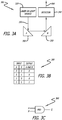
- FIG. 3A is a diagram depicting a disclosed photonic crystals logic device (i.e. an optical logic device) 300 having AND gate logic, in accordance with at least one example of the present disclosure.
- the optical logic device 300 is shown to comprise a source 320, two photonic crystals 330A, 330B, and a detector 340.
- the source 320 radiates at least one signal 350 towards the photonic crystals 330A, 330B. If the photonic crystals 330A, 330B sense a threshold strength of a physical phenomena (e.g., pressure, temperature, voltage, or vibration) associated with each of the photonic crystals 330A, 330B, the photonic crystals 330A, 330B are activated and, as such, will reflect the signal 350. However, if the photonic crystals 330A, 330B do not sense a threshold strength of the physical phenomena associated with each of the photonic crystals 330A, 330B, the photonic crystals 330A, 330B are not activated and, as such, will not reflect the signal 350.
- a threshold strength of a physical phenomena e.g., pressure, temperature, voltage, or vibration
- both photonic crystals 330A, 330B sense a threshold strength for their corresponding physical phenomena and are activated to reflect the signal 350.
- the signal 350 is then shown to be reflected towards the detector 340.
- the detector 340 detects the signal 350 and outputs a response 360 indicating that the signal 350 was detected.
- the photonic crystals 330A, 330B do not sense a threshold strength for their corresponding physical phenomena, they will not be activated and will not reflect the signal 350. In these cases, the detector 340 will not detect the signal 350. The detector 340 will output a response 360 indicating that the signal 350 was not detected.
- FIG. 3B is a table 380 comprising AND gate logic, which corresponds to the logic of the photonic crystals logic device of FIG. 3A .
- the input columns contain a "1" when the corresponding photonic crystals 330A, 330B are activated and reflect the signal 350.
- the input columns contain a "0" when the corresponding photonic crystals 330A, 330B are not activated and do not reflect the signal 350.
- the output column values indicate the data contained in the response signal 360. In this case, the output column contains a "1" when the detector 340 detects the signal 350, and the output column contains a "0" when the detector 340 does not detect the signal 350.
- FIG. 3C is a conventional diagram of an AND gate 390.
- the AND gate 390 is shown to have a two inputs (A and B), and one output (Q).
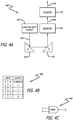
- FIG. 4A is a diagram showing a disclosed photonic crystals logic device (i.e. an optical logic device) 400 having NAND gate logic, in accordance with at least one example of the present disclosure.
- the optical logic device 400 is shown to comprise a source 420, two photonic crystals 430A, 430B, a detector 440, and an inverter 470.
- the source 420 radiates at least one signal 450 towards the photonic crystals 430A, 430B. If the photonic crystals 430A, 430B sense a threshold strength of a physical phenomena (e.g., pressure, temperature, voltage, or vibration) associated with each of the photonic crystals 430A, 430B, the photonic crystals 430A, 430B are activated and, as such, will reflect the signal 450. However, if the photonic crystals 430A, 430B do not sense a threshold strength of the physical phenomena associated with each of the photonic crystals 430A, 430B, the photonic crystals 430A, 430B are not activated and, as such, will not reflect the signal 450.
- a threshold strength of a physical phenomena e.g., pressure, temperature, voltage, or vibration
- both photonic crystals 430A, 430B sense a threshold strength for their corresponding physical phenomena and are activated to reflect the signal 450.
- the signal 450 is then shown to be reflected towards the detector 440.
- the detector 440 detects the signal 450 and outputs a response 460 indicating that the signal 450 was detected.
- the inverter 470 receives the response 460 and generates an inverted response 475.
- the photonic crystals 430A, 430B do not sense a threshold strength for their corresponding physical phenomena, they will not be activated and will not reflect the signal 450. In these cases, the detector 440 will not detect the signal 450. The detector 440 will output a response 460 indicating that the signal 450 was not detected. The inverter 470 then receives the response 460 and generates an inverted response 475.
- FIG. 4B is a table 480 comprising NAND gate logic, which corresponds to the logic of the photonic crystals logic device of FIG. 4A .
- the input columns contain a "1" when the corresponding photonic crystals 430A, 430B are activated and reflect the signal 450.
- the input columns contain a "0" when the corresponding photonic crystals 430A, 430B are not activated and do not reflect the signal 450.
- the output column values indicate the data contained in the response signal 475. In this case, the output column contains a "1" when the detector 440 does not detect the signal 450, and the output column contains a "0" when the detector 440 detects the signal 450.
- FIG. 4C is a conventional diagram of an NAND gate 490.
- the NAND gate 490 is shown to have a two inputs (A and B), and one output (Q).
- FIG. 5A is a diagram illustrating a disclosed photonic crystals logic device (i.e. an optical logic device) 500 having OR gate logic, in accordance with at least one example of the present disclosure.
- the optical logic device 500 is shown to comprise two sources 520, two photonic crystals 530A, 530B, and a detector 540.
- each of the two sources 520 radiate at least one signal 550 towards the photonic crystals 530A, 530B, respectively. If the photonic crystals 530A, 530B sense a threshold strength of a physical phenomena (e.g., pressure, temperature, voltage, or vibration) associated with each of the photonic crystals 530A, 530B, the photonic crystals 530A, 530B are activated and, as such, will reflect the signal 550.
- a physical phenomena e.g., pressure, temperature, voltage, or vibration
- the photonic crystals 530A, 530B do not sense a threshold strength of the physical phenomena associated with each of the photonic crystals 530A, 530B, the photonic crystals 530A, 530B are not activated and, as such, will not reflect the signal 550.
- both photonic crystals 530A, 530B sense a threshold strength for their corresponding physical phenomena and are activated to reflect the signal 550.
- the signal 550 is then shown to be reflected towards the detector 540.
- the detector 540 detects the signal 550 and outputs a response 560 indicating that the signal 550 was detected.
- both of the photonic crystals 530A, 530B do not sense a threshold strength for their corresponding physical phenomena, they will not be activated and will not reflect the signal 550. In these cases, the detector 540 will not detect the signal 550. The detector 540 will output a response 560 indicating that a signal 550 was not detected.
- FIG. 5B is a table 580 comprising OR gate logic, which corresponds to the logic of the photonic crystals logic device of FIG. 5A .
- the input columns contain a "1" when the corresponding photonic crystals 530A, 530B are activated and reflect the signal 550.
- the input columns contain a "0" when the corresponding photonic crystals 530A, 530B are not activated and do not reflect the signal 550.
- the output column values indicate the data contained in the response signal 560. In this case, the output column contains a "1" when the detector 540 detects the signal 550, and the output column contains a "0" when the detector 540 does not detect the signal 550.
- FIG. 5C is a conventional diagram of an OR gate 590.
- the OR gate 590 is shown to have a two inputs (A and B), and one output (Q).
- FIG. 6A is a diagram showing a disclosed photonic crystals logic device (i.e. an optical logic device) 600 having NOR gate logic, in accordance with at least one example of the present disclosure.
- the optical logic device 600 is shown to comprise two sources 620, two photonic crystals 630A, 630B, a detector 540, and an inverter 670.
- each of the two sources 620 radiate at least one signal 650 towards the photonic crystals 630A, 630B, respectively. If the photonic crystals 630A, 630B sense a threshold strength of a physical phenomena (e.g., pressure, temperature, voltage, or vibration) associated with each of the photonic crystals 630A, 630B, the photonic crystals 630A, 630B are activated and, as such, will reflect the signal 650.
- a physical phenomena e.g., pressure, temperature, voltage, or vibration
- the photonic crystals 630A, 630B do not sense a threshold strength of the physical phenomena associated with each of the photonic crystals 630A, 630B, the photonic crystals 630A, 630B are not activated and, as such, will not reflect the signal 650.
- both photonic crystals 630A, 630B sense a threshold strength for their corresponding physical phenomena and are activated to reflect the signal 650.
- the signal 650 is then shown to be reflected towards the detector 640.
- the detector 640 detects the signal 650 and outputs a response 660 indicating that the signal 650 was detected.
- the inverter 670 receives the response 660 and generates an inverted response 675.
- both of the photonic crystals 630A, 630B do not sense a threshold strength for their corresponding physical phenomena, they will not be activated and will not reflect the signal 650. In these cases, the detector 640 will not detect the signal 650. The detector 640 will output a response 660 indicating that a signal 650 was not detected. The inverter 670 then receives the response 660 and generates an inverted response 675.
- FIG. 6B is a table 680 comprising NOR gate logic, which corresponds to the logic of the photonic crystals logic device of FIG. 6A .
- the input columns contain a "1" when the corresponding photonic crystals 630A, 630B are activated and reflect the signal 650.
- the input columns contain a "0" when the corresponding photonic crystals 630A, 630B are not activated and do not reflect the signal 650.
- the output column values indicate the data contained in the response signal 675. In this case, the output column contains a "1" when the detector 640 does not detect the signal 650, and the output column contains a "0" when the detector 640 detects the signal 650.
- FIG. 6C is a conventional diagram of an NOR gate 690.
- the NOR gate 690 is shown to have a two inputs (A and B), and one output (Q).
- FIG. 7 is a diagram showing a flow chart for the disclosed method 700 for a photonic crystals logic device (i.e. an optical logic device), in accordance with at least one example of the present disclosure.
- a photonic crystals logic device i.e. an optical logic device
- At the start 710 of the method at least one source radiates at least one signal 720. Then, at least one signal is reflected off of at least one photonic crystal, when at least one photonic crystal senses a physical phenomena of a threshold strength 730. At least one signal is not reflected off of at least one photonic crystal, when at least one photonic crystal does not sense a physical phenomena of a threshold strength 740. At least one detector then detects or does not detect at least one signal 750. Then, at least one detector outputs at least one response indicating that at least one signal was detected or not detected 760. In some cases, at least one inverter inverts at least one response 770. Then, the method 700 ends 780.
- FIG. 8A is a diagram illustrating a photonic crystal reflector component 800, which may be employed by the disclosed photonic crystals logic device (i.e. an optical logic device), in accordance with at least one example of the present disclosure.
- the system of the present disclosure may implement at least one disclosed optical logic device (which may each employ at least one photonic crystal reflector component 800) into a single chip design.
- the components i.e. source(s), photonic crystal(s), detector(s), and optional inverter(s)
- IC integrated circuit
- Complex logic can be achieved by employing a plurality of optical logic devices (which may each employ at least one photonic crystal reflector component 800) connected together within the chip.
- the logic may be altered by disabling (e.g., by blowing a fuse and/or by removal of at least one thermal and/or electrical contact by use of, for example, a micro-electro-mechanical systems (MEMS) switch), either permanently or not permanently, at least one of the photonic crystals of at least one of the optical logic devices housed within the chip, thereby creating a field programmable crystal array.
- MEMS micro-electro-mechanical systems
- the photonic crystal reflector component 800 is shown to include two internal plates 810, 820. Each of the plates 810, 820 work in conjunction as a single optical element utilized as part of a photonic crystals logic device.
- FIG. 8B is a diagram depicting the internal structure of the photonic crystal reflector component 800 of FIG. 8A , in accordance with at least one example of the present disclosure. In this figure, details of the two plates 810, 820 are shown.
- Clause 2 The method of Clause 1, wherein the method further comprises:
- Clause 3 The method of Clause 2, wherein the method further comprises:
- Clause 4 The method of Clause 1, wherein the at least one detector (140) is at least one of a light detector or a laser detector.
- Clause 5 The method of Clause 1, wherein the at least one signal is an electromagnetic signal.
- Clause 6 The method of Clause 1, wherein the at least one source (120) is at least one of a light source or a laser source.
- Clause 7 The method of Clause 1, wherein the at least one photonic crystal (130) is at least one of one dimensional, two dimensional, or three dimensional.
- Clause 8 The method of Clause 1, wherein the physical phenomena is one of pressure, temperature, voltage, or vibration.
- Clause 9 The method of Clause 1, wherein the method further comprises:
- Clause 10 The method of Clause 1, wherein the at least one source (120), the at least one photonic crystal (130), and the at least one detector (140) are housed within at least one integrated circuit (IC) chip.
- IC integrated circuit
- Clause 12 The device (100) of Clause 11, wherein the at least one detector (140) is further to output at least one response indicating that the at least one signal was one of detected or not detected.
- Clause 13 The device (100) of Clause 12, wherein the device (100) further comprises:
- Clause 14 The device (100) of Clause 11, wherein the at least one detector (140) is at least one of a light detector or a laser detector.
- Clause 15 The device (100) of Clause 11, wherein the at least one signal is an electromagnetic signal.
- Clause 16 The device (100) of Clause 11, wherein the at least one source (120) is at least one of a light source or a laser source.
- Clause 17 The device (100) of Clause 11, wherein the at least one photonic crystal (130) is at least one of one dimensional, two dimensional, or three dimensional.
- Clause 18 The device (100) of Clause 11, wherein the physical phenomena is one of pressure, temperature, voltage, or vibration.
- Clause 19 The device (100) of Clause 11, wherein at least one of the at least one photonic crystal (130) is disabled.
- Clause 20 The device (100) of Clause 11, wherein the at least one source (120), the at least one photonic crystal (130), and the at least one detector (140) are housed within at least one integrated circuit (IC) chip.
- IC integrated circuit
Landscapes
- Physics & Mathematics (AREA)
- General Physics & Mathematics (AREA)
- Nonlinear Science (AREA)
- Optics & Photonics (AREA)
- Optical Modulation, Optical Deflection, Nonlinear Optics, Optical Demodulation, Optical Logic Elements (AREA)
- Semiconductor Lasers (AREA)
Abstract
Description
- The present disclosure relates to photonic crystals. In particular, it relates to photonic crystals logic devices.
- The demand for high bandwidth has increased to reach the speed limit of electronic devices. Existing optical signal processing systems utilize digital gates that provide logic. Digital gates are complicated and require cumbersome electro-optic conversion, which introduce time delays and attenuate the signals. Existing solutions also use Semiconductor Optical Amplifiers (SOAs) to boost the attenuated signals. SOAs are good components for simultaneous modulation and amplification for multiplexed optical signal transmission. However, the utilization of cascading SOAs increases the distortion due to cross-modulation of the different channels. SOAs have higher noise, lower gain, moderate polarization dependence, and high nonlinearity with fast transient time that can distort the signals. This nonlinearity presents the most significant problem for optical communication applications. As such, there is a need for an improved optical logic device design.
- The present disclosure relates to a method, system, and apparatus for photonic crystals logic devices. In one or more examples, a method for an optical logic device comprises radiating, by at least one source, at least one signal. The method further comprises reflecting at least one signal off of at least one photonic crystal, when at least one photonic crystal senses a physical phenomena of a threshold strength. Also, the method comprises not reflecting at least one signal off of at least one photonic crystal, when at least one photonic crystal does not sense the physical phenomena of the threshold strength. Further, the method comprises detecting or not detecting, by at least one detector, at least one signal.
- In one or more examples, the method further comprises outputting, by at least one detector, at least one response indicating that at least one signal was detected or not detected. In at least one example, the method further comprises inverting, by at least one inverter, at least one response.
- In at least one example, at least one detector is a light detector and/or a laser detector. In some examples, at least one signal is an electromagnetic signal. In one or more examples, at least one source is a light source and/or a laser source. In at least one example, at least one photonic crystal is one dimensional (1D), two dimensional (2D), and/or three dimensional (3D). In some examples, the physical phenomena is pressure, temperature, voltage, or vibration.
- In one or more examples, the method further comprises disabling at least one photonic crystal. In some examples, at least one source, at least one photonic crystal, and at least one detector are housed together within at least one integrated circuit (IC) chip.
- In at least one example, an optical logic device comprises at least one source to radiate at least one signal. In one or more examples, at least one signal is reflected off of at least one photonic crystal, when at least one photonic crystal senses a physical phenomena of a threshold strength. In some examples, at least one signal is not reflected off of at least one photonic crystal, when at least one photonic crystal does not sense the physical phenomena of the threshold strength. The device further comprises at least one detector to detect or not detect at least one signal.
- In one or more examples, at least one detector is further to output at least one response indicating that at least one signal was detected or not detected. In at least one example, the device further comprises at least one inverter to invert at least one response. In some examples, at least one photonic crystal is disabled.
- The features, functions, and advantages can be achieved independently in various examples of the present disclosure or may be combined in yet other examples.
- These and other features, aspects, and advantages of the present disclosure will become better understood with regard to the following description, appended claims, and accompanying drawings where:
-
FIG. 1 is a diagram showing a disclosed photonic crystals logic device (i.e. an optical logic device), in accordance with at least one example of the present disclosure. -
FIG. 2 is a diagram illustrating a disclosed photonic crystals logic device, where each of the photonic crystals senses a different physical phenomena, in accordance with at least one example of the present disclosure. -
FIG. 3A is a diagram depicting a disclosed photonic crystals logic device having AND gate logic, in accordance with at least one example of the present disclosure. -
FIG. 3B is a table comprising AND gate logic, which corresponds to the logic of the photonic crystals logic device ofFIG. 3A . -
FIG. 3C is a conventional diagram of an AND gate. -
FIG. 4A is a diagram showing a disclosed photonic crystals logic device having NAND gate logic, in accordance with at least one example of the present disclosure. -
FIG. 4B is a table comprising NAND gate logic, which corresponds to the logic of the photonic crystals logic device ofFIG. 4A . -
FIG. 4C is a conventional diagram of an NAND gate. -
FIG. 5A is a diagram illustrating a disclosed photonic crystals logic device having OR gate logic, in accordance with at least one example of the present disclosure. -
FIG. 5B is a table comprising OR gate logic, which corresponds to the logic of the photonic crystals logic device ofFIG. 5A . -
FIG. 5C is a conventional diagram of an OR gate. -
FIG. 6A is a diagram showing a disclosed photonic crystals logic device having NOR gate logic, in accordance with at least one example of the present disclosure. -
FIG. 6B is a table comprising NOR gate logic, which corresponds to the logic of the photonic crystals logic device ofFIG. 6A . -
FIG. 6C is a conventional diagram of an NOR gate. -
FIG. 7 is a diagram showing a flow chart for the disclosed method for a photonic crystals logic device (i.e. an optical logic device), in accordance with at least one example of the present disclosure. -
FIG. 8A is a diagram illustrating a photonic crystal reflector component, which may be employed by the disclosed photonic crystals logic device (i.e. an optical logic device), in accordance with at least one example of the present disclosure. -
FIG. 8B is a diagram depicting the internal structure of the photonic crystal reflector component ofFIG. 8A , in accordance with at least one example of the present disclosure. - The methods and apparatus disclosed herein provide an operative system for photonic crystals logic devices. The system of the present disclosure provides all-optical gates constructed of a non-linear medium comprising photonic crystal mirrors that provide high bandwidth with low power consumption. In particular, the photonic crystal mirrors can produce logic by being activated (i.e. reflecting a signal) when the photonic crystal mirrors sense a threshold strength of a physical phenomena (e.g., pressure, temperature, voltage, or vibration) and by not being activated (i.e. not reflecting a signal) when the photonic crystal mirrors do not sense a threshold strength of the physical phenomena.
- As previously mentioned above, the demand for high bandwidth has increased to reach the speed limit of electronic devices. All-optical signal processing with all-optical logic gates that operate at a high bit rate can address this bandwidth need. To make all-optical systems, it is necessary that all components be optical elements. The system of present disclosure makes this possible by employing all-optical gates, which are the key elements to achieving all-optical functions.
- The system of the present disclosure may employ wafer-scale integration for the all-optical gates to facilitate better performance by improving power efficiency and reliability, which are critical for optical communications applications. The use of photonic crystals makes the packaging and assembly of all-optical gates simpler and more robust, which are ideal characteristics for demanding aerospace environments.
- The present disclosure utilizes the implementation of systems-on-a-chip to provide a compact and cost-effective way of improving performance with better efficiency, higher reliability, and robustness. It should be noted that a single chip design has minimal optical interfaces, which aerospace environments demand. This technology can be utilized in ground breaking advancements in digital beam forming, which may be used in space applications.
- In the following description, numerous details are set forth in order to provide a more thorough description of the system. It will be apparent, however, to one skilled in the art, that the disclosed system may be practiced without these specific details. In the other instances, well known features have not been described in detail so as not to unnecessarily obscure the system.
- Examples of the present disclosure may be described herein in terms of functional and/or logical components and various processing steps. It should be appreciated that such components may be realized by any number of hardware, software, and/or firmware components configured to perform the specified functions. For example, an example of the present disclosure may employ various integrated circuit components (e.g., memory elements, digital signal processing elements, logic elements, look-up tables, or the like), which may carry out a variety of functions under the control of one or more processors, microprocessors, or other control devices. In addition, those skilled in the art will appreciate that examples of the present disclosure may be practiced in conjunction with other components, and that the system described herein is merely one example example of the present disclosure.
- For the sake of brevity, conventional techniques and components related to optical signal processing systems, and other functional aspects of the system (and the individual operating components of the systems) may not be described in detail herein. Furthermore, the connecting lines shown in the various figures contained herein are intended to represent example functional relationships and/or physical couplings between the various elements. It should be noted that many alternative or additional functional relationships or physical connections may be present in an example of the present disclosure.
-
FIG. 1 is a diagram showing a disclosed photonic crystals logic device (i.e. an optical logic device) 100, in accordance with at least one example of the present disclosure. In this figure, theoptical logic device 100 is shown to comprise asource 120, fourphotonic crystals 130, and adetector 140. - In one or more examples, the
source 120 may be a light source or a laser source. In some examples, theoptical logic device 100 may employ more than onesource 120, as is shown inFIG. 1 . In at least one example, thephotonic crystals 130 may be one dimensional (1D) photonic crystals, two dimensional (2D) photonic crystals, or three dimensional (3D) photonic crystals. In some examples, theoptical logic device 100 may employ more than or less than fourphotonic crystals 130, as is shown inFIG. 1 . In one or more examples, thedetector 140 may be a light detector or a laser detector. In some examples, theoptical logic device 100 may employ more than onedetector 140, as is shown inFIG. 1 . - During operation of the
optical logic device 100, thesource 120 radiates at least onesignal 150 towards thephotonic crystals 130. In one or more examples thesignal 150 is an electromagnetic signal, such as an optical signal or light. If thephotonic crystals 130 sense a threshold strength of a physical phenomena (e.g., pressure, temperature, voltage, or vibration) associated with each of thephotonic crystals 130, thephotonic crystals 130 are activated and, as such, will reflect thesignal 150. However, if thephotonic crystals 130 do not sense a threshold strength of the physical phenomena associated with each of thephotonic crystals 130, thephotonic crystals 130 are not activated and, as such, will not reflect thesignal 150. - As shown in
FIG. 1 , all fourphotonic crystals 130 sense a threshold strength for their corresponding physical phenomena and are activated to reflect thesignal 150. Thesignal 150 is then shown to be reflected towards thedetector 140. Thedetector 140 then detects thesignal 150 and outputs aresponse 160 indicating that thesignal 150 was detected. - It should be noted that if one or more of the
photonic crystals 130 do not sense a threshold strength for their corresponding physical phenomena, they will not be activated and will not reflect thesignal 150. In these cases, thedetector 140 will not detect thesignal 150. Thedetector 140 will output aresponse 160 indicating that thesignal 150 was not detected. -
FIG. 2 is a diagram illustrating a disclosed photonic crystals logic device (i.e. an optical logic device) 200, where each of thephotonic crystals optical logic device 200 is shown to comprise asource 220, fourphotonic crystals detector 240. For this example, each of thephotonic crystals FIG. 2 ,photonic crystal 230A is activated by a threshold strength for pressure (e.g., a specific value of pounds per square inch (psi)),photonic crystal 230B is activated by a threshold strength for temperature (e.g., a specific value of degrees Kelvin (K)),photonic crystal 230C is activated by a threshold strength for vibration (e.g., a specific value of power spectral density (psd)), andphotonic crystal 230D is activated by a threshold strength for voltage (e.g., a specific value of volts (V)). - During operation of the
optical logic device 200, thesource 220 radiates at least onesignal 250 towards thephotonic crystals signal 250. However, if the photonic crystals 230 do not sense a threshold strength of the physical phenomena associated with each of the photonic crystals 230, the photonic crystals 230 are not activated and, as such, will not reflect thesignal 250. For example, ifphotonic crystal 230A senses a threshold strength of pressure (e.g., a specific value of psi), thephotonic crystal 230A will be activated and reflect thesignal 250, as is shown inFIG. 2 . Also, ifphotonic crystal 230B senses a threshold strength of temperature (e.g., a specific value of K), thephotonic crystal 230B will be activated and reflect thesignal 250, as is shown inFIG. 2 . In addition, ifphotonic crystal 230C senses a threshold strength of vibration (e.g., a specific value of psd), thephotonic crystal 230C will be activated and reflect thesignal 250, as is shown inFIG. 2 . Further, ifphotonic crystal 230D senses a threshold strength of voltage (e.g., a specific value of V), thephotonic crystal 230D will be activated and reflect thesignal 250, as is shown inFIG. 2 . - As such, as is shown in
FIG. 2 , all fourphotonic crystals signal 250. Thesignal 250 is then shown to be reflected towards thedetector 240. Then, thedetector 240 detects thesignal 250 and outputs aresponse 260 indicating that thesignal 250 was detected. - It should be noted that if one or more of the
photonic crystals signal 250. In these cases, thedetector 240 will not detect thesignal 250. Thedetector 240 will output aresponse 260 indicating that thesignal 250 was not detected. -
FIG. 3A is a diagram depicting a disclosed photonic crystals logic device (i.e. an optical logic device) 300 having AND gate logic, in accordance with at least one example of the present disclosure. In this figure, theoptical logic device 300 is shown to comprise asource 320, two photonic crystals 330A, 330B, and adetector 340. - During operation of the
optical logic device 300, thesource 320 radiates at least onesignal 350 towards the photonic crystals 330A, 330B. If the photonic crystals 330A, 330B sense a threshold strength of a physical phenomena (e.g., pressure, temperature, voltage, or vibration) associated with each of the photonic crystals 330A, 330B, the photonic crystals 330A, 330B are activated and, as such, will reflect thesignal 350. However, if the photonic crystals 330A, 330B do not sense a threshold strength of the physical phenomena associated with each of the photonic crystals 330A, 330B, the photonic crystals 330A, 330B are not activated and, as such, will not reflect thesignal 350. - As shown in
FIG. 3A , both photonic crystals 330A, 330B sense a threshold strength for their corresponding physical phenomena and are activated to reflect thesignal 350. Thesignal 350 is then shown to be reflected towards thedetector 340. Thedetector 340 then detects thesignal 350 and outputs aresponse 360 indicating that thesignal 350 was detected. - It should be noted that if one or both of the photonic crystals 330A, 330B do not sense a threshold strength for their corresponding physical phenomena, they will not be activated and will not reflect the
signal 350. In these cases, thedetector 340 will not detect thesignal 350. Thedetector 340 will output aresponse 360 indicating that thesignal 350 was not detected. -
FIG. 3B is a table 380 comprising AND gate logic, which corresponds to the logic of the photonic crystals logic device ofFIG. 3A . In table 380, the input columns contain a "1" when the corresponding photonic crystals 330A, 330B are activated and reflect thesignal 350. And, the input columns contain a "0" when the corresponding photonic crystals 330A, 330B are not activated and do not reflect thesignal 350. The output column values indicate the data contained in theresponse signal 360. In this case, the output column contains a "1" when thedetector 340 detects thesignal 350, and the output column contains a "0" when thedetector 340 does not detect thesignal 350. -
FIG. 3C is a conventional diagram of an ANDgate 390. In this figure, the ANDgate 390 is shown to have a two inputs (A and B), and one output (Q). -
FIG. 4A is a diagram showing a disclosed photonic crystals logic device (i.e. an optical logic device) 400 having NAND gate logic, in accordance with at least one example of the present disclosure. In this figure, theoptical logic device 400 is shown to comprise asource 420, two photonic crystals 430A, 430B, adetector 440, and aninverter 470. - During operation of the
optical logic device 400, thesource 420 radiates at least onesignal 450 towards the photonic crystals 430A, 430B. If the photonic crystals 430A, 430B sense a threshold strength of a physical phenomena (e.g., pressure, temperature, voltage, or vibration) associated with each of the photonic crystals 430A, 430B, the photonic crystals 430A, 430B are activated and, as such, will reflect thesignal 450. However, if the photonic crystals 430A, 430B do not sense a threshold strength of the physical phenomena associated with each of the photonic crystals 430A, 430B, the photonic crystals 430A, 430B are not activated and, as such, will not reflect thesignal 450. - As shown in
FIG. 4A , both photonic crystals 430A, 430B sense a threshold strength for their corresponding physical phenomena and are activated to reflect thesignal 450. Thesignal 450 is then shown to be reflected towards thedetector 440. Thedetector 440 then detects thesignal 450 and outputs aresponse 460 indicating that thesignal 450 was detected. Theinverter 470 receives theresponse 460 and generates aninverted response 475. - It should be noted that if one or both of the photonic crystals 430A, 430B do not sense a threshold strength for their corresponding physical phenomena, they will not be activated and will not reflect the
signal 450. In these cases, thedetector 440 will not detect thesignal 450. Thedetector 440 will output aresponse 460 indicating that thesignal 450 was not detected. Theinverter 470 then receives theresponse 460 and generates aninverted response 475. -
FIG. 4B is a table 480 comprising NAND gate logic, which corresponds to the logic of the photonic crystals logic device ofFIG. 4A . In table 480, the input columns contain a "1" when the corresponding photonic crystals 430A, 430B are activated and reflect thesignal 450. And, the input columns contain a "0" when the corresponding photonic crystals 430A, 430B are not activated and do not reflect thesignal 450. The output column values indicate the data contained in theresponse signal 475. In this case, the output column contains a "1" when thedetector 440 does not detect thesignal 450, and the output column contains a "0" when thedetector 440 detects thesignal 450. -
FIG. 4C is a conventional diagram of anNAND gate 490. In this figure, theNAND gate 490 is shown to have a two inputs (A and B), and one output (Q). -
FIG. 5A is a diagram illustrating a disclosed photonic crystals logic device (i.e. an optical logic device) 500 having OR gate logic, in accordance with at least one example of the present disclosure. In this figure, theoptical logic device 500 is shown to comprise twosources 520, two photonic crystals 530A, 530B, and adetector 540. - During operation of the
optical logic device 500, each of the twosources 520 radiate at least onesignal 550 towards the photonic crystals 530A, 530B, respectively. If the photonic crystals 530A, 530B sense a threshold strength of a physical phenomena (e.g., pressure, temperature, voltage, or vibration) associated with each of the photonic crystals 530A, 530B, the photonic crystals 530A, 530B are activated and, as such, will reflect thesignal 550. However, if the photonic crystals 530A, 530B do not sense a threshold strength of the physical phenomena associated with each of the photonic crystals 530A, 530B, the photonic crystals 530A, 530B are not activated and, as such, will not reflect thesignal 550. - As shown in
FIG. 5A , both photonic crystals 530A, 530B sense a threshold strength for their corresponding physical phenomena and are activated to reflect thesignal 550. Thesignal 550 is then shown to be reflected towards thedetector 540. Thedetector 540 then detects thesignal 550 and outputs aresponse 560 indicating that thesignal 550 was detected. - It should be noted that if both of the photonic crystals 530A, 530B do not sense a threshold strength for their corresponding physical phenomena, they will not be activated and will not reflect the
signal 550. In these cases, thedetector 540 will not detect thesignal 550. Thedetector 540 will output aresponse 560 indicating that asignal 550 was not detected. -
FIG. 5B is a table 580 comprising OR gate logic, which corresponds to the logic of the photonic crystals logic device ofFIG. 5A . In table 580, the input columns contain a "1" when the corresponding photonic crystals 530A, 530B are activated and reflect thesignal 550. And, the input columns contain a "0" when the corresponding photonic crystals 530A, 530B are not activated and do not reflect thesignal 550. The output column values indicate the data contained in theresponse signal 560. In this case, the output column contains a "1" when thedetector 540 detects thesignal 550, and the output column contains a "0" when thedetector 540 does not detect thesignal 550. -
FIG. 5C is a conventional diagram of anOR gate 590. In this figure, theOR gate 590 is shown to have a two inputs (A and B), and one output (Q). -
FIG. 6A is a diagram showing a disclosed photonic crystals logic device (i.e. an optical logic device) 600 having NOR gate logic, in accordance with at least one example of the present disclosure. In this figure, theoptical logic device 600 is shown to comprise twosources 620, two photonic crystals 630A, 630B, adetector 540, and aninverter 670. - During operation of the
optical logic device 600, each of the twosources 620 radiate at least onesignal 650 towards the photonic crystals 630A, 630B, respectively. If the photonic crystals 630A, 630B sense a threshold strength of a physical phenomena (e.g., pressure, temperature, voltage, or vibration) associated with each of the photonic crystals 630A, 630B, the photonic crystals 630A, 630B are activated and, as such, will reflect thesignal 650. However, if the photonic crystals 630A, 630B do not sense a threshold strength of the physical phenomena associated with each of the photonic crystals 630A, 630B, the photonic crystals 630A, 630B are not activated and, as such, will not reflect thesignal 650. - As shown in
FIG. 6A , both photonic crystals 630A, 630B sense a threshold strength for their corresponding physical phenomena and are activated to reflect thesignal 650. Thesignal 650 is then shown to be reflected towards thedetector 640. Thedetector 640 then detects thesignal 650 and outputs aresponse 660 indicating that thesignal 650 was detected. Theinverter 670 receives theresponse 660 and generates aninverted response 675. - It should be noted that if both of the photonic crystals 630A, 630B do not sense a threshold strength for their corresponding physical phenomena, they will not be activated and will not reflect the
signal 650. In these cases, thedetector 640 will not detect thesignal 650. Thedetector 640 will output aresponse 660 indicating that asignal 650 was not detected. Theinverter 670 then receives theresponse 660 and generates aninverted response 675. -
FIG. 6B is a table 680 comprising NOR gate logic, which corresponds to the logic of the photonic crystals logic device ofFIG. 6A . In table 680, the input columns contain a "1" when the corresponding photonic crystals 630A, 630B are activated and reflect thesignal 650. And, the input columns contain a "0" when the corresponding photonic crystals 630A, 630B are not activated and do not reflect thesignal 650. The output column values indicate the data contained in theresponse signal 675. In this case, the output column contains a "1" when thedetector 640 does not detect thesignal 650, and the output column contains a "0" when thedetector 640 detects thesignal 650. -
FIG. 6C is a conventional diagram of an NORgate 690. In this figure, the NORgate 690 is shown to have a two inputs (A and B), and one output (Q). -
FIG. 7 is a diagram showing a flow chart for the disclosedmethod 700 for a photonic crystals logic device (i.e. an optical logic device), in accordance with at least one example of the present disclosure. At thestart 710 of the method, at least one source radiates at least onesignal 720. Then, at least one signal is reflected off of at least one photonic crystal, when at least one photonic crystal senses a physical phenomena of athreshold strength 730. At least one signal is not reflected off of at least one photonic crystal, when at least one photonic crystal does not sense a physical phenomena of athreshold strength 740. At least one detector then detects or does not detect at least onesignal 750. Then, at least one detector outputs at least one response indicating that at least one signal was detected or not detected 760. In some cases, at least one inverter inverts at least oneresponse 770. Then, themethod 700 ends 780. -
FIG. 8A is a diagram illustrating a photoniccrystal reflector component 800, which may be employed by the disclosed photonic crystals logic device (i.e. an optical logic device), in accordance with at least one example of the present disclosure. - The system of the present disclosure may implement at least one disclosed optical logic device (which may each employ at least one photonic crystal reflector component 800) into a single chip design. For this implementation, the components (i.e. source(s), photonic crystal(s), detector(s), and optional inverter(s)) of each of the optical logic devices are all housed within a single integrated circuit (IC) chip, such as a field programmable crystal array.
- Complex logic can be achieved by employing a plurality of optical logic devices (which may each employ at least one photonic crystal reflector component 800) connected together within the chip. In one or more examples, the logic may be altered by disabling (e.g., by blowing a fuse and/or by removal of at least one thermal and/or electrical contact by use of, for example, a micro-electro-mechanical systems (MEMS) switch), either permanently or not permanently, at least one of the photonic crystals of at least one of the optical logic devices housed within the chip, thereby creating a field programmable crystal array.
- In this figure, the photonic
crystal reflector component 800 is shown to include twointernal plates plates -
FIG. 8B is a diagram depicting the internal structure of the photoniccrystal reflector component 800 ofFIG. 8A , in accordance with at least one example of the present disclosure. In this figure, details of the twoplates - Although particular examples have been shown and described, it should be understood that the above discussion is not intended to limit the scope of these examples. While examples and variations of the many aspects of the invention have been disclosed and described herein, such disclosure is provided for purposes of explanation and illustration only. Thus, various changes and modifications may be made without departing from the scope of the claims.
- Although particular examples have been shown and described, it should be understood that the above discussion is not intended to limit the scope of these examples. While examples and variations of the many aspects of the present disclosure have been disclosed and described herein, such disclosure is provided for purposes of explanation and illustration only. Thus, various changes and modifications may be made without departing from the scope of the claims.
- Where methods described above indicate certain events occurring in certain order, those of ordinary skill in the art having the benefit of this disclosure would recognize that the ordering may be modified and that such modifications are in accordance with the variations of the present disclosure. Additionally, parts of methods may be performed concurrently in a parallel process when possible, as well as performed sequentially. In addition, more parts or less part of the methods may be performed.
- Accordingly, examples are intended to exemplify alternatives, modifications, and equivalents that may fall within the scope of the claims.
- Although certain illustrative examples and methods have been disclosed herein, it can be apparent from the foregoing disclosure to those skilled in the art that variations and modifications of such examples and methods can be made without departing from the true spirit and scope of the art disclosed. Many other examples of the art disclosed exist, each differing from others in matters of detail only. Accordingly, it is intended that the art disclosed shall be limited only to the extent required by the appended claims and the rules and principles of applicable law.
- Further, the disclosure comprises examples according to the following clauses:
-
Clause 1. A method for an optical logic device (100), the method comprising:- radiating, by at least one source (120), at least one signal;
- reflecting the at least one signal off of at least one photonic crystal (130), when the at least one photonic crystal (130) senses a physical phenomena of a threshold strength;
- not reflecting the at least one signal off of the at least one photonic crystal (130), when the at least one photonic crystal (130) does not sense the physical phenomena of the threshold strength; and
- detecting or not detecting, by at least one detector (140), the at least one signal.
- Clause 2. The method of
Clause 1, wherein the method further comprises: - outputting, by the at least one detector (140), at least one response indicating that the at least one signal was one of detected or not detected.
- Clause 3. The method of Clause 2, wherein the method further comprises:
- inverting, by at least one inverter (470), the at least one response.
- Clause 4. The method of
Clause 1, wherein the at least one detector (140) is at least one of a light detector or a laser detector. - Clause 5. The method of
Clause 1, wherein the at least one signal is an electromagnetic signal. - Clause 6. The method of
Clause 1, wherein the at least one source (120) is at least one of a light source or a laser source. - Clause 7. The method of
Clause 1, wherein the at least one photonic crystal (130) is at least one of one dimensional, two dimensional, or three dimensional. - Clause 8. The method of
Clause 1, wherein the physical phenomena is one of pressure, temperature, voltage, or vibration. - Clause 9. The method of
Clause 1, wherein the method further comprises: - disabling, at least one of the at least one photonic crystal (130).
-
Clause 10. The method ofClause 1, wherein the at least one source (120), the at least one photonic crystal (130), and the at least one detector (140) are housed within at least one integrated circuit (IC) chip. - Clause 11. An optical logic device (100), the device (100) comprising:
- at least one source (120) to radiate at least one signal,
- wherein the at least one signal is reflected off of at least one photonic crystal (130), when the at least one photonic crystal (130) senses a physical phenomena of a threshold strength,
- wherein the at least one signal is not reflected off of the at least one photonic crystal (130), when the at least one photonic crystal (130) does not sense the physical phenomena of the threshold strength; and
- at least one detector (140) to detect or to not detect the at least one signal.
- Clause 12. The device (100) of Clause 11, wherein the at least one detector (140) is further to output at least one response indicating that the at least one signal was one of detected or not detected.
- Clause 13. The device (100) of Clause 12, wherein the device (100) further comprises:
- at least one inverter (470) to invert the at least one response.
- Clause 14. The device (100) of Clause 11, wherein the at least one detector (140) is at least one of a light detector or a laser detector.
- Clause 15. The device (100) of Clause 11, wherein the at least one signal is an electromagnetic signal.
- Clause 16. The device (100) of Clause 11, wherein the at least one source (120) is at least one of a light source or a laser source.
- Clause 17. The device (100) of Clause 11, wherein the at least one photonic crystal (130) is at least one of one dimensional, two dimensional, or three dimensional.
- Clause 18. The device (100) of Clause 11, wherein the physical phenomena is one of pressure, temperature, voltage, or vibration.
- Clause 19. The device (100) of Clause 11, wherein at least one of the at least one photonic crystal (130) is disabled.
- Clause 20. The device (100) of Clause 11, wherein the at least one source (120), the at least one photonic crystal (130), and the at least one detector (140) are housed within at least one integrated circuit (IC) chip.
Claims (15)
- A method for an optical logic device (100), the method comprising:radiating, by at least one source (120), at least one signal;reflecting the at least one signal off of at least one photonic crystal (130), when the at least one photonic crystal (130) senses a physical phenomena of a threshold strength;not reflecting the at least one signal off of the at least one photonic crystal (130), when the at least one photonic crystal (130) does not sense the physical phenomena of the threshold strength; anddetecting or not detecting, by at least one detector (140), the at least one signal.
- The method of claim 1, wherein the method further comprises:outputting, by the at least one detector (140), at least one response indicating that the at least one signal was one of detected or not detected.
- The method of claim 2, wherein the method further comprises:inverting, by at least one inverter (470), the at least one response.
- The method of any one of claims 1-3, wherein the at least one detector (140) is at least one of a light detector or a laser detector.
- The method of any one of claims 1-4, wherein the at least one signal is an electromagnetic signal, the at least one source (120) is at least one of a light source or a laser source and the at least one photonic crystal (130) is at least one of one dimensional, two dimensional, or three dimensional.
- The method of any one of claims 1-5, wherein the physical phenomena is one of pressure, temperature, voltage, or vibration.
- The method of any one of claims 1-6, wherein the method further comprises:disabling, at least one of the at least one photonic crystal (130).
- An optical logic device (100), the device (100) comprising:at least one source (120) to radiate at least one signal,wherein the at least one signal is reflected off of at least one photonic crystal (130), when the at least one photonic crystal (130) senses a physical phenomena of a threshold strength,wherein the at least one signal is not reflected off of the at least one photonic crystal (130), when the at least one photonic crystal (130) does not sense the physical phenomena of the threshold strength; andat least one detector (140) to detect or to not detect the at least one signal.
- The device (100) of claim 8, wherein the at least one detector (140) provides at least one response indicating that the at least one signal was one of detected or not detected.
- The device (100) of claim 9, wherein the device (100) further comprises:at least one inverter (470) to invert the at least one response.
- The device (100) of any one of claims 8-10, wherein the at least one detector (140) is at least one of a light detector or a laser detector.
- The device (100) of any one of claims 8-11, wherein the at least one signal is an electromagnetic signal.
- The device (100) of any one of claims 8-12, wherein the at least one source (120) is at least one of a light source or a laser source.
- The device (100) of any one of claims 8-13, wherein the physical phenomena is one of pressure, temperature, voltage, or vibration.
- The device (100) of any one of claims 8-14, wherein the at least one source (120), the at least one photonic crystal (130), and the at least one detector (140) are housed within at least one integrated circuit (IC) chip.
Applications Claiming Priority (1)
| Application Number | Priority Date | Filing Date | Title |
|---|---|---|---|
| US15/178,464 US11126065B2 (en) | 2016-06-09 | 2016-06-09 | Photonic crystals logic devices |
Publications (2)
| Publication Number | Publication Date |
|---|---|
| EP3255490A1 true EP3255490A1 (en) | 2017-12-13 |
| EP3255490B1 EP3255490B1 (en) | 2021-01-27 |
Family
ID=58709741
Family Applications (1)
| Application Number | Title | Priority Date | Filing Date |
|---|---|---|---|
| EP17166776.9A Active EP3255490B1 (en) | 2016-06-09 | 2017-04-18 | Photonic crystals logic devices |
Country Status (6)
| Country | Link |
|---|---|
| US (1) | US11126065B2 (en) |
| EP (1) | EP3255490B1 (en) |
| JP (1) | JP7013140B2 (en) |
| CN (1) | CN107490919B (en) |
| CA (1) | CA2965948C (en) |
| RU (1) | RU2727857C2 (en) |
Family Cites Families (26)
| Publication number | Priority date | Publication date | Assignee | Title |
|---|---|---|---|---|
| JPS62183172A (en) | 1986-02-06 | 1987-08-11 | Matsushita Electronics Corp | semiconductor equipment |
| JPH04115240A (en) | 1990-09-05 | 1992-04-16 | Nec Ibaraki Ltd | Optical logical arithmetic unit |
| JPH0527290A (en) | 1991-07-24 | 1993-02-05 | Ricoh Co Ltd | Optical A / D converter |
| JPH06242481A (en) | 1993-02-17 | 1994-09-02 | Alps Electric Co Ltd | Optical gate array element |
| JP2692591B2 (en) | 1994-06-30 | 1997-12-17 | 株式会社日立製作所 | Optical memory device and optical circuit using the same |
| JP4619507B2 (en) * | 2000-09-26 | 2011-01-26 | 浜松ホトニクス株式会社 | Optical fiber coupling device, wavelength tunable device, pressure sensor, acceleration sensor, and optical device |
| US20030072519A1 (en) * | 2001-10-17 | 2003-04-17 | Bolanos Miguel Holgado | Photonic device, optical logic circuit incorporting the photonic device and method of manufacturing thereof |
| US7376293B2 (en) * | 2003-07-18 | 2008-05-20 | Network Intergrity Systems Inc. | Remote location of active section of fiber in a multimode intrusion detection system |
| US7480319B2 (en) * | 2003-10-15 | 2009-01-20 | California Institute Of Technology | Optical switches and logic and methods of implementation |
| ITMI20041286A1 (en) * | 2004-06-24 | 2004-09-24 | Marconi Comm Spa | RECONFIGURABLE AND REGENERATIVE ULTRA-FAST OPTICAL LOGIC DOORS |
| US7315663B2 (en) * | 2005-06-10 | 2008-01-01 | Hewlett-Packard Development Company, L.P. | Electronically controlled photonic crystal optical switch |
| US7409131B2 (en) * | 2006-02-14 | 2008-08-05 | Coveytech, Llc | All-optical logic gates using nonlinear elements—claim set V |
| US7826058B1 (en) * | 2006-05-19 | 2010-11-02 | Bowling Green State University | All optical and hybrid reflection switch at a semiconductor/glass interface due to laser beam intersection |
| US9036253B2 (en) * | 2006-10-06 | 2015-05-19 | The Regents Of The University Of California | Photonic devices based on vertical-cavity semiconductor optical amplifiers |
| US7630589B2 (en) | 2007-01-09 | 2009-12-08 | The Board Of Trustees Of The Leland Stanford Junior University | Photonic crystal structure sensor |
| EP2156471A2 (en) * | 2007-05-07 | 2010-02-24 | Nxp B.V. | A photosensitive device and a method of manufacturing a photosensitive device |
| CN102576979B (en) * | 2009-09-01 | 2014-12-17 | 日本电信电话株式会社 | Photonic crystal device |
| US9482927B2 (en) * | 2009-10-26 | 2016-11-01 | The Boeing Company | Optical sensor interrogation system |
| US8494312B2 (en) | 2010-08-18 | 2013-07-23 | The Boeing Company | Magnetically actuated photonic crystal sensor |
| US20120325001A1 (en) * | 2011-06-27 | 2012-12-27 | The Boeing Company | Optical sensor systems and methods |
| CN102323707A (en) * | 2011-09-26 | 2012-01-18 | 北京邮电大学 | A photonic crystal all-optical XOR logic gate structure based on the principle of interference |
| US9007227B2 (en) | 2012-01-04 | 2015-04-14 | The Boeing Company | Multimode fiber interrogator |
| US8633729B1 (en) * | 2012-01-27 | 2014-01-21 | Rockwell Collins, Inc. | Localized plasmon-polariton (LPP) logic gates and computing |
| US8935777B2 (en) | 2012-02-17 | 2015-01-13 | Ebay Inc. | Login using QR code |
| US9086331B2 (en) * | 2012-10-23 | 2015-07-21 | The Boeing Company | Optical fiber coupled photonic crystal slab strain sensor system |
| CN105404074B (en) * | 2015-12-23 | 2018-10-23 | 山东大学 | 2 D photon crystal logical AND gate based on auto-collimation interference effect |
-
2016
- 2016-06-09 US US15/178,464 patent/US11126065B2/en active Active
-
2017
- 2017-04-18 EP EP17166776.9A patent/EP3255490B1/en active Active
- 2017-04-18 RU RU2017113422A patent/RU2727857C2/en active
- 2017-04-20 JP JP2017083498A patent/JP7013140B2/en active Active
- 2017-05-01 CA CA2965948A patent/CA2965948C/en active Active
- 2017-05-31 CN CN201710396837.6A patent/CN107490919B/en active Active
Non-Patent Citations (5)
| Title |
|---|
| GLUSHKO, E. YA ET AL., SPIE, PO BOX 10 BELLINGHAM WA 98227-0010, USA, 1 January 2010 (2010-01-01), XP040551057 * |
| GLUSHKO, E. YA, SPIE, PO BOX 10 BELLINGHAM WA 98227-0010 USA, 1 January 2008 (2008-01-01), XP040434342 * |
| SALMANPOUR ARYAN ET AL: "Photonic crystal logic gates: an overview", OPTICAL AND QUANTUM ELECTRONICS, CHAPMAN AND HALL, LONDON, GB, vol. 47, no. 7, 25 December 2014 (2014-12-25), pages 2249 - 2275, XP035518136, ISSN: 0306-8919, [retrieved on 20141225], DOI: 10.1007/S11082-014-0102-1 * |
| SHAIK ENAUL HAQ ET AL: "Improved design of all-optical photonic crystal logic gates using T-shaped waveguide", OPTICAL AND QUANTUM ELECTRONICS, CHAPMAN AND HALL, LONDON, GB, vol. 48, no. 1, 19 December 2015 (2015-12-19), pages 1 - 15, XP035927166, ISSN: 0306-8919, [retrieved on 20151219], DOI: 10.1007/S11082-015-0279-Y * |
| SHARIFI HOJJAT ET AL: "A new design procedure for all-optical photonic crystal logic gates and functions based on threshold logic", OPTICS COMMUNICATIONS, ELSEVIER, AMSTERDAM, NL, vol. 370, 16 March 2016 (2016-03-16), pages 231 - 238, XP029485491, ISSN: 0030-4018, DOI: 10.1016/J.OPTCOM.2016.03.020 * |
Also Published As
| Publication number | Publication date |
|---|---|
| BR102017012035A2 (en) | 2017-12-19 |
| RU2017113422A3 (en) | 2020-06-02 |
| CN107490919A (en) | 2017-12-19 |
| US11126065B2 (en) | 2021-09-21 |
| US20170357143A1 (en) | 2017-12-14 |
| CN107490919B (en) | 2022-06-17 |
| CA2965948C (en) | 2021-07-13 |
| EP3255490B1 (en) | 2021-01-27 |
| RU2727857C2 (en) | 2020-07-24 |
| JP7013140B2 (en) | 2022-01-31 |
| CA2965948A1 (en) | 2017-12-09 |
| RU2017113422A (en) | 2018-10-18 |
| JP2017219831A (en) | 2017-12-14 |
Similar Documents
| Publication | Publication Date | Title |
|---|---|---|
| US10498544B2 (en) | Security device having physical unclonable function | |
| US9235542B2 (en) | Signal switching circuit and peripheral component interconnect express connector assembly having the signal switching circuit | |
| US20190013870A1 (en) | Photonic integrated circuit and optical transmitter | |
| JP4656563B2 (en) | Method and apparatus for silicon-based photoexcitation amplification using stimulated scattering | |
| US9875994B2 (en) | Multi-chip package, system and test method thereof | |
| CN104503098A (en) | Laser beam combination system | |
| US7554351B2 (en) | Chip burning system for burning chips of motherboard | |
| EP3255490A1 (en) | Photonic crystals logic devices | |
| CN101682317B (en) | Method and apparatus for programmable delay having fine delay resolution | |
| KR102501479B1 (en) | Redirected light modulator output | |
| US20130258630A1 (en) | Hard disk drive connector | |
| US11624782B2 (en) | Core partition circuit and testing device | |
| CN103220121B (en) | A kind of many radio systems and radio-frequency module | |
| US8118214B2 (en) | Method and system for generating electronic keys | |
| CN220491159U (en) | Logic gate clock circuit, optical signal frequency division tool | |
| CN109599738B (en) | Optical pulse compressor | |
| KR100660833B1 (en) | I / O control clock generation method that can secure timing margin and reduce power noise and power consumption, and semiconductor memory device implemented accordingly | |
| BR102017012035B1 (en) | METHOD FOR AN OPTICAL LOGIC DEVICE AND OPTICAL LOGIC DEVICE | |
| US8855836B2 (en) | Methods and systems for implementing software-selectable multipurpose aircraft pins | |
| CN103197453B (en) | Wavelength blocker and wavelength blocking system based on liquid crystal on silicon technology | |
| US10917075B2 (en) | Oscillator apparatus capable of protecting circuit element(s) within oscillator of oscillator apparatus from damage of signal glitch | |
| US10425183B2 (en) | Optical transmission method and apparatus | |
| RU2210121C1 (en) | Radio-signal dynamic memory device with binary fiber-optic structure | |
| KR0175614B1 (en) | Optical amplifier using 2ñ 2 polarizing beam splitter and polarizing transformer | |
| CN119675638A (en) | Pulse per second signal distribution circuit |
Legal Events
| Date | Code | Title | Description |
|---|---|---|---|
| PUAI | Public reference made under article 153(3) epc to a published international application that has entered the european phase |
Free format text: ORIGINAL CODE: 0009012 |
|
| STAA | Information on the status of an ep patent application or granted ep patent |
Free format text: STATUS: THE APPLICATION HAS BEEN PUBLISHED |
|
| AK | Designated contracting states |
Kind code of ref document: A1 Designated state(s): AL AT BE BG CH CY CZ DE DK EE ES FI FR GB GR HR HU IE IS IT LI LT LU LV MC MK MT NL NO PL PT RO RS SE SI SK SM TR |
|
| AX | Request for extension of the european patent |
Extension state: BA ME |
|
| STAA | Information on the status of an ep patent application or granted ep patent |
Free format text: STATUS: REQUEST FOR EXAMINATION WAS MADE |
|
| 17P | Request for examination filed |
Effective date: 20180613 |
|
| RBV | Designated contracting states (corrected) |
Designated state(s): AL AT BE BG CH CY CZ DE DK EE ES FI FR GB GR HR HU IE IS IT LI LT LU LV MC MK MT NL NO PL PT RO RS SE SI SK SM TR |
|
| STAA | Information on the status of an ep patent application or granted ep patent |
Free format text: STATUS: EXAMINATION IS IN PROGRESS |
|
| 17Q | First examination report despatched |
Effective date: 20191209 |
|
| GRAP | Despatch of communication of intention to grant a patent |
Free format text: ORIGINAL CODE: EPIDOSNIGR1 |
|
| STAA | Information on the status of an ep patent application or granted ep patent |
Free format text: STATUS: GRANT OF PATENT IS INTENDED |
|
| INTG | Intention to grant announced |
Effective date: 20200918 |
|
| GRAS | Grant fee paid |
Free format text: ORIGINAL CODE: EPIDOSNIGR3 |
|
| GRAA | (expected) grant |
Free format text: ORIGINAL CODE: 0009210 |
|
| STAA | Information on the status of an ep patent application or granted ep patent |
Free format text: STATUS: THE PATENT HAS BEEN GRANTED |
|
| AK | Designated contracting states |
Kind code of ref document: B1 Designated state(s): AL AT BE BG CH CY CZ DE DK EE ES FI FR GB GR HR HU IE IS IT LI LT LU LV MC MK MT NL NO PL PT RO RS SE SI SK SM TR |
|
| REG | Reference to a national code |
Ref country code: GB Ref legal event code: FG4D |
|
| REG | Reference to a national code |
Ref country code: CH Ref legal event code: EP |
|
| REG | Reference to a national code |
Ref country code: AT Ref legal event code: REF Ref document number: 1358914 Country of ref document: AT Kind code of ref document: T Effective date: 20210215 |
|
| REG | Reference to a national code |
Ref country code: IE Ref legal event code: FG4D |
|
| REG | Reference to a national code |
Ref country code: DE Ref legal event code: R096 Ref document number: 602017031937 Country of ref document: DE |
|
| REG | Reference to a national code |
Ref country code: NL Ref legal event code: MP Effective date: 20210127 |
|
| REG | Reference to a national code |
Ref country code: LT Ref legal event code: MG9D |
|
| REG | Reference to a national code |
Ref country code: AT Ref legal event code: MK05 Ref document number: 1358914 Country of ref document: AT Kind code of ref document: T Effective date: 20210127 |
|
| PG25 | Lapsed in a contracting state [announced via postgrant information from national office to epo] |
Ref country code: LT Free format text: LAPSE BECAUSE OF FAILURE TO SUBMIT A TRANSLATION OF THE DESCRIPTION OR TO PAY THE FEE WITHIN THE PRESCRIBED TIME-LIMIT Effective date: 20210127 Ref country code: BG Free format text: LAPSE BECAUSE OF FAILURE TO SUBMIT A TRANSLATION OF THE DESCRIPTION OR TO PAY THE FEE WITHIN THE PRESCRIBED TIME-LIMIT Effective date: 20210427 Ref country code: HR Free format text: LAPSE BECAUSE OF FAILURE TO SUBMIT A TRANSLATION OF THE DESCRIPTION OR TO PAY THE FEE WITHIN THE PRESCRIBED TIME-LIMIT Effective date: 20210127 Ref country code: FI Free format text: LAPSE BECAUSE OF FAILURE TO SUBMIT A TRANSLATION OF THE DESCRIPTION OR TO PAY THE FEE WITHIN THE PRESCRIBED TIME-LIMIT Effective date: 20210127 Ref country code: GR Free format text: LAPSE BECAUSE OF FAILURE TO SUBMIT A TRANSLATION OF THE DESCRIPTION OR TO PAY THE FEE WITHIN THE PRESCRIBED TIME-LIMIT Effective date: 20210428 Ref country code: NO Free format text: LAPSE BECAUSE OF FAILURE TO SUBMIT A TRANSLATION OF THE DESCRIPTION OR TO PAY THE FEE WITHIN THE PRESCRIBED TIME-LIMIT Effective date: 20210427 Ref country code: PT Free format text: LAPSE BECAUSE OF FAILURE TO SUBMIT A TRANSLATION OF THE DESCRIPTION OR TO PAY THE FEE WITHIN THE PRESCRIBED TIME-LIMIT Effective date: 20210527 |
|
| PG25 | Lapsed in a contracting state [announced via postgrant information from national office to epo] |
Ref country code: SE Free format text: LAPSE BECAUSE OF FAILURE TO SUBMIT A TRANSLATION OF THE DESCRIPTION OR TO PAY THE FEE WITHIN THE PRESCRIBED TIME-LIMIT Effective date: 20210127 Ref country code: AT Free format text: LAPSE BECAUSE OF FAILURE TO SUBMIT A TRANSLATION OF THE DESCRIPTION OR TO PAY THE FEE WITHIN THE PRESCRIBED TIME-LIMIT Effective date: 20210127 Ref country code: LV Free format text: LAPSE BECAUSE OF FAILURE TO SUBMIT A TRANSLATION OF THE DESCRIPTION OR TO PAY THE FEE WITHIN THE PRESCRIBED TIME-LIMIT Effective date: 20210127 Ref country code: PL Free format text: LAPSE BECAUSE OF FAILURE TO SUBMIT A TRANSLATION OF THE DESCRIPTION OR TO PAY THE FEE WITHIN THE PRESCRIBED TIME-LIMIT Effective date: 20210127 Ref country code: RS Free format text: LAPSE BECAUSE OF FAILURE TO SUBMIT A TRANSLATION OF THE DESCRIPTION OR TO PAY THE FEE WITHIN THE PRESCRIBED TIME-LIMIT Effective date: 20210127 |
|
| PG25 | Lapsed in a contracting state [announced via postgrant information from national office to epo] |
Ref country code: IS Free format text: LAPSE BECAUSE OF FAILURE TO SUBMIT A TRANSLATION OF THE DESCRIPTION OR TO PAY THE FEE WITHIN THE PRESCRIBED TIME-LIMIT Effective date: 20210527 |
|
| REG | Reference to a national code |
Ref country code: DE Ref legal event code: R097 Ref document number: 602017031937 Country of ref document: DE |
|
| PG25 | Lapsed in a contracting state [announced via postgrant information from national office to epo] |
Ref country code: SM Free format text: LAPSE BECAUSE OF FAILURE TO SUBMIT A TRANSLATION OF THE DESCRIPTION OR TO PAY THE FEE WITHIN THE PRESCRIBED TIME-LIMIT Effective date: 20210127 Ref country code: CZ Free format text: LAPSE BECAUSE OF FAILURE TO SUBMIT A TRANSLATION OF THE DESCRIPTION OR TO PAY THE FEE WITHIN THE PRESCRIBED TIME-LIMIT Effective date: 20210127 Ref country code: EE Free format text: LAPSE BECAUSE OF FAILURE TO SUBMIT A TRANSLATION OF THE DESCRIPTION OR TO PAY THE FEE WITHIN THE PRESCRIBED TIME-LIMIT Effective date: 20210127 |
|
| PG25 | Lapsed in a contracting state [announced via postgrant information from national office to epo] |
Ref country code: RO Free format text: LAPSE BECAUSE OF FAILURE TO SUBMIT A TRANSLATION OF THE DESCRIPTION OR TO PAY THE FEE WITHIN THE PRESCRIBED TIME-LIMIT Effective date: 20210127 Ref country code: SK Free format text: LAPSE BECAUSE OF FAILURE TO SUBMIT A TRANSLATION OF THE DESCRIPTION OR TO PAY THE FEE WITHIN THE PRESCRIBED TIME-LIMIT Effective date: 20210127 Ref country code: DK Free format text: LAPSE BECAUSE OF FAILURE TO SUBMIT A TRANSLATION OF THE DESCRIPTION OR TO PAY THE FEE WITHIN THE PRESCRIBED TIME-LIMIT Effective date: 20210127 Ref country code: MC Free format text: LAPSE BECAUSE OF FAILURE TO SUBMIT A TRANSLATION OF THE DESCRIPTION OR TO PAY THE FEE WITHIN THE PRESCRIBED TIME-LIMIT Effective date: 20210127 |
|
| PLBE | No opposition filed within time limit |
Free format text: ORIGINAL CODE: 0009261 |
|
| STAA | Information on the status of an ep patent application or granted ep patent |
Free format text: STATUS: NO OPPOSITION FILED WITHIN TIME LIMIT |
|
| PG25 | Lapsed in a contracting state [announced via postgrant information from national office to epo] |
Ref country code: LU Free format text: LAPSE BECAUSE OF NON-PAYMENT OF DUE FEES Effective date: 20210418 |
|
| 26N | No opposition filed |
Effective date: 20211028 |
|
| REG | Reference to a national code |
Ref country code: BE Ref legal event code: MM Effective date: 20210430 |
|
| PG25 | Lapsed in a contracting state [announced via postgrant information from national office to epo] |
Ref country code: LI Free format text: LAPSE BECAUSE OF NON-PAYMENT OF DUE FEES Effective date: 20210430 Ref country code: CH Free format text: LAPSE BECAUSE OF NON-PAYMENT OF DUE FEES Effective date: 20210430 Ref country code: AL Free format text: LAPSE BECAUSE OF FAILURE TO SUBMIT A TRANSLATION OF THE DESCRIPTION OR TO PAY THE FEE WITHIN THE PRESCRIBED TIME-LIMIT Effective date: 20210127 Ref country code: ES Free format text: LAPSE BECAUSE OF FAILURE TO SUBMIT A TRANSLATION OF THE DESCRIPTION OR TO PAY THE FEE WITHIN THE PRESCRIBED TIME-LIMIT Effective date: 20210127 |
|
| PG25 | Lapsed in a contracting state [announced via postgrant information from national office to epo] |
Ref country code: SI Free format text: LAPSE BECAUSE OF FAILURE TO SUBMIT A TRANSLATION OF THE DESCRIPTION OR TO PAY THE FEE WITHIN THE PRESCRIBED TIME-LIMIT Effective date: 20210127 |
|
| PG25 | Lapsed in a contracting state [announced via postgrant information from national office to epo] |
Ref country code: IT Free format text: LAPSE BECAUSE OF FAILURE TO SUBMIT A TRANSLATION OF THE DESCRIPTION OR TO PAY THE FEE WITHIN THE PRESCRIBED TIME-LIMIT Effective date: 20210127 Ref country code: IE Free format text: LAPSE BECAUSE OF NON-PAYMENT OF DUE FEES Effective date: 20210418 |
|
| PG25 | Lapsed in a contracting state [announced via postgrant information from national office to epo] |
Ref country code: IS Free format text: LAPSE BECAUSE OF FAILURE TO SUBMIT A TRANSLATION OF THE DESCRIPTION OR TO PAY THE FEE WITHIN THE PRESCRIBED TIME-LIMIT Effective date: 20210527 |
|
| PG25 | Lapsed in a contracting state [announced via postgrant information from national office to epo] |
Ref country code: BE Free format text: LAPSE BECAUSE OF NON-PAYMENT OF DUE FEES Effective date: 20210430 |
|
| PG25 | Lapsed in a contracting state [announced via postgrant information from national office to epo] |
Ref country code: HU Free format text: LAPSE BECAUSE OF FAILURE TO SUBMIT A TRANSLATION OF THE DESCRIPTION OR TO PAY THE FEE WITHIN THE PRESCRIBED TIME-LIMIT; INVALID AB INITIO Effective date: 20170418 |
|
| P01 | Opt-out of the competence of the unified patent court (upc) registered |
Effective date: 20230516 |
|
| PG25 | Lapsed in a contracting state [announced via postgrant information from national office to epo] |
Ref country code: NL Free format text: LAPSE BECAUSE OF NON-PAYMENT OF DUE FEES Effective date: 20210127 Ref country code: CY Free format text: LAPSE BECAUSE OF FAILURE TO SUBMIT A TRANSLATION OF THE DESCRIPTION OR TO PAY THE FEE WITHIN THE PRESCRIBED TIME-LIMIT Effective date: 20210127 |
|
| PG25 | Lapsed in a contracting state [announced via postgrant information from national office to epo] |
Ref country code: MK Free format text: LAPSE BECAUSE OF FAILURE TO SUBMIT A TRANSLATION OF THE DESCRIPTION OR TO PAY THE FEE WITHIN THE PRESCRIBED TIME-LIMIT Effective date: 20210127 |
|
| PG25 | Lapsed in a contracting state [announced via postgrant information from national office to epo] |
Ref country code: TR Free format text: LAPSE BECAUSE OF FAILURE TO SUBMIT A TRANSLATION OF THE DESCRIPTION OR TO PAY THE FEE WITHIN THE PRESCRIBED TIME-LIMIT Effective date: 20210127 |
|
| PG25 | Lapsed in a contracting state [announced via postgrant information from national office to epo] |
Ref country code: MT Free format text: LAPSE BECAUSE OF FAILURE TO SUBMIT A TRANSLATION OF THE DESCRIPTION OR TO PAY THE FEE WITHIN THE PRESCRIBED TIME-LIMIT Effective date: 20210127 |
|
| PGFP | Annual fee paid to national office [announced via postgrant information from national office to epo] |
Ref country code: DE Payment date: 20250429 Year of fee payment: 9 |
|
| PGFP | Annual fee paid to national office [announced via postgrant information from national office to epo] |
Ref country code: GB Payment date: 20250428 Year of fee payment: 9 |
|
| PGFP | Annual fee paid to national office [announced via postgrant information from national office to epo] |
Ref country code: FR Payment date: 20250425 Year of fee payment: 9 |