EP3255387A1 - Sensorgehäuse - Google Patents
Sensorgehäuse Download PDFInfo
- Publication number
- EP3255387A1 EP3255387A1 EP17171698.8A EP17171698A EP3255387A1 EP 3255387 A1 EP3255387 A1 EP 3255387A1 EP 17171698 A EP17171698 A EP 17171698A EP 3255387 A1 EP3255387 A1 EP 3255387A1
- Authority
- EP
- European Patent Office
- Prior art keywords
- contact
- sensor housing
- sensor
- circuit board
- adapter
- Prior art date
- Legal status (The legal status is an assumption and is not a legal conclusion. Google has not performed a legal analysis and makes no representation as to the accuracy of the status listed.)
- Withdrawn
Links
- 239000004020 conductor Substances 0.000 claims description 16
- 230000005693 optoelectronics Effects 0.000 claims description 6
- 150000001875 compounds Chemical class 0.000 description 6
- 238000003780 insertion Methods 0.000 description 5
- 230000037431 insertion Effects 0.000 description 5
- 238000009413 insulation Methods 0.000 description 4
- 238000005476 soldering Methods 0.000 description 4
- 238000007789 sealing Methods 0.000 description 3
- 230000004888 barrier function Effects 0.000 description 2
- 238000001514 detection method Methods 0.000 description 2
- 238000005516 engineering process Methods 0.000 description 2
- 238000004519 manufacturing process Methods 0.000 description 2
- 238000004382 potting Methods 0.000 description 2
- 229910000881 Cu alloy Inorganic materials 0.000 description 1
- 239000000853 adhesive Substances 0.000 description 1
- 230000001070 adhesive effect Effects 0.000 description 1
- 230000000712 assembly Effects 0.000 description 1
- 238000000429 assembly Methods 0.000 description 1
- 239000003795 chemical substances by application Substances 0.000 description 1
- 229920001971 elastomer Polymers 0.000 description 1
- 239000000806 elastomer Substances 0.000 description 1
- 238000005530 etching Methods 0.000 description 1
- 238000011156 evaluation Methods 0.000 description 1
- 239000012943 hotmelt Substances 0.000 description 1
- 230000001939 inductive effect Effects 0.000 description 1
- 238000000034 method Methods 0.000 description 1
- 229920001187 thermosetting polymer Polymers 0.000 description 1
Images


Classifications
-
- G—PHYSICS
- G01—MEASURING; TESTING
- G01D—MEASURING NOT SPECIALLY ADAPTED FOR A SPECIFIC VARIABLE; ARRANGEMENTS FOR MEASURING TWO OR MORE VARIABLES NOT COVERED IN A SINGLE OTHER SUBCLASS; TARIFF METERING APPARATUS; MEASURING OR TESTING NOT OTHERWISE PROVIDED FOR
- G01D11/00—Component parts of measuring arrangements not specially adapted for a specific variable
- G01D11/24—Housings ; Casings for instruments
- G01D11/245—Housings for sensors
-
- H—ELECTRICITY
- H05—ELECTRIC TECHNIQUES NOT OTHERWISE PROVIDED FOR
- H05K—PRINTED CIRCUITS; CASINGS OR CONSTRUCTIONAL DETAILS OF ELECTRIC APPARATUS; MANUFACTURE OF ASSEMBLAGES OF ELECTRICAL COMPONENTS
- H05K3/00—Apparatus or processes for manufacturing printed circuits
- H05K3/36—Assembling printed circuits with other printed circuits
- H05K3/366—Assembling printed circuits with other printed circuits substantially perpendicularly to each other
Definitions
- the present invention relates to a sensor housing according to the preamble of claim 1.
- Sensor housings are connected according to the prior art with a connecting cable with lines.
- an electronic module of the sensor is soldered to the cable or the lines and then subsequently arranged in the sensor housing, wherein the cable is threaded through a cable opening. Thereafter, further modules are arranged in the sensor housing.
- connections to the sensor housing are plugged onto the sensor housing from outside and then adhesively bonded to the sensor housing, for example.
- An object of the invention is to provide a sensor, wherein the connection can be made at the end of the production of the sensor, the connection should take up as little space as possible. Furthermore, the tolerance requirements should be low. Furthermore, a cost-effective connection option for sensors should be provided.
- a sensor housing having a sensor element, wherein the sensor housing has an electrical connection with a cable having at least two lines and a first circuit board, wherein the lines are arranged contacted in a contact adapter, wherein the contact adapter is a second circuit board and metallic contact surfaces, wherein the contact surfaces are each arranged in different surface portions, wherein a the first surface portion is connected to the conduit and the second surface portions of the respective contact surfaces have a common planar plane, the second surface portion being perpendicular to the first surface portion, said planar plane being connected to at least a first end of at least one resilient contact means and a second end the elastic contact means is connected to the first circuit board.
- a contact between the contact adapter and the first circuit board is formed only via a contact contact of the elastic contact means.
- the contacting takes place only by the insertion movement along a longitudinal axis of the opening of the sensor housing. The contacting thus takes place on an already completely assembled sensor with a closed sensor housing. Only the opening for the contact adapter is still open.
- the contact is tolerant insensitive. Even with temperature fluctuations a secure contact is guaranteed.
- the contact is designed to save space, since the necessary components can be placed for connection in the opening of the sensor housing.
- the electrical connection of the sensor housing can be mounted after all components, including a windshield, are mounted in the sensor housing.
- the arrangement of the electrical connection is virtually the last step in the assembly of the sensor.
- the cable can be inserted with the contact adapter through an opening of the sensor housing from the outside.
- the cable can optionally be encapsulated with a plastic compound.
- This plastic compound forms a plastic body which is adapted to the shape of the opening of the housing.
- a sealing ring can be arranged on this plastic mass in order to form a tight connection between the plastic body and the sensor housing.
- the plane of the contact adapter is connected to at least the first end of the resilient contact means.
- the elastic contact means is already arranged in the sensor housing interior and connected to the first circuit board.
- the contact adapter with the cable and the plastic body of the plastic body is fixed in the opening of the sensor housing.
- an undercut or a respective recess is provided in the opening of the sensor housing and in the plastic body, wherein the undercuts or the recesses face each other.
- the undercuts or the recess are fixed, for example, with a locking spring, or filled with a potting compound to secure the plastic body in the opening of the sensor housing.
- the elastic contact means is an elastic contact body and the plane plane lies on a first plane of the elastic contact body and a second plane of the elastic contact body rests on the first circuit board.
- the elastic contact body consists of elastic conductive material per contact section. Between this conductive material elastic insulating body are arranged to separate the individual contact portions. The elastic contact body ensures contact even with dimensional tolerances of the mechanical components.
- the elastic contact body has an elastic insulating body and a plurality of respectively insulated conductors whose ends can be contacted respectively on the first plane and on the second plane.
- the conductors are formed for example by a plurality of juxtaposed coil springs, ladder tufts or contact springs, which are surrounded by an elastic insulating body.
- a plurality of parallel spaced flexible conductors are arranged in an elastic insulating body.
- the elastic contact body may also be referred to as a conductor mat.
- the elastic contact body may, for example, only consist of plastic / elastomer, the unidirectional conductivity is crucial only in the direction perpendicular to the circuit board level.
- the contact adapter can be connected by an anisotropically conductive adhesive.
- the conductivity in the desired direction is created by a contact pressure of the components to be bonded in this direction.
- the elastic contact means is formed by resilient contact elements.
- the resilient contact elements are formed for example by coil springs or similar spring elements.
- the resilient contact elements are only spaced apart for insulation, without additional insulation means.
- the resilient contact elements are arranged on the contact adapter and / or on the circuit board.
- the resilient contact elements can be arranged, for example, directly on the contact surfaces of the plane plan.
- the resilient contact elements are integrally connected or by soldering with the contact surfaces. The resilient contact elements are then inserted together with the contact adapter in the opening and the resilient contact elements are pressed against the contacts of the first circuit board, whereby also a robust tolerance insensitive contact is formed.
- the contact elements are equipped, for example by SMD technology on the circuit board. As a result, they can be cost-effectively positioned in one step in the SMD assembly of the circuit board and are better protected during assembly.
- the contact adapter is automatically soldered to the cables of the cable.
- the contact adapter is connected in a placement machine with the lines, the lines are plugged into the contact adapter or the contact adapter is plugged onto prepositioned lines. Subsequently, the contact adapter is automatically soldered to the lines, for example by reflow soldering. As a result, a cost-effective production is possible.
- the contact adapter with the connected line can be automatically inserted into the opening of the sensor housing and fastened.
- an assembly machine is provided.
- the contact adapter and the sensor housing are positioned opposite each other and then only the contact adapter with the cable inserted into the opening in a linear movement in the sensor housing and then fixed.
- the entire sensor can be manufactured automatically, without manual assembly steps being necessary. Only the provision of the output components on the machine can be done manually, for example.
- a sensor is an optoelectronic sensor.
- the optoelectronic sensor can be, for example, a light barrier, a light sensor, a distance sensor, a reflection light barrier, a light grid or the like.
- Such sensors have at least one transmitting element and at least one receiving element.
- the received signals of the receiving element are evaluated by an evaluation unit and then an object detection signal is output.
- the object detection signal is supplied via the lines of an external control, for example.
- the senor may also be an inductive, magnetic or capacitive sensor.
- the sensor can also be an ultrasonic sensor.
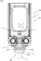
- FIG. 1 shows a sensor housing 1 with a sensor element 2, wherein the sensor housing 1 has an electrical connection 3 with a cable 4 with at least two lines 5 and a first circuit board 6.
- the sensor housing is according to FIG. 1 shown transparently.
- the sensor 28 is an optoelectronic sensor 21.
- FIG. 1a shows a further sensor housing 1 with a sensor element 2, wherein the sensor housing 1 has an electrical connection 3 with a cable 4 with at least two lines 5 and a first circuit board 6.
- resilient contact elements 20 between the contact adapter 7 and the first circuit board 6 is provided.
- the sensor housing is according to FIG. 1a shown transparently.
- the sensor 28 is, for example, an optoelectronic sensor 21.
- FIG. 1a a simple Hotmeltanitati between sensor housing 1 and cable 4 is created. This eliminates a Vorum mousseung. As a result, no O-ring and no locking spring is required.
- the lines 5 are arranged contacted in a contact adapter 7.
- the contact adapter 7 is a second printed circuit board 8 and has metallic contact surfaces 9.
- the contact surfaces 9 are each arranged in different surface portions 22, wherein a first surface portion 23 is connected to the line 5 and the second surface portions 24 of the respective contact surfaces 9 have a common plane plane 11.
- the stripped or non-insulated ends of the lines 5 are thereby inserted through holes or openings of the contact adapter 7 and abut respectively on the first surface portion 23.
- This first surface portion 23 is adapted to the shape of the stripped conductor end and has an approximately semicircular shape with a Lötauge.
- the first surface portion 23 is electrically connected to the second surface portion 24.
- the second surface portion is perpendicular to the first surface portion.
- the conductor ends lie in chamber-like sections of the contact adapter.
- the surface portions 22 are made of copper alloys, for example, and are manufactured in an etching process.
- the main body of the contact adapter consists for example of a thermosetting plastic.
- this planar plane 11 is connected to at least one first end 12 with at least one elastic contact means 14 and a second end 13 of the elastic contact means 14 is connected to the first circuit board 6.
- the contact adapter 7 is automatically soldered to the cables 5 of the cable 4.
- the contact adapter 7 is connected in a placement machine with the lines 5, wherein the line 5 is inserted into the contact adapter 7 or the contact adapter 7 is plugged onto prepositioned lines 5. Subsequently, the contact adapter 7 is automatically soldered to the lines 5, for example by a reflow soldering.
- a contact between the contact adapter 7 and the first circuit board 6 is formed only via a contact contact of the elastic contact means 14.
- the contacting takes place only by the insertion movement along a longitudinal axis of the opening 29 of the sensor housing 1 according to FIG. 1 ,
- the necessary components for connection are placed in the opening 26 of the sensor housing 1.
- the electrical terminal 3 of the sensor housing 1 is mounted after all the components including a windshield are mounted in the sensor housing 1.
- the arrangement of the electrical connection 3 is virtually the last step in the assembly of the sensor 28th
- the cable 4 is inserted with the contact adapter 7 through the opening 26 of the sensor housing 1 from the outside.
- the cable 4 is according to FIG. 3 overmoulded with a plastic compound.
- This plastic compound forms a plastic body 25, which is adapted to the shape of the opening 26 of the sensor housing 1.
- a sealing ring 27 is arranged to form a sealed connection between the plastic body 25 and the sensor housing 1.
- the flat plane 11 of the contact adapter 7 is connected to at least the first end 16 of the elastic contact means 14, as in FIG. 3 shown.
- the elastic contact means 14 is already arranged in the sensor housing interior and connected to the first circuit board 6.
- the sensor housing is in FIG. 3 not shown for better representation of the electrical connection.
- the plastic body 25 After inserting the contact adapter according to FIG. 1 with the cable 4 and the plastic body 25, the plastic body 25 is fixed in the opening 26 of the sensor housing 1.
- an undercut or in each case a recess 30 is provided in the opening 26 of the sensor housing 1 and in the plastic body 25, wherein the undercuts or the recesses 30 face each other.
- the Undercuts or the recess 30 is filled with a potting compound to secure the plastic body 25 in the opening of the sensor housing 1.
- the elastic contact means 14 is an elastic contact body 15 and the flat plane 11 rests on a first plane 16 of the elastic contact body 15 and a second plane 17 of the elastic contact body 15 rests on the first circuit board 6.
- the elastic contact body 15 consists of elastic conductive material per contact section. Between this conductive material elastic insulating body are arranged to separate the individual contact portions. By the elastic contact body 15 a contact is guaranteed even with dimensional tolerances of the mechanical components.
- the elastic contact body has an elastic insulating body 18 and a plurality of respectively insulated conductors 19, the ends of which can be contacted on the first plane and on the second plane, respectively.
- the conductors 19 are formed for example by a plurality of juxtaposed coil springs, ladder tufts or contact springs which are surrounded by an elastic insulating body 18.
- the elastic contact means 14 is formed by resilient contact elements 20.
- the resilient contact elements 20 are formed for example by coil springs or similar spring elements.
- the resilient contact elements 20 are, for example, only spaced apart for insulation, without additional insulation means.
- the resilient contact elements 20 according to FIG. 1 a arranged on the contact adapter 7 and on the first circuit board 6.
- the resilient contact elements 20 can be arranged, for example, directly on the contact surfaces 9 of the plane plane 11.
- the resilient contact elements 20 are connected in one piece or by soldering with the contact surfaces 9.
- the resilient contact elements 20 are then together with the contact adapter 7 in the opening 26 according to FIG. 1 introduced and the resilient contact elements 20 are pressed against the contacts of the first circuit board 6.
- the plastic body is formed by injecting plastic, so-called hot melt, according to FIG. 1a ,
- the contact elements 20 are equipped, for example, by SMD technology on the printed circuit board 6. As a result, they can be cost-effectively positioned in one step in the SMD assembly of the printed circuit board 6 and are better protected during assembly
Landscapes
- Engineering & Computer Science (AREA)
- Physics & Mathematics (AREA)
- General Physics & Mathematics (AREA)
- Manufacturing & Machinery (AREA)
- Microelectronics & Electronic Packaging (AREA)
- Switches Operated By Changes In Physical Conditions (AREA)
Abstract
Description
- Die vorliegende Erfindung betrifft ein Sensorgehäuse nach dem Oberbegriff von Anspruch 1.
- Sensorgehäuse werden nach dem Stand der Technik mit einem Anschlusskabel mit Leitungen verbunden. Dabei wird beispielsweise eine elektronische Baugruppe des Sensors mit dem Kabel bzw. den Leitungen verlötet und dann anschließend in dem Sensorgehäuse angeordnet, wobei das Kabel durch eine Kabelöffnung gefädelt wird. Danach werden weitere Baugruppen in dem Sensorgehäuse angeordnet. Diese Lösungen erfordern eine Montage des Anschlusses bevor die Baugruppen des Sensors montiert werden.
- Weiter ist es beispielsweise nach dem Stand der Technik vorgesehen, dass Anschlüsse an dem Sensorgehäuse von außen auf das Sensorgehäuse aufgesteckt werden und dann beispielsweise mit dem Sensorgehäuse verklebt werden. Diese Lösungen führen zu einer unnötigen Vergrößerung der Außenabmessungen des Sensors.
- Eine Aufgabe der Erfindung besteht darin, einen Sensor bereitzustellen, wobei der Anschluss am Ende der Fertigung des Sensors erfolgen kann, wobei der Anschluss möglichst wenig Platz beanspruchen soll. Weiter sollen die Toleranzanforderungen niedrig sein. Weiter soll eine kostengünstige Anschlussmöglichkeit für Sensoren bereitgestellt werden.
- Die Aufgabe wird gemäß Anspruch 1 gelöst durch ein Sensorgehäuse mit einem Sensorelement, wobei das Sensorgehäuse einen elektrischen Anschluss mit einem Kabel mit mindestens zwei Leitungen und eine erste Leiterplatte aufweist, wobei die Leitungen in einem Kontaktadapter kontaktiert angeordnet sind, wobei der Kontaktadapter eine zweite Leiterplatte ist und metallische Kontaktflächen aufweist, wobei die Kontaktflächen jeweils in unterschiedlichen Flächenabschnitten angeordnet sind, wobei ein erster Flächenabschnitt mit der Leitung verbunden ist und die zweiten Flächenabschnitte der jeweiligen Kontaktflächen eine gemeinsame plane Ebene aufweisen, wobei der zweite Flächenabschnitt rechtwinklig zu dem ersten Flächenabschnitt ist, wobei diese plane Ebene mit mindestens einem ersten Ende mindestens eines elastischen Kontaktmittel verbunden ist und ein zweites Ende des elastischen Kontaktmittels mit der ersten Leiterplatte verbunden ist.
- Gemäß der Erfindung wird ein Kontakt zwischen dem Kontaktadapter und der ersten Leiterplatte nur über einen Berührungskontakt des elastischen Kontaktmittels gebildet. Die Kontaktierung erfolgt dabei lediglich durch die Einführungsbewegung entlang einer Längsachse der Öffnung des Sensorgehäuses. Die Kontaktierung erfolgt damit an einem bereits komplett montierten Sensor mit geschlossenem Sensorgehäuse. Lediglich die Öffnung für den Kontaktadapter ist noch offen.
- Durch das elastische Kontaktmittel ist die Kontaktierung toleranzunempfindlich. Auch bei Temperaturschwankungen wird eine sichere Kontaktierung gewährleistet. Weiter ist die Kontaktierung platzsparend ausgeführt, da die notwendigen Komponenten zum Anschluss in der Öffnung des Sensorgehäuses platziert werden können.
- Weiter kann gemäß der Erfindung der elektrische Anschluss des Sensorgehäuses montiert werden, nachdem alle Komponenten, einschließlich einer Frontscheibe in dem Sensorgehäuse montiert sind. Die Anordnung des elektrischen Anschlusses ist quasi der letzte Arbeitsschritt bei der Montage des Sensors.
- Gemäß der Erfindung kann das Kabel mit dem Kontaktadapter durch eine Öffnung des Sensorgehäuses von außen eingeführt werden. Das Kabel kann dabei optional mit einer Kunststoffmasse umspritzt sein. Diese Kunststoffmasse bildet einen Kunststoffkörper, der an die Form der Öffnung des Gehäuses angepasst ist. Auf dieser Kunststoffmasse kann optional ein Dichtungsring angeordnet sein, um eine dichte Verbindung zwischen dem Kunststoffkörper und dem Sensorgehäuse zu bilden.
- Nach dem Einführen des Kontaktadapters mit dem Kabel wird die plane Ebene des Kontaktadapters mit mindestens dem ersten Ende des elastischen Kontaktmittels verbunden. Das elastische Kontaktmittel ist bereits im Sensorgehäuseinnern angeordnet und mit der ersten Leiterplatte verbunden.
- Nach Einführen des Kontaktadapters mit dem Kabel und dem Kunststoffkörper wird der Kunststoffkörper in der Öffnung des Sensorgehäuses fixiert. Dazu ist beispielsweise in der Öffnung des Sensorgehäuses und in dem Kunststoffkörper jeweils ein Hinterschnitt bzw. jeweils eine Aussparung vorgesehen, wobei sich die Hinterschnitte bzw. die Aussparungen gegenüberstehen. Die Hinterschnitte bzw. die Aussparung werden beispielsweise mit einer Arretierfeder fixiert, oder mit einer Vergussmasse gefüllt, um den Kunststoffkörper in der Öffnung des Sensorgehäuses zu befestigen.
- In Weiterbildung ist das elastische Kontaktmittel ein elastischer Kontaktkörper und die plane Ebene liegt auf einer ersten Ebene des elastischen Kontaktkörpers auf und eine zweite Ebene des elastischen Kontaktkörpers liegt auf der ersten Leiterplatte auf.
- Der elastische Kontaktkörper besteht dabei aus elastischem leitfähigen Material pro Kontaktabschnitt. Zwischen diesem leitfähigen Material sind elastische Isolierkörper angeordnet, um die einzelnen Kontaktabschnitte zu trennen. Durch den elastischen Kontaktkörper ist eine Kontaktierung auch bei Maßtoleranzen der mechanischen Komponenten gewährleistet.
- In einer bevorzugten Ausführungsform der Erfindung weist der elastische Kontaktkörper einen elastischen Isolierkörper auf und eine Vielzahl jeweils isolierter Leiter auf, deren Enden jeweils an der ersten Ebene und an der zweiten Ebene kontaktierbar sind. Die Leiter sind beispielsweise durch eine Vielzahl nebeneinander angeordneter Spiralfedern, Leiterbüschel oder Kontaktfedern gebildet, die von einem elastischen Isolierkörper umgeben sind. Anders formuliert sind eine Vielzahl von parallel beabstandeten flexiblen Leitern in einem elastischen Isolierkörper angeordnet. Dadurch wird quasi eine Leitermatte gebildet, die unabhängig von der Ausrichtung leitende Verbindungen zwischen der planen Ebene des Kontaktadapters und der ersten Leiterplatte bildet.
- Der elastische Kontaktkörper kann auch als Leitermatte bezeichnet werden. Der elastische Kontaktkörper kann beispielsweise auch nur aus Kunststoff/Elastomer bestehen, entscheidend ist die unidirektionale Leitfähigkeit nur in Richtung senkrecht zur Leiterplatten-Ebene.
- In einer weiteren Ausführung kann der Kontaktadapter durch einen anisotrop leitfähigen Klebstoff angeschlossen werden. Die Leitfähigkeit in die gewünschte Richtung entsteht durch eine Anpressung der zu klebenden Bauteile in diese Richtung.
- In Weiterbildung der Erfindung ist das elastische Kontaktmittel durch federnde Kontaktelemente gebildet. Die federnden Kontaktelemente sind beispielsweise durch Spiralfedern oder ähnliche Federelemente gebildet. Die federnden Kontaktelemente sind zur Isolierung beispielsweise lediglich beabstandet angeordnet, ohne zusätzliche Isolierungsmittel.
- In Weiterbildung der Erfindung sind die federnden Kontaktelemente auf dem Kontaktadapter und/oder auf der Leiterplatte angeordnet. Die federnden Kontaktelemente können dabei beispielsweise direkt auf den Kontaktflächen der planen Ebene angeordnet werden. Beispielsweise sind die federnden Kontaktelemente einstückig oder per Lötung mit den Kontaktflächen verbunden. Die federnden Kontaktelemente werden dann zusammen mit dem Kontaktadapter in die Öffnung eingeführt und die federnden Kontaktelemente werden gegen die Kontakte der ersten Leiterplatte gedrückt, wodurch ebenfalls eine robuste toleranzunempfindliche Kontaktierung gebildet wird.
- Es ist jedoch auch vorgesehen, dass die Kontaktelemente beispielsweise per SMD-Technik auf der Leiterplatte bestückt werden. Dadurch können sie kostengünstig in einem Arbeitsschritt bei der SMD-Bestückung der Leiterplatte positioniert werden und sind bei der Montage besser geschützt.
- In Weiterbildung der Erfindung ist der Kontaktadapter automatisiert mit den Leitungen des Kabels verlötbar. Dabei wird der Kontaktadapter in einer Bestückungsmaschine mit den Leitungen verbunden, wobei die Leitungen in den Kontaktadapter gesteckt werden oder der Kontaktadapter auf vorpositionierte Leitungen aufgesteckt wird. Anschließend wird der Kontaktadapter automatisiert mit den Leitungen verlötet, beispielsweise durch Reflow-Lötung. Dadurch ist eine kostengünstige Herstellung möglich.
- Optional kann auch der Kontaktadapter mit der verbundenen Leitung automatisiert in die Öffnung des Sensorgehäuses eingeführt werden und befestigt werden. Hierzu ist beispielsweise eine Montagemaschine vorgesehen. Dabei werden die Kontaktadapter und die Sensorgehäuse gegenüberliegend positioniert und anschließend lediglich der Kontaktadapter mit dem Kabel in die Öffnung in einer linearen Bewegung in das Sensorgehäuse eingeschoben und anschließend fixiert. Dadurch kann quasi der gesamte Sensor automatisiert hergestellt werden, ohne dass manuelle Montageschritte notwendig sind. Lediglich das Bereitstellen der Ausgangskomponenten an der Maschine kann beispielsweise manuell erfolgen.
- In Weiterbildung der Erfindung ist ein Sensor ein optoelektronischer Sensor. Bei dem optoelektronischen Sensor kann es sich beispielsweise um eine Lichtschranke, einen Lichttaster, einen Distanzsensor, eine Reflexionslichtschranke, ein Lichtgitter oder ähnliches handeln. Derartige Sensoren weisen mindestens ein Sendeelement und mindestens ein Empfangselement auf. Die empfangenen Signale des Empfangselements werden von eine Auswerteeinheit ausgewertet und daraufhin wird ein Objektfeststellungssignal ausgegeben. Das Objektfeststellungssignal wird beispielsweise über die Leitungen einer externen Steuerung zugeführt.
- Jedoch kann es sich bei dem Sensor auch um einen induktiven, magnetischen oder kapazitiven Sensor handeln. Weiter kann der Sensor auch ein Ultraschallsensor sein.
- Die Erfindung wird nachstehend auch hinsichtlich weiterer Vorteile und Merkmale unter Bezugnahme auf die beigefügte Zeichnung anhand von Ausführungsbeispielen erläutert. Die Figuren der Zeichnung zeigen in:
- Figur 1
- ein Sensorgehäuse mit einem elektrischen Anschluss;
- Figur 1a
- ein Sensorgehäuse mit einem elektrischen Anschluss;
- Figur 2
- einen Kontaktadapter mit einem Kabel und Leitungen;
- Figur 3
- einen Kontaktadapter mit einem elastischen Kontaktkörper und einer Leiterplatte;
- Figur 4
- einen Kontaktadapter mit einem elastischen Isolierkörper und Leitern;
- Figur 5
- einen Kontaktadapter mit federnden Kontaktelementen.
- In den nachfolgenden Figuren sind identische Teile mit identischen Bezugszeichen versehen.
-
Figur 1 zeigt ein Sensorgehäuse 1 mit einem Sensorelement 2, wobei das Sensorgehäuse 1 einen elektrischen Anschluss 3 mit einem Kabel 4 mit mindestens zwei Leitungen 5 und eine erste Leiterplatte 6 aufweist. Das Sensorgehäuse ist gemäßFigur 1 transparent dargestellt. GemäßFigur 1 ist der Sensor 28 beispielsweise ein optoelektronischer Sensor 21. -
Figur 1a zeigt ein weiteres Sensorgehäuse 1 mit einem Sensorelement 2, wobei das Sensorgehäuse 1 einen elektrischen Anschluss 3 mit einem Kabel 4 mit mindestens zwei Leitungen 5 und eine erste Leiterplatte 6 aufweist. GemäßFigur 1a sind federnde Kontaktelemente 20 zwischen dem Kontaktadapter 7 und der ersten Leiterplatte 6 vorgesehen. Das Sensorgehäuse ist gemäßFigur 1a transparent dargestellt. Gemäß Figur 1a ist der Sensor 28 beispielsweise ein optoelektronischer Sensor 21. - Gemäß
Figur 1a ist eine einfache Hotmeltanbindung zwischen Sensorgehäuse 1 und Kabel 4 angelegt. Dadurch entfällt eine Vorumspritzung. Dadurch ist auch kein O-Ring und keine Arretierfeder erforderlich. - Gemäß
Figur 2 sind die Leitungen 5 in einem Kontaktadapter 7 kontaktiert angeordnet. Der Kontaktadapter 7 ist eine zweite Leiterplatte 8 und weist metallische Kontaktflächen 9 auf. Die Kontaktflächen 9 sind jeweils in unterschiedlichen Flächenabschnitten 22 angeordnet, wobei ein erster Flächenabschnitt 23 mit der Leitung 5 verbunden ist und die zweiten Flächenabschnitte 24 der jeweiligen Kontaktflächen 9 eine gemeinsame plane Ebene 11 aufweisen. - Gemäß
Figur 2 sind die abisolierten bzw. nicht isolierten Enden der Leitungen 5 dabei durch Löcher oder Öffnungen des Kontaktadapters 7 hindurchgesteckt und liegen an jeweils dem ersten Flächenabschnitt 23 an. Dieser erste Flächenabschnitt 23 ist an die Form des abisolierten Leiterendes angepasst und weist eine etwa halbrunde Form mit einem Lötauge auf. Der erste Flächenabschnitt 23 ist mit dem zweiten Flächenabschnitt 24 elektrisch verbunden. Der zweite Flächenabschnitt befindet sich rechtwinklig zu dem ersten Flächenabschnitt. Die Leiterenden liegen in kammerartigen Abschnitten des Kontaktadapters. Die Flächenabschnitte 22 sind beispielsweise aus Kupferlegierungen hergestellt und werden in einem Ätzverfahren hergestellt. Der Grundkörper des Kontaktadapters besteht beispielsweise aus einem Duroplast. - Gemäß
Figur 3 undFigur 1 ist diese plane Ebene 11 mit mindestens einem ersten Ende 12 mit mindestens einem elastischen Kontaktmittel 14 verbunden und ein zweites Ende 13 des elastischen Kontaktmittels 14 ist mit der ersten Leiterplatte 6 verbunden. - Gemäß
Figur 2 ist der Kontaktadapter 7 automatisiert mit den Leitungen 5 des Kabels 4 verlötet. Dabei wird der Kontaktadapter 7 in einer Bestückungsmaschine mit den Leitungen 5 verbunden, wobei die Leitung 5 in den Kontaktadapter 7 gesteckt wird oder der Kontaktadapter 7 auf vorpositionierte Leitungen 5 aufgesteckt wird. Anschließend wird der Kontaktadapter 7 automatisiert mit den Leitungen 5 verlötet, beispielsweise durch eine Reflow-Lötung. - Gemäß
Figur 3 wird ein Kontakt zwischen dem Kontaktadapter 7 und der ersten Leiterplatte 6 nur über einen Berührungskontakt des elastischen Kontaktmittels 14 gebildet. Die Kontaktierung erfolgt dabei lediglich durch die Einführungsbewegung entlang einer Längsachse der Öffnung 29 des Sensorgehäuses 1 gemäßFigur 1 . - Die notwendigen Komponenten zum Anschluss sind in der Öffnung 26 des Sensorgehäuses 1 platziert.
- Gemäß
Figur 1 wird der elektrische Anschluss 3 des Sensorgehäuses 1 montiert, nachdem alle Komponenten, einschließlich einer Frontscheibe, in dem Sensorgehäuse 1 montiert sind. Die Anordnung des elektrischen Anschlusses 3 ist quasi der letzte Arbeitsschritt bei der Montage des Sensors 28. - Gemäß
Figur 1 wird das Kabel 4 mit dem Kontaktadapter 7 durch die Öffnung 26 des Sensorgehäuses 1 von außen eingeführt. Das Kabel 4 ist dabei gemäßFigur 3 mit einer Kunststoffmasse umspritzt. Diese Kunststoffmasse bildet einen Kunststoffkörper 25, der an die Form der Öffnung 26 des Sensorgehäuses 1 angepasst ist. Auf dieser Kunststoffmasse ist ein Dichtungsring 27 angeordnet, um eine dichte Verbindung zwischen dem Kunststoffkörper 25 und dem Sensorgehäuse 1 zu bilden. - Nach dem Einführen des Kontaktadapters 7 mit dem Kabel 4 wird die plane Ebene 11 des Kontaktadapters 7 mit mindestens dem ersten Ende 16 des elastischen Kontaktmittels 14 verbunden, wie in
Figur 3 dargestellt. Das elastische Kontaktmittel 14 ist bereits im Sensorgehäuseinnern angeordnet und mit der ersten Leiterplatte 6 verbunden. Das Sensorgehäuse ist inFigur 3 zur besseren Darstellung des elektrischen Anschlusses nicht dargestellt. - Nach Einführen des Kontaktadapters gemäß
Figur 1 mit dem Kabel 4 und dem Kunststoffkörper 25, wird der Kunststoffkörper 25 in der Öffnung 26 des Sensorgehäuses 1 fixiert. Dazu ist beispielsweise in der Öffnung 26 des Sensorgehäuses 1 und in dem Kunststoffkörper 25 jeweils ein Hinterschnitt bzw. jeweils eine Aussparung 30 vorgesehen, wobei sich die Hinterschnitte bzw. die Aussparungen 30 gegenüberstehen. Die Hinterschnitte bzw. die Aussparung 30 wird mit einer Vergussmasse gefüllt, um den Kunststoffkörper 25 in der Öffnung des Sensorgehäuses 1 zu befestigen. - Gemäß
Figur 3 ist das elastische Kontaktmittel 14 ein elastischer Kontaktkörper 15 und die plane Ebene 11 liegt auf einer ersten Ebene 16 des elastischen Kontaktkörpers 15 auf und eine zweite Ebene 17 des elastischen Kontaktkörpers 15 liegt auf der ersten Leiterplatte 6 auf. - Der elastische Kontaktkörper 15 besteht dabei aus elastischem leitfähigen Material pro Kontaktabschnitt. Zwischen diesem leitfähigen Material sind elastische Isolierkörper angeordnet, um die einzelnen Kontaktabschnitte zu trennen. Durch den elastischen Kontaktkörper 15 ist eine Kontaktierung auch bei Maßtoleranzen der mechanischen Komponenten gewährleistet.
- Gemäß
Figur 4 weist der elastische Kontaktkörper einen elastischen Isolierkörper 18 und eine Vielzahl jeweils isolierter Leiter 19 auf, deren Enden jeweils an der ersten Ebene und an der zweiten Ebene kontaktierbar sind. Die Leiter 19 sind beispielsweise durch eine Vielzahl nebeneinander angeordneter Spiralfedern, Leiterbüschel oder Kontaktfedern gebildet die von einem elastischen Isolierkörper 18 umgeben sind. - Gemäß
Figur 5 ist das elastische Kontaktmittel 14 durch federnde Kontaktelemente 20 gebildet. Die federnden Kontaktelemente 20 sind beispielsweise durch Spiralfedern oder ähnliche Federelemente gebildet. Die federnden Kontaktelemente 20 sind zur Isolierung beispielsweise lediglich beabstandet angeordnet, ohne zusätzliche Isolierungsmittel. - Gemäß
Figur 5 sind die federnden Kontaktelemente 20 gemäßFigur 1 a auf dem Kontaktadapter 7 bzw. auf der ersten Leiterplatte 6 angeordnet. Die federnden Kontaktelemente 20 können dabei beispielsweise direkt auf den Kontaktflächen 9 der planen Ebene 11 angeordnet werden. Beispielsweise sind die federnden Kontaktelemente 20 einstückig oder per Lötung mit den Kontaktflächen 9 verbunden. Die federnden Kontaktelemente 20 werden dann zusammen mit dem Kontaktadapter 7 in die Öffnung 26 gemäßFigur 1 eingeführt und die federnden Kontaktelemente 20 werden gegen die Kontakte der ersten Leiterplatte 6 gedrückt. Der Kunststoffkörper ist durch Einspritzen von Kunststoff, sog. Hotmelt, gebildet, entsprechend zuFigur 1a . - Es ist jedoch auch vorgesehen, dass die Kontaktelemente 20 beispielsweise per SMD-Technik auf der Leiterplatte 6 bestückt werden. Dadurch können sie kostengünstig, in einem Arbeitsschritt bei der SMD-Bestückung der Leiterplatte 6 positioniert werden und sind bei der Montage besser geschützt
-
- 1
- Sensorgehäuse
- 2
- Sensorelement
- 3
- elektrischer Anschluss
- 4
- Kabel
- 5
- Leitungen
- 6
- erste Leiterplatte
- 7
- Kontaktadapter
- 8
- zweite Leiterplatte
- 9
- Kontaktflächen
- 11
- plane Ebene
- 12
- erstes Ende
- 13
- zweites Ende
- 14
- elastisches Kontaktmittel
- 15
- elastischer Kontaktkörper
- 16
- erste Ebene
- 17
- zweite Ebene
- 18
- elastischer Isolierkörper
- 19
- isolierter Leiter
- 20
- federnde Kontaktelemente
- 21
- optoelektronischer Sensor
- 22
- Flächenabschnitte
- 23
- erster Flächenabschnitt
- 24
- zweiter Flächenabschnitt
- 25
- Kunststoffkörper
- 26
- Öffnung
- 27
- Dichtungsring
- 28
- Sensor
- 30
- Aussparung
Claims (7)
- Sensorgehäuse mit einem Sensorelement (2), wobei das Sensorgehäuse (1) einen elektrischen Anschluss (3) mit einem Kabel (4) mit mindestens zwei Leitungen (5) und eine erste Leiterplatte (6) aufweist,
dadurch gekennzeichnet, dass
die Leitungen (5) in einem Kontaktadapter (7) kontaktiert angeordnet sind, wobei der Kontaktadapter (7) eine zweite Leiterplatte (8) ist und metallische Kontaktflächen (9) aufweist,
wobei die Kontaktflächen (9) jeweils in unterschiedlichen Flächenabschnitten (22) angeordnet sind,
wobei ein erster Flächenabschnitt (23) mit der Leitung verbunden ist und die zweiten Flächenabschnitte (24) der jeweiligen Kontaktflächen (9) eine gemeinsame plane Ebene (11) aufweisen,
wobei der zweite Flächenabschnitt rechtwinklig zu dem ersten Flächenabschnitt ist,
wobei diese plane Ebene (11) mit mindestens einem ersten Ende (12) mindestens eines elastischen Kontaktmittels (14) verbunden ist und ein zweites Ende (13) des elastischen Kontaktmittels (14) mit der ersten Leiterplatte (6) verbunden ist. - Sensorgehäuse nach Anspruch 1, dadurch gekennzeichnet, dass das elastische Kontaktmittel (14) ein elastischer Kontaktkörper (15) ist und die plane Ebene (11) auf einer ersten Ebene (16) des elastischen Kontaktkörpers (15) aufliegt und eine zweite Ebene (17) des elastischen Kontaktkörpers (15) auf der ersten Leiterplatte (6) aufliegt.
- Sensorgehäuse nach Anspruch 2, dadurch gekennzeichnet, dass der elastische Kontaktkörper (15) einen elastischen Isolierkörper (18) aufweist und eine Vielzahl jeweils isolierter Leiter (19) aufweist, deren Enden jeweils an der ersten Ebene (16) und an der zweiten Ebene (17) kontaktierbar sind.
- Sensorgehäuse nach Anspruch 1, dadurch gekennzeichnet, dass das elastische Kontaktmittel (14) durch federnde Kontaktelemente (20) gebildet ist.
- Sensorgehäuse nach Anspruch 4, dadurch gekennzeichnet, dass die federnden Kontaktelemente (20) auf dem Kontaktadapter (7) und/oder auf der Leiterplatte (6) angeordnet sind.
- Sensorgehäuse nach mindestens einem der vorhergehenden Ansprüche, dadurch gekennzeichnet, dass der Kontaktadapter (7) automatisiert mit den Leitungen (5) des Kabels (4) verlötbar ist.
- Sensorgehäuse nach mindestens einem der vorhergehenden Ansprüche, dadurch gekennzeichnet, dass ein Sensor (28) ein optoelektronischer Sensor (21) ist.
Applications Claiming Priority (1)
| Application Number | Priority Date | Filing Date | Title |
|---|---|---|---|
| DE102016110466.3A DE102016110466B3 (de) | 2016-06-07 | 2016-06-07 | Sensorgehäuse |
Publications (1)
| Publication Number | Publication Date |
|---|---|
| EP3255387A1 true EP3255387A1 (de) | 2017-12-13 |
Family
ID=58745081
Family Applications (1)
| Application Number | Title | Priority Date | Filing Date |
|---|---|---|---|
| EP17171698.8A Withdrawn EP3255387A1 (de) | 2016-06-07 | 2017-05-18 | Sensorgehäuse |
Country Status (2)
| Country | Link |
|---|---|
| EP (1) | EP3255387A1 (de) |
| DE (1) | DE102016110466B3 (de) |
Citations (4)
| Publication number | Priority date | Publication date | Assignee | Title |
|---|---|---|---|---|
| DE102007017917A1 (de) * | 2007-04-13 | 2008-10-23 | Sick Ag | Funktionseinheit für einen optoelektronischen Sensor und Verfahren zur Anbringung einer Leiterplatte |
| DE102008059661A1 (de) * | 2008-11-28 | 2010-06-10 | Sensopart Industriesensorik Gmbh | Optischer Sensor |
| DE102011119842A1 (de) * | 2011-12-01 | 2013-06-06 | I F M Electronic Gmbh | Elektrisches Verbindungselement und Leiterplattenanordnung |
| DE102014114569A1 (de) * | 2014-10-08 | 2016-04-14 | Connaught Electronics Ltd. | Kamera für ein Kraftfahrzeug mit einer Haltevorrichtung |
Family Cites Families (3)
| Publication number | Priority date | Publication date | Assignee | Title |
|---|---|---|---|---|
| DE4434011C1 (de) * | 1994-09-23 | 1995-07-20 | Leuze Electronic Gmbh & Co | Optoelektronische Vorrichtung |
| DE10234466B4 (de) * | 2002-07-29 | 2006-07-27 | Siemens Ag | Optoelektronisches Gerät zur optischen Erfassung eines Objekts |
| US20090095074A1 (en) * | 2007-10-12 | 2009-04-16 | Yevgeniy Vinshtok | Sensor housing |
-
2016
- 2016-06-07 DE DE102016110466.3A patent/DE102016110466B3/de active Active
-
2017
- 2017-05-18 EP EP17171698.8A patent/EP3255387A1/de not_active Withdrawn
Patent Citations (4)
| Publication number | Priority date | Publication date | Assignee | Title |
|---|---|---|---|---|
| DE102007017917A1 (de) * | 2007-04-13 | 2008-10-23 | Sick Ag | Funktionseinheit für einen optoelektronischen Sensor und Verfahren zur Anbringung einer Leiterplatte |
| DE102008059661A1 (de) * | 2008-11-28 | 2010-06-10 | Sensopart Industriesensorik Gmbh | Optischer Sensor |
| DE102011119842A1 (de) * | 2011-12-01 | 2013-06-06 | I F M Electronic Gmbh | Elektrisches Verbindungselement und Leiterplattenanordnung |
| DE102014114569A1 (de) * | 2014-10-08 | 2016-04-14 | Connaught Electronics Ltd. | Kamera für ein Kraftfahrzeug mit einer Haltevorrichtung |
Also Published As
| Publication number | Publication date |
|---|---|
| DE102016110466B3 (de) | 2017-10-12 |
Similar Documents
| Publication | Publication Date | Title |
|---|---|---|
| DE102008059477B4 (de) | Elektrischer Mehrfachverteiler | |
| DE102013101823B4 (de) | Kontaktträger mit einem Unterteil | |
| WO2015044068A1 (de) | Steckverbinderteil mit einer widerstandkodierung | |
| DE102012218847A1 (de) | Anschlusselement für eine Antriebsanordnung sowie eine Antriebsanordnung mit einem Anschlussteil | |
| EP1972039B1 (de) | Anschlussadapter für sensoren oder aktuatoren | |
| EP2277242B1 (de) | Messerleisten-kontaktierung über zwischenleiterplatten | |
| WO2007113030A1 (de) | Anschlussmodul zum anschluss einer steuereinheit oder dergleichen an eine antriebseinheit | |
| EP2997645A2 (de) | Kontaktierungskomponente für ein antriebsmodul, antriebsmodul sowie verfahren zur herstellung einer kontaktierungskomponente | |
| DE102018104843A1 (de) | Erdungsanschlusselement zur Abschirmung von in Kunststoffgehäusen angeordneten elektrischen Komponenten sowie Verfahren zu seinem Einbau | |
| DE102008059661B4 (de) | Optischer Sensor | |
| WO2015107188A2 (de) | Elektronikbaugruppe | |
| DE202016103012U1 (de) | Sensorgehäuse | |
| DE19858534A1 (de) | Elektrischer Verbinder | |
| EP3610539A1 (de) | Elektrische kontaktanordnung | |
| DE19804607C2 (de) | Anordnung zum elektrischen Anschluß zumindest eines Sensors | |
| DE102016110466B3 (de) | Sensorgehäuse | |
| EP2673848A1 (de) | Steckverbindung zur elektrischen direktkontaktierung einer leiterplatte | |
| DE102012221603A1 (de) | Stellantriebsanordnung | |
| DE10161102A1 (de) | Leitungs-Steckverbindung für elektrisches Steuergerät sowie Herstellungsverfahren | |
| DE102017203142B4 (de) | Verkettungsmodul | |
| EP2274803A1 (de) | Steckverbinder | |
| DE102006009582B4 (de) | Elektronisches Gerät eines Fahrzeuges, insbesondere ein Antennenverstärker oder ein TV-Tuner, mit einem Aufnahmeraum für einen Steckverbinder | |
| WO2006048233A1 (de) | Batteriestromsensor für ein kraftfahrzeug | |
| DE102010039957B4 (de) | Trennbuchsenanordnungen und Trennadapter mit einer Trägerplatte und einer oder mehreren darin angebrachten Trennbuchsen der Trennbuchsenanordnungen | |
| EP1988609A2 (de) | Steckverbindung für Schaltungsträger |
Legal Events
| Date | Code | Title | Description |
|---|---|---|---|
| PUAI | Public reference made under article 153(3) epc to a published international application that has entered the european phase |
Free format text: ORIGINAL CODE: 0009012 |
|
| AK | Designated contracting states |
Kind code of ref document: A1 Designated state(s): AL AT BE BG CH CY CZ DE DK EE ES FI FR GB GR HR HU IE IS IT LI LT LU LV MC MK MT NL NO PL PT RO RS SE SI SK SM TR |
|
| AX | Request for extension of the european patent |
Extension state: BA ME |
|
| STAA | Information on the status of an ep patent application or granted ep patent |
Free format text: STATUS: THE APPLICATION HAS BEEN WITHDRAWN |
|
| 17P | Request for examination filed |
Effective date: 20180613 |
|
| RBV | Designated contracting states (corrected) |
Designated state(s): AL AT BE BG CH CY CZ DE DK EE ES FI FR GB GR HR HU IE IS IT LI LT LU LV MC MK MT NL NO PL PT RO RS SE SI SK SM TR |
|
| 18W | Application withdrawn |
Effective date: 20180704 |