EP3252829A1 - Organic semiconductor element - Google Patents
Organic semiconductor element Download PDFInfo
- Publication number
- EP3252829A1 EP3252829A1 EP16743394.5A EP16743394A EP3252829A1 EP 3252829 A1 EP3252829 A1 EP 3252829A1 EP 16743394 A EP16743394 A EP 16743394A EP 3252829 A1 EP3252829 A1 EP 3252829A1
- Authority
- EP
- European Patent Office
- Prior art keywords
- organic semiconductor
- strain
- semiconductor element
- semiconductor layer
- given
- Prior art date
- Legal status (The legal status is an assumption and is not a legal conclusion. Google has not performed a legal analysis and makes no representation as to the accuracy of the status listed.)
- Pending
Links
Images

Classifications
-
- G—PHYSICS
- G01—MEASURING; TESTING
- G01L—MEASURING FORCE, STRESS, TORQUE, WORK, MECHANICAL POWER, MECHANICAL EFFICIENCY, OR FLUID PRESSURE
- G01L1/00—Measuring force or stress, in general
- G01L1/18—Measuring force or stress, in general using properties of piezo-resistive materials, i.e. materials of which the ohmic resistance varies according to changes in magnitude or direction of force applied to the material
-
- H—ELECTRICITY
- H10—SEMICONDUCTOR DEVICES; ELECTRIC SOLID-STATE DEVICES NOT OTHERWISE PROVIDED FOR
- H10D—INORGANIC ELECTRIC SEMICONDUCTOR DEVICES
- H10D30/00—Field-effect transistors [FET]
- H10D30/60—Insulated-gate field-effect transistors [IGFET]
- H10D30/67—Thin-film transistors [TFT]
-
- H—ELECTRICITY
- H10—SEMICONDUCTOR DEVICES; ELECTRIC SOLID-STATE DEVICES NOT OTHERWISE PROVIDED FOR
- H10D—INORGANIC ELECTRIC SEMICONDUCTOR DEVICES
- H10D48/00—Individual devices not covered by groups H10D1/00 - H10D44/00
- H10D48/50—Devices controlled by mechanical forces, e.g. pressure
-
- H—ELECTRICITY
- H10—SEMICONDUCTOR DEVICES; ELECTRIC SOLID-STATE DEVICES NOT OTHERWISE PROVIDED FOR
- H10K—ORGANIC ELECTRIC SOLID-STATE DEVICES
- H10K10/00—Organic devices specially adapted for rectifying, amplifying, oscillating or switching; Organic capacitors or resistors having potential barriers
-
- H—ELECTRICITY
- H10—SEMICONDUCTOR DEVICES; ELECTRIC SOLID-STATE DEVICES NOT OTHERWISE PROVIDED FOR
- H10K—ORGANIC ELECTRIC SOLID-STATE DEVICES
- H10K10/00—Organic devices specially adapted for rectifying, amplifying, oscillating or switching; Organic capacitors or resistors having potential barriers
- H10K10/40—Organic transistors
-
- H—ELECTRICITY
- H10—SEMICONDUCTOR DEVICES; ELECTRIC SOLID-STATE DEVICES NOT OTHERWISE PROVIDED FOR
- H10K—ORGANIC ELECTRIC SOLID-STATE DEVICES
- H10K10/00—Organic devices specially adapted for rectifying, amplifying, oscillating or switching; Organic capacitors or resistors having potential barriers
- H10K10/40—Organic transistors
- H10K10/46—Field-effect transistors, e.g. organic thin-film transistors [OTFT]
- H10K10/462—Insulated gate field-effect transistors [IGFETs]
- H10K10/466—Lateral bottom-gate IGFETs comprising only a single gate
-
- H—ELECTRICITY
- H10—SEMICONDUCTOR DEVICES; ELECTRIC SOLID-STATE DEVICES NOT OTHERWISE PROVIDED FOR
- H10K—ORGANIC ELECTRIC SOLID-STATE DEVICES
- H10K10/00—Organic devices specially adapted for rectifying, amplifying, oscillating or switching; Organic capacitors or resistors having potential barriers
- H10K10/40—Organic transistors
- H10K10/46—Field-effect transistors, e.g. organic thin-film transistors [OTFT]
- H10K10/462—Insulated gate field-effect transistors [IGFETs]
- H10K10/484—Insulated gate field-effect transistors [IGFETs] characterised by the channel regions
- H10K10/488—Insulated gate field-effect transistors [IGFETs] characterised by the channel regions the channel region comprising a layer of composite material having interpenetrating or embedded materials, e.g. a mixture of donor and acceptor moieties, that form a bulk heterojunction
-
- H—ELECTRICITY
- H10—SEMICONDUCTOR DEVICES; ELECTRIC SOLID-STATE DEVICES NOT OTHERWISE PROVIDED FOR
- H10K—ORGANIC ELECTRIC SOLID-STATE DEVICES
- H10K71/00—Manufacture or treatment specially adapted for the organic devices covered by this subclass
- H10K71/10—Deposition of organic active material
- H10K71/12—Deposition of organic active material using liquid deposition, e.g. spin coating
-
- H—ELECTRICITY
- H10—SEMICONDUCTOR DEVICES; ELECTRIC SOLID-STATE DEVICES NOT OTHERWISE PROVIDED FOR
- H10K—ORGANIC ELECTRIC SOLID-STATE DEVICES
- H10K71/00—Manufacture or treatment specially adapted for the organic devices covered by this subclass
- H10K71/10—Deposition of organic active material
- H10K71/12—Deposition of organic active material using liquid deposition, e.g. spin coating
- H10K71/15—Deposition of organic active material using liquid deposition, e.g. spin coating characterised by the solvent used
-
- H—ELECTRICITY
- H10—SEMICONDUCTOR DEVICES; ELECTRIC SOLID-STATE DEVICES NOT OTHERWISE PROVIDED FOR
- H10K—ORGANIC ELECTRIC SOLID-STATE DEVICES
- H10K85/00—Organic materials used in the body or electrodes of devices covered by this subclass
- H10K85/60—Organic compounds having low molecular weight
- H10K85/615—Polycyclic condensed aromatic hydrocarbons, e.g. anthracene
- H10K85/622—Polycyclic condensed aromatic hydrocarbons, e.g. anthracene containing four rings, e.g. pyrene
-
- H—ELECTRICITY
- H10—SEMICONDUCTOR DEVICES; ELECTRIC SOLID-STATE DEVICES NOT OTHERWISE PROVIDED FOR
- H10K—ORGANIC ELECTRIC SOLID-STATE DEVICES
- H10K85/00—Organic materials used in the body or electrodes of devices covered by this subclass
- H10K85/60—Organic compounds having low molecular weight
- H10K85/615—Polycyclic condensed aromatic hydrocarbons, e.g. anthracene
- H10K85/623—Polycyclic condensed aromatic hydrocarbons, e.g. anthracene containing five rings, e.g. pentacene
-
- H—ELECTRICITY
- H10—SEMICONDUCTOR DEVICES; ELECTRIC SOLID-STATE DEVICES NOT OTHERWISE PROVIDED FOR
- H10K—ORGANIC ELECTRIC SOLID-STATE DEVICES
- H10K85/00—Organic materials used in the body or electrodes of devices covered by this subclass
- H10K85/60—Organic compounds having low molecular weight
- H10K85/649—Aromatic compounds comprising a hetero atom
- H10K85/657—Polycyclic condensed heteroaromatic hydrocarbons
- H10K85/6574—Polycyclic condensed heteroaromatic hydrocarbons comprising only oxygen in the heteroaromatic polycondensed ring system, e.g. cumarine dyes
-
- H—ELECTRICITY
- H10—SEMICONDUCTOR DEVICES; ELECTRIC SOLID-STATE DEVICES NOT OTHERWISE PROVIDED FOR
- H10K—ORGANIC ELECTRIC SOLID-STATE DEVICES
- H10K85/00—Organic materials used in the body or electrodes of devices covered by this subclass
- H10K85/60—Organic compounds having low molecular weight
- H10K85/649—Aromatic compounds comprising a hetero atom
- H10K85/657—Polycyclic condensed heteroaromatic hydrocarbons
- H10K85/6576—Polycyclic condensed heteroaromatic hydrocarbons comprising only sulfur in the heteroaromatic polycondensed ring system, e.g. benzothiophene
-
- G—PHYSICS
- G01—MEASURING; TESTING
- G01B—MEASURING LENGTH, THICKNESS OR SIMILAR LINEAR DIMENSIONS; MEASURING ANGLES; MEASURING AREAS; MEASURING IRREGULARITIES OF SURFACES OR CONTOURS
- G01B7/00—Measuring arrangements characterised by the use of electric or magnetic techniques
- G01B7/16—Measuring arrangements characterised by the use of electric or magnetic techniques for measuring the deformation in a solid, e.g. by resistance strain gauge
-
- H—ELECTRICITY
- H10—SEMICONDUCTOR DEVICES; ELECTRIC SOLID-STATE DEVICES NOT OTHERWISE PROVIDED FOR
- H10K—ORGANIC ELECTRIC SOLID-STATE DEVICES
- H10K77/00—Constructional details of devices covered by this subclass and not covered by groups H10K10/80, H10K30/80, H10K50/80 or H10K59/80
- H10K77/10—Substrates, e.g. flexible substrates
- H10K77/111—Flexible substrates
-
- Y—GENERAL TAGGING OF NEW TECHNOLOGICAL DEVELOPMENTS; GENERAL TAGGING OF CROSS-SECTIONAL TECHNOLOGIES SPANNING OVER SEVERAL SECTIONS OF THE IPC; TECHNICAL SUBJECTS COVERED BY FORMER USPC CROSS-REFERENCE ART COLLECTIONS [XRACs] AND DIGESTS
- Y02—TECHNOLOGIES OR APPLICATIONS FOR MITIGATION OR ADAPTATION AGAINST CLIMATE CHANGE
- Y02E—REDUCTION OF GREENHOUSE GAS [GHG] EMISSIONS, RELATED TO ENERGY GENERATION, TRANSMISSION OR DISTRIBUTION
- Y02E10/00—Energy generation through renewable energy sources
- Y02E10/50—Photovoltaic [PV] energy
- Y02E10/549—Organic PV cells
Definitions
- the present invention relates to an organic semiconductor element.
- an organic semiconductor element of this type there has been proposed an organic semiconductor element in which a compressive stress is applied to a multi-crystal or amorphous organic semiconductor (see Patent Literature 1, for example).
- the organic semiconductor is formed as a thin film on a bent substrate by a vapor deposition or a spin coating, and the compressive stress is applied to the organic semiconductor by stretching the bent substrate until the substrate becomes planar.
- the compressive stress applied to the organic semiconductor With the compressive stress applied to the organic semiconductor, the carrier mobility of the organic semiconductor is increased.
- organic semiconductor element since a multi-crystal or amorphous organic semiconductor is used, it is difficult to obtain organic semiconductors having an identical multi-crystal structure or an identical amorphous structure. Because of the difference in the structure, even when organic semiconductors are produced by the same technique and the same compressive stress is applied so that the same strain is given, the organic semiconductors often differ in the carrier mobility, and it is difficult to obtain organic semiconductor elements having uniform property.
- a primary object of an organic semiconductor element in the present invention is to provide organic semiconductor elements having uniform property.
- an organic semiconductor element in the present invention adopts the following configurations.
- the organic semiconductor element includes an organic semiconductor.
- the organic semiconductor is formed as a single-crystal thin film, and the organic semiconductor element operates based on carrier mobility when a strain is given to at least the organic semiconductor.
- the organic semiconductor is formed as the single-crystal thin film.
- the crystal structure of a single crystal is determined by the molecules, and therefore, basically, an identical crystal structure is obtained regardless of the production technique. Therefore, when the same strain is given, the same carrier mobility can be obtained. Accordingly, it is possible to obtain organic semiconductor elements having uniform property.
- the organic semiconductor may be formed as a thin film whose thickness is 200 nm or less, for example, 100 nm or 50 nm. It is preferable that the strain to be given to the organic semiconductor be in a range of 10% or less in a compression direction. Further, as the organic semiconductor, the organic semiconductor may be composed of a polycyclic aromatic compound with four or more rings, or a polycyclic compound with four or more rings including at least one unsaturated five-membered heterocyclic compound and a plurality of benzene rings.
- the organic semiconductor may be kept in a state where a predetermined strain is applied in a movement direction of carriers. That is, the organic semiconductor is used while the carrier mobility is fixed in the state where the predetermined strain is applied.
- the organic semiconductor By using such an organic semiconductor, it is possible to obtain various semiconductor devices.
- the organic semiconductor element may be operated based on mobility of carriers when a predetermined strain as a standard is given to the organic semiconductor and carrier mobility when a different strain from the predetermined strain is given to the organic semiconductor. Thereby, it is possible to use the organic semiconductor element as a sensor device.
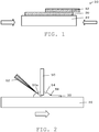
- FIG 1 is an explanatory diagram showing an exemplary configuration of an organic semiconductor element 20 that functions as a strain sensor according to a first embodiment of the present invention.
- the organic semiconductor element 20 includes a substrate 22, an organic semiconductor layer 30 formed on the substrate 22, and two gauge leads 32 formed on the organic semiconductor layer 30 (one of the two gauge leads 32 is not illustrated).
- the substrate 22 is formed of a plastic (for example, polyethylene naphthalate), such that the thickness is 50 ⁇ m to 10 mm, for example, 100 ⁇ m to 200 ⁇ m.
- a plastic for example, polyethylene naphthalate
- the organic semiconductor layer 30 is formed such that the thickness is 200 nm or less, for example, 100 nm or 50 nm, as a single-crystal thin film of an organic semiconductor (for example, 3,11-didecyldinaphto [2,3-d:2',3'-d']benzo [1,2-b:4,5-b']dithiophene (C10-DNBDT) having a structure shown in the following Formula (1)).
- an organic semiconductor for example, 3,11-didecyldinaphto [2,3-d:2',3'-d']benzo [1,2-b:4,5-b']dithiophene (C10-DNBDT) having a structure shown in the following Formula (1)).
- FIG. 2 is an explanatory diagram showing an example of how the organic semiconductor layer 30 is formed.
- a blade 50 is arranged above the substrate 22, so as to be nearly perpendicular to the substrate 22.
- the blade 50 is arranged such that the distance between the substrate 22 and a tip 50a of the blade 50 is a predetermined distance (for example, 200 ⁇ m) that is greater than the thickness of the organic semiconductor layer 30 to be formed.
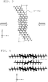
- Figure 3 is a schematic diagram schematically showing the view of the crystal structure of the organic semiconductor layer 30, as viewed from the b-axis direction
- Figure 4 is a schematic diagram schematically showing the view of the crystal structure of the organic semiconductor layer 30, as viewed from the a-axis direction
- Figure 5 is an explanatory diagram showing a relation between carrier mobility and magnitude of a strain in the organic semiconductor layer 30.
- the three crystal axes (the a-axis, the b-axis and the c-axis) are shown by arrows, and a unit cell is surrounded by a quadrangle.
- the carrier mobility changes depending on the magnitude of the given strain, as shown in Figure 5 .
- the carrier mobility is determined depending on the magnitude of the strain to be given, and increases as the strain to be given increases. For example, the carrier mobility when the strain is 3% is 16.5 [cm 2 /(V ⁇ s)], which is 1.7 times the carrier mobility when the strain is 0%.
- multi-crystal organic semiconductors differ in crystal structure, depending on the formation technique.
- FIG. 6 is a schematic diagram schematically showing how molecules vibrate before and after a compressive stress is applied to the single-crystal organic semiconductor.
- the single-crystal organic semiconductor has a property of increasing the carrier mobility as the strain to be given increases, and this property is consistent regardless of the formation technique for the organic semiconductor.
- the organic semiconductor layer 30 since the organic semiconductor layer 30 is formed as the single-crystal thin film, the organic semiconductor layer 30 can have uniform property with respect to the strain (the property of increasing the carrier mobility as the strain to be given increases).
- the magnitude of the strain of an object is detected, in the following procedure.
- a predetermined voltage is applied to the gauge leads 32 in a state where the substrate 22 sticks with the object to be detected.
- the strain of the object to be detected changes, the stress to be applied to the organic semiconductor layer 30 together with the substrate 22 changes, and the strain to be given to the organic semiconductor layer 30 changes.
- the strain to be given to the organic semiconductor layer 30 changes, the carrier mobility in the organic semiconductor layer 30 changes depending on the magnitude of the strain, and the gauge current to flow through the gauge leads 32 changes.
- the organic semiconductor element 20 by measuring the change in the gauge current, it is possible to measure the magnitude of the strain of the object to be detected.
- the organic semiconductor layer 30, which is formed as the single-crystal thin film has uniform property with respect to the strain, and therefore, it is possible to provide strain sensors having uniform property.
- the organic semiconductor layer 30 is formed as the single-crystal thin film, it is possible to measure the magnitude of the strain of the detection target. Further, since the organic semiconductor layer 30 is formed as the single-crystal thin film, it is possible to obtain the same carrier mobility when the same strain is given, and it is possible to provide strain sensors having uniform property.
- the organic semiconductor element 20 functions as a strain sensor.
- the organic semiconductor element 20 is not limited to elements that function as a strain sensor in this way, and may be used as any element that operates based on the carrier mobility when the strain changes (the carrier mobility when a predetermined strain as the standard is given and the carrier mobility when a different strain from the predetermined strain is given), as exemplified by a pressure sensor that detects the pressure given to a pressure sensitive part, and a temperature sensor that detects temperature.
- the organic semiconductor element may be stuck to a sheet, and based on the current (the carrier mobility) that flows when the strain of the organic semiconductor element changes by the press of the sheet, the pressure given to the sheet may be detected.
- the organic semiconductor element may be bonded to metals having different thermal expansion coefficients similarly to a bi-metal, and based on the current (the carrier mobility) when the strain of the organic semiconductor element changes due to the difference in thermal expansion coefficient caused by the change in temperature, the temperature may be detected.
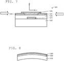
- FIG. 7 is an explanatory diagram showing an exemplary configuration of the organic semiconductor element 120 according to the second embodiment of the present invention.
- the organic semiconductor element 120 which is configured as a top contact-bottom gate type field-effect transistor, includes a substrate 122, a gate electrode 124 formed on a predetermined region of the substrate 122, a gate insulating film 126 formed on the substrate 122 and the gate electrode 124, an organic semiconductor layer 130 formed on the gate insulating film 126 so as to be positioned above the gate electrode 124, and a source electrode 132 and drain electrode 134 formed on the gate insulating film so as to be positioned on both sides of the organic semiconductor layer 130.
- the substrate 122 is formed of a plastic (for example, polyethylene naphthalate), such that the thickness is 50 ⁇ m to 10 mm, for example, 100 ⁇ m to 200 ⁇ m.
- a plastic for example, polyethylene naphthalate
- the gate electrode 124, the source electrode 132 and the drain electrode 134 are formed of a metal material such as gold.
- the gate electrode 124 is formed such that the thickness is 50 nm or less, for example, 40 nm or 30 nm.
- the source electrode 132 and the drain electrode 134 are formed such that the thickness is 50 nm or less, for example, 40 nm or 30 nm.
- the gate insulating film 126 is formed of an insulating material (for example, polymethyl methacrylate), such that the thickness is 200 nm or less, for example, 150 nm or 100 nm.
- an insulating material for example, polymethyl methacrylate
- the organic semiconductor layer 130 is formed such that the thickness is 200 nm or less, for example, 100 nm or 50 nm, as a single-crystal thin film of an organic semiconductor having the above-described structure shown in Formula (1).
- the organic semiconductor layer 130 is formed such that the c-axis of the crystal axes in the crystal structure shown in Figure 3 is parallel to the orientation of a channel to be formed, and is kept in a state where a predetermined strain is applied by applying a compressive stress in the c-axis direction.
- the "predetermined strain” only needs to be a strain by which the organic semiconductor layer 130, the substrate 122 or the gate insulating film 126 is not broken, and in the embodiment, a strain of 10% or less in the compression direction, for example, a strain of 3% in the compression direction can be used.
- FIG. 8 is an explanatory diagram showing an exemplary formation method for the organic semiconductor layer 130.
- a single-crystal thin film of the organic semiconductor (the organic semiconductor layer 30) is formed in the right-left direction in the figure, in a state where the substrate 122 having the gate insulating film 126 formed is bent. Thereafter, the substrate 122 is stretched until the substrate 122 becomes planar, and the compressive stress is applied to the thin film. Thereby, the organic semiconductor layer 130 kept in the state where the predetermined strain is applied is formed.
- the method for keeping the organic semiconductor layer 130 in a state where a predetermined strain is applied other than the method exemplified in Figure 8 , it is allowable to use another method such as a method of forming a single-crystal thin film of the organic semiconductor in a state where the substrate 122 is heated and is thermally expanded and thereafter thermally contracting the substrate 122 at normal temperature.
- the organic semiconductor layer 130 is formed as the single-crystal thin film in this way, it is possible to obtain the same carrier mobility when the same compressive stress is applied to and the same strain is given to the organic semiconductor layer 130. Accordingly, the organic semiconductor layer 130 can have uniform property with respect to the strain.
- the organic semiconductor element 120 configured in this way operates as a transistor, when a channel is formed in the organic semiconductor layer 130 by applying voltages for operation to the gate electrode 124, the source electrode 132 and the drain electrode 134 respectively.
- the organic semiconductor layer 130 which is formed as the single-crystal thin film, has uniform property with respect to the strain, and therefore, it is possible to provide transistors having uniform property. Further, since the organic semiconductor layer 130 is kept in the state where the strain is applied, the carrier mobility is higher compared to when the strain is not applied. Therefore, it is possible to make a larger current flow between the source electrode 132 and the drain electrode 134, and it is possible to provide a transistor having a higher drive power.
- the organic semiconductor layer 130 is formed as the single-crystal thin film, it is possible to provide a transistor having a high drive power. Further, since the organic semiconductor layer 130 is formed as the single-crystal thin film, it is possible to obtain the same carrier mobility when the same strain is given, and it is possible to provide transistors having uniform property.
- the organic semiconductor element 120 is configured as a top contact-bottom gate type field-effect transistor, but may be configured as any type of transistor that can be formed on an inorganic semiconductor such as silicon and gallium nitride, as exemplified by a top contact-top gate type field-effect transistor. Further, the organic semiconductor element is not limited to such transistor, and may be used as any element that can be kept in a state where a predetermined strain is applied in the movement direction of the carrier.
- the organic semiconductor layers 30, 130 are formed of the organic semiconductor having the above-described structure in Formula (1).
- the organic semiconductor for example, a polycyclic aromatic compound with four or more rings or a polycyclic compound with four or more rings including one or a plurality of unsaturated five-membered heterocyclic compounds and a plurality of benzene rings can be used.
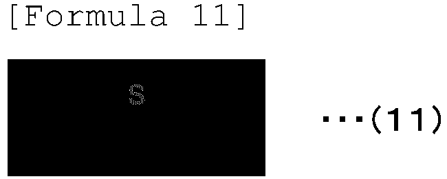
- any structure in the following Formula (2) to Formula (14) may be adopted.
- R a straight alkyl, a branched alkyl, a fluorinated straight/branched alkyl, triisopropylsilylethynyl, phenyl or the like can be used.
- the present invention can be utilized in production industries for an organic semiconductor element, and the like.
Landscapes
- Physics & Mathematics (AREA)
- Engineering & Computer Science (AREA)
- Chemical & Material Sciences (AREA)
- Materials Engineering (AREA)
- Spectroscopy & Molecular Physics (AREA)
- General Physics & Mathematics (AREA)
- Manufacturing & Machinery (AREA)
- Composite Materials (AREA)
- Thin Film Transistor (AREA)
- Electroluminescent Light Sources (AREA)
- Pressure Sensors (AREA)
Abstract
Description
- The present invention relates to an organic semiconductor element.
- Conventionally, as an organic semiconductor element of this type, there has been proposed an organic semiconductor element in which a compressive stress is applied to a multi-crystal or amorphous organic semiconductor (see Patent Literature 1, for example). In this device, the organic semiconductor is formed as a thin film on a bent substrate by a vapor deposition or a spin coating, and the compressive stress is applied to the organic semiconductor by stretching the bent substrate until the substrate becomes planar. With the compressive stress applied to the organic semiconductor, the carrier mobility of the organic semiconductor is increased.
- PTL 1:
JP2005-166742 - However, in the above-described organic semiconductor element, since a multi-crystal or amorphous organic semiconductor is used, it is difficult to obtain organic semiconductors having an identical multi-crystal structure or an identical amorphous structure. Because of the difference in the structure, even when organic semiconductors are produced by the same technique and the same compressive stress is applied so that the same strain is given, the organic semiconductors often differ in the carrier mobility, and it is difficult to obtain organic semiconductor elements having uniform property.
- A primary object of an organic semiconductor element in the present invention is to provide organic semiconductor elements having uniform property.
- For achieving the above-described primary object, an organic semiconductor element in the present invention adopts the following configurations.
- In the organic semiconductor element in the present invention, the organic semiconductor element includes an organic semiconductor. The organic semiconductor is formed as a single-crystal thin film, and the organic semiconductor element operates based on carrier mobility when a strain is given to at least the organic semiconductor.
- In the organic semiconductor element in the present invention, the organic semiconductor is formed as the single-crystal thin film. The crystal structure of a single crystal is determined by the molecules, and therefore, basically, an identical crystal structure is obtained regardless of the production technique. Therefore, when the same strain is given, the same carrier mobility can be obtained. Accordingly, it is possible to obtain organic semiconductor elements having uniform property.
- Here, the organic semiconductor may be formed as a thin film whose thickness is 200 nm or less, for example, 100 nm or 50 nm. It is preferable that the strain to be given to the organic semiconductor be in a range of 10% or less in a compression direction. Further, as the organic semiconductor, the organic semiconductor may be composed of a polycyclic aromatic compound with four or more rings, or a polycyclic compound with four or more rings including at least one unsaturated five-membered heterocyclic compound and a plurality of benzene rings.
- In the organic semiconductor element in the present invention, the organic semiconductor may be kept in a state where a predetermined strain is applied in a movement direction of carriers. That is, the organic semiconductor is used while the carrier mobility is fixed in the state where the predetermined strain is applied. By using such an organic semiconductor, it is possible to obtain various semiconductor devices.
- In the organic semiconductor element in the present invention, the organic semiconductor element may be operated based on mobility of carriers when a predetermined strain as a standard is given to the organic semiconductor and carrier mobility when a different strain from the predetermined strain is given to the organic semiconductor. Thereby, it is possible to use the organic semiconductor element as a sensor device.
-
- [
Figure 1] Figure 1 is an explanatory diagram showing an exemplary configuration of anorganic semiconductor element 20 according to a first embodiment of the present invention; - [
Figure 2] Figure 2 is an explanatory diagram showing an example of how anorganic semiconductor layer 30 is formed; - [
Figure 3] Figure 3 is a schematic diagram schematically showing the view of the crystal structure of theorganic semiconductor layer 30, as viewed from the b-axis direction; - [
Figure 4] Figure 4 is a schematic diagram schematically showing the view of the crystal structure of theorganic semiconductor layer 30, as viewed from the a-axis direction; - [
Figure 5] Figure 5 is an explanatory diagram showing a relation between mobility of carriers and magnitude of a strain in theorganic semiconductor layer 30; - [
Figure 6] Figure 6 is a schematic diagram schematically showing how molecules vibrate before and after a compressive stress is applied to a single-crystal organic semiconductor; - [
Figure 7] Figure 7 is an explanatory diagram showing an exemplary configuration of anorganic semiconductor element 120 according to a second embodiment of the present invention; and - [
Figure 8] Figure 8 is an explanatory diagram showing an exemplary formation method for anorganic semiconductor layer 130. - The following describes some aspects of the invention with reference to embodiment.
-
Figure 1 is an explanatory diagram showing an exemplary configuration of anorganic semiconductor element 20 that functions as a strain sensor according to a first embodiment of the present invention. Theorganic semiconductor element 20 includes asubstrate 22, anorganic semiconductor layer 30 formed on thesubstrate 22, and two gauge leads 32 formed on the organic semiconductor layer 30 (one of the twogauge leads 32 is not illustrated). - The
substrate 22 is formed of a plastic (for example, polyethylene naphthalate), such that the thickness is 50 µm to 10 mm, for example, 100 µm to 200 µm. - The
organic semiconductor layer 30 is formed such that the thickness is 200 nm or less, for example, 100 nm or 50 nm, as a single-crystal thin film of an organic semiconductor (for example, 3,11-didecyldinaphto [2,3-d:2',3'-d']benzo [1,2-b:4,5-b']dithiophene (C10-DNBDT) having a structure shown in the following Formula (1)).
- Here, a formation method for the
organic semiconductor layer 30 will be described.Figure 2 is an explanatory diagram showing an example of how theorganic semiconductor layer 30 is formed. First, ablade 50 is arranged above thesubstrate 22, so as to be nearly perpendicular to thesubstrate 22. At this time, theblade 50 is arranged such that the distance between thesubstrate 22 and atip 50a of theblade 50 is a predetermined distance (for example, 200 µm) that is greater than the thickness of theorganic semiconductor layer 30 to be formed. Then, while asolution 54 in which the organic semiconductor is dissolved in an aromatic compound (for example, o-dichlorobenzene) as a solvent is supplied to the gap between thesubstrate 22 and thetip 50a of theblade 50 from the left side inFigure 2 using asolution supply pipe 52, thesubstrate 22 is slowly moved in the right direction in the figure. Thereby, the solvent of thesolution 54 at a portion away from thetip 50a of theblade 50 evaporates, so that theorganic semiconductor layer 30 is formed as a single-crystal thin film. At this time, by matching the movement speed of thesubstrate 22 with the growth speed of the single crystal, it is possible to grow the single crystal from agrowth point 56 inFigure 2 , such that the single crystal has a uniform thickness. Here, in the embodiment, thesubstrate 22 is moved in the right direction in the figure, but theblade 50 and thesolution supply pipe 52 may be moved instead of the movement of thesubstrate 22. -
Figure 3 is a schematic diagram schematically showing the view of the crystal structure of theorganic semiconductor layer 30, as viewed from the b-axis direction,Figure 4 is a schematic diagram schematically showing the view of the crystal structure of theorganic semiconductor layer 30, as viewed from the a-axis direction, andFigure 5 is an explanatory diagram showing a relation between carrier mobility and magnitude of a strain in theorganic semiconductor layer 30. InFigures 3 and 4 , the three crystal axes (the a-axis, the b-axis and the c-axis) are shown by arrows, and a unit cell is surrounded by a quadrangle. In theorganic semiconductor layer 30, for example, when a compressive stress is applied in the direction (the direction shown by the broad arrows inFigure 3 ) parallel to the c-axis in the crystal structure of the organic semiconductor and a strain is given to theorganic semiconductor layer 30, the carrier mobility changes depending on the magnitude of the given strain, as shown inFigure 5 . The carrier mobility is determined depending on the magnitude of the strain to be given, and increases as the strain to be given increases. For example, the carrier mobility when the strain is 3% is 16.5 [cm2/(V·s)], which is 1.7 times the carrier mobility when the strain is 0%. Generally, multi-crystal organic semiconductors differ in crystal structure, depending on the formation technique. Therefore, even when the same compressive stress is applied and the same strain is given, it is not possible to obtain the same carrier mobility. In contrast, in single-crystal organic semiconductors, the crystal structure is determined by the molecule. Therefore, basically, an identical crystal structure is obtained regardless of the formation technique, and it is possible to obtain the same carrier mobility when the same compressive stress is applied and the same strain is given. Therefore, the single-crystal organic semiconductors have uniform property with respect to the strain. As the reason for the increase in the carrier mobility, the following reason is conceivable.Figure 6 is a schematic diagram schematically showing how molecules vibrate before and after a compressive stress is applied to the single-crystal organic semiconductor. When the compressive stress is applied to the single-crystal organic semiconductor, it is thought that a strain occurs to the crystal, molecules come closer to each other and the movement of the carrier in the organic semiconductor becomes easier so that the carrier mobility increases. Further, when molecules come closer to each other, the vibration of molecules becomes smaller. Therefore, it is thought that after the compressive stress is applied, as illustrated, the vibration of molecules becomes smaller, the movement of the carrier in the organic semiconductor becomes easier and the carrier mobility increases, compared to before the compressive stress is applied. Furthermore, the distance among molecules becomes closer as the strain to be given to the crystal increases, and therefore, the carrier mobility increases as the strain to be given to the crystal increases. Thus, the single-crystal organic semiconductor has a property of increasing the carrier mobility as the strain to be given increases, and this property is consistent regardless of the formation technique for the organic semiconductor. In the embodiment, since theorganic semiconductor layer 30 is formed as the single-crystal thin film, theorganic semiconductor layer 30 can have uniform property with respect to the strain (the property of increasing the carrier mobility as the strain to be given increases). - In the
organic semiconductor element 20 configured in this way, the magnitude of the strain of an object is detected, in the following procedure. First, a predetermined voltage is applied to the gauge leads 32 in a state where thesubstrate 22 sticks with the object to be detected. When the strain of the object to be detected changes, the stress to be applied to theorganic semiconductor layer 30 together with thesubstrate 22 changes, and the strain to be given to theorganic semiconductor layer 30 changes. When the strain to be given to theorganic semiconductor layer 30 changes, the carrier mobility in theorganic semiconductor layer 30 changes depending on the magnitude of the strain, and the gauge current to flow through the gauge leads 32 changes. In theorganic semiconductor element 20, by measuring the change in the gauge current, it is possible to measure the magnitude of the strain of the object to be detected. Further, theorganic semiconductor layer 30, which is formed as the single-crystal thin film, has uniform property with respect to the strain, and therefore, it is possible to provide strain sensors having uniform property. - According to the above-described
organic semiconductor element 20 in the first embodiment that functions as a strain sensor device, since theorganic semiconductor layer 30 is formed as the single-crystal thin film, it is possible to measure the magnitude of the strain of the detection target. Further, since theorganic semiconductor layer 30 is formed as the single-crystal thin film, it is possible to obtain the same carrier mobility when the same strain is given, and it is possible to provide strain sensors having uniform property. - In the first embodiment, the
organic semiconductor element 20 functions as a strain sensor. However, theorganic semiconductor element 20 is not limited to elements that function as a strain sensor in this way, and may be used as any element that operates based on the carrier mobility when the strain changes (the carrier mobility when a predetermined strain as the standard is given and the carrier mobility when a different strain from the predetermined strain is given), as exemplified by a pressure sensor that detects the pressure given to a pressure sensitive part, and a temperature sensor that detects temperature. For example, in the case of the use as a pressure sensor, the organic semiconductor element may be stuck to a sheet, and based on the current (the carrier mobility) that flows when the strain of the organic semiconductor element changes by the press of the sheet, the pressure given to the sheet may be detected. Further, in the case of the use as a temperature sensor, the organic semiconductor element may be bonded to metals having different thermal expansion coefficients similarly to a bi-metal, and based on the current (the carrier mobility) when the strain of the organic semiconductor element changes due to the difference in thermal expansion coefficient caused by the change in temperature, the temperature may be detected. - Next, an
organic semiconductor element 120 in a second embodiment that functions as a transistor will be described.Figure 7 is an explanatory diagram showing an exemplary configuration of theorganic semiconductor element 120 according to the second embodiment of the present invention. Theorganic semiconductor element 120, which is configured as a top contact-bottom gate type field-effect transistor, includes asubstrate 122, agate electrode 124 formed on a predetermined region of thesubstrate 122, agate insulating film 126 formed on thesubstrate 122 and thegate electrode 124, anorganic semiconductor layer 130 formed on thegate insulating film 126 so as to be positioned above thegate electrode 124, and asource electrode 132 anddrain electrode 134 formed on the gate insulating film so as to be positioned on both sides of theorganic semiconductor layer 130. - The
substrate 122 is formed of a plastic (for example, polyethylene naphthalate), such that the thickness is 50 µm to 10 mm, for example, 100 µm to 200 µm. - The
gate electrode 124, thesource electrode 132 and thedrain electrode 134 are formed of a metal material such as gold. Thegate electrode 124 is formed such that the thickness is 50 nm or less, for example, 40 nm or 30 nm. Thesource electrode 132 and thedrain electrode 134 are formed such that the thickness is 50 nm or less, for example, 40 nm or 30 nm. - The
gate insulating film 126 is formed of an insulating material (for example, polymethyl methacrylate), such that the thickness is 200 nm or less, for example, 150 nm or 100 nm. - The
organic semiconductor layer 130 is formed such that the thickness is 200 nm or less, for example, 100 nm or 50 nm, as a single-crystal thin film of an organic semiconductor having the above-described structure shown in Formula (1). Theorganic semiconductor layer 130 is formed such that the c-axis of the crystal axes in the crystal structure shown inFigure 3 is parallel to the orientation of a channel to be formed, and is kept in a state where a predetermined strain is applied by applying a compressive stress in the c-axis direction. Here, the "predetermined strain" only needs to be a strain by which theorganic semiconductor layer 130, thesubstrate 122 or thegate insulating film 126 is not broken, and in the embodiment, a strain of 10% or less in the compression direction, for example, a strain of 3% in the compression direction can be used. - Here, a formation method for the
organic semiconductor layer 130 will be described.Figure 8 is an explanatory diagram showing an exemplary formation method for theorganic semiconductor layer 130. First, as illustrated, a single-crystal thin film of the organic semiconductor (the organic semiconductor layer 30) is formed in the right-left direction in the figure, in a state where thesubstrate 122 having thegate insulating film 126 formed is bent. Thereafter, thesubstrate 122 is stretched until thesubstrate 122 becomes planar, and the compressive stress is applied to the thin film. Thereby, theorganic semiconductor layer 130 kept in the state where the predetermined strain is applied is formed. As the method for keeping theorganic semiconductor layer 130 in a state where a predetermined strain is applied, other than the method exemplified inFigure 8 , it is allowable to use another method such as a method of forming a single-crystal thin film of the organic semiconductor in a state where thesubstrate 122 is heated and is thermally expanded and thereafter thermally contracting thesubstrate 122 at normal temperature. - Since the
organic semiconductor layer 130 is formed as the single-crystal thin film in this way, it is possible to obtain the same carrier mobility when the same compressive stress is applied to and the same strain is given to theorganic semiconductor layer 130. Accordingly, theorganic semiconductor layer 130 can have uniform property with respect to the strain. - The
organic semiconductor element 120 configured in this way operates as a transistor, when a channel is formed in theorganic semiconductor layer 130 by applying voltages for operation to thegate electrode 124, thesource electrode 132 and thedrain electrode 134 respectively. Theorganic semiconductor layer 130, which is formed as the single-crystal thin film, has uniform property with respect to the strain, and therefore, it is possible to provide transistors having uniform property. Further, since theorganic semiconductor layer 130 is kept in the state where the strain is applied, the carrier mobility is higher compared to when the strain is not applied. Therefore, it is possible to make a larger current flow between thesource electrode 132 and thedrain electrode 134, and it is possible to provide a transistor having a higher drive power. - According to the above-described
organic semiconductor element 120 in the second embodiment that functions as a transistor, since theorganic semiconductor layer 130 is formed as the single-crystal thin film, it is possible to provide a transistor having a high drive power. Further, since theorganic semiconductor layer 130 is formed as the single-crystal thin film, it is possible to obtain the same carrier mobility when the same strain is given, and it is possible to provide transistors having uniform property. - In the second embodiment, the
organic semiconductor element 120 is configured as a top contact-bottom gate type field-effect transistor, but may be configured as any type of transistor that can be formed on an inorganic semiconductor such as silicon and gallium nitride, as exemplified by a top contact-top gate type field-effect transistor. Further, the organic semiconductor element is not limited to such transistor, and may be used as any element that can be kept in a state where a predetermined strain is applied in the movement direction of the carrier. - In the
organic semiconductor elements 




- There may be many other modifications, changes, and alterations without departing from the scope or spirit of the main characteristics of the present invention.
- The present invention can be utilized in production industries for an organic semiconductor element, and the like.
Claims (6)
- An organic semiconductor element comprises an organic semiconductor, wherein
the organic semiconductor is formed as a single-crystal thin film, and
the organic semiconductor element operates based on carrier mobility when a strain is given to at least the organic semiconductor. - The organic semiconductor element according to claim 1, wherein
the organic semiconductor is kept in a state where a predetermined strain is applied in a movement direction of carriers. - The organic semiconductor element according to claim 1, wherein
the organic semiconductor element operates based on carrier mobility when a predetermined strain as a standard is given to the organic semiconductor and carrier mobility when a different strain from the predetermined strain is given to the organic semiconductor. - The organic semiconductor element according to any one of claims 1 to 3, wherein
the organic semiconductor is composed of a polycyclic aromatic compound with four or more rings, or a polycyclic compound with four or more rings including at least one unsaturated five-membered heterocyclic compound and a plurality of benzene rings. - The organic semiconductor element according to any one of claims 1 to 4, wherein
the organic semiconductor is formed as a thin film having a thickness of 200 nm or less. - The organic semiconductor element according to any one of claims 1 to 5, wherein
the strain to be given to the organic semiconductor is in a range of 10% or less in a compression direction.
Applications Claiming Priority (2)
| Application Number | Priority Date | Filing Date | Title |
|---|---|---|---|
| JP2015015744A JP6116018B2 (en) | 2015-01-29 | 2015-01-29 | Organic semiconductor device |
| PCT/JP2016/052266 WO2016121791A1 (en) | 2015-01-29 | 2016-01-27 | Organic semiconductor element |
Publications (2)
| Publication Number | Publication Date |
|---|---|
| EP3252829A1 true EP3252829A1 (en) | 2017-12-06 |
| EP3252829A4 EP3252829A4 (en) | 2018-09-26 |
Family
ID=56543402
Family Applications (1)
| Application Number | Title | Priority Date | Filing Date |
|---|---|---|---|
| EP16743394.5A Pending EP3252829A4 (en) | 2015-01-29 | 2016-01-27 | Organic semiconductor element |
Country Status (5)
| Country | Link |
|---|---|
| US (2) | US10854825B2 (en) |
| EP (1) | EP3252829A4 (en) |
| JP (1) | JP6116018B2 (en) |
| CN (2) | CN107431095B (en) |
| WO (1) | WO2016121791A1 (en) |
Cited By (1)
| Publication number | Priority date | Publication date | Assignee | Title |
|---|---|---|---|---|
| CN112997332A (en) * | 2018-09-04 | 2021-06-18 | 国立大学法人东京大学 | Organic semiconductor element, strain sensor, vibration sensor, and method for manufacturing organic semiconductor element |
Families Citing this family (5)
| Publication number | Priority date | Publication date | Assignee | Title |
|---|---|---|---|---|
| US20220140265A1 (en) * | 2019-02-22 | 2022-05-05 | The University Of Tokyo | Organic semiconductor device, method for manufacturing organic semiconductor single crystal film, and method for manufacturing organic semiconductor device |
| CN110487455A (en) * | 2019-08-07 | 2019-11-22 | 北京理工大学 | A Light-Assisted Method for Improving the Sensitivity of Stress Sensors |
| JP7493228B2 (en) * | 2019-09-03 | 2024-05-31 | 国立研究開発法人産業技術総合研究所 | Organic semiconductor materials and organic thin film transistors |
| CN115210682A (en) * | 2020-03-19 | 2022-10-18 | 深圳纽迪瑞科技开发有限公司 | Pressure induction type structure and electronic product |
| JPWO2024043005A1 (en) | 2022-08-22 | 2024-02-29 |
Family Cites Families (21)
| Publication number | Priority date | Publication date | Assignee | Title |
|---|---|---|---|---|
| WO2004008545A1 (en) * | 2002-07-15 | 2004-01-22 | Pioneer Corporation | Organic semiconductor device and method for manufacturing same |
| JP2005079204A (en) * | 2003-08-28 | 2005-03-24 | Canon Inc | Field effect transistor and manufacturing method thereof |
| JP4736318B2 (en) | 2003-11-28 | 2011-07-27 | Tdk株式会社 | Manufacturing method of laminated body and manufacturing method of organic field effect transistor |
| US20050211973A1 (en) * | 2004-03-23 | 2005-09-29 | Kiyotaka Mori | Stressed organic semiconductor |
| US8030645B2 (en) | 2004-10-25 | 2011-10-04 | Panasonic Corporation | Electronic device, process for producing the same and electronic equipment making use thereof |
| US7671448B2 (en) * | 2005-03-24 | 2010-03-02 | Semiconductor Energy Laboratory Co., Ltd. | Semiconductor device including two organic semiconductor layers |
| US7977149B2 (en) * | 2005-08-31 | 2011-07-12 | Sumitomo Chemical Company, Limited | Transistor, organic semiconductor device, and method for manufacture of the transistor or device |
| CN101461047B (en) | 2006-06-07 | 2011-06-15 | 松下电器产业株式会社 | Semiconductor element, method for manufacturing the semiconductor element, electronic device and method for manufacturing the electronic device |
| CN101926017B (en) * | 2007-12-17 | 2013-09-25 | 3M创新有限公司 | Solution processable organic semiconductors based on anthracene |
| JP5478189B2 (en) | 2009-10-16 | 2014-04-23 | 学校法人東海大学 | Organic transistor with excellent atmospheric stability |
| WO2011074232A1 (en) * | 2009-12-14 | 2011-06-23 | 出光興産株式会社 | Polycyclic ring-fused compound and organic thin film transistor utilizing same |
| JP2011242153A (en) * | 2010-05-14 | 2011-12-01 | Citizen Holdings Co Ltd | Strain sensor and strain measuring method |
| WO2012165612A1 (en) * | 2011-06-03 | 2012-12-06 | 国立大学法人九州大学 | Organic semiconductor material, and organic electronics device |
| JP5950251B2 (en) * | 2011-09-09 | 2016-07-13 | 国立研究開発法人物質・材料研究機構 | Organic semiconductor single crystal formation method |
| JPWO2013065582A1 (en) * | 2011-11-04 | 2015-04-02 | ソニー株式会社 | Organic semiconductor device manufacturing method, organic semiconductor device, organic single crystal thin film growth method, organic single crystal thin film, electronic device, and organic single crystal thin film group |
| JP2013159584A (en) * | 2012-02-07 | 2013-08-19 | Univ Of Tokyo | Electronic material and electronic element using the same |
| JP2014049722A (en) * | 2012-09-04 | 2014-03-17 | Nec Corp | Organic semiconductor transistor and manufacturing method of the same |
| JP6008158B2 (en) * | 2013-03-05 | 2016-10-19 | Jnc株式会社 | Chalcogen-containing organic compounds and uses thereof |
| KR102196923B1 (en) * | 2013-04-25 | 2020-12-31 | 파이 크리스탈 가부시키가이샤 | Organic semiconductor thin film production method |
| WO2015137304A1 (en) | 2014-03-12 | 2015-09-17 | Dic株式会社 | Compound, organic semiconductor material containing same, organic semiconductor ink, and organic transistor |
| JP6590361B2 (en) | 2014-03-20 | 2019-10-16 | パイクリスタル株式会社 | Organic semiconductor film and manufacturing method thereof |
-
2015
- 2015-01-29 JP JP2015015744A patent/JP6116018B2/en active Active
-
2016
- 2016-01-27 WO PCT/JP2016/052266 patent/WO2016121791A1/en not_active Ceased
- 2016-01-27 CN CN201680018138.1A patent/CN107431095B/en active Active
- 2016-01-27 CN CN202110544249.9A patent/CN113285023A/en active Pending
- 2016-01-27 US US15/547,594 patent/US10854825B2/en active Active
- 2016-01-27 EP EP16743394.5A patent/EP3252829A4/en active Pending
-
2019
- 2019-07-03 US US16/502,174 patent/US10903434B2/en active Active
Cited By (3)
| Publication number | Priority date | Publication date | Assignee | Title |
|---|---|---|---|---|
| CN112997332A (en) * | 2018-09-04 | 2021-06-18 | 国立大学法人东京大学 | Organic semiconductor element, strain sensor, vibration sensor, and method for manufacturing organic semiconductor element |
| EP3848987A4 (en) * | 2018-09-04 | 2022-05-25 | The University of Tokyo | ORGANIC SEMICONDUCTOR ELEMENT, STRESS SENSOR, VIBRATION SENSOR AND METHOD FOR MAKING ORGANIC SEMICONDUCTOR ELEMENT |
| US12068093B2 (en) | 2018-09-04 | 2024-08-20 | The University Of Tokyo | Organic semiconductor element, strain sensor, vibration sensor, and manufacturing method for organic semiconductor element |
Also Published As
| Publication number | Publication date |
|---|---|
| US20180145266A1 (en) | 2018-05-24 |
| US10903434B2 (en) | 2021-01-26 |
| CN107431095B (en) | 2021-06-01 |
| US20190326522A1 (en) | 2019-10-24 |
| WO2016121791A1 (en) | 2016-08-04 |
| US10854825B2 (en) | 2020-12-01 |
| JP2016143675A (en) | 2016-08-08 |
| CN107431095A (en) | 2017-12-01 |
| JP6116018B2 (en) | 2017-04-19 |
| EP3252829A4 (en) | 2018-09-26 |
| CN113285023A (en) | 2021-08-20 |
Similar Documents
| Publication | Publication Date | Title |
|---|---|---|
| US10903434B2 (en) | Organic semiconductor element | |
| US10504756B2 (en) | Wafer processing method and apparatus | |
| Munzenrieder et al. | Design rules for IGZO logic gates on plastic foil enabling operation at bending radii of 3.5 mm | |
| Li et al. | Oxide semiconductor thin film transistors on thin solution-cast flexible substrates | |
| KR20140032093A (en) | Pressure sensor and pressure sensing method | |
| Richter et al. | Piezoresistance of silicon and strained Si0. 9Ge0. 1 | |
| Lee et al. | Mobility enhancement of strained Si transistors by transfer printing on plastic substrates | |
| Nguyen et al. | High-temperature tolerance of the piezoresistive effect in p-4H-SiC for harsh environment sensing | |
| Rojas et al. | Nonplanar nanoscale fin field effect transistors on textile, paper, wood, stone, and vinyl via soft material-enabled double-transfer printing | |
| GB2534675A8 (en) | Compound semiconductor device structures comprising polycrystalline CVD diamond | |
| CN102832177A (en) | Method for controlled removal of semiconductor device layer from base substrate | |
| US9666493B2 (en) | Semiconductor device structure with 110-PFET and 111-NFET curent flow direction | |
| Niu et al. | Epitaxial systems combining oxides and semiconductors | |
| US9972723B2 (en) | Piezoelectric thin-film based flexible sensing device, method for fabrication thereof and method for operating the same | |
| Ling et al. | Non-destructive probing of the anisotropy of field-effect mobility in the rubrene single crystal | |
| Phan et al. | Orientation dependence of the pseudo-Hall effect in p-type 3C–SiC four-terminal devices under mechanical stress | |
| KR101611811B1 (en) | Annealing a buffer layer for fabricating electronic devices on compliant substrates | |
| EP2653844A1 (en) | Integrated piezoelectric sensor for static pressure measurement | |
| JP6635466B2 (en) | Organic semiconductor device | |
| EP2690418A1 (en) | Pressure sensor having flexible diaphragm with active circuit components thereon | |
| WO2015038131A3 (en) | Variable ice and methods for measuring sample properties with the same | |
| US20090294853A1 (en) | Thin film transistor having a common channel and selectable doping configuration | |
| US10840377B2 (en) | Flexible high performance inorganic matter FET using built-in strain of inorganic matter on insulator wafer | |
| Seok et al. | A study on effect of wafer bow in wafer-level BCB cap transfer packaging | |
| Ghoneim et al. | Ultra-high density out-of-plane strain sensor 3D architecture based on sub-20 nm PMOS FinFET |
Legal Events
| Date | Code | Title | Description |
|---|---|---|---|
| STAA | Information on the status of an ep patent application or granted ep patent |
Free format text: STATUS: THE INTERNATIONAL PUBLICATION HAS BEEN MADE |
|
| PUAI | Public reference made under article 153(3) epc to a published international application that has entered the european phase |
Free format text: ORIGINAL CODE: 0009012 |
|
| STAA | Information on the status of an ep patent application or granted ep patent |
Free format text: STATUS: REQUEST FOR EXAMINATION WAS MADE |
|
| 17P | Request for examination filed |
Effective date: 20170828 |
|
| AK | Designated contracting states |
Kind code of ref document: A1 Designated state(s): AL AT BE BG CH CY CZ DE DK EE ES FI FR GB GR HR HU IE IS IT LI LT LU LV MC MK MT NL NO PL PT RO RS SE SI SK SM TR |
|
| AX | Request for extension of the european patent |
Extension state: BA ME |
|
| DAV | Request for validation of the european patent (deleted) | ||
| DAX | Request for extension of the european patent (deleted) | ||
| A4 | Supplementary search report drawn up and despatched |
Effective date: 20180823 |
|
| RIC1 | Information provided on ipc code assigned before grant |
Ipc: H01L 21/336 20060101ALI20180817BHEP Ipc: H01L 29/84 20060101ALI20180817BHEP Ipc: H01L 29/786 20060101AFI20180817BHEP Ipc: H01L 51/05 20060101ALI20180817BHEP Ipc: G01L 1/18 20060101ALI20180817BHEP |
|
| STAA | Information on the status of an ep patent application or granted ep patent |
Free format text: STATUS: EXAMINATION IS IN PROGRESS |
|
| 17Q | First examination report despatched |
Effective date: 20200709 |
|
| RIC1 | Information provided on ipc code assigned before grant |
Ipc: H01L 21/336 19900101ALI20230112BHEP Ipc: H01L 29/786 19950101AFI20230112BHEP |
|
| GRAP | Despatch of communication of intention to grant a patent |
Free format text: ORIGINAL CODE: EPIDOSNIGR1 |
|
| STAA | Information on the status of an ep patent application or granted ep patent |
Free format text: STATUS: GRANT OF PATENT IS INTENDED |
|
| INTG | Intention to grant announced |
Effective date: 20240528 |
|
| GRAJ | Information related to disapproval of communication of intention to grant by the applicant or resumption of examination proceedings by the epo deleted |
Free format text: ORIGINAL CODE: EPIDOSDIGR1 |
|
| STAA | Information on the status of an ep patent application or granted ep patent |
Free format text: STATUS: EXAMINATION IS IN PROGRESS |
|
| INTC | Intention to grant announced (deleted) | ||
| REG | Reference to a national code |
Ref country code: DE Ref legal event code: R079 Free format text: PREVIOUS MAIN CLASS: H01L0029786000 Ipc: H10K0077000000 |
|
| GRAP | Despatch of communication of intention to grant a patent |
Free format text: ORIGINAL CODE: EPIDOSNIGR1 |
|
| STAA | Information on the status of an ep patent application or granted ep patent |
Free format text: STATUS: GRANT OF PATENT IS INTENDED |
|
| RIC1 | Information provided on ipc code assigned before grant |
Ipc: H10K 77/00 20230101AFI20260326BHEP |