EP3252827A1 - Semiconductor device and manufacturing method therefor - Google Patents
Semiconductor device and manufacturing method therefor Download PDFInfo
- Publication number
- EP3252827A1 EP3252827A1 EP17173729.9A EP17173729A EP3252827A1 EP 3252827 A1 EP3252827 A1 EP 3252827A1 EP 17173729 A EP17173729 A EP 17173729A EP 3252827 A1 EP3252827 A1 EP 3252827A1
- Authority
- EP
- European Patent Office
- Prior art keywords
- pseudo gate
- gate structure
- fin
- insulator layer
- pseudo
- Prior art date
- Legal status (The legal status is an assumption and is not a legal conclusion. Google has not performed a legal analysis and makes no representation as to the accuracy of the status listed.)
- Withdrawn
Links
Images





Classifications
-
- H—ELECTRICITY
- H10—SEMICONDUCTOR DEVICES; ELECTRIC SOLID-STATE DEVICES NOT OTHERWISE PROVIDED FOR
- H10D—INORGANIC ELECTRIC SEMICONDUCTOR DEVICES
- H10D30/00—Field-effect transistors [FET]
- H10D30/01—Manufacture or treatment
- H10D30/021—Manufacture or treatment of FETs having insulated gates [IGFET]
- H10D30/024—Manufacture or treatment of FETs having insulated gates [IGFET] of fin field-effect transistors [FinFET]
-
- H—ELECTRICITY
- H10—SEMICONDUCTOR DEVICES; ELECTRIC SOLID-STATE DEVICES NOT OTHERWISE PROVIDED FOR
- H10D—INORGANIC ELECTRIC SEMICONDUCTOR DEVICES
- H10D30/00—Field-effect transistors [FET]
- H10D30/60—Insulated-gate field-effect transistors [IGFET]
- H10D30/62—Fin field-effect transistors [FinFET]
-
- H—ELECTRICITY
- H10—SEMICONDUCTOR DEVICES; ELECTRIC SOLID-STATE DEVICES NOT OTHERWISE PROVIDED FOR
- H10D—INORGANIC ELECTRIC SEMICONDUCTOR DEVICES
- H10D30/00—Field-effect transistors [FET]
- H10D30/60—Insulated-gate field-effect transistors [IGFET]
- H10D30/791—Arrangements for exerting mechanical stress on the crystal lattice of the channel regions
- H10D30/797—Arrangements for exerting mechanical stress on the crystal lattice of the channel regions being in source or drain regions, e.g. SiGe source or drain
-
- H—ELECTRICITY
- H10—SEMICONDUCTOR DEVICES; ELECTRIC SOLID-STATE DEVICES NOT OTHERWISE PROVIDED FOR
- H10D—INORGANIC ELECTRIC SEMICONDUCTOR DEVICES
- H10D62/00—Semiconductor bodies, or regions thereof, of devices having potential barriers
- H10D62/01—Manufacture or treatment
- H10D62/021—Forming source or drain recesses by etching e.g. recessing by etching and then refilling
-
- H—ELECTRICITY
- H10—SEMICONDUCTOR DEVICES; ELECTRIC SOLID-STATE DEVICES NOT OTHERWISE PROVIDED FOR
- H10D—INORGANIC ELECTRIC SEMICONDUCTOR DEVICES
- H10D62/00—Semiconductor bodies, or regions thereof, of devices having potential barriers
- H10D62/10—Shapes, relative sizes or dispositions of the regions of the semiconductor bodies; Shapes of the semiconductor bodies
- H10D62/113—Isolations within a component, i.e. internal isolations
- H10D62/115—Dielectric isolations, e.g. air gaps
-
- H—ELECTRICITY
- H10—SEMICONDUCTOR DEVICES; ELECTRIC SOLID-STATE DEVICES NOT OTHERWISE PROVIDED FOR
- H10D—INORGANIC ELECTRIC SEMICONDUCTOR DEVICES
- H10D62/00—Semiconductor bodies, or regions thereof, of devices having potential barriers
- H10D62/80—Semiconductor bodies, or regions thereof, of devices having potential barriers characterised by the materials
- H10D62/82—Heterojunctions
- H10D62/822—Heterojunctions comprising only Group IV materials heterojunctions, e.g. Si/Ge heterojunctions
-
- H—ELECTRICITY
- H10—SEMICONDUCTOR DEVICES; ELECTRIC SOLID-STATE DEVICES NOT OTHERWISE PROVIDED FOR
- H10D—INORGANIC ELECTRIC SEMICONDUCTOR DEVICES
- H10D62/00—Semiconductor bodies, or regions thereof, of devices having potential barriers
- H10D62/80—Semiconductor bodies, or regions thereof, of devices having potential barriers characterised by the materials
- H10D62/83—Semiconductor bodies, or regions thereof, of devices having potential barriers characterised by the materials being Group IV materials, e.g. B-doped Si or undoped Ge
- H10D62/832—Semiconductor bodies, or regions thereof, of devices having potential barriers characterised by the materials being Group IV materials, e.g. B-doped Si or undoped Ge being Group IV materials comprising two or more elements, e.g. SiGe
-
- H—ELECTRICITY
- H10—SEMICONDUCTOR DEVICES; ELECTRIC SOLID-STATE DEVICES NOT OTHERWISE PROVIDED FOR
- H10D—INORGANIC ELECTRIC SEMICONDUCTOR DEVICES
- H10D62/00—Semiconductor bodies, or regions thereof, of devices having potential barriers
- H10D62/80—Semiconductor bodies, or regions thereof, of devices having potential barriers characterised by the materials
- H10D62/83—Semiconductor bodies, or regions thereof, of devices having potential barriers characterised by the materials being Group IV materials, e.g. B-doped Si or undoped Ge
- H10D62/832—Semiconductor bodies, or regions thereof, of devices having potential barriers characterised by the materials being Group IV materials, e.g. B-doped Si or undoped Ge being Group IV materials comprising two or more elements, e.g. SiGe
- H10D62/8325—Silicon carbide
-
- H—ELECTRICITY
- H10—SEMICONDUCTOR DEVICES; ELECTRIC SOLID-STATE DEVICES NOT OTHERWISE PROVIDED FOR
- H10D—INORGANIC ELECTRIC SEMICONDUCTOR DEVICES
- H10D84/00—Integrated devices formed in or on semiconductor substrates that comprise only semiconducting layers, e.g. on Si wafers or on GaAs-on-Si wafers
- H10D84/01—Manufacture or treatment
- H10D84/0123—Integrating together multiple components covered by H10D12/00 or H10D30/00, e.g. integrating multiple IGBTs
- H10D84/0126—Integrating together multiple components covered by H10D12/00 or H10D30/00, e.g. integrating multiple IGBTs the components including insulated gates, e.g. IGFETs
- H10D84/0165—Integrating together multiple components covered by H10D12/00 or H10D30/00, e.g. integrating multiple IGBTs the components including insulated gates, e.g. IGFETs the components including complementary IGFETs, e.g. CMOS devices
- H10D84/017—Manufacturing their source or drain regions, e.g. silicided source or drain regions
-
- H—ELECTRICITY
- H10—SEMICONDUCTOR DEVICES; ELECTRIC SOLID-STATE DEVICES NOT OTHERWISE PROVIDED FOR
- H10D—INORGANIC ELECTRIC SEMICONDUCTOR DEVICES
- H10D84/00—Integrated devices formed in or on semiconductor substrates that comprise only semiconducting layers, e.g. on Si wafers or on GaAs-on-Si wafers
- H10D84/01—Manufacture or treatment
- H10D84/0123—Integrating together multiple components covered by H10D12/00 or H10D30/00, e.g. integrating multiple IGBTs
- H10D84/0126—Integrating together multiple components covered by H10D12/00 or H10D30/00, e.g. integrating multiple IGBTs the components including insulated gates, e.g. IGFETs
- H10D84/0165—Integrating together multiple components covered by H10D12/00 or H10D30/00, e.g. integrating multiple IGBTs the components including insulated gates, e.g. IGFETs the components including complementary IGFETs, e.g. CMOS devices
- H10D84/0172—Manufacturing their gate conductors
-
- H—ELECTRICITY
- H10—SEMICONDUCTOR DEVICES; ELECTRIC SOLID-STATE DEVICES NOT OTHERWISE PROVIDED FOR
- H10D—INORGANIC ELECTRIC SEMICONDUCTOR DEVICES
- H10D84/00—Integrated devices formed in or on semiconductor substrates that comprise only semiconducting layers, e.g. on Si wafers or on GaAs-on-Si wafers
- H10D84/01—Manufacture or treatment
- H10D84/0123—Integrating together multiple components covered by H10D12/00 or H10D30/00, e.g. integrating multiple IGBTs
- H10D84/0126—Integrating together multiple components covered by H10D12/00 or H10D30/00, e.g. integrating multiple IGBTs the components including insulated gates, e.g. IGFETs
- H10D84/0165—Integrating together multiple components covered by H10D12/00 or H10D30/00, e.g. integrating multiple IGBTs the components including insulated gates, e.g. IGFETs the components including complementary IGFETs, e.g. CMOS devices
- H10D84/0188—Manufacturing their isolation regions
-
- H—ELECTRICITY
- H10—SEMICONDUCTOR DEVICES; ELECTRIC SOLID-STATE DEVICES NOT OTHERWISE PROVIDED FOR
- H10D—INORGANIC ELECTRIC SEMICONDUCTOR DEVICES
- H10D84/00—Integrated devices formed in or on semiconductor substrates that comprise only semiconducting layers, e.g. on Si wafers or on GaAs-on-Si wafers
- H10D84/01—Manufacture or treatment
- H10D84/0123—Integrating together multiple components covered by H10D12/00 or H10D30/00, e.g. integrating multiple IGBTs
- H10D84/0126—Integrating together multiple components covered by H10D12/00 or H10D30/00, e.g. integrating multiple IGBTs the components including insulated gates, e.g. IGFETs
- H10D84/0165—Integrating together multiple components covered by H10D12/00 or H10D30/00, e.g. integrating multiple IGBTs the components including insulated gates, e.g. IGFETs the components including complementary IGFETs, e.g. CMOS devices
- H10D84/0193—Integrating together multiple components covered by H10D12/00 or H10D30/00, e.g. integrating multiple IGBTs the components including insulated gates, e.g. IGFETs the components including complementary IGFETs, e.g. CMOS devices the components including FinFETs
-
- H—ELECTRICITY
- H10—SEMICONDUCTOR DEVICES; ELECTRIC SOLID-STATE DEVICES NOT OTHERWISE PROVIDED FOR
- H10D—INORGANIC ELECTRIC SEMICONDUCTOR DEVICES
- H10D84/00—Integrated devices formed in or on semiconductor substrates that comprise only semiconducting layers, e.g. on Si wafers or on GaAs-on-Si wafers
- H10D84/01—Manufacture or treatment
- H10D84/02—Manufacture or treatment characterised by using material-based technologies
- H10D84/03—Manufacture or treatment characterised by using material-based technologies using Group IV technology, e.g. silicon technology or silicon-carbide [SiC] technology
- H10D84/038—Manufacture or treatment characterised by using material-based technologies using Group IV technology, e.g. silicon technology or silicon-carbide [SiC] technology using silicon technology, e.g. SiGe
-
- H—ELECTRICITY
- H10—SEMICONDUCTOR DEVICES; ELECTRIC SOLID-STATE DEVICES NOT OTHERWISE PROVIDED FOR
- H10D—INORGANIC ELECTRIC SEMICONDUCTOR DEVICES
- H10D84/00—Integrated devices formed in or on semiconductor substrates that comprise only semiconducting layers, e.g. on Si wafers or on GaAs-on-Si wafers
- H10D84/80—Integrated devices formed in or on semiconductor substrates that comprise only semiconducting layers, e.g. on Si wafers or on GaAs-on-Si wafers characterised by the integration of at least one component covered by groups H10D12/00 or H10D30/00, e.g. integration of IGFETs
- H10D84/82—Integrated devices formed in or on semiconductor substrates that comprise only semiconducting layers, e.g. on Si wafers or on GaAs-on-Si wafers characterised by the integration of at least one component covered by groups H10D12/00 or H10D30/00, e.g. integration of IGFETs of only field-effect components
- H10D84/83—Integrated devices formed in or on semiconductor substrates that comprise only semiconducting layers, e.g. on Si wafers or on GaAs-on-Si wafers characterised by the integration of at least one component covered by groups H10D12/00 or H10D30/00, e.g. integration of IGFETs of only field-effect components of only insulated-gate FETs [IGFET]
- H10D84/85—Complementary IGFETs, e.g. CMOS
- H10D84/853—Complementary IGFETs, e.g. CMOS comprising FinFETs
-
- H—ELECTRICITY
- H10—SEMICONDUCTOR DEVICES; ELECTRIC SOLID-STATE DEVICES NOT OTHERWISE PROVIDED FOR
- H10D—INORGANIC ELECTRIC SEMICONDUCTOR DEVICES
- H10D84/00—Integrated devices formed in or on semiconductor substrates that comprise only semiconducting layers, e.g. on Si wafers or on GaAs-on-Si wafers
- H10D84/80—Integrated devices formed in or on semiconductor substrates that comprise only semiconducting layers, e.g. on Si wafers or on GaAs-on-Si wafers characterised by the integration of at least one component covered by groups H10D12/00 or H10D30/00, e.g. integration of IGFETs
- H10D84/82—Integrated devices formed in or on semiconductor substrates that comprise only semiconducting layers, e.g. on Si wafers or on GaAs-on-Si wafers characterised by the integration of at least one component covered by groups H10D12/00 or H10D30/00, e.g. integration of IGFETs of only field-effect components
- H10D84/83—Integrated devices formed in or on semiconductor substrates that comprise only semiconducting layers, e.g. on Si wafers or on GaAs-on-Si wafers characterised by the integration of at least one component covered by groups H10D12/00 or H10D30/00, e.g. integration of IGFETs of only field-effect components of only insulated-gate FETs [IGFET]
- H10D84/85—Complementary IGFETs, e.g. CMOS
- H10D84/856—Complementary IGFETs, e.g. CMOS the complementary IGFETs having different architectures than each other, e.g. high-voltage and low-voltage CMOS
-
- H—ELECTRICITY
- H10—SEMICONDUCTOR DEVICES; ELECTRIC SOLID-STATE DEVICES NOT OTHERWISE PROVIDED FOR
- H10P—GENERIC PROCESSES OR APPARATUS FOR THE MANUFACTURE OR TREATMENT OF DEVICES COVERED BY CLASS H10
- H10P50/00—Etching of wafers, substrates or parts of devices
- H10P50/20—Dry etching; Plasma etching; Reactive-ion etching
- H10P50/28—Dry etching; Plasma etching; Reactive-ion etching of insulating materials
- H10P50/282—Dry etching; Plasma etching; Reactive-ion etching of insulating materials of inorganic materials
- H10P50/283—Dry etching; Plasma etching; Reactive-ion etching of insulating materials of inorganic materials by chemical means
-
- H—ELECTRICITY
- H10—SEMICONDUCTOR DEVICES; ELECTRIC SOLID-STATE DEVICES NOT OTHERWISE PROVIDED FOR
- H10P—GENERIC PROCESSES OR APPARATUS FOR THE MANUFACTURE OR TREATMENT OF DEVICES COVERED BY CLASS H10
- H10P50/00—Etching of wafers, substrates or parts of devices
- H10P50/73—Etching of wafers, substrates or parts of devices using masks for insulating materials
-
- H—ELECTRICITY
- H10—SEMICONDUCTOR DEVICES; ELECTRIC SOLID-STATE DEVICES NOT OTHERWISE PROVIDED FOR
- H10P—GENERIC PROCESSES OR APPARATUS FOR THE MANUFACTURE OR TREATMENT OF DEVICES COVERED BY CLASS H10
- H10P76/00—Manufacture or treatment of masks on semiconductor bodies, e.g. by lithography or photolithography
- H10P76/40—Manufacture or treatment of masks on semiconductor bodies, e.g. by lithography or photolithography of masks comprising inorganic materials
- H10P76/405—Manufacture or treatment of masks on semiconductor bodies, e.g. by lithography or photolithography of masks comprising inorganic materials characterised by their composition, e.g. multilayer masks
-
- H—ELECTRICITY
- H10—SEMICONDUCTOR DEVICES; ELECTRIC SOLID-STATE DEVICES NOT OTHERWISE PROVIDED FOR
- H10P—GENERIC PROCESSES OR APPARATUS FOR THE MANUFACTURE OR TREATMENT OF DEVICES COVERED BY CLASS H10
- H10P76/00—Manufacture or treatment of masks on semiconductor bodies, e.g. by lithography or photolithography
- H10P76/40—Manufacture or treatment of masks on semiconductor bodies, e.g. by lithography or photolithography of masks comprising inorganic materials
- H10P76/408—Manufacture or treatment of masks on semiconductor bodies, e.g. by lithography or photolithography of masks comprising inorganic materials characterised by their sizes, orientations, dispositions, behaviours or shapes
- H10P76/4085—Manufacture or treatment of masks on semiconductor bodies, e.g. by lithography or photolithography of masks comprising inorganic materials characterised by their sizes, orientations, dispositions, behaviours or shapes characterised by the processes involved to create the masks
-
- H—ELECTRICITY
- H10—SEMICONDUCTOR DEVICES; ELECTRIC SOLID-STATE DEVICES NOT OTHERWISE PROVIDED FOR
- H10D—INORGANIC ELECTRIC SEMICONDUCTOR DEVICES
- H10D64/00—Electrodes of devices having potential barriers
- H10D64/01—Manufacture or treatment
- H10D64/013—Manufacture or treatment of electrodes having a conductor capacitively coupled to a semiconductor by an insulator
- H10D64/01302—Manufacture or treatment of electrodes having a conductor capacitively coupled to a semiconductor by an insulator the insulator being formed after the semiconductor body, the semiconductor being silicon
- H10D64/01304—Manufacture or treatment of electrodes having a conductor capacitively coupled to a semiconductor by an insulator the insulator being formed after the semiconductor body, the semiconductor being silicon characterised by the conductor
- H10D64/01306—Manufacture or treatment of electrodes having a conductor capacitively coupled to a semiconductor by an insulator the insulator being formed after the semiconductor body, the semiconductor being silicon characterised by the conductor the conductor comprising a layer of silicon contacting the insulator, e.g. polysilicon
-
- H—ELECTRICITY
- H10—SEMICONDUCTOR DEVICES; ELECTRIC SOLID-STATE DEVICES NOT OTHERWISE PROVIDED FOR
- H10D—INORGANIC ELECTRIC SEMICONDUCTOR DEVICES
- H10D64/00—Electrodes of devices having potential barriers
- H10D64/60—Electrodes characterised by their materials
- H10D64/66—Electrodes having a conductor capacitively coupled to a semiconductor by an insulator, e.g. MIS electrodes
- H10D64/661—Electrodes having a conductor capacitively coupled to a semiconductor by an insulator, e.g. MIS electrodes the conductor comprising a layer of silicon contacting the insulator, e.g. polysilicon having vertical doping variation
Definitions
- the present invention relates to the technical field of semiconductors, and in particular, to a semiconductor device and a manufacturing method therefor.
- a Fin Field Effect Transistor (FinFET) device is capable of improving performance of a device, reducing a supply voltage, and significantly reducing short-channel effects.
- some problems may occur during an existing method for manufacturing a FinFET device.
- a source and a drain are needed in an N metal oxide semiconductor (NMOS) transistor and a P metal oxide semiconductor (PMOS) transistor.
- NMOS N metal oxide semiconductor
- PMOS P metal oxide semiconductor
- a source and a drain formed on a fin through an epitaxial process may be irregular, which influences performance and uniformity of a device.
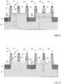
- FIG. 1A and FIG. 1B There are two designs in the prior art, respectively referred to in FIG. 1A and FIG. 1B . However, there may be some problems for the two designs, separately.
- three pseudo gates are formed on each of two fins that are isolated by a trench.
- three pseudo gates 11, 12, and 13 are formed on the left fin. If drifting of a pseudo gate relative to an active region occurs in a manufacturing process of a device (for example, in FIG. 1A , the three pseudo gates on the left fin drift leftwards relative to the active region below and the three pseudo gate on the right fin drift rightwards relative to the active region below, or a key dimension of a pseudo gate may also change), a result of an undesired source or drain formed at peripheries of the fins may be probably caused.
- a source (or drain) 14 on the left fin and a drain (or source) 15 on the right fin, as shown in FIG. 1A may be caused
- the source (or drain) 14 may be connected to the drain (or source) 15, thereby reducing performance of the device.
- pseudo gates 22 and 23 are formed on a left fin and a right fin, respectively, and a pseudo gate 21 is formed on an insulator 26 for filling a trench between the two fins.
- a source or a drain the epitaxial growth of a source and a drain at peripheries of the fins in contact with the insulator 26 may be constrained, so as to cause an irregular appearance of source (or drain) 24 on the left fin or a drain (or source) 25 on the right fin, as shown in FIG. 1B , thereby influencing performance of the device.
- an object of the present invention to provide manufacturing method for a semiconductor device and a semiconductor device, in which at least one of the above discussed problems is solved or at least reduced, in particular an intentionally connecting of a source (or drain) on a fin to a source (or drain) on another fin can be avoided.
- a first aspect of the present invention provides a manufacturing method for a semiconductor device.
- a second aspect of the present invention provides a semiconductor device.
- the present invention can prevent a source (or drain) on a fin from being undesirably connected to a source (or drain) on another fin.
- the first aspect of the present invention provides a manufacturing method for a semiconductor device, including: providing a substrate structure, where the substrate structure includes: a semiconductor substrate; a fin protruding from the semiconductor substrate, where trenches are formed on the sides of the fin; a first insulator layer partially filling the trenches, where the fin protrudes from the first insulator layer; and a second insulator layer covering the fin.
- the method further includes forming a plurality of pseudo gate structures on the second insulator layer, where each pseudo gate structure wraps a part of the fin, where the pseudo gate structure includes a pseudo gate located on the second insulator layer, and the plurality of pseudo gate structures includes at least a first pseudo gate structure and a second pseudo gate structure that are spaced from each other; and the second pseudo gate structure is located at an edge corner of the fin, and a part of the second pseudo gate structure is on the first insulator layer.
- the method further includes forming, on the first insulator layer and the second insulator layer, spacers at two sides of each of the plurality of pseudo gate structures; etching the second insulator layer and at least a part of the fin that are not covered by the spacers and the pseudo gates, to form a recess in the fin; and forming a source or a drain in the recess.
- the plurality of pseudo gate structures further includes a third pseudo gate structure spaced from the first pseudo gate structure, where the second pseudo gate structure and the third pseudo gate structure are located at two sides of the first pseudo gate structure, respectively; and the third pseudo gate structure is located at an edge corner of the fin, and a part of the third pseudo gate structure is on the first insulator layer.
- the step of forming a recess includes: forming, in the fin, a first recess located between the first pseudo gate structure and the second pseudo gate structure and a second recess located between the first pseudo gate structure and the third pseudo gate structure through the etching.
- the step of forming a source or a drain in the recess includes: forming a source in the first recess and forming a drain in the second recess.
- the material of the pseudo gate includes polysilicon.
- the pseudo gate structure further includes a hard mask layer located on the pseudo gate.
- the material of the hard mask layer includes silicon nitride.
- the second pseudo gate structure is spaced from the first pseudo gate structure for a first distance, where the first distance ranges from 60 nm to 100 nm.
- the third pseudo gate structure is spaced from the first pseudo gate structure for a second distance, where the second distance ranges from 60 nm to 100 nm.
- the manufacturing method further includes: forming an interlayer dielectric layer to cover the substrate structure after the source or the drain is formed; etching back the interlayer dielectric layer, to expose an upper surface of the hard mask layer; removing the hard mask layer, the pseudo gate, and a part of the second insulator layer, so as to form an opening; and forming a gate structure in the opening.
- the gate structure includes: a gate insulator layer that is on the fin and wraps a part of the fin, and a gate on the gate insulator layer.
- the fin is an N-well region, and the material of the source or the drain includes silicon germanium; or the fin is a P-well region, and the material of the source or the drain includes silicon carbide.
- the substrate structure includes multiple fins, including a first fin for forming a PMOS device and a second fin for forming an NMOS device, where the material of the source or the drain on the first fin includes silicon germanium; and the material of the source or the drain on the second fin includes silicon carbide.
- the second aspect of the present invention provides a semiconductor device, including: a semiconductor substrate; a fin protruding from the semiconductor substrate, where trenches are formed on the sides of the fin; a first insulator layer partially filling the trenches, where the fin protrudes from the first insulator layer; a second insulator layer covering the fin; a plurality of pseudo gate structures on the second insulator layer, where each pseudo gate structure wraps a part of the fin, where the pseudo gate structure includes a pseudo gate located on the second insulator layer, and the plurality of pseudo gate structures includes at least a first pseudo gate structure and a second pseudo gate structure that are spaced from each other; and the second pseudo gate structure is located at an edge corner of the fin, and a part of the second pseudo gate structure is on the first insulator layer; spacers, on the first insulator layer and the second insulator layer, at two sides of each of the plurality of pseudo gate structures; and a source or a drain on the fin and located among the plurality of pseudo gate
- the plurality of pseudo gate structures further includes a third pseudo gate structure spaced from the first pseudo gate structure, where the second pseudo gate structure and the third pseudo gate structure are located at two sides of the first pseudo gate structure, respectively; and the third pseudo gate structure is located at an edge corner of the fin, and a part of the third pseudo gate structure is on the first insulator layer.
- the material of the pseudo gate includes polysilicon.
- the material of the hard mask layer includes silicon nitride.
- the second pseudo gate structure is spaced from the first pseudo gate structure for a first distance, where the first distance ranges from 60 nm to 100 nm.
- the source includes a source between the first pseudo gate structure and the second pseudo gate structure; and the drain includes a drain located between the first pseudo gate structure and the third pseudo gate structure.
- the fin is an N-well region, and the material of the source or the drain includes silicon germanium; or the fin is a P-well region, and the material of the source or the drain includes silicon carbide.
- the semiconductor device includes multiple fins, including a first fin for forming a PMOS device and a second fin for forming an NMOS device, where the material of the source or the drain on the first fin includes silicon germanium; and the material of the source or the drain on the second fin includes silicon carbide.
- the present invention can prevent a source (or drain) on a fin from being undesirably connected to a source (or drain) on another fin, thereby being capable of improving reliability of the device.
- the present invention can also enable a formed source and drain to have a regular appearance, thereby being capable of improving performance of the device.
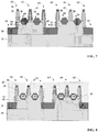
- FIG. 3 schematically illustrates a structural schematic diagram of a cross section of step S201.
- a substrate structure 30 is provided.
- the substrate structure 30 may include a semiconductor substrate 31.
- the semiconductor substrate may be, for example, a silicon substrate.
- the substrate structure 30 may further include one or multiple fins (for example, a first fin 41 and a second fin 42 shown in FIG. 3 ) protruding from the semiconductor substrate 31. Trenches 43 are formed on sides of each fin.
- the fin is a semiconductor fin.
- the material of the fin may include silicon.
- the substrate structure 30 may further include a first insulator layer 32 partially filling the trenches 43. The fin protrudes from the first insulator layer 32.
- the material of the first insulator layer may include silicon dioxide, for example.
- the substrate structure 30 may further include a second insulator layer 33 covering the fins.
- the material of the second insulator layer may include silicon dioxide, for example.
- FIG. 3 shows two fins, a person skilled in the art should understand that fins with a quantity larger than or less than two may be formed on the semiconductor substrate 31, and therefore the present invention is not limited thereto.
- step S202 a plurality of pseudo gate structures that is on the second insulator layer is formed, where each pseudo gate structure wraps a part of a fin.
- FIG. 4 schematically illustrates a structural schematic diagram of a cross section of step S202.
- a plurality of pseudo gate structures is formed on the second insulator layer 33, and each pseudo gate structure wraps a part of a fin.
- the pseudo gate structure may include a pseudo gate 35 located on the second insulator layer 33.
- the material of the pseudo gate may include polysilicon, for example.
- the pseudo gate structure may further include a hard mask layer 36 located on the pseudo gate 35.
- the material of the hard mask layer may include silicon nitride, for example.
- the plurality of pseudo gate structures includes at least a first pseudo gate structure and a second pseudo gate structure that are spaced from each other.
- the plurality of pseudo gate structures includes at least a first pseudo gate structure 51 and a second pseudo gate structure 52 that are spaced from each other.
- the plurality of pseudo gate structures includes at least a first pseudo gate structure 61 and a second pseudo gate structure 62 that are spaced from each other.
- the second pseudo gate structure is located at an edge corner of a fin and a part of the second pseudo gate structure is located on the first insulator layer.
- the second pseudo gate structure 52 is located at an edge corner of a fin (for example, the first fin 41) and a part of the second pseudo gate structure 52 is located on the first insulator layer 32.
- the plurality of pseudo gate structures may further include a third pseudo gate structure spaced from the first pseudo gate structure.
- the plurality of pseudo gate structures may further include a third pseudo gate structure 53 spaced from the first pseudo gate structure 51.
- the plurality of pseudo gate structures may further include a third pseudo gate structure 63 spaced from the first pseudo gate structure 61.
- the second pseudo gate structure 52 and the third pseudo gate structure 53 are located at two sides of the first pseudo gate structure 51, respectively, the third pseudo gate structure 53 is located at an edge corner of a fin (for example, the first fin 41), and a part of the third pseudo gate structure 53 is located on the first insulator layer 32.
- first pseudo gate structure 51, the second pseudo gate structure 52, and the third pseudo gate structure 53 on the first fin 41 are used as main objects to be described in the present invention.
- descriptions of the second pseudo gate structure 52, and the third pseudo gate structure 53 on the first fin 41 may also be equally or similarly applicable to descriptions of the first pseudo gate structure 61, the second pseudo gate structure 62, and the third pseudo gate structure 63 on the second fin 42.
- the third pseudo gate structure (for example, the third pseudo gate structure 53) is spaced from the first pseudo gate structure (for example, the first pseudo gate structure 51) for a second distance.
- the second distance may range from 60 nm to 100 nm, for example, 70 nm, 80 nm, or 90 nm.
- the step of forming the plurality of pseudo gate structures may include: for example, as shown in FIG. 12 , forming a pseudo gate material layer 35 on the substrate structure through a deposition process for example, forming a hard mask layer 36 on the pseudo gate material layer 35 through a deposition process for example, and forming a first patterned mask layer (for example, a photoresist) 44 on the hard mask layer 36 through a coating process for example.
- the first mask layer 44 is used as an etching barrier layer to etch the hard mask layer 36 and the pseudo gate material layer 35, and then the first mask layer 44 is removed to form the structure shown in FIG. 4 .
- step S203 spacers are formed at two sides of each of the plurality of pseudo gate structures on the first insulator layer and the second insulator layer.
- FIG. 5 schematically illustrates a structural schematic diagram of a cross section of step S203.
- spacers 37 are formed on the first insulator layer 32 and the second insulator layer 33 at two sides of each of the plurality of pseudo gate structures.
- the spacers 37 are formed at two sides of the first pseudo gate structure 51, the second pseudo gate structure 52, and the third pseudo gate structure 53 on the first fin 41.
- the spacers 37 are formed at two sides of the first pseudo gate structure 61, the second pseudo gate structure 62, and the third pseudo gate structure 63 on the second fin 42.
- the material of the spacers may include, for example, a silicon oxide or a silicon nitride.
- step S204 at least one part of the second insulator layer and the fin that are not covered by the spacers and the pseudo gates are etched to form a recess.
- FIG. 6 schematically illustrates a structural schematic diagram of a cross section of step S204.
- the second insulator layer 33 and the fin for example, the first fin 41 or the second fin 42
- the spacers 37 and the pseudo gates 35 is etched by using the spacers and the pseudo gates or the hard mask layer formed on the pseudo gates as an etching barrier layer through an anisotropic etching process for example, so as to form a recess (for example, a recess 38 or 39) in the fin.
- the step of forming a recess may include that: a first recess located between the first pseudo gate structure and the second pseudo gate structure and a second recess between the first pseudo gate structure and the third pseudo gate structure may be formed in the fin through the etching.
- a first recess 38 between the first pseudo gate structure 51 and the second pseudo gate structure 52 and a second recess 39 between the first pseudo gate structure 51 and the third pseudo gate structure 53 may be formed in the first fin 41 through the etching.
- FIG. 6 a first recess 38 between the first pseudo gate structure 51 and the second pseudo gate structure 52 and a second recess 39 between the first pseudo gate structure 51 and the third pseudo gate structure 53 may be formed in the first fin 41 through the etching.
- a first recess 38 between the first pseudo gate structure 61 and the second pseudo gate structure 62 and a second recess 39 between the first pseudo gate structure 61 and the third pseudo gate structure 63 may be formed in the second fin 42 through the etching.
- step S205 a source or a drain is formed in the recess.
- the step may include: forming a source in the first recess and forming a drain in the second recess.
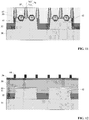
- FIG. 7 schematically illustrates a structural schematic diagram of a cross section of step S205.
- a source 45 is formed in the first recess 38 of the first fin 41 and a drain 46 is formed in the second recess 39 of the first fin 41 through an epitaxial growth process for example.
- a source 55 is formed in the first recess 38 of the second fin 42 and a drain 56 is formed in the second recess 39 of the second fin 42 through an epitaxial growth process for example.
- the fin may be an N-well region.
- the material of the source or the drain may include silicon germanium (SiGe).
- the one or multiple fins may all be an N-well region.
- one or some fins of the one or multiple fins are N-well regions.
- the respective material of the source and the drain formed on the fin of the N-well regions may include SiGe.
- the fin may be a P-well region.
- the material of the source or the drain may include silicon carbide (SiC).
- the one or multiple fins may all be a P-well region.
- one or some fins of the one or multiple fins are P-well regions.
- the respective material of the source and the drain formed on the fin of the P-well regions may include SiC.
- the one or multiple fins may include a first fin (for example, the first fin 41) for forming a PMOS device and a second fin (for example, the second fin 42) for forming the NMOS device.
- the material of the source (for example, the source 45) or the drain (for example, the drain 46) on the first fin (for example, the first fin 41) may include silicon germanium.
- the material of the source (for example, the source 55) or the drain (for example, the drain 56) on the second fin (for example, the second fin 42) may include silicon carbide.
- a manufacturing method for a semiconductor device is provided.
- Forms of the manufacturing method of the present invention can prevent a source (or drain) on one fin from being undesirably connected to a source (or drain) on another fin, thereby being capable of improving reliability of the device.
- Forms of the manufacturing method of the present invention can also enable a formed source and drain to have a regular appearance, thereby being capable of improving performance of the device.
- the manufacturing method may further include that: as shown in FIG. 8 , an interlayer dielectric layer 47 may be formed through a deposition process for example, so as to cover the substrate structure after the source or the drain is formed.
- the material of the interlayer dielectric layer may include silicon dioxide.
- the manufacturing method may further include: as shown in FIG. 9 , the interlayer dielectric layer 47 is etched back, so as to expose an upper surface of the hard mask layer 36.
- the etching back may be implemented by using a planarization (for example chemical and mechanical planarization) process.
- the manufacturing method may further include: as shown in FIG. 11 , forming a gate structure 71 in the opening 57.
- the gate structure 71 may include: a gate insulator layer 711 on the fin (for example, the first fin 41 or the second fin 42) and wrapping a part of the fin, and a gate 712 on the gate insulator layer 711.
- the material of the gate insulator layer may include silicon dioxide or a k (dielectric constant) dielectric material.
- the material of the gate may include metals such as tungsten or aluminum.
- the step of forming a gate structure may include: for example, forming a gate insulator layer 711 on a bottom part or a sidewall of the opening 57 through a deposition process and then depositing a gate material, so as to fill the opening 57.
- planarization is performed on the gate material to form a gate 712.
- FIG. 13A to FIG. 13I schematically illustrate structural schematic diagrams of cross sections in several phases of a manufacturing process for a substrate structure.
- the manufacturing process for a substrate structure is described below with reference to FIG. 13A to FIG. 13I .
- a third insulator layer 81 is formed, as a buffering layer, on a semiconductor substrate (for example, a silicon substrate) 31 through a deposition or oxidation process for example.
- the material of the third insulator layer may include silicon dioxide, for example.
- a fourth insulator layer 82 is formed on the third insulator layer 81 through a deposition process for example.
- the material of the fourth insulator layer may include silicon nitride, for example.
- the structure shown in FIG. 13B is etched so as to form fins isolated by a trench, that is, semiconductor fins.
- a second patterned mask layer (not shown in FIG. 13C ) may be coated on the structure shown in FIG. 13B , then the fourth insulator layer 82, the third insulator layer 81, and the semiconductor substrate 31 are etched by using the second mask layer, so as to form fins, and then the second mask layer is removed.
- a fifth insulator layer 83 is formed on a surface of the structure shown in FIG. 13C through a deposition process for example.
- the material of the fifth insulator layer may include silicon dioxide, for example.
- a first insulator layer 32 is formed on the structure shown in FIG. 13D through a deposition process (for example, Flowable Chemical Vapor Deposition (FCVD)), so as to fill the trenches between the respective fins for example.
- a deposition process for example, Flowable Chemical Vapor Deposition (FCVD)
- the first insulator layer 32 and the fifth insulator layer 83 are planarized, so as to expose an upper surface of the fourth insulator layer 82.
- the first insulator layer 32 and the fifth insulator layer 83 are etched back, to enable the semiconductor fins to protrude from the first insulator layer 32.
- the fourth insulator layer 82 and the third insulator layer 81 are removed.
- a second insulator layer 33 is formed on a part of a surface of the fins through an oxidation process for example.
- the second insulator layer 33 may also be formed through a deposition process.
- the schematic diagram of the substrate structure shown in FIG. 3 may be regarded as a structural schematic diagram of a cross section taken from FIG. 13I along A-A'.
- the fifth insulator layer 83 in FIG. 13I is omitted in FIG. 3 .
- the substrate structure may further include a fifth insulator layer 83 located between the first insulator layer 32 and the semiconductor substrate 31 and between the first insulator layer 32 and the fin (for example, the first fin 41 or the second fin 42).
- the substrate structure also may not include the fifth insulator layer.
- the present invention further provides a semiconductor device.
- the semiconductor device may include a semiconductor substrate 31.
- the semiconductor substrate may be, for example, a silicon substrate.
- the semiconductor device may further include one or multiple fins protruding from the semiconductor substrate, for example, the first fin 41 and the second fin 42 shown in FIG. 7 .
- Trench 43 are formed at sides of each fin.
- the fin is a semiconductor fin.
- the material of the fin may include silicon.
- the semiconductor device may further include a first insulator layer 32 partially filling the trenches 43.
- the fin (for example, the first fin 41 or the second fin 42) protrudes from the first insulator layer 32.
- the material of the first insulator layer may include silicon dioxide, for example.
- the semiconductor device may further include a second insulator layer 33 covering the fin.
- the material of the second insulator layer may include silicon dioxide, for example.
- the semiconductor device may further include a plurality of pseudo gate structures that is on the second insulator layer 33, each of which wraps a part of the fin.
- the pseudo gate structure may include a pseudo gate 35 located on the second insulator layer 33.
- the material of the pseudo gate may include polysilicon, for example.
- the pseudo gate structure may further include a hard mask layer 36 located on the pseudo gate 35.
- the material of the hard mask layer may include silicon nitride, for example.
- the plurality of pseudo gate structures includes at least a first pseudo gate structure and a second pseudo gate structure that are spaced from each other.
- the plurality of pseudo gate structures includes at least a first pseudo gate structure 51 and a second pseudo gate structure 52 that are spaced from each other.
- the plurality of pseudo gate structures includes at least a first pseudo gate structure 61 and a second pseudo gate structure 62 that are spaced from each other.
- the second pseudo gate structure is located at an edge corner of a fin and a part of the second pseudo gate structure is located on the first insulator layer.
- the second pseudo gate structure 52 is located at an edge corner of the first fin 41 and a part of the second pseudo gate structure 52 is located on the first insulator layer 32.
- the plurality of pseudo gate structures may further include a third pseudo gate structure spaced from the first pseudo gate structure.
- the plurality of pseudo gate structures may further include a third pseudo gate structure 53 spaced from the first pseudo gate structure 51.
- the plurality of pseudo gate structures may further include a third pseudo gate structure 63 spaced from the first pseudo gate structure 61.
- the second pseudo gate structure 52 and the third pseudo gate structure 53 are located at two sides of the first pseudo gate structure 51, respectively, the third pseudo gate structure 53 is located at an edge corner of a fin (for example, the first fin 41), and a part of the third pseudo gate structure 53 is located on the first insulator layer 32.
- the second pseudo gate structure (for example, the second pseudo gate structure 52) is spaced from the first pseudo gate structure (for example, the first pseudo gate structure 51) for a first distance.
- the first distance may range from 60 nm to 100 nm, for example, 70 nm, 80 nm, or 90 nm.
- the third pseudo gate structure (for example, the third pseudo gate structure 53) is spaced from the first pseudo gate structure (for example, the first pseudo gate structure 51) for a second distance.
- the second distance may range from 60 nm to 100 nm, for example, 70 nm, 80 nm, or 90 nm.
- the semiconductor device may further include a first insulator layer 32 and a second insulator layer 33, and spacers 37 respectively at two sides of the plurality of pseudo gate structures.
- the semiconductor device may further include spacers 37 at two sides of the respective first pseudo gate structure 51, the second pseudo gate structure 52, and the third pseudo gate structure 53 on the first fin 41.
- the semiconductor device may further include spacers 37 at two sides of the respective first pseudo gate structure 61, the second pseudo gate structure 62, and the third pseudo gate structure 63 on the second fin 42.
- the material of the spacers may include, for example, a silicon oxide or a silicon nitride.
- the semiconductor device may further include a source or a drain located among the plurality of pseudo gate structures located on the fin.
- the source may include a source between the first pseudo gate structure and the second pseudo gate structure.
- the source may include the source 45 located between the first pseudo gate structure 51 and the second pseudo gate structure 52.
- the source may include the source 55 located between the first pseudo gate structure 61 and the second pseudo gate structure 62.
- the drain may include a drain between the first pseudo gate structure and the third pseudo gate structure.
- the drain may include the drain 46 located between the first pseudo gate structure 51 and the third pseudo gate structure 53.
- the drain may include the drain 56 located between the first pseudo gate structure 61 and the third pseudo gate structure 63.
- the fin may be an N-well region.
- the material of the source or the drain may include silicon germanium (SiGe).
- the one or multiple fins may be an N-well region.
- one or some fins of the one or multiple fins are N-well regions.
- the respective material of the source and the drain formed on the fin of the N-well regions may include SiGe.
- the fin may be a P-well region.
- the material of the source or the drain may include silicon carbide (SiC).
- the one or multiple fins may all be a P-well region.
- one or some fins of the one or multiple fins are P-well regions.
- the respective material of the source and the drain on the fin of the P-well regions may include SiC.
- the one or multiple fins may include a first fin (for example, the first fin 41) for forming a PMOS device and a second fin (for example, the second fin 42) for forming the NMOS device.
- the material of the source (for example, the source 45) or the drain (for example, the drain 46) on the first fin (for example, the first fin 41) may include silicon germanium.
- the material of the source (for example, the source 55) or the drain (for example, the drain 56) on the second fin (for example, the second fin 42) may include silicon carbide.
- Forms of the semiconductor device of the present invention can prevent a source (or drain) on one fin from being undesirably connected to a source (or drain) on another fin, thereby being capable of improving reliability of the device.
- Forms of the semiconductor device of the present invention can also enable a formed source and drain to have a regular appearance, thereby being capable of improving performance of the device.
Landscapes
- Insulated Gate Type Field-Effect Transistor (AREA)
- Metal-Oxide And Bipolar Metal-Oxide Semiconductor Integrated Circuits (AREA)
- Thin Film Transistor (AREA)
- Chemical & Material Sciences (AREA)
- Chemical Kinetics & Catalysis (AREA)
- General Chemical & Material Sciences (AREA)
Abstract
Description
- This application is based on and claims priority to Chinese patent Application
CN201610379168.7, filed June 1, 2016 - The present invention relates to the technical field of semiconductors, and in particular, to a semiconductor device and a manufacturing method therefor.
- A Fin Field Effect Transistor (FinFET) device is capable of improving performance of a device, reducing a supply voltage, and significantly reducing short-channel effects. However, some problems may occur during an existing method for manufacturing a FinFET device. For example, a source and a drain are needed in an N metal oxide semiconductor (NMOS) transistor and a P metal oxide semiconductor (PMOS) transistor. However, a source and a drain formed on a fin through an epitaxial process may be irregular, which influences performance and uniformity of a device.
- There are two designs in the prior art, respectively referred to in
FIG. 1A and FIG. 1B . However, there may be some problems for the two designs, separately. - For the design shown in
FIG. 1A , three pseudo gates are formed on each of two fins that are isolated by a trench. For example, threepseudo gates FIG. 1A , the three pseudo gates on the left fin drift leftwards relative to the active region below and the three pseudo gate on the right fin drift rightwards relative to the active region below, or a key dimension of a pseudo gate may also change), a result of an undesired source or drain formed at peripheries of the fins may be probably caused. For example, a source (or drain) 14 on the left fin and a drain (or source) 15 on the right fin, as shown inFIG. 1A , may be caused In an epitaxial process, the source (or drain) 14 may be connected to the drain (or source) 15, thereby reducing performance of the device. - For the design shown in
FIG. 1 B ,pseudo gates pseudo gate 21 is formed on aninsulator 26 for filling a trench between the two fins. During epitaxial growth of a source or a drain, the epitaxial growth of a source and a drain at peripheries of the fins in contact with theinsulator 26 may be constrained, so as to cause an irregular appearance of source (or drain) 24 on the left fin or a drain (or source) 25 on the right fin, as shown inFIG. 1B , thereby influencing performance of the device. - The problems in the prior art have been found by the inventors of the present invention and the inventors provide a novel technical solution with respect to at least one of the above discussed problems.
- It is, therefore, an object of the present invention to provide manufacturing method for a semiconductor device and a semiconductor device, in which at least one of the above discussed problems is solved or at least reduced, in particular an intentionally connecting of a source (or drain) on a fin to a source (or drain) on another fin can be avoided.
- The object is achieved by the features of the respective independent claims. Further embodiments are defined in the respective dependent claims.
- A first aspect of the present invention provides a manufacturing method for a semiconductor device. A second aspect of the present invention provides a semiconductor device. Amongst others, the present invention can prevent a source (or drain) on a fin from being undesirably connected to a source (or drain) on another fin.
- The first aspect of the present invention provides a manufacturing method for a semiconductor device, including: providing a substrate structure, where the substrate structure includes: a semiconductor substrate; a fin protruding from the semiconductor substrate, where trenches are formed on the sides of the fin; a first insulator layer partially filling the trenches, where the fin protrudes from the first insulator layer; and a second insulator layer covering the fin.
- Preferably, the method further includes forming a plurality of pseudo gate structures on the second insulator layer, where each pseudo gate structure wraps a part of the fin, where the pseudo gate structure includes a pseudo gate located on the second insulator layer, and the plurality of pseudo gate structures includes at least a first pseudo gate structure and a second pseudo gate structure that are spaced from each other; and the second pseudo gate structure is located at an edge corner of the fin, and a part of the second pseudo gate structure is on the first insulator layer.
- Preferably, the method further includes forming, on the first insulator layer and the second insulator layer, spacers at two sides of each of the plurality of pseudo gate structures; etching the second insulator layer and at least a part of the fin that are not covered by the spacers and the pseudo gates, to form a recess in the fin; and forming a source or a drain in the recess.
- Preferably, the plurality of pseudo gate structures further includes a third pseudo gate structure spaced from the first pseudo gate structure, where the second pseudo gate structure and the third pseudo gate structure are located at two sides of the first pseudo gate structure, respectively; and the third pseudo gate structure is located at an edge corner of the fin, and a part of the third pseudo gate structure is on the first insulator layer.
- Preferably, the step of forming a recess includes: forming, in the fin, a first recess located between the first pseudo gate structure and the second pseudo gate structure and a second recess located between the first pseudo gate structure and the third pseudo gate structure through the etching.
- Preferably, the step of forming a source or a drain in the recess includes: forming a source in the first recess and forming a drain in the second recess.
- Preferably, the material of the pseudo gate includes polysilicon.
- Preferably, the pseudo gate structure further includes a hard mask layer located on the pseudo gate.
- Preferably, the material of the hard mask layer includes silicon nitride.
- Preferably, the second pseudo gate structure is spaced from the first pseudo gate structure for a first distance, where the first distance ranges from 60 nm to 100 nm.
- Preferably, the third pseudo gate structure is spaced from the first pseudo gate structure for a second distance, where the second distance ranges from 60 nm to 100 nm.
- Preferably, the manufacturing method further includes: forming an interlayer dielectric layer to cover the substrate structure after the source or the drain is formed; etching back the interlayer dielectric layer, to expose an upper surface of the hard mask layer; removing the hard mask layer, the pseudo gate, and a part of the second insulator layer, so as to form an opening; and forming a gate structure in the opening.
- Preferably, the gate structure includes: a gate insulator layer that is on the fin and wraps a part of the fin, and a gate on the gate insulator layer.
- Preferably, the fin is an N-well region, and the material of the source or the drain includes silicon germanium; or the fin is a P-well region, and the material of the source or the drain includes silicon carbide.
- Preferably, the substrate structure includes multiple fins, including a first fin for forming a PMOS device and a second fin for forming an NMOS device, where the material of the source or the drain on the first fin includes silicon germanium; and the material of the source or the drain on the second fin includes silicon carbide.
- The second aspect of the present invention provides a semiconductor device, including: a semiconductor substrate; a fin protruding from the semiconductor substrate, where trenches are formed on the sides of the fin; a first insulator layer partially filling the trenches, where the fin protrudes from the first insulator layer; a second insulator layer covering the fin; a plurality of pseudo gate structures on the second insulator layer, where each pseudo gate structure wraps a part of the fin, where the pseudo gate structure includes a pseudo gate located on the second insulator layer, and the plurality of pseudo gate structures includes at least a first pseudo gate structure and a second pseudo gate structure that are spaced from each other; and the second pseudo gate structure is located at an edge corner of the fin, and a part of the second pseudo gate structure is on the first insulator layer; spacers, on the first insulator layer and the second insulator layer, at two sides of each of the plurality of pseudo gate structures; and a source or a drain on the fin and located among the plurality of pseudo gate structures.
- Preferably, the plurality of pseudo gate structures further includes a third pseudo gate structure spaced from the first pseudo gate structure, where the second pseudo gate structure and the third pseudo gate structure are located at two sides of the first pseudo gate structure, respectively; and the third pseudo gate structure is located at an edge corner of the fin, and a part of the third pseudo gate structure is on the first insulator layer.
- Preferably, the material of the pseudo gate includes polysilicon.
- Preferably, the pseudo gate structure further includes a hard mask layer located on the pseudo gate.
- Preferably, the material of the hard mask layer includes silicon nitride.
- Preferably, the second pseudo gate structure is spaced from the first pseudo gate structure for a first distance, where the first distance ranges from 60 nm to 100 nm.
- Preferably, the third pseudo gate structure is spaced from the first pseudo gate structure for a second distance, where the second distance ranges from 60 nm to 100 nm.
- Preferably, the source includes a source between the first pseudo gate structure and the second pseudo gate structure; and the drain includes a drain located between the first pseudo gate structure and the third pseudo gate structure.
- Preferably, the fin is an N-well region, and the material of the source or the drain includes silicon germanium; or the fin is a P-well region, and the material of the source or the drain includes silicon carbide.
- Preferably, the semiconductor device includes multiple fins, including a first fin for forming a PMOS device and a second fin for forming an NMOS device, where the material of the source or the drain on the first fin includes silicon germanium; and the material of the source or the drain on the second fin includes silicon carbide.
- The present invention can prevent a source (or drain) on a fin from being undesirably connected to a source (or drain) on another fin, thereby being capable of improving reliability of the device.
- The present invention can also enable a formed source and drain to have a regular appearance, thereby being capable of improving performance of the device.
- Other features and advantages of the present invention become clear by describing exemplary forms of the present invention in detail with reference to the accompanying drawings below.
- The accompanying drawings that constitute a part of the specification describe forms of the present invention, and together with the specification, are used to interpret the present invention.
- The present invention can be understood more clearly according to the detailed description below with reference to the accompanying drawings, where:
-
FIG. 1A schematically illustrates a structural schematic diagram of a cross section of a semiconductor device according to an embodiment of the prior art; -
FIG. 1B schematically illustrates a structural schematic diagram of a cross section of a semiconductor device according to another embodiment of the prior art; -
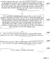
FIG. 2 is a flow chart of a manufacturing method for a semiconductor device; -
FIG. 3 schematically illustrates a structural schematic diagram of a cross section in a phase of the manufacturing process for a semiconductor device; -
FIG. 4 schematically illustrates a structural schematic diagram of a cross section in a phase of the manufacturing process for a semiconductor device; -
FIG. 5 schematically illustrates a structural schematic diagram of a cross section in a phase of the manufacturing process for a semiconductor device; -
FIG. 6 schematically illustrates a structural schematic diagram of a cross section in a phase of the manufacturing process for a semiconductor device; -
FIG. 7 schematically illustrates a structural schematic diagram of a cross section in a phase of the manufacturing process for a semiconductor device; -
FIG. 8 schematically illustrates a structural schematic diagram of a cross section in a phase of the manufacturing process for a semiconductor device; -
FIG. 9 schematically illustrates a structural schematic diagram of a cross section in a phase of the manufacturing process for a semiconductor device; -
FIG. 10 schematically illustrates a structural schematic diagram of a cross section in a phase of the manufacturing process for a semiconductor device; -
FIG. 11 schematically illustrates a structural schematic diagram of a cross section in a phase of the manufacturing process for a semiconductor device; -
FIG. 12 schematically illustrates a structural schematic diagram of a cross section in a phase of the manufacturing process for a semiconductor device; -
FIG. 13A schematically illustrates a structural schematic diagram of a cross section in a phase of the manufacturing process for a substrate structure; -
FIG. 13B schematically illustrates a structural schematic diagram of a cross section in a phase of the manufacturing process for a substrate structure; -
FIG. 13C schematically illustrates a structural schematic diagram of a cross section in a phase of the manufacturing process for a substrate structure; -
FIG. 13D schematically illustrates a structural schematic diagram of a cross section in a phase of the manufacturing process for a substrate structure; -
FIG. 13E schematically illustrates a structural schematic diagram of a cross section in a phase of the manufacturing process for a substrate structure; -
FIG. 13F schematically illustrates a structural schematic diagram of a cross section in a phase of the manufacturing process for a substrate structure; -
FIG. 13G schematically illustrates a structural schematic diagram of a cross section in a phase of the manufacturing process for a substrate structure; -
FIG. 13H schematically illustrates a structural schematic diagram of a cross section in a phase of the manufacturing process for a substrate structure; and -
FIG. 13I schematically illustrates a structural schematic diagram of a cross section in a phase of the manufacturing process for a substrate structure. - The present invention is described in detail with reference to the accompanying drawings and various exemplary forms. It should be noted that: unless otherwise specified, the relative arrangements of the components and steps, numeral expressions, and values stated in these forms are not intended to limit the present invention.
- Meanwhile, it should be understood that the sizes of the respective sections shown in the accompanying drawings are not drawn according to an actual proportion, so as to facilitate the description.
- The description of at least one exemplary form below is illustrative only and should not be taken as any limitation to the present invention and application or use thereof.
- The technology, methods, and devices that are known by a person of ordinary skill in the art are not discussed in detail, and in a proper situation, the technology, methods, and devices should be regarded as parts of the specification.
- Any specific values in all the examples shown and discussed herein should be understood as examples only, instead of limitations. Therefore, the other examples of the exemplary forms may have different values.
- It should be noted that: similar reference labels and letters in the following accompanying drawings indicate similar items. Therefore, once a certain item is defined in one accompanying drawing, the item needs not to be further discussed in the subsequent accompanying drawings.
-
FIG. 2 is a flow chart of a manufacturing method for a semiconductor device.FIG. 3 to FIG. 12 schematically illustrate structural schematic diagrams of cross sections in several phases of the manufacturing process for a semiconductor device. Some forms of a manufacturing process of a semiconductor device are described in detail below with reference toFIG. 2 andFIG. 3 toFIG. 12 . - As shown in
FIG. 2 , in step S201, a substrate structure is provided. -
FIG. 3 schematically illustrates a structural schematic diagram of a cross section of step S201. As shown inFIG. 3 , asubstrate structure 30 is provided. Thesubstrate structure 30 may include asemiconductor substrate 31. The semiconductor substrate may be, for example, a silicon substrate. Thesubstrate structure 30 may further include one or multiple fins (for example, afirst fin 41 and asecond fin 42 shown inFIG. 3 ) protruding from thesemiconductor substrate 31.Trenches 43 are formed on sides of each fin. The fin is a semiconductor fin. For example, the material of the fin may include silicon. Thesubstrate structure 30 may further include afirst insulator layer 32 partially filling thetrenches 43. The fin protrudes from thefirst insulator layer 32. The material of the first insulator layer may include silicon dioxide, for example. Thesubstrate structure 30 may further include asecond insulator layer 33 covering the fins. The material of the second insulator layer may include silicon dioxide, for example. - It should be noted that: although
FIG. 3 shows two fins, a person skilled in the art should understand that fins with a quantity larger than or less than two may be formed on thesemiconductor substrate 31, and therefore the present invention is not limited thereto. - In some forms, the fin may be an N-well region or a P-well region. For example, the
first fin 41 and thesecond fin 42 may both be N-well regions or may both be P-well regions, or one of thefirst fin 41 and thesecond fin 42 is an N-well region and the other one is a P-well region. - Referring to
FIG. 2 , in step S202, a plurality of pseudo gate structures that is on the second insulator layer is formed, where each pseudo gate structure wraps a part of a fin. -
FIG. 4 schematically illustrates a structural schematic diagram of a cross section of step S202. As shown inFIG. 4 , a plurality of pseudo gate structures is formed on thesecond insulator layer 33, and each pseudo gate structure wraps a part of a fin. The pseudo gate structure may include apseudo gate 35 located on thesecond insulator layer 33. The material of the pseudo gate may include polysilicon, for example. Optionally, the pseudo gate structure may further include ahard mask layer 36 located on thepseudo gate 35. The material of the hard mask layer may include silicon nitride, for example. - In some forms, the plurality of pseudo gate structures includes at least a first pseudo gate structure and a second pseudo gate structure that are spaced from each other. For example, as shown in
FIG. 4 , on thefirst fin 41, the plurality of pseudo gate structures includes at least a firstpseudo gate structure 51 and a secondpseudo gate structure 52 that are spaced from each other. For another example, as shown inFIG. 4 , on thesecond fin 42, the plurality of pseudo gate structures includes at least a firstpseudo gate structure 61 and a secondpseudo gate structure 62 that are spaced from each other. - In some forms, the second pseudo gate structure is located at an edge corner of a fin and a part of the second pseudo gate structure is located on the first insulator layer. For example, as shown in
FIG. 4 , the secondpseudo gate structure 52 is located at an edge corner of a fin (for example, the first fin 41) and a part of the secondpseudo gate structure 52 is located on thefirst insulator layer 32. - In some forms, the plurality of pseudo gate structures may further include a third pseudo gate structure spaced from the first pseudo gate structure. For example, as shown in
FIG. 4 , on thefirst fin 41, the plurality of pseudo gate structures may further include a thirdpseudo gate structure 53 spaced from the firstpseudo gate structure 51. For another example, as shown inFIG. 4 , on thesecond fin 42, the plurality of pseudo gate structures may further include a thirdpseudo gate structure 63 spaced from the firstpseudo gate structure 61. By using the plurality of pseudo gate structures on thefirst fin 41 as an example, the secondpseudo gate structure 52 and the thirdpseudo gate structure 53 are located at two sides of the firstpseudo gate structure 51, respectively, the thirdpseudo gate structure 53 is located at an edge corner of a fin (for example, the first fin 41), and a part of the thirdpseudo gate structure 53 is located on thefirst insulator layer 32. - It should be noted that the first
pseudo gate structure 51, the secondpseudo gate structure 52, and the thirdpseudo gate structure 53 on thefirst fin 41 are used as main objects to be described in the present invention. However, a person skilled in the art should understand that: descriptions of the secondpseudo gate structure 52, and the thirdpseudo gate structure 53 on the first fin 41 (for example, descriptions associated with structures, appearances, and executed processing operations) may also be equally or similarly applicable to descriptions of the firstpseudo gate structure 61, the secondpseudo gate structure 62, and the thirdpseudo gate structure 63 on thesecond fin 42. - In some forms, the second pseudo gate structure (for example, the second pseudo gate structure 52) is spaced from the first pseudo gate structure (for example, the first pseudo gate structure 51) for a first distance. In some embodiments, the first distance may range from 60 nm to 100 nm, for example, 70 nm, 80 nm, or 90 nm.
- In some forms, the third pseudo gate structure (for example, the third pseudo gate structure 53) is spaced from the first pseudo gate structure (for example, the first pseudo gate structure 51) for a second distance. In some forms, the second distance may range from 60 nm to 100 nm, for example, 70 nm, 80 nm, or 90 nm.
- In some forms, the step of forming the plurality of pseudo gate structures may include: for example, as shown in
FIG. 12 , forming a pseudogate material layer 35 on the substrate structure through a deposition process for example, forming ahard mask layer 36 on the pseudogate material layer 35 through a deposition process for example, and forming a first patterned mask layer (for example, a photoresist) 44 on thehard mask layer 36 through a coating process for example. Optionally, thefirst mask layer 44 is used as an etching barrier layer to etch thehard mask layer 36 and the pseudogate material layer 35, and then thefirst mask layer 44 is removed to form the structure shown inFIG. 4 . - Referring to
FIG. 2 , in step S203, spacers are formed at two sides of each of the plurality of pseudo gate structures on the first insulator layer and the second insulator layer. -
FIG. 5 schematically illustrates a structural schematic diagram of a cross section of step S203. As shown inFIG. 5 ,spacers 37 are formed on thefirst insulator layer 32 and thesecond insulator layer 33 at two sides of each of the plurality of pseudo gate structures. For example, thespacers 37 are formed at two sides of the firstpseudo gate structure 51, the secondpseudo gate structure 52, and the thirdpseudo gate structure 53 on thefirst fin 41. For another example, thespacers 37 are formed at two sides of the firstpseudo gate structure 61, the secondpseudo gate structure 62, and the thirdpseudo gate structure 63 on thesecond fin 42. In some embodiments, the material of the spacers may include, for example, a silicon oxide or a silicon nitride. - Referring to
FIG. 2 , in step S204, at least one part of the second insulator layer and the fin that are not covered by the spacers and the pseudo gates are etched to form a recess. -
FIG. 6 schematically illustrates a structural schematic diagram of a cross section of step S204. For example, as shown inFIG. 6 , at least one part of thesecond insulator layer 33 and the fin (for example, thefirst fin 41 or the second fin 42) that are not covered by thespacers 37 and thepseudo gates 35 is etched by using the spacers and the pseudo gates or the hard mask layer formed on the pseudo gates as an etching barrier layer through an anisotropic etching process for example, so as to form a recess (for example, arecess 38 or 39) in the fin. - In some forms, the step of forming a recess may include that: a first recess located between the first pseudo gate structure and the second pseudo gate structure and a second recess between the first pseudo gate structure and the third pseudo gate structure may be formed in the fin through the etching. For example, as shown in
FIG. 6 , afirst recess 38 between the firstpseudo gate structure 51 and the secondpseudo gate structure 52 and asecond recess 39 between the firstpseudo gate structure 51 and the thirdpseudo gate structure 53 may be formed in thefirst fin 41 through the etching. For another example, as shown inFIG. 6 , afirst recess 38 between the firstpseudo gate structure 61 and the secondpseudo gate structure 62 and asecond recess 39 between the firstpseudo gate structure 61 and the thirdpseudo gate structure 63 may be formed in thesecond fin 42 through the etching. - Referring to
FIG. 2 , in step S205, a source or a drain is formed in the recess. - In some forms, the step may include: forming a source in the first recess and forming a drain in the second recess.
-
FIG. 7 schematically illustrates a structural schematic diagram of a cross section of step S205. For example, as shown inFIG. 7 , asource 45 is formed in thefirst recess 38 of thefirst fin 41 and adrain 46 is formed in thesecond recess 39 of thefirst fin 41 through an epitaxial growth process for example. For another example, as shown inFIG. 7 , asource 55 is formed in thefirst recess 38 of thesecond fin 42 and adrain 56 is formed in thesecond recess 39 of thesecond fin 42 through an epitaxial growth process for example. - In some forms of the present invention, the fin may be an N-well region. The material of the source or the drain may include silicon germanium (SiGe). In some forms, the one or multiple fins may all be an N-well region. Alternatively, one or some fins of the one or multiple fins are N-well regions. The respective material of the source and the drain formed on the fin of the N-well regions may include SiGe.
- In some forms of the present invention, the fin may be a P-well region. The material of the source or the drain may include silicon carbide (SiC). In some forms, the one or multiple fins may all be a P-well region. Alternatively, one or some fins of the one or multiple fins are P-well regions. The respective material of the source and the drain formed on the fin of the P-well regions may include SiC.
- In some forms of the present invention, the one or multiple fins may include a first fin (for example, the first fin 41) for forming a PMOS device and a second fin (for example, the second fin 42) for forming the NMOS device. The material of the source (for example, the source 45) or the drain (for example, the drain 46) on the first fin (for example, the first fin 41) may include silicon germanium. The material of the source (for example, the source 55) or the drain (for example, the drain 56) on the second fin (for example, the second fin 42) may include silicon carbide.
- So far, a manufacturing method for a semiconductor device is provided. Forms of the manufacturing method of the present invention can prevent a source (or drain) on one fin from being undesirably connected to a source (or drain) on another fin, thereby being capable of improving reliability of the device. Forms of the manufacturing method of the present invention can also enable a formed source and drain to have a regular appearance, thereby being capable of improving performance of the device.
- Optionally, the manufacturing method may further include that: as shown in
FIG. 8 , aninterlayer dielectric layer 47 may be formed through a deposition process for example, so as to cover the substrate structure after the source or the drain is formed. For example, the material of the interlayer dielectric layer may include silicon dioxide. - Optionally, the manufacturing method may further include: as shown in
FIG. 9 , theinterlayer dielectric layer 47 is etched back, so as to expose an upper surface of thehard mask layer 36. For example, the etching back may be implemented by using a planarization (for example chemical and mechanical planarization) process. - Optionally, the manufacturing method may further include: as shown in
FIG. 10 , removing thehard mask layer 36, thepseudo gate 35, and a part of thesecond insulator layer 33, so as to form anopening 57. - Optionally, the manufacturing method may further include: as shown in
FIG. 11 , forming agate structure 71 in theopening 57. - In some forms, the
gate structure 71 may include: a gate insulator layer 711 on the fin (for example, thefirst fin 41 or the second fin 42) and wrapping a part of the fin, and agate 712 on the gate insulator layer 711. For example, the material of the gate insulator layer may include silicon dioxide or a k (dielectric constant) dielectric material. For example, the material of the gate may include metals such as tungsten or aluminum. - In some forms, the step of forming a gate structure may include: for example, forming a gate insulator layer 711 on a bottom part or a sidewall of the
opening 57 through a deposition process and then depositing a gate material, so as to fill theopening 57. Optionally, planarization is performed on the gate material to form agate 712. - So far, a manufacturing method for a semiconductor device according to some other forms of the present invention is provided.
-
FIG. 13A to FIG. 13I schematically illustrate structural schematic diagrams of cross sections in several phases of a manufacturing process for a substrate structure. The manufacturing process for a substrate structure is described below with reference toFIG. 13A to FIG. 13I . - First, as shown in
FIG. 13A , athird insulator layer 81 is formed, as a buffering layer, on a semiconductor substrate (for example, a silicon substrate) 31 through a deposition or oxidation process for example. The material of the third insulator layer may include silicon dioxide, for example. - Subsequently, as shown in
FIG. 13B , afourth insulator layer 82 is formed on thethird insulator layer 81 through a deposition process for example. The material of the fourth insulator layer may include silicon nitride, for example. - Subsequently, as shown in
FIG. 13C , the structure shown inFIG. 13B is etched so as to form fins isolated by a trench, that is, semiconductor fins. For example, a second patterned mask layer (not shown inFIG. 13C ) may be coated on the structure shown inFIG. 13B , then thefourth insulator layer 82, thethird insulator layer 81, and thesemiconductor substrate 31 are etched by using the second mask layer, so as to form fins, and then the second mask layer is removed. - Subsequently, as shown in
FIG. 13D , afifth insulator layer 83 is formed on a surface of the structure shown inFIG. 13C through a deposition process for example. The material of the fifth insulator layer may include silicon dioxide, for example. - Subsequently, as shown in
FIG. 13E , afirst insulator layer 32 is formed on the structure shown inFIG. 13D through a deposition process (for example, Flowable Chemical Vapor Deposition (FCVD)), so as to fill the trenches between the respective fins for example. - Subsequently, as shown in
FIG. 13F , thefirst insulator layer 32 and thefifth insulator layer 83 are planarized, so as to expose an upper surface of thefourth insulator layer 82. - Subsequently, as shown in
FIG. 13G , thefirst insulator layer 32 and thefifth insulator layer 83 are etched back, to enable the semiconductor fins to protrude from thefirst insulator layer 32. - Subsequently, as shown in
FIG. 13H , thefourth insulator layer 82 and thethird insulator layer 81 are removed. - Subsequently, as shown in
FIG. 13I , asecond insulator layer 33 is formed on a part of a surface of the fins through an oxidation process for example. In other forms, alternatively, thesecond insulator layer 33 may also be formed through a deposition process. - The schematic diagram of the substrate structure shown in
FIG. 3 may be regarded as a structural schematic diagram of a cross section taken fromFIG. 13I along A-A'. Thefifth insulator layer 83 inFIG. 13I is omitted inFIG. 3 . In some forms, the substrate structure may further include afifth insulator layer 83 located between thefirst insulator layer 32 and thesemiconductor substrate 31 and between thefirst insulator layer 32 and the fin (for example, thefirst fin 41 or the second fin 42). In some forms, the substrate structure also may not include the fifth insulator layer. - The present invention further provides a semiconductor device. For example, as shown in
FIG. 7 , the semiconductor device may include asemiconductor substrate 31. The semiconductor substrate may be, for example, a silicon substrate. - In some forms of the present invention, the semiconductor device may further include one or multiple fins protruding from the semiconductor substrate, for example, the
first fin 41 and thesecond fin 42 shown inFIG. 7 .Trench 43 are formed at sides of each fin. The fin is a semiconductor fin. For example, the material of the fin may include silicon. - In some forms of the present invention, the semiconductor device may further include a
first insulator layer 32 partially filling thetrenches 43. The fin (for example, thefirst fin 41 or the second fin 42) protrudes from thefirst insulator layer 32. The material of the first insulator layer may include silicon dioxide, for example. - In some forms of the present invention, the semiconductor device may further include a
second insulator layer 33 covering the fin. The material of the second insulator layer may include silicon dioxide, for example. - In some forms of the present invention, the semiconductor device may further include a plurality of pseudo gate structures that is on the
second insulator layer 33, each of which wraps a part of the fin. The pseudo gate structure may include apseudo gate 35 located on thesecond insulator layer 33. The material of the pseudo gate may include polysilicon, for example. Optionally, the pseudo gate structure may further include ahard mask layer 36 located on thepseudo gate 35. The material of the hard mask layer may include silicon nitride, for example. - In some forms, the plurality of pseudo gate structures includes at least a first pseudo gate structure and a second pseudo gate structure that are spaced from each other. For example, as shown in
FIG. 7 , on thefirst fin 41, the plurality of pseudo gate structures includes at least a firstpseudo gate structure 51 and a secondpseudo gate structure 52 that are spaced from each other. For another example, as shown inFIG. 7 , on thesecond fin 42, the plurality of pseudo gate structures includes at least a firstpseudo gate structure 61 and a secondpseudo gate structure 62 that are spaced from each other. - In some forms, the second pseudo gate structure is located at an edge corner of a fin and a part of the second pseudo gate structure is located on the first insulator layer. For example, as shown in
FIG. 7 , by using the pseudo gate structures on thefirst fin 41 as an example, the secondpseudo gate structure 52 is located at an edge corner of thefirst fin 41 and a part of the secondpseudo gate structure 52 is located on thefirst insulator layer 32. - In some forms, the plurality of pseudo gate structures may further include a third pseudo gate structure spaced from the first pseudo gate structure. For example, as shown in
FIG. 7 , on thefirst fin 41, the plurality of pseudo gate structures may further include a thirdpseudo gate structure 53 spaced from the firstpseudo gate structure 51. For another example, as shown inFIG. 7 , on thesecond fin 42, the plurality of pseudo gate structures may further include a thirdpseudo gate structure 63 spaced from the firstpseudo gate structure 61. By using the plurality of pseudo gate structures on thefirst fin 41 as an example, as shown inFIG. 7 , the secondpseudo gate structure 52 and the thirdpseudo gate structure 53 are located at two sides of the firstpseudo gate structure 51, respectively, the thirdpseudo gate structure 53 is located at an edge corner of a fin (for example, the first fin 41), and a part of the thirdpseudo gate structure 53 is located on thefirst insulator layer 32. - In some forms, the second pseudo gate structure (for example, the second pseudo gate structure 52) is spaced from the first pseudo gate structure (for example, the first pseudo gate structure 51) for a first distance. In some forms, the first distance may range from 60 nm to 100 nm, for example, 70 nm, 80 nm, or 90 nm.
- In some forms, the third pseudo gate structure (for example, the third pseudo gate structure 53) is spaced from the first pseudo gate structure (for example, the first pseudo gate structure 51) for a second distance. In some forms, the second distance may range from 60 nm to 100 nm, for example, 70 nm, 80 nm, or 90 nm.
- In some forms of the present invention, as shown in
FIG. 7 , the semiconductor device may further include afirst insulator layer 32 and asecond insulator layer 33, andspacers 37 respectively at two sides of the plurality of pseudo gate structures. For example, as shown inFIG. 7 , the semiconductor device may further includespacers 37 at two sides of the respective firstpseudo gate structure 51, the secondpseudo gate structure 52, and the thirdpseudo gate structure 53 on thefirst fin 41. For example, as shown inFIG. 7 , the semiconductor device may further includespacers 37 at two sides of the respective firstpseudo gate structure 61, the secondpseudo gate structure 62, and the thirdpseudo gate structure 63 on thesecond fin 42. In some forms, the material of the spacers may include, for example, a silicon oxide or a silicon nitride. - In some forms of the present invention, the semiconductor device may further include a source or a drain located among the plurality of pseudo gate structures located on the fin.
- In some forms, the source may include a source between the first pseudo gate structure and the second pseudo gate structure. For example, as shown in
FIG. 7 , on thefirst fin 41, the source may include thesource 45 located between the firstpseudo gate structure 51 and the secondpseudo gate structure 52. For another example, as shown inFIG. 7 , on thesecond fin 42, the source may include thesource 55 located between the firstpseudo gate structure 61 and the secondpseudo gate structure 62. - In some forms, the drain may include a drain between the first pseudo gate structure and the third pseudo gate structure. For example, as shown in
FIG. 7 , on thefirst fin 41, the drain may include thedrain 46 located between the firstpseudo gate structure 51 and the thirdpseudo gate structure 53. For another example, as shown inFIG. 7 , on thesecond fin 42, the drain may include thedrain 56 located between the firstpseudo gate structure 61 and the thirdpseudo gate structure 63. - In some forms of the present invention, the fin may be an N-well region. The material of the source or the drain may include silicon germanium (SiGe). In some forms, the one or multiple fins may be an N-well region. Alternatively, one or some fins of the one or multiple fins are N-well regions. The respective material of the source and the drain formed on the fin of the N-well regions may include SiGe.
- In some forms of the present invention, the fin may be a P-well region. The material of the source or the drain may include silicon carbide (SiC). In some forms, the one or multiple fins may all be a P-well region. Alternatively, one or some fins of the one or multiple fins are P-well regions. The respective material of the source and the drain on the fin of the P-well regions may include SiC.
- In some forms of the present invention, the one or multiple fins may include a first fin (for example, the first fin 41) for forming a PMOS device and a second fin (for example, the second fin 42) for forming the NMOS device. The material of the source (for example, the source 45) or the drain (for example, the drain 46) on the first fin (for example, the first fin 41) may include silicon germanium. The material of the source (for example, the source 55) or the drain (for example, the drain 56) on the second fin (for example, the second fin 42) may include silicon carbide.
- Forms of the semiconductor device of the present invention can prevent a source (or drain) on one fin from being undesirably connected to a source (or drain) on another fin, thereby being capable of improving reliability of the device. Forms of the semiconductor device of the present invention can also enable a formed source and drain to have a regular appearance, thereby being capable of improving performance of the device.
- Forms of a method for manufacturing a semiconductor device of the present invention and a semiconductor device formed thereby have been described above in detail. To avoid shielding of concepts of the present invention, some well-known details in this field are not described. A person skilled in the art would fully understand how to implement the technical solution disclosed herein according to the above description.
- Although some specific forms of the present invention are described in detail through examples, a person skilled in the art should understand that the above examples are used for illustration only, rather than be used for limiting the present invention. A person skilled in the art should understand that amendments can be made to the embodiments without departing from the present invention which is defined by the attached claims.
Claims (15)
- A manufacturing method for a semiconductor device, comprising:providing a substrate structure, wherein the substrate structure comprises:a semiconductor substrate;a fin protruding from the semiconductor substrate, wherein trenches are formed on the sides of the fin;a first insulator layer partially filling the trenches, wherein the fin protrudes from the first insulator layer; anda second insulator layer covering the fin;forming a plurality of pseudo gate structures on the second insulator layer, where each pseudo gate structure wraps a part of the fin, wherein each pseudo gate structure comprises a pseudo gate located on the second insulator layer, wherein the plurality of pseudo gate structures comprises at least a first pseudo gate structure and a second pseudo gate structure that are spaced from each other, and wherein the second pseudo gate structure is located at an edge corner of the fin, and a part of the second pseudo gate structure is on the first insulator layer;forming, on the first insulator layer and the second insulator layer, spacers at two sides of each of the plurality of pseudo gate structures;etching the second insulator layer and at least a part of the fin that are not covered by the spacers and the pseudo gates, to form a recess in the fin; andforming a source or a drain in the recess.
- The manufacturing method according to claim 1, wherein the plurality of pseudo gate structures further comprises a third pseudo gate structure spaced from the first pseudo gate structure,
wherein the second pseudo gate structure and the third pseudo gate structure are located at two sides of the first pseudo gate structure, respectively; and
wherein the third pseudo gate structure is located at an edge corner of the fin, and a part of the third pseudo gate structure is on the first insulator layer; and
wherein preferably, the third pseudo gate structure is spaced from the first pseudo gate structure for a second distance, wherein the second distance ranges from 60 nm to 100 nm. - The manufacturing method according to claim 1 or 2, wherein the second pseudo gate structure is spaced from the first pseudo gate structure for a first distance, wherein the first distance ranges from 60 nm to 100 nm.
- The manufacturing method according to anyone of the claims 1-3, wherein the step of forming a recess comprises:forming, in the fin, a first recess located between the first pseudo gate structure and the second pseudo gate structure and forming a second recess located between the first pseudo gate structure and the third pseudo gate structure through the etching; andwherein preferably, the step of forming a source or a drain in the recess comprises: forming a source in the first recess and forming a drain in the second recess.
- The manufacturing method according to anyone of the claims 1-4, wherein the material of the pseudo gate comprises polysilicon.
- The manufacturing method according to anyone of the claims 1-5, wherein the pseudo gate structure further comprises a hard mask layer located on the pseudo gate; and
wherein preferably, the material of the hard mask layer comprises silicon nitride. - The manufacturing method according to claim 6, further comprising: forming an interlayer dielectric layer to cover the substrate structure after the source or the drain is formed; etching back the interlayer dielectric layer, to expose an upper surface of the hard mask layer; removing the hard mask layer, the pseudo gate, and a part of the second insulator layer, so as to form an opening; and forming a gate structure in the opening; and
wherein preferably, the gate structure comprises: a gate insulator layer that is on the fin and wraps a part of the fin, and a gate on the gate insulator layer. - The manufacturing method according to anyone of the claims 1-7, wherein
the fin is an N-well region, and the material of the source or the drain comprises silicon germanium; or
the fin is a P-well region, and the material of the source or the drain comprises silicon carbide. - The manufacturing method according to anyone of the claims 1-8, wherein the semiconductor substrate comprises two fins, with a first fin for forming a PMOS device and a second fin for forming an NMOS device, and
wherein the material of the source or the drain on the first fin comprises silicon germanium; and the material of the source or the drain on the second fin comprises silicon carbide. - A semiconductor device, comprising:a semiconductor substrate;a fin protruding from the semiconductor substrate, wherein trenches are formed on the sides of the fin;a first insulator layer partially filling the trenches, wherein the fin protrudes from the first insulator layer;a second insulator layer covering the fin;a plurality of pseudo gate structures on the second insulator layer, where each pseudo gate structure wraps a part of the fin, wherein each pseudo gate structure comprises a pseudo gate located on the second insulator layer, wherein the plurality of pseudo gate structures comprises at least a first pseudo gate structure and a second pseudo gate structure that are spaced from each other, and wherein the second pseudo gate structure is located at an edge corner of the fin, and a part of the second pseudo gate structure is on the first insulator layer;spacers, on the first insulator layer and the second insulator layer, at two sides of each of the plurality of pseudo gate structures; anda source or a drain on the fin and located among the plurality of pseudo gate structures.
- The semiconductor device according to claim 10, wherein the plurality of pseudo gate structures further comprises a third pseudo gate structure spaced from the first pseudo gate structure, and
wherein the second pseudo gate structure and the third pseudo gate structure are located at two sides of the first pseudo gate structure, respectively; and
wherein the third pseudo gate structure is located at an edge corner of the fin, and a part of the third pseudo gate structure is on the first insulator layer. - The semiconductor device according to claim 11, wherein
the third pseudo gate structure is spaced from the first pseudo gate structure for a second distance, wherein the second distance ranges from 60 nm to 100 nm; and/or
the source comprises a source located between the first pseudo gate structure and the second pseudo gate structure, and the drain comprises a drain located between the first pseudo gate structure and the third pseudo gate structure. - The semiconductor device according to anyone of the claims 10-12, wherein
the material of the pseudo gate comprises polysilicon; and/or
the second pseudo gate structure is spaced from the first pseudo gate structure for a first distance, wherein the first distance ranges from 60 nm to 100 nm. - The semiconductor device according to anyone of the claims 10-13, wherein the pseudo gate structure further comprises a hard mask layer located on the pseudo gate; and
wherein preferably, the material of the hard mask layer comprises silicon nitride. - The semiconductor device according to anyone of the claims 10-14, wherein
the fin is an N-well region, and the material of the source or the drain comprises silicon germanium, or the fin is a P-well region, and the material of the source or the drain comprises silicon carbide; and/or
wherein the semiconductor device comprises two fins, with a first fin for forming a PMOS device and a second fin for forming an NMOS device, wherein the material of the source or the drain on the first fin comprises silicon germanium, and the material of the source or the drain on the second fin comprises silicon carbide.
Applications Claiming Priority (1)
| Application Number | Priority Date | Filing Date | Title |
|---|---|---|---|
| CN201610379168.7A CN107452679B (en) | 2016-06-01 | 2016-06-01 | Semiconductor device and method for manufacturing the same |
Publications (1)
| Publication Number | Publication Date |
|---|---|
| EP3252827A1 true EP3252827A1 (en) | 2017-12-06 |
Family
ID=58873742
Family Applications (1)
| Application Number | Title | Priority Date | Filing Date |
|---|---|---|---|
| EP17173729.9A Withdrawn EP3252827A1 (en) | 2016-06-01 | 2017-05-31 | Semiconductor device and manufacturing method therefor |
Country Status (3)
| Country | Link |
|---|---|
| US (1) | US10483263B2 (en) |
| EP (1) | EP3252827A1 (en) |
| CN (1) | CN107452679B (en) |
Families Citing this family (10)
| Publication number | Priority date | Publication date | Assignee | Title |
|---|---|---|---|---|
| CN107799421B (en) * | 2016-09-05 | 2021-04-02 | 中芯国际集成电路制造(上海)有限公司 | Method of forming a semiconductor device |
| CN108807531B (en) * | 2017-04-26 | 2021-09-21 | 中芯国际集成电路制造(上海)有限公司 | Semiconductor device and method for manufacturing the same |
| US10658490B2 (en) * | 2017-07-28 | 2020-05-19 | Taiwan Semiconductor Manufacturing Co., Ltd. | Structure and formation method of isolation feature of semiconductor device structure |
| US10529624B2 (en) * | 2017-11-21 | 2020-01-07 | International Business Machines Corporation | Simple contact over gate on active area |
| US10497778B2 (en) | 2017-11-30 | 2019-12-03 | Taiwan Semiconductor Manufacturing Co., Ltd. | Semiconductor device and manufacturing method thereof |
| US10312150B1 (en) * | 2018-03-13 | 2019-06-04 | Globalfoundries Inc. | Protected trench isolation for fin-type field-effect transistors |
| CN108305835A (en) * | 2018-03-19 | 2018-07-20 | 中国科学院微电子研究所 | A method of manufacturing a fin transistor device |
| CN111341847B (en) * | 2018-12-19 | 2023-03-28 | 联华电子股份有限公司 | Semiconductor structure and manufacturing method thereof |
| US11183591B2 (en) * | 2019-10-30 | 2021-11-23 | Avago Technologies International Sales Pte. Ltd. | Lateral double-diffused metal-oxide-semiconductor (LDMOS) fin field effect transistor with enhanced capabilities |
| CN116053275B (en) * | 2021-10-28 | 2025-07-22 | 中芯国际集成电路制造(上海)有限公司 | Semiconductor structure and forming method thereof |
Citations (2)
| Publication number | Priority date | Publication date | Assignee | Title |
|---|---|---|---|---|
| US20140252479A1 (en) * | 2013-03-11 | 2014-09-11 | International Business Machines Corporation | Semiconductor fin isolation by a well trapping fin portion |
| US20160104673A1 (en) * | 2014-10-09 | 2016-04-14 | United Microelectronics Corp. | Fin-shaped field-effect transistor with a germanium epitaxial cap and a method for fabricating the same |
Family Cites Families (8)
| Publication number | Priority date | Publication date | Assignee | Title |
|---|---|---|---|---|
| CN1959959B (en) * | 2005-10-31 | 2010-04-21 | 中芯国际集成电路制造(上海)有限公司 | Single-mask design method and structure for integrated PMOS and NMOS transistors using strained silicon |
| CN101364545B (en) * | 2007-08-10 | 2010-12-22 | 中芯国际集成电路制造(上海)有限公司 | Germanium-silicon and polycrystalline silicon grating construction of strain silicon transistor |
| US8765546B1 (en) * | 2013-06-24 | 2014-07-01 | United Microelectronics Corp. | Method for fabricating fin-shaped field-effect transistor |
| US9818877B2 (en) * | 2014-09-18 | 2017-11-14 | International Business Machines Corporation | Embedded source/drain structure for tall finFET and method of formation |
| US10020304B2 (en) * | 2015-11-16 | 2018-07-10 | Taiwan Semiconductor Manufacturing Co., Ltd. | Fin field effect transistor, semiconductor device and fabricating method thereof |
| CN113659004B (en) * | 2015-11-26 | 2023-12-19 | 联华电子股份有限公司 | Semiconductor components and manufacturing methods |
| CN106876335B (en) * | 2015-12-11 | 2020-03-10 | 中芯国际集成电路制造(上海)有限公司 | Method for manufacturing semiconductor structure |
| CN116705613A (en) * | 2016-05-05 | 2023-09-05 | 蓝枪半导体有限责任公司 | Semiconductor element and manufacturing method thereof |
-
2016
- 2016-06-01 CN CN201610379168.7A patent/CN107452679B/en active Active
-
2017
- 2017-05-24 US US15/603,754 patent/US10483263B2/en active Active
- 2017-05-31 EP EP17173729.9A patent/EP3252827A1/en not_active Withdrawn
Patent Citations (2)
| Publication number | Priority date | Publication date | Assignee | Title |
|---|---|---|---|---|
| US20140252479A1 (en) * | 2013-03-11 | 2014-09-11 | International Business Machines Corporation | Semiconductor fin isolation by a well trapping fin portion |
| US20160104673A1 (en) * | 2014-10-09 | 2016-04-14 | United Microelectronics Corp. | Fin-shaped field-effect transistor with a germanium epitaxial cap and a method for fabricating the same |
Also Published As
| Publication number | Publication date |
|---|---|
| CN107452679B (en) | 2020-05-05 |
| US10483263B2 (en) | 2019-11-19 |
| CN107452679A (en) | 2017-12-08 |
| US20170352663A1 (en) | 2017-12-07 |
Similar Documents
| Publication | Publication Date | Title |
|---|---|---|
| US10483263B2 (en) | Semiconductor device and manufacturing method therefor | |
| US10163729B2 (en) | Silicon and silicon germanium nanowire formation | |
| US20200135904A1 (en) | Semiconductor structure with extending gate structure and method for forming the same | |
| CN105470200B (en) | Semiconductor device with metal gate and method of making the same | |
| US9548305B2 (en) | Semiconductor devices and methods of manufacture thereof | |
| US10861701B2 (en) | Semiconductor device and manufacturing method thereof | |
| US10529803B2 (en) | Semiconductor device with epitaxial source/drain | |
| US9954104B2 (en) | Multiwidth finFET with channel cladding | |
| TWI567981B (en) | Fin member structure and manufacturing method thereof | |
| US20160293706A1 (en) | Finfet semiconductor devices with stressed channel regions | |
| US20180315854A1 (en) | Structure and Method for FinFET Device with Asymmetric Contact | |
| US20150200252A1 (en) | Fin Structure of Semiconductor Device | |
| US20160204195A1 (en) | Semiconductor structure with fin structure and wire structure and method for forming the same | |
| US10424662B2 (en) | Semiconductor structure and fabrication method thereof | |
| US20170186746A1 (en) | Semiconductor device and method for manufacturing the same | |
| US20140197410A1 (en) | Semiconductor Structure and Method for Manufacturing the Same | |
| US10236216B2 (en) | Method for manufacturing a semiconductor device having a fin located on a substrate | |
| US10062688B2 (en) | Semiconductor device with epitaxial source/drain | |
| US10964813B2 (en) | Semiconductor device and manufacturing method therefor | |
| TWI555067B (en) | Integrated circuit device and method of manufacturing same | |
| CN106373883A (en) | High speed electron mobility field effect transistor and method of forming the same | |
| CN107452793B (en) | Semiconductor device and method of manufacturing the same | |
| EP3252828A1 (en) | Semiconductor device and manufacturing method therefor | |
| TW202614840A (en) | Semiconductor structure and manufacturing method thereof |
Legal Events
| Date | Code | Title | Description |
|---|---|---|---|
| PUAI | Public reference made under article 153(3) epc to a published international application that has entered the european phase |
Free format text: ORIGINAL CODE: 0009012 |
|
| STAA | Information on the status of an ep patent application or granted ep patent |
Free format text: STATUS: THE APPLICATION HAS BEEN PUBLISHED |
|
| AK | Designated contracting states |
Kind code of ref document: A1 Designated state(s): AL AT BE BG CH CY CZ DE DK EE ES FI FR GB GR HR HU IE IS IT LI LT LU LV MC MK MT NL NO PL PT RO RS SE SI SK SM TR |
|
| AX | Request for extension of the european patent |
Extension state: BA ME |
|
| STAA | Information on the status of an ep patent application or granted ep patent |
Free format text: STATUS: REQUEST FOR EXAMINATION WAS MADE |
|
| 17P | Request for examination filed |
Effective date: 20171229 |
|
| RBV | Designated contracting states (corrected) |
Designated state(s): AL AT BE BG CH CY CZ DE DK EE ES FI FR GB GR HR HU IE IS IT LI LT LU LV MC MK MT NL NO PL PT RO RS SE SI SK SM TR |
|
| RAP1 | Party data changed (applicant data changed or rights of an application transferred) |
Owner name: SEMICONDUCTOR MANUFACTURING INTERNATIONAL (BEIJING Owner name: SEMICONDUCTOR MANUFACTURING INTERNATIONAL (SHANGHA |
|
| STAA | Information on the status of an ep patent application or granted ep patent |
Free format text: STATUS: EXAMINATION IS IN PROGRESS |
|
| 17Q | First examination report despatched |
Effective date: 20200219 |
|
| STAA | Information on the status of an ep patent application or granted ep patent |
Free format text: STATUS: THE APPLICATION IS DEEMED TO BE WITHDRAWN |
|
| 18D | Application deemed to be withdrawn |
Effective date: 20200630 |