EP3252815A1 - Current control semiconductor element and current control device using same - Google Patents
Current control semiconductor element and current control device using same Download PDFInfo
- Publication number
- EP3252815A1 EP3252815A1 EP16743056.0A EP16743056A EP3252815A1 EP 3252815 A1 EP3252815 A1 EP 3252815A1 EP 16743056 A EP16743056 A EP 16743056A EP 3252815 A1 EP3252815 A1 EP 3252815A1
- Authority
- EP
- European Patent Office
- Prior art keywords
- mosfet
- trench groove
- sense
- main
- semiconductor element
- Prior art date
- Legal status (The legal status is an assumption and is not a legal conclusion. Google has not performed a legal analysis and makes no representation as to the accuracy of the status listed.)
- Granted
Links
Images


Classifications
-
- H—ELECTRICITY
- H10—SEMICONDUCTOR DEVICES; ELECTRIC SOLID-STATE DEVICES NOT OTHERWISE PROVIDED FOR
- H10D—INORGANIC ELECTRIC SEMICONDUCTOR DEVICES
- H10D84/00—Integrated devices formed in or on semiconductor substrates that comprise only semiconducting layers, e.g. on Si wafers or on GaAs-on-Si wafers
- H10D84/01—Manufacture or treatment
- H10D84/0123—Integrating together multiple components covered by H10D12/00 or H10D30/00, e.g. integrating multiple IGBTs
- H10D84/0126—Integrating together multiple components covered by H10D12/00 or H10D30/00, e.g. integrating multiple IGBTs the components including insulated gates, e.g. IGFETs
- H10D84/0151—Manufacturing their isolation regions
-
- H—ELECTRICITY
- H10—SEMICONDUCTOR DEVICES; ELECTRIC SOLID-STATE DEVICES NOT OTHERWISE PROVIDED FOR
- H10D—INORGANIC ELECTRIC SEMICONDUCTOR DEVICES
- H10D30/00—Field-effect transistors [FET]
- H10D30/60—Insulated-gate field-effect transistors [IGFET]
- H10D30/64—Double-diffused metal-oxide semiconductor [DMOS] FETs
- H10D30/65—Lateral DMOS [LDMOS] FETs
- H10D30/657—Lateral DMOS [LDMOS] FETs having substrates comprising insulating layers, e.g. SOI-LDMOS transistors
-
- H—ELECTRICITY
- H10—SEMICONDUCTOR DEVICES; ELECTRIC SOLID-STATE DEVICES NOT OTHERWISE PROVIDED FOR
- H10D—INORGANIC ELECTRIC SEMICONDUCTOR DEVICES
- H10D30/00—Field-effect transistors [FET]
- H10D30/60—Insulated-gate field-effect transistors [IGFET]
- H10D30/64—Double-diffused metal-oxide semiconductor [DMOS] FETs
- H10D30/65—Lateral DMOS [LDMOS] FETs
- H10D30/659—Lateral DMOS [LDMOS] FETs having voltage-sensing or current-sensing structures, e.g. emulator sections or overcurrent sensing cells
-
- H—ELECTRICITY
- H10—SEMICONDUCTOR DEVICES; ELECTRIC SOLID-STATE DEVICES NOT OTHERWISE PROVIDED FOR
- H10D—INORGANIC ELECTRIC SEMICONDUCTOR DEVICES
- H10D62/00—Semiconductor bodies, or regions thereof, of devices having potential barriers
- H10D62/10—Shapes, relative sizes or dispositions of the regions of the semiconductor bodies; Shapes of the semiconductor bodies
- H10D62/124—Shapes, relative sizes or dispositions of the regions of semiconductor bodies or of junctions between the regions
- H10D62/126—Top-view geometrical layouts of the regions or the junctions
- H10D62/127—Top-view geometrical layouts of the regions or the junctions of cellular field-effect devices, e.g. multicellular DMOS transistors or IGBTs
-
- H—ELECTRICITY
- H10—SEMICONDUCTOR DEVICES; ELECTRIC SOLID-STATE DEVICES NOT OTHERWISE PROVIDED FOR
- H10D—INORGANIC ELECTRIC SEMICONDUCTOR DEVICES
- H10D84/00—Integrated devices formed in or on semiconductor substrates that comprise only semiconducting layers, e.g. on Si wafers or on GaAs-on-Si wafers
- H10D84/01—Manufacture or treatment
- H10D84/02—Manufacture or treatment characterised by using material-based technologies
- H10D84/03—Manufacture or treatment characterised by using material-based technologies using Group IV technology, e.g. silicon technology or silicon-carbide [SiC] technology
- H10D84/038—Manufacture or treatment characterised by using material-based technologies using Group IV technology, e.g. silicon technology or silicon-carbide [SiC] technology using silicon technology, e.g. SiGe
-
- H—ELECTRICITY
- H10—SEMICONDUCTOR DEVICES; ELECTRIC SOLID-STATE DEVICES NOT OTHERWISE PROVIDED FOR
- H10D—INORGANIC ELECTRIC SEMICONDUCTOR DEVICES
- H10D84/00—Integrated devices formed in or on semiconductor substrates that comprise only semiconducting layers, e.g. on Si wafers or on GaAs-on-Si wafers
- H10D84/80—Integrated devices formed in or on semiconductor substrates that comprise only semiconducting layers, e.g. on Si wafers or on GaAs-on-Si wafers characterised by the integration of at least one component covered by groups H10D12/00 or H10D30/00, e.g. integration of IGFETs
- H10D84/82—Integrated devices formed in or on semiconductor substrates that comprise only semiconducting layers, e.g. on Si wafers or on GaAs-on-Si wafers characterised by the integration of at least one component covered by groups H10D12/00 or H10D30/00, e.g. integration of IGFETs of only field-effect components
- H10D84/83—Integrated devices formed in or on semiconductor substrates that comprise only semiconducting layers, e.g. on Si wafers or on GaAs-on-Si wafers characterised by the integration of at least one component covered by groups H10D12/00 or H10D30/00, e.g. integration of IGFETs of only field-effect components of only insulated-gate FETs [IGFET]
- H10D84/835—Integrated devices formed in or on semiconductor substrates that comprise only semiconducting layers, e.g. on Si wafers or on GaAs-on-Si wafers characterised by the integration of at least one component covered by groups H10D12/00 or H10D30/00, e.g. integration of IGFETs of only field-effect components of only insulated-gate FETs [IGFET] comprising LDMOS
-
- H—ELECTRICITY
- H10—SEMICONDUCTOR DEVICES; ELECTRIC SOLID-STATE DEVICES NOT OTHERWISE PROVIDED FOR
- H10D—INORGANIC ELECTRIC SEMICONDUCTOR DEVICES
- H10D89/00—Aspects of integrated devices not covered by groups H10D84/00 - H10D88/00
- H10D89/10—Integrated device layouts
- H10D89/105—Integrated device layouts adapted for thermal considerations
-
- H—ELECTRICITY
- H10—SEMICONDUCTOR DEVICES; ELECTRIC SOLID-STATE DEVICES NOT OTHERWISE PROVIDED FOR
- H10D—INORGANIC ELECTRIC SEMICONDUCTOR DEVICES
- H10D86/00—Integrated devices formed in or on insulating or conducting substrates, e.g. formed in silicon-on-insulator [SOI] substrates or on stainless steel or glass substrates
- H10D86/201—Integrated devices formed in or on insulating or conducting substrates, e.g. formed in silicon-on-insulator [SOI] substrates or on stainless steel or glass substrates the substrates comprising an insulating layer on a semiconductor body, e.g. SOI
Definitions
- the present invention relates to a current control device such as a current control semiconductor element suitable for detecting an output current of an application specific integrated circuit (ASIC) or the like which outputs a driving current with high accuracy, and an engine control unit (ECU) using the same.
- a current control device such as a current control semiconductor element suitable for detecting an output current of an application specific integrated circuit (ASIC) or the like which outputs a driving current with high accuracy
- ASIC application specific integrated circuit
- ECU engine control unit
- One method for detecting a current with high accuracy is to measure a terminal voltage at the time of energization of a shunt resistor using a highly accurate shunt resistor.
- this method has problems of cost increase due to introduction of a shunt resistor, heat generation, and loss of shunt resistance.
- a sense MOSFET for detecting current is connected in parallel to a main MOSFET that outputs a driving current (see, for example, PTL 1).
- a driving current see, for example, PTL 1.
- current detection by the sense MOSFET depends on the accuracy of the current ratio (sense ratio; molecule is the current value of the sense MOSFET and the denominator is the current value of the main MOSFET) of the main MOSFET and the sense MOSFET.
- the main MOSFET and the sense MOSFET generate heat during current driving and the temperature increases.
- the voltages at the source, gate and drain terminals of the main MOSFET are set to be the same as the voltages at the respective terminals of the sense MOSFET.
- the unit MOSFET constituting the main MOSFET and the sense MOSFET has the same structure. For this reason, the power per unit area of the element is the same; however, since the size of the main MOSFET is larger than that of the sense MOSFET, the ratio of the amount of heat dissipation from an element peripheral region to the amount of heat generation becomes smaller. As a result, the temperature of the main MOSFET is higher than the temperature of the sense MOSFET.
- the current reduction rate of the main MOSFET becomes larger than the current reduction rate of the sense MOSFET.
- the sense ratio increases as the driving current increases, that is, as the power increases, there arises a problem that the accuracy of current detection decreases.
- the method of using a part of the multi-finger MOSFET constituting the main MOSFET as the sense MOSFET has the following problems in application.
- the wiring layout of the terminal lead-out of the main MOSFET is restricted by the wiring layout of the lead-out of the source terminal or the drain terminal of the sense MOSFET.
- the main MOSFET drives a large current, it is necessary to make a regular wiring layout so as to reduce the influence of the wiring resistance and prevent a local temperature rise.
- the wiring layout of that portion breaks regularity. As a result, there arises a problem that the current density of the wiring layer of the main MOSFET adjacent to the sense MOSFET increases and the parasitic resistance increases.
- the configuration of a current detection circuit is restricted.
- the drains of the main MOSFET and the sense MOSFET are required to be electrically isolated from each other, this configuration cannot be realized when the mutual drains are electrically connected via the semiconductor substrate.
- the sources of the main MOSFET and the sense MOSFET are required to be electrically isolated from each other; however, this configuration cannot be realized when the mutual sources are electrically connected via the semiconductor substrate.
- the method of using a part of the multi-finger MOSFET as the sense MOSFET is restricted in the circuit configuration.
- a semiconductor element for current control includes: on the same semiconductor substrate, a main MOSFET that drives a current; and a sense MOSFET that is connected in parallel to the main MOSFET and performs current detection of the main MOSFET, wherein the main MOSFET is formed while being surrounded by a first trench groove, the sense MOSFET is formed while being surrounded by a second trench groove, and a thermal conduction coefficient of the first trench groove surrounding the main MOSFET is larger than a thermal conduction coefficient of the second trench groove surrounding the sense MOSFET.
- a thermal conduction coefficient ( ⁇ m/ t m ) derived from the width t m of the trench groove surrounding the main MOSFET and the thermal conductivity ⁇ m is set to be larger than a thermal conduction coefficient ( ⁇ s /t s ) derived from a width t s of the trench groove surrounding the sense MOSFET and the thermal conductivity ⁇ s .
- the amount of heat dissipation per unit length from the trench groove of the sense MOSFET can be made smaller than the amount of heat dissipation per unit length from the trench groove of the main MOSFET.
- the difference between the temperature of the main MOSFET and the temperature of the sense MOSFET can be reduced, and the change in the sense ratio with respect to the change in the driving current of the main MOSFET can be suppressed.
- the temperature difference between the sense MOSFET and the main MOSFET can be reduced, and the change in the sense ratio with respect to the change in the driving current of the main MOSFET can be suppressed.
- the accuracy of current detection by the sense MOSFET can be improved.
- a thermal conduction coefficient ( ⁇ m /t m ) derived from the width t m of the trench groove surrounding the main MOSFET and the thermal conductivity ⁇ m is set to be larger than a thermal conduction coefficient ( ⁇ s /t s ) derived from a width t s of the trench groove surrounding the sense MOSFET and the thermal conductivity ⁇ s .
- the amount of heat dissipation per unit length from the trench groove of the sense MOSFET can be made smaller than the amount of heat dissipation per unit length from the trench groove of the main MOSFET.
- the difference between the temperature of the main MOSFET and the temperature of the sense MOSFET can be reduced, and the change in the sense ratio with respect to the change in the driving current of the main MOSFET can be suppressed.
- the thermal conductivity ⁇ m of the trench groove surrounding the main MOSFET is made larger than the thermal conductivity ⁇ s of the trench groove surrounding the sense MOSFET.
- the amount of heat dissipation per unit length from the trench groove of the sense MOSFET can be made smaller than the amount of heat dissipation per unit length from the trench groove of the main MOSFET.
- the difference between the average temperature of the main MOSFET and the average temperature of the sense MOSFET can be reduced, and the change in the sense ratio with respect to the change in the driving current of the main MOSFET can be suppressed.
- the groove width t m of the trench groove surrounding the main MOSFET is made larger than the groove width t s of the trench groove surrounding the sense MOSFET.
- the amount of heat dissipation per unit length from the trench groove of the sense MOSFET can be made smaller than the amount of heat dissipation per unit length from the trench groove of the main MOSFET.
- the difference between the average temperature of the main MOSFET and the average temperature of the sense MOSFET can be reduced, and the change in the sense ratio with respect to the change in the driving current of the main MOSFET can be suppressed.
- the thermal resistance R thm of the trench groove surrounding the main MOSFET and the thermal resistance R ths of the trench groove surrounding the sense MOSFET are formed so as to be inversely proportional to the area of the semiconductor element region surrounded by each trench groove. Accordingly, the amount of heat dissipation from the trench groove can be proportional to the area of the semiconductor element region. As a result, the difference between the amount of heat generation per unit area of the semiconductor element region and the amount of heat dissipation can be made identical between the main MOSFET and the sense MOSFET, and the temperature difference of the MOSFET can be further reduced. Therefore, it is possible to further suppress the change in the sense ratio with respect to the change in the driving current of the main MOSFET.
- the sense MOSFET and the main MOSFET have a multi-finger MOSFET structure having the same channel spacing, and by surrounding each with a trench groove, regular pattern arrangement is possible without restriction on the wiring layout of the main MOSFET.
- the sense MOSFET and the main MOSFET are isolated from each other by surrounding each of the sense MOSFET and the main MOSFET with a trench groove. Therefore, in the multi-finger MOSFET, it is possible to eliminate the restriction that the source and drain of the sense MOSFET and the main MOSFET are electrically connected via the substrate.
- the size of the sense MOSFET does not affect the size of the main MOSFET. That is, when the sense ratio is small, it is possible to eliminate the problem that the main MOSFET is divided in the gate length direction to reduce the layout area efficiency of the main MOSFET.
- the NMOSFET may be a PMOSFET.
- the MOSFET is formed on an SOI substrate, but a Si substrate may be used. (First Embodiment)The first embodiment of the present invention will be described with reference to FIGS. 1 and 2.
- FIG. 1(a) is a plan layout view of a main MOSFET 1 and a sense MOSFET 2 used in a current control semiconductor element according to the present embodiment.
- FIG. 1(b) shows a longitudinal sectional view in a region indicated by A-A' in FIG. 1(a) .
- Both the main MOSFET 1 and the sense MOSFET 2 have a multi-finger MOSFET structure in which a plurality of channels are arranged in a line at equal intervals.
- the MOSFET has a Lateral Double Diffused MOS (LDMOS) structure in which an electric field strength between drains 19, 23 and gates 3, 9 is relaxed.
- LDMOS Lateral Double Diffused MOS
- the main MOSFET 1 is surrounded by a trench groove 13 in which an insulating film 3 is buried
- the sense MOSFET 2 is surrounded by a trench groove 14 in which an insulating film 4 is buried.
- the insulating film 3 and the insulating film 4 are made of SiO 2 film, and a width t m of the trench groove 13 is smaller than a width t s of the trench groove 14.
- the thermal conduction coefficient of the trench groove is expressed as ⁇ /t using the thermal conductivity ⁇ of the SiO 2 film and the width t of the trench groove. Accordingly, the thermal conduction coefficient ( ⁇ /t m ) of the trench groove 13 is larger than the thermal conduction coefficient ( ⁇ /t s ) of the trench groove 14. This means that the amount of heat dissipation per unit length of the trench groove is larger in the trench groove 13 than in the trench groove 14.
- FIG. 2 (a) is the same as FIG. 1(a) and shows a plan layout view
- FIG. 2(b) shows the temperature in the region indicated by B-B'.
- a temperature at the center of the main MOSFET is T mmax
- a temperature at the end portion is Tmmin
- an average temperature is T mave
- a temperature at the center portion of the sense MOSFET is T smax
- a temperature at the end portion is T smin
- an average temperature is T save .
- the temperature in the Si device region surrounded by the trench grooves 13 and 14 becomes a maximum value T max at the center part as described above, and can be approximated by a quadratic function having a minimum value T min at the end.
- the temperature becomes the smallest at the edge is due to heat dissipation from the trench groove.
- the amount of heat dissipation from the trench groove is proportional to the value obtained by multiplying the thermal conduction coefficient ⁇ /t of the trench groove by the cross sectional area (2 ⁇ (L + W) ⁇ t si ) of the trench groove.
- the thermal conduction coefficient of the trench groove 13 larger than that of the trench groove 14, the amount of heat dissipation from the trench groove 14 of the sense MOSFET 2 is relatively reduced, so that a temperature T save of the sense MOSFET 2 is made to approach a temperature T mave of the main MOSFET 1.
- a temperature T save of the sense MOSFET 2 is made to approach a temperature T mave of the main MOSFET 1.
- the insulating film 3 and the insulating film 4 are made of SiO 2 film in this embodiment, it is not necessary that they are made of the same material, and may be formed of different materials so that the thermal conductivity ⁇ m of the trench groove 13 is larger than the thermal conductivity ⁇ s of the trench groove 14. As a result, even when the width t m of the trench groove 13 and the width t s of the trench groove 14 are the same, the thermal conduction coefficient ( ⁇ m/ t m ) of the trench groove 13 can be made larger than the thermal conduction coefficient (A S /t s ) of the trench groove 14, and the same effect can be obtained. (Second Embodiment)The second embodiment of the present invention will be described with reference to FIG. 3. FIG.
- a main MOSFET 1 is surrounded by a trench groove 13 and a sense MOSFET 2 is surrounded by a trench groove 14.
- the trench groove 13 is formed by embedding a SiO 2 film 3
- the trench groove 14 is partially embedded with the SiO 2 film 4, and a gap 28 is formed in a part thereof.
- the thermal conductivity of the gap 28 of the trench groove 14 is smaller than that of the SiO 2 film, the thermal conductivity ⁇ m of the trench groove 13 is larger than the thermal conductivity ⁇ s of the trench groove 14.
- the thermal conduction coefficient ⁇ m /t m of the trench groove 13 is larger than the thermal conduction coefficient ⁇ s /t s of the trench groove 14.
- the thermal resistance R th of the trench groove is derived by dividing the reciprocal of the thermal conduction coefficient by the cross sectional area of the trench groove ⁇ 2 ⁇ (L + W) ⁇ t Si ⁇
- R ths 1/( ⁇ ⁇ L s ⁇ W s ⁇ t Si ). Therefore, the thermal resistance of the trench grooves 13, 14 is inversely proportional to the area (L ⁇ W) of the semiconductor element region.
- the amount of heat dissipation from the trench groove is proportional to the area (L ⁇ W) of the semiconductor element region.
- the amount of heat generation of the main MOSFET 1 and the sense MOSFET 2 is also proportional to the area (L ⁇ W) of the semiconductor element region, the average temperature T ave determined by the difference between the amount of heat generation and the amount of heat dissipation can be made identical between the main MOSFET 1 and the sense MOSFET 2.
- the third embodiment of the present invention will be described with reference to FIG. 4.
- FIG. 4 shows a plan view of a semiconductor element according to the present invention.
- a main MOSFET 1 is surrounded by one trench groove 13 and a sense MOSFET 2 is surrounded by two trench grooves 14a and 14b.
- An SiO 2 film is buried in each of the trench grooves.
- the groove width of the trench groove 13 is formed to be smaller than the total value of the widths t sa , t sa of the trench grooves 14a, 14b, and similarly to the first embodiment of the trench groove 13, the amount of heat dissipation per unit length from the trench groove 14 can be suppressed as compared with the trench groove 13.
- the temperature T save of the sense MOSFET 2 at the time of current driving can be made to approach the temperature T mave of the main MOSFET 1.
- the number of trench grooves is not limited to this, the above object can be satisfied if the total value of the widths of all the trench grooves constituting the trench groove 13 is smaller than the total value of the widths of all the trench grooves constituting the trench groove 14.
- FIG. 5 shows a plan view of a semiconductor device according to the present invention.
- a main MOSFET 1 is surrounded by a trench groove 13 and a sense MOSFET 2 is surrounded by a trench groove 14.
- the main MOSFET 1 and the sense MOSFET 2 are in contact with each other via the trench groove 14.
- FIG. 6 shows a circuit structure of a current control device having a microcontroller that controls a semiconductor element according to the present invention.
- This circuit is used for a linear solenoid driver when, for example, a linear solenoid is used as an electromagnetic load 36.
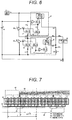
- a main NMOSFET 31 on a high side, a current detection circuit 29 on a high side, a main NMOSFET 33 on a low side, a current detection circuit 30 on a low side, a resistance element 35, a pre-driver 39 on a high side, and a pre-driver 40 on a low side are provided.
- the current detection circuit 29 on the high side includes a sense NMOSFET 32 having a gate electrically connected to a gate of the main MOSFET 31 and a source electrically connected to the source of the main MOSFET 31.
- the drain of the sense NMOSFET 32 and the drain of the main MOSFET 31 are in a virtual short-circuit state by the operational amplifier. Therefore, the current I sH flowing through the sense NMOSFET 32 is a value obtained by multiplying the current I mH flowing through the main NMOSFET 31 by the sense ratio.
- the temperature T mave of the main NMOSFET 31 increases in proportion to the current amount I sH .
- the current detection circuit 30 on the low side includes a sense NMOSFET 34 having a gate electrically connected to a gate of the main MOSFET 33 and a drain electrically connected a drain of the main MOSFET 33.
- the source of the sense NMOSFET 34 and the source of the main MOSFET 33 are in a virtual short-circuit state by the operational amplifier. Therefore, the current I sL flowing through the sense NMOSFET 34 is a value obtained by multiplying the current I mL flowing through the main NMOSFET 33 by the sense ratio.
- the temperature T mave of the main NMOSFET 33 increases in proportion to the current amount I sL .
- the current control device can perform highly precise current control, and is suitable for an automatic transmission control unit (ATCU), an engine control unit (ECU), etc., that control the current of a solenoid.
- ATCU automatic transmission control unit
- ECU engine control unit
Landscapes
- Metal-Oxide And Bipolar Metal-Oxide Semiconductor Integrated Circuits (AREA)
- Element Separation (AREA)
- Thin Film Transistor (AREA)
- Insulated Gate Type Field-Effect Transistor (AREA)
- Semiconductor Integrated Circuits (AREA)
Abstract
Description
- The present invention relates to a current control device such as a current control semiconductor element suitable for detecting an output current of an application specific integrated circuit (ASIC) or the like which outputs a driving current with high accuracy, and an engine control unit (ECU) using the same.
- In order to control an electric actuator such as a motor, and a solenoid with high accuracy, it is necessary to control a driving current with high accuracy. Therefore, it is required to accurately detect the driving current value of the electric actuator.
- One method for detecting a current with high accuracy is to measure a terminal voltage at the time of energization of a shunt resistor using a highly accurate shunt resistor. However, this method has problems of cost increase due to introduction of a shunt resistor, heat generation, and loss of shunt resistance.
- As a method to solve this problem, there is a method in which a sense MOSFET for detecting current is connected in parallel to a main MOSFET that outputs a driving current (see, for example, PTL 1). By setting the gate width of the sense MOSFET to, for example, 1/100 with respect to the main MOSFET, since the current flowing through the sense MOSFET can be 1/100 of the current flowing in the main MOSFET, it is possible to solve the problem of cost increase, heat generation and loss compared to the method using a shunt resistor.
- On the other hand, current detection by the sense MOSFET depends on the accuracy of the current ratio (sense ratio; molecule is the current value of the sense MOSFET and the denominator is the current value of the main MOSFET) of the main MOSFET and the sense MOSFET.
- Here, the main MOSFET and the sense MOSFET generate heat during current driving and the temperature increases. In a general current sense circuit, the voltages at the source, gate and drain terminals of the main MOSFET are set to be the same as the voltages at the respective terminals of the sense MOSFET. The unit MOSFET constituting the main MOSFET and the sense MOSFET has the same structure. For this reason, the power per unit area of the element is the same; however, since the size of the main MOSFET is larger than that of the sense MOSFET, the ratio of the amount of heat dissipation from an element peripheral region to the amount of heat generation becomes smaller. As a result, the temperature of the main MOSFET is higher than the temperature of the sense MOSFET. Here, since the current amount of the MOSFET decreases as the temperature increases, the current reduction rate of the main MOSFET becomes larger than the current reduction rate of the sense MOSFET. As a result, the sense ratio increases as the driving current increases, that is, as the power increases, there arises a problem that the accuracy of current detection decreases.
- In order to solve this problem, as shown in
FIG. 7 , when a part of a multi-finger MOSFET forming themain MOSFET 41 is used as thesense MOSFET 42 and the distance from the center of the multi-finger MOSFET to the furthest channel is L, there is a method of using the channel closest to the position of L/ (√3) from the center of the multi-finger MOSFET as the channel of the sense MOSFET 42 (refer to PTL 2). Here, when the power density in themain MOSFET 41 is uniform, the temperature distribution can be approximated by a quadratic function, and the temperature becomes the highest in the central portion. When the channel current is approximated by the linear equation of the temperature, the distribution of the channel current is expressed by I (x) = αX2 + β ... (1). From this, the average value Iave of the channel current of themain MOSFET 41 is Iave = (1/L) ∫I (x) dx = (α/3)L2 + β ... (2), and becomes equal to the current of the channel of thesense MOSFET 42 located at X = L/(√3). As a result, it is possible to suppress a change in the sense ratio with respect to a change in the driving current of themain MOSFET 41. -
- PTL 1:
JP 2006-203415 A - PTL 2:
JP 2012-9763 A - PTL 3:
JP 2014-44975 A - However, the method of using a part of the multi-finger MOSFET constituting the main MOSFET as the sense MOSFET has the following problems in application.
- First, because the sense MOSFET is disposed in the main MOSFET, the wiring layout of the terminal lead-out of the main MOSFET is restricted by the wiring layout of the lead-out of the source terminal or the drain terminal of the sense MOSFET. In general, since the main MOSFET drives a large current, it is necessary to make a regular wiring layout so as to reduce the influence of the wiring resistance and prevent a local temperature rise. However, due to the presence of the terminal lead-out wiring of the sense MOSFET, the wiring layout of that portion breaks regularity. As a result, there arises a problem that the current density of the wiring layer of the main MOSFET adjacent to the sense MOSFET increases and the parasitic resistance increases.
- Secondly, in the multi-finger MOSFET constituting the main MOSFET, in the case where one of the source and the drain is MOSFET structure electrically connected via the substrate, the configuration of a current detection circuit is restricted. For example, in the current detection circuit provided on the high side shown in
FIG. 2 ofLiterature 3, the drains of the main MOSFET and the sense MOSFET are required to be electrically isolated from each other, this configuration cannot be realized when the mutual drains are electrically connected via the semiconductor substrate. In the current detection circuit provided on the low side, the sources of the main MOSFET and the sense MOSFET are required to be electrically isolated from each other; however, this configuration cannot be realized when the mutual sources are electrically connected via the semiconductor substrate. As described above, the method of using a part of the multi-finger MOSFET as the sense MOSFET is restricted in the circuit configuration. - Thirdly, when the main MOSFET is divided in a gate length direction and a part is used for the sense MOSFET, since a boundary region of division does not operate as a MOSFET, there is a problem that the layout area becomes larger than the case where the main MOSFET is not divided. This problem occurs when the gate width of the sense MOS becomes smaller than the gate width of the multi-finger MOSFET constituting the main MOSFET in order to increase the sense ratio. This increases the layout area of the main MOSFET and increases the chip cost.
- It is an object of the present invention to provide a current control semiconductor element which can suppress a change in sense ratio with respect to a change in driving current of the main MOSFET without causing the above three problems and a current control device using the same.
- A semiconductor element for current control includes: on the same semiconductor substrate, a main MOSFET that drives a current; and a sense MOSFET that is connected in parallel to the main MOSFET and performs current detection of the main MOSFET, wherein the main MOSFET is formed while being surrounded by a first trench groove, the sense MOSFET is formed while being surrounded by a second trench groove, and a thermal conduction coefficient of the first trench groove surrounding the main MOSFET is larger than a thermal conduction coefficient of the second trench groove surrounding the sense MOSFET.
- According to the present invention, a thermal conduction coefficient (λm/tm) derived from the width tm of the trench groove surrounding the main MOSFET and the thermal conductivity λm is set to be larger than a thermal conduction coefficient (λs/ts) derived from a width ts of the trench groove surrounding the sense MOSFET and the thermal conductivity λs. As a result, the amount of heat dissipation per unit length from the trench groove of the sense MOSFET can be made smaller than the amount of heat dissipation per unit length from the trench groove of the main MOSFET. As a result, the difference between the temperature of the main MOSFET and the temperature of the sense MOSFET can be reduced, and the change in the sense ratio with respect to the change in the driving current of the main MOSFET can be suppressed.
-
- [
FIG. 1] FIG. 1 (a) is a plan layout view of a main MOSFET and a sense MOSFET used in a current control semiconductor element according to a first embodiment of the present invention.FIG. 1 (b) is a longitudinal sectional view in a region indicated by A-A' inFIG. 1(a) . - [
FIG. 2] FIG. 2 (a) is a plan layout view of a main MOSFET and a sense MOSFET used in the current control semiconductor element according to the first embodiment of the present invention.FIG. 2(b) is a view showing a temperature distribution in a substrate region indicated by B-B' inFIG. 2(a) . - [
FIG. 3] FIG. 3 is a cross-sectional view of a main MOSFET and a sense MOSFET used for a current control semiconductor element according to a second embodiment of the present invention. - [
FIG. 4] FIG. 4 is a plan layout view of a main MOSFET and a sense MOSFET used in the current control semiconductor element according to a third embodiment of the present invention. - [
FIG. 5] FIG. 5 is a plan layout view of a main MOSFET and a sense MOSFET used in the current control semiconductor element according to a fourth embodiment of the present invention. - [
FIG. 6] FIG. 6 is a circuit diagram of a current control device having a microcontroller that controls the current control semiconductor element according to the first embodiment of the present invention. - [
FIG. 7] FIG. 7 is a plan layout view of a main MOSFET and a sense MOSFET used in a conventional current control semiconductor element. -
- (1) In order to achieve the above purpose, the present invention includes: on the same semiconductor substrate, a main MOSFET that drives a current; and a sense MOSFET that is connected in parallel to the main MOSFET and performs current detection of the main MOSFET, wherein the main MOSFET is formed while being surrounded by a first trench groove, the sense MOSFET is formed while being surrounded by a second trench groove, and a thermal conduction coefficient of the first trench groove surrounding the main MOSFET is larger than a thermal conduction coefficient of the second trench groove surrounding the sense MOSFET. As a result, the amount of heat dissipation per unit length of the first trench groove is made larger than the amount of heat dissipation per unit length of the second trench groove.
- (2) In the above (1), a thermal conductivity of the first trench groove surrounding the main MOSFET is made larger than a thermal conductivity of the second trench groove surrounding the sense MOSFET. As a result, the amount of heat dissipation per unit length of the first trench groove is made larger than the amount of heat dissipation per unit length of the second trench groove.
- (3) In the above (1) or (2), a thermal resistance of the first trench groove surrounding the main MOSFET and a thermal resistance of the second trench groove surrounding the sense MOSFET are inversely proportional to an area of the element region surrounded by the first and second trench grooves. When the power density of the element region is equal, the amount of heat generated by each MOSFET as a whole is proportional to the element area. However, by making the thermal resistance of the trench groove inversely proportional to the device area. Therefore, the amount of heat dissipation from the trench groove is made proportional to the element region so that the difference between the amount of heat generation per unit element area and the amount of heat dissipation is made identical between the main MOSFET and the sense MOSFET.
- (4) In the above (1) to (3), the width of the second trench groove surrounding the sense MOSFET is made larger than the width of the first trench groove surrounding the main MOSFET. As a result, the amount of heat dissipation per unit length of the first trench groove is made larger than the amount of heat dissipation per unit length of the second trench groove.
- (5) In the above (4), a width tm of the first trench groove surrounding the main MOSFET is formed to satisfy tm = α × 2 × (Lm + Wm)/(Lm × Wm) with respect to a length Lm and width Wm of the main MOSFET. A width ts of the second trench groove surrounding the sense MOSFET is formed to satisfy ts = α × 2 × (L, + Ws)/(Ls × Ws) with respect to a length Ls and a width Ws of the sense MOSFET. Accordingly, when a thermal conductivity of the film buried in the first trench groove and the second trench groove is the same, the thermal resistance of the first trench groove surrounding the main MOSFET and the thermal resistance of the second trench groove surrounding the sense MOSFET are inversely proportional to the area of the element region surrounded by the first and second trench grooves.
- (6) In the above (2) to (5), the first trench groove surrounding the main MOSFET is formed of one or a plurality of trench grooves, the second trench groove surrounding the sense MOSFET is formed of a plurality of trench grooves, and the number of the first trench grooves surrounding the main MOSFET is set to be smaller than the number of the second trench grooves surrounding the sense MOSFET.
- (7) In each of the above (1) to (6), each of the main MOSFET and the sense MOSFET has a multi-finger MOSFET structure in which a plurality of channels are arranged in a line at equal intervals, and the channel intervals of the main MOSFET and the sense MOSFET are formed to be equal to each other.
- (8) In the above (4) to (6), the main MOSFET and the sense MOSFET are formed so as to be adjacent to each other via the first trench groove.
- (9) In the above (1) to (8), it is preferable that the current control semiconductor element is mounted on an ASIC that outputs a driving current.
- (10) In order to achieve the above purpose, the present invention is a current control device including: a current control semiconductor element; and a microcontroller that controls the current control semiconductor element, wherein the current control semiconductor element includes: on the same semiconductor substrate, a main MOSFET that drives a current; and a sense MOSFET that is connected in parallel to the main MOSFET and performs current detection of the main MOSFET, wherein the main MOSFET is formed while being surrounded by a first trench groove, the sense MOSFET is formed while being surrounded by a second trench groove, and a thermal resistance of the second trench groove surrounding the main MOSFET is larger than a thermal resistance of the first trench groove surrounding the sense MOSFET.
- With such a configuration, the temperature difference between the sense MOSFET and the main MOSFET can be reduced, and the change in the sense ratio with respect to the change in the driving current of the main MOSFET can be suppressed. As a result, the accuracy of current detection by the sense MOSFET can be improved.
- According to the present invention, a thermal conduction coefficient (λm/tm) derived from the width tm of the trench groove surrounding the main MOSFET and the thermal conductivity λm is set to be larger than a thermal conduction coefficient (λs/ts) derived from a width ts of the trench groove surrounding the sense MOSFET and the thermal conductivity λs. As a result, the amount of heat dissipation per unit length from the trench groove of the sense MOSFET can be made smaller than the amount of heat dissipation per unit length from the trench groove of the main MOSFET. As a result, the difference between the temperature of the main MOSFET and the temperature of the sense MOSFET can be reduced, and the change in the sense ratio with respect to the change in the driving current of the main MOSFET can be suppressed.
- Further, according to the present invention, the thermal conductivity λm of the trench groove surrounding the main MOSFET is made larger than the thermal conductivity λs of the trench groove surrounding the sense MOSFET. As a result, the amount of heat dissipation per unit length from the trench groove of the sense MOSFET can be made smaller than the amount of heat dissipation per unit length from the trench groove of the main MOSFET. As a result, the difference between the average temperature of the main MOSFET and the average temperature of the sense MOSFET can be reduced, and the change in the sense ratio with respect to the change in the driving current of the main MOSFET can be suppressed.
- Further, according to the present invention, the groove width tm of the trench groove surrounding the main MOSFET is made larger than the groove width ts of the trench groove surrounding the sense MOSFET. As a result, similarly, the amount of heat dissipation per unit length from the trench groove of the sense MOSFET can be made smaller than the amount of heat dissipation per unit length from the trench groove of the main MOSFET. As a result, the difference between the average temperature of the main MOSFET and the average temperature of the sense MOSFET can be reduced, and the change in the sense ratio with respect to the change in the driving current of the main MOSFET can be suppressed.
- Further, according to the present invention, the thermal resistance Rthm of the trench groove surrounding the main MOSFET and the thermal resistance Rths of the trench groove surrounding the sense MOSFET are formed so as to be inversely proportional to the area of the semiconductor element region surrounded by each trench groove. Accordingly, the amount of heat dissipation from the trench groove can be proportional to the area of the semiconductor element region. As a result, the difference between the amount of heat generation per unit area of the semiconductor element region and the amount of heat dissipation can be made identical between the main MOSFET and the sense MOSFET, and the temperature difference of the MOSFET can be further reduced. Therefore, it is possible to further suppress the change in the sense ratio with respect to the change in the driving current of the main MOSFET.
- Further, according to the present invention, the sense MOSFET and the main MOSFET have a multi-finger MOSFET structure having the same channel spacing, and by surrounding each with a trench groove, regular pattern arrangement is possible without restriction on the wiring layout of the main MOSFET.
- Further, according to the present invention, the sense MOSFET and the main MOSFET are isolated from each other by surrounding each of the sense MOSFET and the main MOSFET with a trench groove. Therefore, in the multi-finger MOSFET, it is possible to eliminate the restriction that the source and drain of the sense MOSFET and the main MOSFET are electrically connected via the substrate.
- Further, according to the present invention, since the sense MOSFET and the main MOSFET are each surrounded by a trench groove, the size of the sense MOSFET does not affect the size of the main MOSFET. That is, when the sense ratio is small, it is possible to eliminate the problem that the main MOSFET is divided in the gate length direction to reduce the layout area efficiency of the main MOSFET. Hereinafter, embodiments of the present invention will be described with reference to the drawings. Although the case of using the NMOSFET is described in this embodiment, it may be a PMOSFET. Further, in this embodiment, the MOSFET is formed on an SOI substrate, but a Si substrate may be used. (First Embodiment)The first embodiment of the present invention will be described with reference to
FIGS. 1 and 2. FIG. 1(a) is a plan layout view of amain MOSFET 1 and asense MOSFET 2 used in a current control semiconductor element according to the present embodiment.FIG. 1(b) shows a longitudinal sectional view in a region indicated by A-A' inFIG. 1(a) . - Both the
main MOSFET 1 and thesense MOSFET 2 have a multi-finger MOSFET structure in which a plurality of channels are arranged in a line at equal intervals. The MOSFET has a Lateral Double Diffused MOS (LDMOS) structure in which an electric field strength betweendrains gates main MOSFET 1 is surrounded by atrench groove 13 in which an insulatingfilm 3 is buried, and thesense MOSFET 2 is surrounded by atrench groove 14 in which an insulatingfilm 4 is buried. The insulatingfilm 3 and the insulatingfilm 4 are made of SiO2 film, and a width tm of thetrench groove 13 is smaller than a width ts of thetrench groove 14. Here, the thermal conduction coefficient of the trench groove is expressed as λ/t using the thermal conductivity λ of the SiO2 film and the width t of the trench groove. Accordingly, the thermal conduction coefficient (λ/tm) of thetrench groove 13 is larger than the thermal conduction coefficient (λ/ts) of thetrench groove 14. This means that the amount of heat dissipation per unit length of the trench groove is larger in thetrench groove 13 than in thetrench groove 14. - Next, the junction temperature of the
main MOSFET 1 and thesense MOSFET 2 during current driving of themain MOSFET 1 will be described with reference toFIG. 2. FIG. 2 (a) is the same asFIG. 1(a) and shows a plan layout view, andFIG. 2(b) shows the temperature in the region indicated by B-B'. A temperature at the center of the main MOSFET is Tmmax, a temperature at the end portion is Tmmin, an average temperature is Tmave, a temperature at the center portion of the sense MOSFET is Tsmax, a temperature at the end portion is Tsmin, and an average temperature is Tsave. - In the case where the
main MOSFET 1 and thesense MOSFET 2 are operating at a uniform power density in the semiconductor element region, the temperature in the Si device region surrounded by thetrench grooves trench grooves main MOSFET 1 having a larger area of the Si device region. In the present invention, by making the thermal conduction coefficient of thetrench groove 13 larger than that of thetrench groove 14, the amount of heat dissipation from thetrench groove 14 of thesense MOSFET 2 is relatively reduced, so that a temperature Tsave of thesense MOSFET 2 is made to approach a temperature Tmave of themain MOSFET 1. As a result, it is possible to further suppress the change in the sense ratio with respect to the change in the driving current of the main MOSFET. - Further, the widths of the
trench grooves main MOSFET 1 and thesense MOSFET 2. As a result, it is possible to further suppress the change in the sense ratio with respect to the change in the driving current of the main MOSFET. - Although the insulating
film 3 and the insulatingfilm 4 are made of SiO2 film in this embodiment, it is not necessary that they are made of the same material, and may be formed of different materials so that the thermal conductivity λm of thetrench groove 13 is larger than the thermal conductivity λs of thetrench groove 14. As a result, even when the width tm of thetrench groove 13 and the width ts of thetrench groove 14 are the same, the thermal conduction coefficient (λm/tm) of thetrench groove 13 can be made larger than the thermal conduction coefficient (AS/ts) of thetrench groove 14, and the same effect can be obtained. (Second Embodiment)The second embodiment of the present invention will be described with reference toFIG. 3. FIG. 3 shows a cross-sectional view of a semiconductor element according to the present invention. Amain MOSFET 1 is surrounded by atrench groove 13 and asense MOSFET 2 is surrounded by atrench groove 14. Thetrench groove 13 is formed by embedding a SiO2 film 3, thetrench groove 14 is partially embedded with the SiO2 film 4, and agap 28 is formed in a part thereof. - Since the thermal conductivity of the
gap 28 of thetrench groove 14 is smaller than that of the SiO2 film, the thermal conductivity λm of thetrench groove 13 is larger than the thermal conductivity λs of thetrench groove 14. As a result, the thermal conduction coefficient λm/tm of thetrench groove 13 is larger than the thermal conduction coefficient λs/ts of thetrench groove 14. This indicates that the amount of heat dissipation per unit length of the trench groove is larger in thetrench groove 13 than in thetrench groove 14. Accordingly, the amount of heat dissipation from thetrench groove 14 of thesense MOSFET 2 is relatively reduced, so that a temperature Tsave of thesense MOSFET 2 is made to approach a temperature Tmave of themain MOSFET 1. - Further, the
trench groove 13 is formed so that the thermal conduction coefficient λm/tm of thetrench groove 13 becomes λm/tm = β × Lm × Wm/ {2 × (Lm + Wm) }. Thetrench groove 14 is formed so that the thermal conduction coefficient λs/ts of thetrench groove 14 becomes λs/ts = β × Ls × Ws/{2 × (Ls+Ws)}. Since the thermal resistance Rth of the trench groove is derived by dividing the reciprocal of the thermal conduction coefficient by the cross sectional area of the trench groove {2 × (L + W) × tSi}, the thermal resistance Rthm of thetrench groove 13 and the thermal resistance Rths of thetrench groove 14 are Rthm = 1/ (β × Lm × Wm × tSi) Rths = 1/(β × Ls × Ws × tSi). Therefore, the thermal resistance of thetrench grooves main MOSFET 1 and thesense MOSFET 2 is also proportional to the area (L × W) of the semiconductor element region, the average temperature Tave determined by the difference between the amount of heat generation and the amount of heat dissipation can be made identical between themain MOSFET 1 and thesense MOSFET 2. As a result, it is possible to further suppress the change in the sense ratio with respect to the change in the driving current of the main MOSFET. (Third Embodiment)The third embodiment of the present invention will be described with reference toFIG. 4. FIG. 4 shows a plan view of a semiconductor element according to the present invention. Amain MOSFET 1 is surrounded by onetrench groove 13 and asense MOSFET 2 is surrounded by twotrench grooves trench groove 13 is formed to be smaller than the total value of the widths tsa, tsa of thetrench grooves trench groove 13, the amount of heat dissipation per unit length from thetrench groove 14 can be suppressed as compared with thetrench groove 13. As a result, the temperature Tsave of thesense MOSFET 2 at the time of current driving can be made to approach the temperature Tmave of themain MOSFET 1. - The number of trench grooves is not limited to this, the above object can be satisfied if the total value of the widths of all the trench grooves constituting the
trench groove 13 is smaller than the total value of the widths of all the trench grooves constituting thetrench groove 14. - As described in the first and second embodiments, it is not necessary to fill the
trench groove 13 and thetrench grooves trench groove 13 is larger than the thermal conduction coefficient of thetrench grooves FIG. 5. FIG. 5 shows a plan view of a semiconductor device according to the present invention. Amain MOSFET 1 is surrounded by atrench groove 13 and asense MOSFET 2 is surrounded by atrench groove 14. Themain MOSFET 1 and thesense MOSFET 2 are in contact with each other via thetrench groove 14. By sharing part of the trench groove, the layout area can be reduced, and the temperature Tsave of the sense MOSFET can be raised relatively by heat radiation from the main MOSFET. As a result, the temperature Tsave of thesense MOSFET 2 at the time of current driving can be brought close to the temperature Tmave of themain MOSFET 1, and the change of the sense ratio with respect to the change of the driving current of the main MOSFET can be suppressed. (Fifth Embodiment)The fifth embodiment of the present invention will be described with reference toFIG. 6. FIG. 6 shows a circuit structure of a current control device having a microcontroller that controls a semiconductor element according to the present invention. This circuit is used for a linear solenoid driver when, for example, a linear solenoid is used as anelectromagnetic load 36. A main NMOSFET 31 on a high side, acurrent detection circuit 29 on a high side, amain NMOSFET 33 on a low side, acurrent detection circuit 30 on a low side, aresistance element 35, a pre-driver 39 on a high side, and a pre-driver 40 on a low side are provided. - The
current detection circuit 29 on the high side includes asense NMOSFET 32 having a gate electrically connected to a gate of the main MOSFET 31 and a source electrically connected to the source of the main MOSFET 31. On the other hand, the drain of thesense NMOSFET 32 and the drain of the main MOSFET 31 are in a virtual short-circuit state by the operational amplifier. Therefore, the current IsH flowing through thesense NMOSFET 32 is a value obtained by multiplying the current ImH flowing through the main NMOSFET 31 by the sense ratio. The temperature Tmave of the main NMOSFET 31 increases in proportion to the current amount IsH. However, according to the configuration of the present invention, by suppressing the heat dissipation from the trench groove of thesense NMOSFET 32 and reducing the temperature difference between the main NMOSFET 31 and thesense NMOSFET 32, it is possible to suppress the change in the sense ratio with respect to the change in the driving current of the main MOSFET 31. - Similarly, the
current detection circuit 30 on the low side includes asense NMOSFET 34 having a gate electrically connected to a gate of themain MOSFET 33 and a drain electrically connected a drain of themain MOSFET 33. On the other hand, the source of thesense NMOSFET 34 and the source of themain MOSFET 33 are in a virtual short-circuit state by the operational amplifier. Therefore, the current IsL flowing through thesense NMOSFET 34 is a value obtained by multiplying the current ImL flowing through themain NMOSFET 33 by the sense ratio. The temperature Tmave of themain NMOSFET 33 increases in proportion to the current amount IsL. However, according to the configuration of the present embodiment, by suppressing the heat dissipation from the trench groove of thesense NMOSFET 34 and reducing the temperature difference between themain NMOSFET 33 and thesense NMOSFET 34, it is possible to suppress the change in the sense ratio with respect to the change in the driving current of themain MOSFET 33. As a result, the current control device can perform highly precise current control, and is suitable for an automatic transmission control unit (ATCU), an engine control unit (ECU), etc., that control the current of a solenoid. -
- 1
- main MOSFET
- 2
- sense MOSFET
- 3
- first insulating film
- 4
- second insulating film
- 5
- main MOSFET source
- 6
- main MOSFET gate
- 7
- main MOSFET drain
- 8
- source MOSFET source
- 9
- source MOSFET gate
- 10
- source MOSFET drain
- 11
- SOI layer
- 12
- semiconductor substrate
- 13
- trench groove surrounding main MOSFET
- 14
- trench groove surrounding sense MOSFET
- 15
- STI trench
- 16
- main MOSFET P-body layer
- 17
- main MOSFET P-body connection P+layer
- 18
- main MOSFET source N+layer
- 19
- main MOSFET drain N+layer
- 20
- sense MOSFET P-body layer
- 21
- sense MOSFET P-body connection P+layer
- 22
- sense MOSFET source N+layer
- 23
- sense MOSFET drain N+layer
- 24
- contact
- 25
- wiring first layer
- 26
- wiring connection layer
- 27
- wiring second layer
- 28
- gap
- 29
- current detection circuit at high side
- 30
- current detection circuit at low side
- 31
- main NMOSFET at high side
- 32
- sense NMOSFET at high side
- 33
- main NMOSFET at low side
- 34
- sense NMOSFET at low side
- 35
- resistance element
- 36
- electromagnetic load
- 37
- boost circuit
- 38
- power supply
- 39
- pre-driver at high side
- 40
- pre-driver at low side
- 41
- main MOSFET
- 42
- sense MOSFET
- 43
- gate lead-out wiring first layer
- 44
- sense MOSFET drain lead-out wiring second layer
- 45
- main MOSFET drain lead-out wiring third layer
- 46
- MOSFET common source lead-out wiring third layer
Claims (10)
- A semiconductor element for current control comprising: on the same semiconductor substrate, a main MOSFET that drives a current; and a sense MOSFET that is connected in parallel to the main MOSFET and performs current detection of the main MOSFET, wherein
the main MOSFET is formed while being surrounded by a first trench groove,
the sense MOSFET is formed while being surrounded by a second trench groove, and
a thermal conduction coefficient of the first trench groove surrounding the main MOSFET is larger than a thermal conduction coefficient of the second trench groove surrounding the sense MOSFET. - The semiconductor element for current control according to claim 1, wherein
a thermal conductivity of the first trench groove surrounding the main MOSFET is made larger than a thermal conductivity of the second trench groove surrounding the sense MOSFET. - The semiconductor element for current control according to claim 2, wherein
a width of the first trench groove surrounding the main MOSFET is made larger than a width of the second trench groove surrounding the sense MOSFET. - The semiconductor element for current control according to claim 3, wherein
a thermal resistance of the first trench groove surrounding the main MOSFET and a thermal resistance of the second trench groove surrounding the sense MOSFET are inversely proportional to an area of the element region surrounded by the first and second trench grooves. - The semiconductor element for current control according to claim 4, wherein
a width tm of the first trench groove surrounding the main MOSFET is formed to satisfy a relationship of tm = α × 2 × (Lm + Wm)/(Lm × Wm) with respect to a length Lm and width Wm of the semiconductor element region surrounded by the first trench groove, and
a width ts of the second trench groove surrounding the sense MOSFET is formed to satisfy a relationship of ts = α × 2 × (Ls + Ws) /(Ls × Ws) with respect to a length Ls and the width Ws of the semiconductor element region surrounded by the second trench groove. - The semiconductor element for current control according to claim 2, wherein
the first trench groove surrounding the main MOSFET is formed of one or a plurality of trench grooves,
the second trench groove surrounding the sense MOSFET is formed of a plurality of trench grooves, and
the number of the first trench grooves surrounding the main MOSFET is set to be smaller than the number of the second trench grooves surrounding the sense MOSFET. - The semiconductor element for current control according to claim 1, wherein
the main MOSFET has a structure in which a plurality of channels are arranged in a line at equal intervals,
the sense MOSFET has a structure in which a plurality of channels are arranged in a line at equal intervals, and
an interval between channels of the main MOSFET is equal to an interval between channels of the sense MOSFET. - The semiconductor element for current control according to claim 1, wherein
the main MOSFET and the sense MOSFET are arranged adjacent to each other via the first trench groove or the second trench groove. - The semiconductor element for current control according to claim 1, wherein
the semiconductor element for current control is mounted on an application specific integrated circuit (ASIC) which outputs a driving current. - A current control device comprising:a current control semiconductor element; anda microcontroller that controls the current control semiconductor element, whereinthe current control semiconductor element includes: on the same semiconductor substrate, a main MOSFET that drives a current; and a sense MOSFET that is connected in parallel to the main MOSFET and performs current detection of the main MOSFET, whereinthe main MOSFET is formed while being surrounded by a first trench groove,the sense MOSFET is formed while being surrounded by a second trench groove, anda thermal conduction coefficient of the first trench groove surrounding the main MOSFET is larger than a thermal conduction coefficient of the second trench groove surrounding the sense MOSFET.
Applications Claiming Priority (2)
| Application Number | Priority Date | Filing Date | Title |
|---|---|---|---|
| JP2015011930A JP6430269B2 (en) | 2015-01-26 | 2015-01-26 | Semiconductor device for current control and current control device using the same |
| PCT/JP2016/050423 WO2016121452A1 (en) | 2015-01-26 | 2016-01-08 | Current control semiconductor element and current control device using same |
Publications (3)
| Publication Number | Publication Date |
|---|---|
| EP3252815A1 true EP3252815A1 (en) | 2017-12-06 |
| EP3252815A4 EP3252815A4 (en) | 2018-08-29 |
| EP3252815B1 EP3252815B1 (en) | 2022-06-15 |
Family
ID=56543072
Family Applications (1)
| Application Number | Title | Priority Date | Filing Date |
|---|---|---|---|
| EP16743056.0A Active EP3252815B1 (en) | 2015-01-26 | 2016-01-08 | Current control semiconductor element and current control device using same |
Country Status (3)
| Country | Link |
|---|---|
| EP (1) | EP3252815B1 (en) |
| JP (1) | JP6430269B2 (en) |
| WO (1) | WO2016121452A1 (en) |
Cited By (1)
| Publication number | Priority date | Publication date | Assignee | Title |
|---|---|---|---|---|
| WO2025106483A1 (en) * | 2023-11-16 | 2025-05-22 | Wolfspeed, Inc. | Enhanced isolation for on-chip current sensors |
Families Citing this family (1)
| Publication number | Priority date | Publication date | Assignee | Title |
|---|---|---|---|---|
| JP2023131415A (en) * | 2022-03-09 | 2023-09-22 | ルネサスエレクトロニクス株式会社 | semiconductor equipment |
Family Cites Families (7)
| Publication number | Priority date | Publication date | Assignee | Title |
|---|---|---|---|---|
| JPH0574802A (en) * | 1991-04-26 | 1993-03-26 | Toyota Autom Loom Works Ltd | Transistor having current detecting function |
| US6180966B1 (en) * | 1997-03-25 | 2001-01-30 | Hitachi, Ltd. | Trench gate type semiconductor device with current sensing cell |
| JP2000022140A (en) * | 1998-06-26 | 2000-01-21 | Nissan Motor Co Ltd | Semiconductor device and manufacturing method thereof |
| JP2000217347A (en) * | 1999-01-22 | 2000-08-04 | Nissan Motor Co Ltd | Current control circuit |
| JP5367651B2 (en) * | 2010-06-28 | 2013-12-11 | 日立オートモティブシステムズ株式会社 | Semiconductor device for current control and control device using the same |
| JP6037499B2 (en) * | 2011-06-08 | 2016-12-07 | ローム株式会社 | Semiconductor device and manufacturing method thereof |
| JP2014187082A (en) * | 2013-03-22 | 2014-10-02 | Hitachi Ltd | Semiconductor device |
-
2015
- 2015-01-26 JP JP2015011930A patent/JP6430269B2/en active Active
-
2016
- 2016-01-08 WO PCT/JP2016/050423 patent/WO2016121452A1/en not_active Ceased
- 2016-01-08 EP EP16743056.0A patent/EP3252815B1/en active Active
Cited By (1)
| Publication number | Priority date | Publication date | Assignee | Title |
|---|---|---|---|---|
| WO2025106483A1 (en) * | 2023-11-16 | 2025-05-22 | Wolfspeed, Inc. | Enhanced isolation for on-chip current sensors |
Also Published As
| Publication number | Publication date |
|---|---|
| EP3252815A4 (en) | 2018-08-29 |
| JP6430269B2 (en) | 2018-11-28 |
| WO2016121452A1 (en) | 2016-08-04 |
| JP2016139631A (en) | 2016-08-04 |
| EP3252815B1 (en) | 2022-06-15 |
Similar Documents
| Publication | Publication Date | Title |
|---|---|---|
| CN103918084A (en) | Semiconductor device | |
| US20040222461A1 (en) | Lateral semiconductor device with low on-resistance and method of making the same | |
| KR102528685B1 (en) | Power semiconductor devices having different gate crossings and method for manufacturing thereof | |
| US8963241B1 (en) | Integrated MOS power transistor with poly field plate extension for depletion assist | |
| US8969958B1 (en) | Integrated MOS power transistor with body extension region for poly field plate depletion assist | |
| CN103928463A (en) | High-voltage ED NMOS element embedded high-voltage transverse NJFET | |
| EP3252815B1 (en) | Current control semiconductor element and current control device using same | |
| CN114556588B (en) | Switching element | |
| US7187034B2 (en) | Distributed power MOSFET | |
| JP7256771B2 (en) | semiconductor equipment | |
| CN108140611B (en) | Switching element and load driving device | |
| US11145646B2 (en) | Semiconductor device | |
| Wessels | Smart power technologies on SOI | |
| US9602099B2 (en) | Adaptive duo-gate MOSFET | |
| US9331158B2 (en) | Transistor devices and methods | |
| KR101437275B1 (en) | Semiconductor device having a multi floating island | |
| US20090236659A1 (en) | Isolation structure for semiconductor device with multiple terminals | |
| US20110156141A1 (en) | Transistor and method thereof | |
| CN104916696A (en) | Semiconductor device | |
| EP1870940A1 (en) | Semiconductor device | |
| US11967624B2 (en) | Semiconductor device | |
| KR101262643B1 (en) | Multi transistor | |
| CN108352359B (en) | semiconductor device | |
| US7732833B2 (en) | High-voltage semiconductor switching element | |
| JP2016072532A (en) | Semiconductor element |
Legal Events
| Date | Code | Title | Description |
|---|---|---|---|
| STAA | Information on the status of an ep patent application or granted ep patent |
Free format text: STATUS: THE INTERNATIONAL PUBLICATION HAS BEEN MADE |
|
| PUAI | Public reference made under article 153(3) epc to a published international application that has entered the european phase |
Free format text: ORIGINAL CODE: 0009012 |
|
| STAA | Information on the status of an ep patent application or granted ep patent |
Free format text: STATUS: REQUEST FOR EXAMINATION WAS MADE |
|
| 17P | Request for examination filed |
Effective date: 20170828 |
|
| AK | Designated contracting states |
Kind code of ref document: A1 Designated state(s): AL AT BE BG CH CY CZ DE DK EE ES FI FR GB GR HR HU IE IS IT LI LT LU LV MC MK MT NL NO PL PT RO RS SE SI SK SM TR |
|
| AX | Request for extension of the european patent |
Extension state: BA ME |
|
| DAV | Request for validation of the european patent (deleted) | ||
| DAX | Request for extension of the european patent (deleted) | ||
| A4 | Supplementary search report drawn up and despatched |
Effective date: 20180801 |
|
| RIC1 | Information provided on ipc code assigned before grant |
Ipc: H01L 27/088 20060101ALI20180726BHEP Ipc: H01L 21/8234 20060101AFI20180726BHEP Ipc: H01L 29/786 20060101ALI20180726BHEP Ipc: H01L 27/12 20060101ALN20180726BHEP Ipc: H01L 27/02 20060101ALN20180726BHEP Ipc: H01L 29/78 20060101ALI20180726BHEP |
|
| STAA | Information on the status of an ep patent application or granted ep patent |
Free format text: STATUS: EXAMINATION IS IN PROGRESS |
|
| 17Q | First examination report despatched |
Effective date: 20210129 |
|
| RAP3 | Party data changed (applicant data changed or rights of an application transferred) |
Owner name: HITACHI ASTEMO, LTD. |
|
| REG | Reference to a national code |
Ref country code: DE Ref legal event code: R079 Ref document number: 602016072848 Country of ref document: DE Free format text: PREVIOUS MAIN CLASS: H01L0027080000 Ipc: H01L0021823400 |
|
| GRAP | Despatch of communication of intention to grant a patent |
Free format text: ORIGINAL CODE: EPIDOSNIGR1 |
|
| STAA | Information on the status of an ep patent application or granted ep patent |
Free format text: STATUS: GRANT OF PATENT IS INTENDED |
|
| RIC1 | Information provided on ipc code assigned before grant |
Ipc: H01L 27/12 20060101ALN20220309BHEP Ipc: H01L 27/02 20060101ALN20220309BHEP Ipc: H01L 29/06 20060101ALI20220309BHEP Ipc: H01L 29/78 20060101ALI20220309BHEP Ipc: H01L 27/088 20060101ALI20220309BHEP Ipc: H01L 21/8234 20060101AFI20220309BHEP |
|
| INTG | Intention to grant announced |
Effective date: 20220407 |
|
| GRAS | Grant fee paid |
Free format text: ORIGINAL CODE: EPIDOSNIGR3 |
|
| GRAA | (expected) grant |
Free format text: ORIGINAL CODE: 0009210 |
|
| STAA | Information on the status of an ep patent application or granted ep patent |
Free format text: STATUS: THE PATENT HAS BEEN GRANTED |
|
| AK | Designated contracting states |
Kind code of ref document: B1 Designated state(s): AL AT BE BG CH CY CZ DE DK EE ES FI FR GB GR HR HU IE IS IT LI LT LU LV MC MK MT NL NO PL PT RO RS SE SI SK SM TR |
|
| REG | Reference to a national code |
Ref country code: CH Ref legal event code: EP Ref country code: GB Ref legal event code: FG4D |
|
| REG | Reference to a national code |
Ref country code: IE Ref legal event code: FG4D |
|
| REG | Reference to a national code |
Ref country code: DE Ref legal event code: R096 Ref document number: 602016072848 Country of ref document: DE |
|
| REG | Reference to a national code |
Ref country code: AT Ref legal event code: REF Ref document number: 1498892 Country of ref document: AT Kind code of ref document: T Effective date: 20220715 |
|
| REG | Reference to a national code |
Ref country code: LT Ref legal event code: MG9D |
|
| REG | Reference to a national code |
Ref country code: NL Ref legal event code: MP Effective date: 20220615 |
|
| PG25 | Lapsed in a contracting state [announced via postgrant information from national office to epo] |
Ref country code: SE Free format text: LAPSE BECAUSE OF FAILURE TO SUBMIT A TRANSLATION OF THE DESCRIPTION OR TO PAY THE FEE WITHIN THE PRESCRIBED TIME-LIMIT Effective date: 20220615 Ref country code: NO Free format text: LAPSE BECAUSE OF FAILURE TO SUBMIT A TRANSLATION OF THE DESCRIPTION OR TO PAY THE FEE WITHIN THE PRESCRIBED TIME-LIMIT Effective date: 20220915 Ref country code: LT Free format text: LAPSE BECAUSE OF FAILURE TO SUBMIT A TRANSLATION OF THE DESCRIPTION OR TO PAY THE FEE WITHIN THE PRESCRIBED TIME-LIMIT Effective date: 20220615 Ref country code: HR Free format text: LAPSE BECAUSE OF FAILURE TO SUBMIT A TRANSLATION OF THE DESCRIPTION OR TO PAY THE FEE WITHIN THE PRESCRIBED TIME-LIMIT Effective date: 20220615 Ref country code: GR Free format text: LAPSE BECAUSE OF FAILURE TO SUBMIT A TRANSLATION OF THE DESCRIPTION OR TO PAY THE FEE WITHIN THE PRESCRIBED TIME-LIMIT Effective date: 20220916 Ref country code: FI Free format text: LAPSE BECAUSE OF FAILURE TO SUBMIT A TRANSLATION OF THE DESCRIPTION OR TO PAY THE FEE WITHIN THE PRESCRIBED TIME-LIMIT Effective date: 20220615 Ref country code: BG Free format text: LAPSE BECAUSE OF FAILURE TO SUBMIT A TRANSLATION OF THE DESCRIPTION OR TO PAY THE FEE WITHIN THE PRESCRIBED TIME-LIMIT Effective date: 20220915 |
|
| REG | Reference to a national code |
Ref country code: AT Ref legal event code: MK05 Ref document number: 1498892 Country of ref document: AT Kind code of ref document: T Effective date: 20220615 |
|
| PG25 | Lapsed in a contracting state [announced via postgrant information from national office to epo] |
Ref country code: RS Free format text: LAPSE BECAUSE OF FAILURE TO SUBMIT A TRANSLATION OF THE DESCRIPTION OR TO PAY THE FEE WITHIN THE PRESCRIBED TIME-LIMIT Effective date: 20220615 Ref country code: LV Free format text: LAPSE BECAUSE OF FAILURE TO SUBMIT A TRANSLATION OF THE DESCRIPTION OR TO PAY THE FEE WITHIN THE PRESCRIBED TIME-LIMIT Effective date: 20220615 |
|
| PG25 | Lapsed in a contracting state [announced via postgrant information from national office to epo] |
Ref country code: NL Free format text: LAPSE BECAUSE OF FAILURE TO SUBMIT A TRANSLATION OF THE DESCRIPTION OR TO PAY THE FEE WITHIN THE PRESCRIBED TIME-LIMIT Effective date: 20220615 |
|
| PG25 | Lapsed in a contracting state [announced via postgrant information from national office to epo] |
Ref country code: SM Free format text: LAPSE BECAUSE OF FAILURE TO SUBMIT A TRANSLATION OF THE DESCRIPTION OR TO PAY THE FEE WITHIN THE PRESCRIBED TIME-LIMIT Effective date: 20220615 Ref country code: SK Free format text: LAPSE BECAUSE OF FAILURE TO SUBMIT A TRANSLATION OF THE DESCRIPTION OR TO PAY THE FEE WITHIN THE PRESCRIBED TIME-LIMIT Effective date: 20220615 Ref country code: RO Free format text: LAPSE BECAUSE OF FAILURE TO SUBMIT A TRANSLATION OF THE DESCRIPTION OR TO PAY THE FEE WITHIN THE PRESCRIBED TIME-LIMIT Effective date: 20220615 Ref country code: PT Free format text: LAPSE BECAUSE OF FAILURE TO SUBMIT A TRANSLATION OF THE DESCRIPTION OR TO PAY THE FEE WITHIN THE PRESCRIBED TIME-LIMIT Effective date: 20221017 Ref country code: ES Free format text: LAPSE BECAUSE OF FAILURE TO SUBMIT A TRANSLATION OF THE DESCRIPTION OR TO PAY THE FEE WITHIN THE PRESCRIBED TIME-LIMIT Effective date: 20220615 Ref country code: EE Free format text: LAPSE BECAUSE OF FAILURE TO SUBMIT A TRANSLATION OF THE DESCRIPTION OR TO PAY THE FEE WITHIN THE PRESCRIBED TIME-LIMIT Effective date: 20220615 Ref country code: CZ Free format text: LAPSE BECAUSE OF FAILURE TO SUBMIT A TRANSLATION OF THE DESCRIPTION OR TO PAY THE FEE WITHIN THE PRESCRIBED TIME-LIMIT Effective date: 20220615 Ref country code: AT Free format text: LAPSE BECAUSE OF FAILURE TO SUBMIT A TRANSLATION OF THE DESCRIPTION OR TO PAY THE FEE WITHIN THE PRESCRIBED TIME-LIMIT Effective date: 20220615 |
|
| PG25 | Lapsed in a contracting state [announced via postgrant information from national office to epo] |
Ref country code: PL Free format text: LAPSE BECAUSE OF FAILURE TO SUBMIT A TRANSLATION OF THE DESCRIPTION OR TO PAY THE FEE WITHIN THE PRESCRIBED TIME-LIMIT Effective date: 20220615 Ref country code: IS Free format text: LAPSE BECAUSE OF FAILURE TO SUBMIT A TRANSLATION OF THE DESCRIPTION OR TO PAY THE FEE WITHIN THE PRESCRIBED TIME-LIMIT Effective date: 20221015 |
|
| REG | Reference to a national code |
Ref country code: DE Ref legal event code: R097 Ref document number: 602016072848 Country of ref document: DE |
|
| PG25 | Lapsed in a contracting state [announced via postgrant information from national office to epo] |
Ref country code: AL Free format text: LAPSE BECAUSE OF FAILURE TO SUBMIT A TRANSLATION OF THE DESCRIPTION OR TO PAY THE FEE WITHIN THE PRESCRIBED TIME-LIMIT Effective date: 20220615 |
|
| PLBE | No opposition filed within time limit |
Free format text: ORIGINAL CODE: 0009261 |
|
| STAA | Information on the status of an ep patent application or granted ep patent |
Free format text: STATUS: NO OPPOSITION FILED WITHIN TIME LIMIT |
|
| PG25 | Lapsed in a contracting state [announced via postgrant information from national office to epo] |
Ref country code: DK Free format text: LAPSE BECAUSE OF FAILURE TO SUBMIT A TRANSLATION OF THE DESCRIPTION OR TO PAY THE FEE WITHIN THE PRESCRIBED TIME-LIMIT Effective date: 20220615 |
|
| 26N | No opposition filed |
Effective date: 20230316 |
|
| PG25 | Lapsed in a contracting state [announced via postgrant information from national office to epo] |
Ref country code: SI Free format text: LAPSE BECAUSE OF FAILURE TO SUBMIT A TRANSLATION OF THE DESCRIPTION OR TO PAY THE FEE WITHIN THE PRESCRIBED TIME-LIMIT Effective date: 20220615 |
|
| REG | Reference to a national code |
Ref country code: CH Ref legal event code: PL |
|
| GBPC | Gb: european patent ceased through non-payment of renewal fee |
Effective date: 20230108 |
|
| PG25 | Lapsed in a contracting state [announced via postgrant information from national office to epo] |
Ref country code: LU Free format text: LAPSE BECAUSE OF NON-PAYMENT OF DUE FEES Effective date: 20230108 |
|
| REG | Reference to a national code |
Ref country code: BE Ref legal event code: MM Effective date: 20230131 |
|
| PG25 | Lapsed in a contracting state [announced via postgrant information from national office to epo] |
Ref country code: LI Free format text: LAPSE BECAUSE OF NON-PAYMENT OF DUE FEES Effective date: 20230131 Ref country code: GB Free format text: LAPSE BECAUSE OF NON-PAYMENT OF DUE FEES Effective date: 20230108 Ref country code: CH Free format text: LAPSE BECAUSE OF NON-PAYMENT OF DUE FEES Effective date: 20230131 |
|
| PG25 | Lapsed in a contracting state [announced via postgrant information from national office to epo] |
Ref country code: FR Free format text: LAPSE BECAUSE OF NON-PAYMENT OF DUE FEES Effective date: 20230131 Ref country code: BE Free format text: LAPSE BECAUSE OF NON-PAYMENT OF DUE FEES Effective date: 20230131 |
|
| PG25 | Lapsed in a contracting state [announced via postgrant information from national office to epo] |
Ref country code: IT Free format text: LAPSE BECAUSE OF FAILURE TO SUBMIT A TRANSLATION OF THE DESCRIPTION OR TO PAY THE FEE WITHIN THE PRESCRIBED TIME-LIMIT Effective date: 20220615 Ref country code: IE Free format text: LAPSE BECAUSE OF NON-PAYMENT OF DUE FEES Effective date: 20230108 |
|
| PG25 | Lapsed in a contracting state [announced via postgrant information from national office to epo] |
Ref country code: MC Free format text: LAPSE BECAUSE OF FAILURE TO SUBMIT A TRANSLATION OF THE DESCRIPTION OR TO PAY THE FEE WITHIN THE PRESCRIBED TIME-LIMIT Effective date: 20220615 |
|
| PG25 | Lapsed in a contracting state [announced via postgrant information from national office to epo] |
Ref country code: MC Free format text: LAPSE BECAUSE OF FAILURE TO SUBMIT A TRANSLATION OF THE DESCRIPTION OR TO PAY THE FEE WITHIN THE PRESCRIBED TIME-LIMIT Effective date: 20220615 |
|
| PG25 | Lapsed in a contracting state [announced via postgrant information from national office to epo] |
Ref country code: BG Free format text: LAPSE BECAUSE OF FAILURE TO SUBMIT A TRANSLATION OF THE DESCRIPTION OR TO PAY THE FEE WITHIN THE PRESCRIBED TIME-LIMIT Effective date: 20220615 |
|
| REG | Reference to a national code |
Ref country code: DE Ref legal event code: R079 Ref document number: 602016072848 Country of ref document: DE Free format text: PREVIOUS MAIN CLASS: H01L0021823400 Ipc: H10D0084830000 |
|
| PG25 | Lapsed in a contracting state [announced via postgrant information from national office to epo] |
Ref country code: BG Free format text: LAPSE BECAUSE OF FAILURE TO SUBMIT A TRANSLATION OF THE DESCRIPTION OR TO PAY THE FEE WITHIN THE PRESCRIBED TIME-LIMIT Effective date: 20220615 |
|
| PG25 | Lapsed in a contracting state [announced via postgrant information from national office to epo] |
Ref country code: CY Free format text: LAPSE BECAUSE OF FAILURE TO SUBMIT A TRANSLATION OF THE DESCRIPTION OR TO PAY THE FEE WITHIN THE PRESCRIBED TIME-LIMIT; INVALID AB INITIO Effective date: 20160108 |
|
| PG25 | Lapsed in a contracting state [announced via postgrant information from national office to epo] |
Ref country code: HU Free format text: LAPSE BECAUSE OF FAILURE TO SUBMIT A TRANSLATION OF THE DESCRIPTION OR TO PAY THE FEE WITHIN THE PRESCRIBED TIME-LIMIT; INVALID AB INITIO Effective date: 20160108 |
|
| PG25 | Lapsed in a contracting state [announced via postgrant information from national office to epo] |
Ref country code: TR Free format text: LAPSE BECAUSE OF FAILURE TO SUBMIT A TRANSLATION OF THE DESCRIPTION OR TO PAY THE FEE WITHIN THE PRESCRIBED TIME-LIMIT Effective date: 20220615 |
|
| PGFP | Annual fee paid to national office [announced via postgrant information from national office to epo] |
Ref country code: DE Payment date: 20251203 Year of fee payment: 11 |