EP3252788A1 - Metal-oxide-metal capacitor - Google Patents
Metal-oxide-metal capacitor Download PDFInfo
- Publication number
- EP3252788A1 EP3252788A1 EP17173531.9A EP17173531A EP3252788A1 EP 3252788 A1 EP3252788 A1 EP 3252788A1 EP 17173531 A EP17173531 A EP 17173531A EP 3252788 A1 EP3252788 A1 EP 3252788A1
- Authority
- EP
- European Patent Office
- Prior art keywords
- conductive strips
- electrode
- conductive
- capacitor
- metal
- Prior art date
- Legal status (The legal status is an assumption and is not a legal conclusion. Google has not performed a legal analysis and makes no representation as to the accuracy of the status listed.)
- Granted
Links
Images





Classifications
-
- H—ELECTRICITY
- H10—SEMICONDUCTOR DEVICES; ELECTRIC SOLID-STATE DEVICES NOT OTHERWISE PROVIDED FOR
- H10D—INORGANIC ELECTRIC SEMICONDUCTOR DEVICES
- H10D1/00—Resistors, capacitors or inductors
- H10D1/60—Capacitors
- H10D1/68—Capacitors having no potential barriers
- H10D1/692—Electrodes
- H10D1/711—Electrodes having non-planar surfaces, e.g. formed by texturisation
- H10D1/714—Electrodes having non-planar surfaces, e.g. formed by texturisation having horizontal extensions
-
- H—ELECTRICITY
- H10—SEMICONDUCTOR DEVICES; ELECTRIC SOLID-STATE DEVICES NOT OTHERWISE PROVIDED FOR
- H10W—GENERIC PACKAGES, INTERCONNECTIONS, CONNECTORS OR OTHER CONSTRUCTIONAL DETAILS OF DEVICES COVERED BY CLASS H10
- H10W20/00—Interconnections in chips, wafers or substrates
- H10W20/40—Interconnections external to wafers or substrates, e.g. back-end-of-line [BEOL] metallisations or vias connecting to gate electrodes
- H10W20/495—Capacitive arrangements or effects of, or between wiring layers
-
- H—ELECTRICITY
- H01—ELECTRIC ELEMENTS
- H01G—CAPACITORS; CAPACITORS, RECTIFIERS, DETECTORS, SWITCHING DEVICES, LIGHT-SENSITIVE OR TEMPERATURE-SENSITIVE DEVICES OF THE ELECTROLYTIC TYPE
- H01G4/00—Fixed capacitors; Processes of their manufacture
- H01G4/002—Details
- H01G4/005—Electrodes
- H01G4/012—Form of non-self-supporting electrodes
-
- H—ELECTRICITY
- H01—ELECTRIC ELEMENTS
- H01G—CAPACITORS; CAPACITORS, RECTIFIERS, DETECTORS, SWITCHING DEVICES, LIGHT-SENSITIVE OR TEMPERATURE-SENSITIVE DEVICES OF THE ELECTROLYTIC TYPE
- H01G4/00—Fixed capacitors; Processes of their manufacture
- H01G4/002—Details
- H01G4/228—Terminals
- H01G4/232—Terminals electrically connecting two or more layers of a stacked or rolled capacitor
-
- H—ELECTRICITY
- H01—ELECTRIC ELEMENTS
- H01G—CAPACITORS; CAPACITORS, RECTIFIERS, DETECTORS, SWITCHING DEVICES, LIGHT-SENSITIVE OR TEMPERATURE-SENSITIVE DEVICES OF THE ELECTROLYTIC TYPE
- H01G4/00—Fixed capacitors; Processes of their manufacture
- H01G4/30—Stacked capacitors
- H01G4/306—Stacked capacitors made by thin film techniques
-
- H—ELECTRICITY
- H01—ELECTRIC ELEMENTS
- H01G—CAPACITORS; CAPACITORS, RECTIFIERS, DETECTORS, SWITCHING DEVICES, LIGHT-SENSITIVE OR TEMPERATURE-SENSITIVE DEVICES OF THE ELECTROLYTIC TYPE
- H01G4/00—Fixed capacitors; Processes of their manufacture
- H01G4/33—Thin- or thick-film capacitors (thin- or thick-film circuits; capacitors without a potential-jump or surface barrier specially adapted for integrated circuits, details thereof, multistep manufacturing processes therefor)
-
- H—ELECTRICITY
- H01—ELECTRIC ELEMENTS
- H01G—CAPACITORS; CAPACITORS, RECTIFIERS, DETECTORS, SWITCHING DEVICES, LIGHT-SENSITIVE OR TEMPERATURE-SENSITIVE DEVICES OF THE ELECTROLYTIC TYPE
- H01G4/00—Fixed capacitors; Processes of their manufacture
- H01G4/38—Multiple capacitors, i.e. structural combinations of fixed capacitors
- H01G4/385—Single unit multiple capacitors, e.g. dual capacitor in one coil
-
- H—ELECTRICITY
- H01—ELECTRIC ELEMENTS
- H01G—CAPACITORS; CAPACITORS, RECTIFIERS, DETECTORS, SWITCHING DEVICES, LIGHT-SENSITIVE OR TEMPERATURE-SENSITIVE DEVICES OF THE ELECTROLYTIC TYPE
- H01G4/00—Fixed capacitors; Processes of their manufacture
- H01G4/002—Details
- H01G4/018—Dielectrics
- H01G4/06—Solid dielectrics
- H01G4/08—Inorganic dielectrics
- H01G4/10—Metal-oxide dielectrics
Definitions
- the present invention is related to a metal-oxide-metal (MOM) capacitor which can overcome the difficulty of accurately forming the metal strips including curved patterns, or can provide good isolation for the capacitor element of the MOM capacitor according to the pre-characterizing clause of claim 1.
- MOM metal-oxide-metal
- the present invention aims at providing a metal-oxide-metal (MOM) capacitor which can overcome the difficulty of accurately forming the metal strips including curved patterns, or can provide good isolation for the capacitor element of the MOM capacitor.
- MOM metal-oxide-metal
- the claimed MOM capacitor comprises a capacitor element, wherein the capacitor element includes a first electrode and a second electrode.
- a projection of the first electrode includes a closed pattern in the vertical projection direction, and a projection of the second electrode is surrounded by the closed pattern of the projection of the first electrode in the vertical projection direction.
- the projection of the second electrode is surrounded by the closed pattern of the projection of the first electrode. Accordingly, each of the capacitor elements can be prevented from being influenced by any other electronic devices, and the linearity of the MOM capacitor can be improved.
- the present invention provides a design to form a capacitor element with two patterned conductive layers, wherein each of the patterned conductive layers includes the conductive strips that only extend in one direction. Therefore, the difficulty of precisely forming the metal strips including curved patterns in the same metal layer in the prior art can be resolved.
- the term “vertical projection direction” is defined as a direction perpendicular to a plane, such as the surface of the semiconductor chip or the die substrate.
- the term “projection” of the electrodes or the conductive strips refers to patterns of the electrodes or the conductive strips that are projected in the vertical projection direction to the plane, such as the surface of the semiconductor chip or the die substrate.
- the dielectric material in the metal-oxide-metal (MOM) capacitor is omitted from the drawings of the embodiments.
- the dielectric material is formed between the electrodes or the conductive strips in the same patterned conductive layer for the purpose of isolation, and the dielectric material is also formed between different patterned conductive layers.
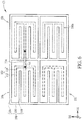
- FIG. 1 is a schematic diagram illustrating a top view of a MOM capacitor according to a first embodiment of the present invention.
- the MOM capacitor C1 includes a capacitor element 10 formed on a substrate (not shown), such as a substrate of a semiconductor chip or a die.
- the capacitor element 10 includes a first electrode 100 and a second electrode 102 not electrically connected to the first electrode 100.
- the first electrode 100 includes a plurality of first conductive strips 104, a plurality of second conductive strips 106, and a plurality of third conductive strips 108 electrically connected to each other.
- the first electrode 100 of this application further includes a plurality of segmental conductive strips 110.
- the second electrode 102 includes a plurality of fourth conductive strips 112 and a fifth conductive strip 114 electrically connected to each other.
- the first conductive strips 104, the third conductive strips 108, the segmental conductive strips 110, and the fourth conductive strips 112 are extended in a first direction D1 and formed of a first patterned conductive layer.
- the second conductive strips 106 and the fifth conductive strip 114 are extended in a second direction D2 and formed of a second patterned conductive layer, which is shown with different pattern shadings from the first patterned conductive layer for differentiation.
- the first direction D1 crosses the second direction D2. In this embodiment, the first direction D1 is perpendicular to the second direction D2, but not limited thereto.
- the second conductive strips 106 cross the first conductive strips 104, the third conductive strips 108, and the segmental conductive strips 110.
- Each of the first conductive strips 104 is electrically connected to the second conductive strips 106 through a plurality of first vias V1 respectively
- each of the third conductive strips 108 is electrically connected to the second conductive strips 106 through a plurality of second vias V2 respectively
- each of the segmental conductive strips 110 is electrically connected to the second conductive strip 106 through a fourth via V4. Therefore, the first conductive strips 104, the second conductive strips 106, the third conductive strips 108, and the segmental conductive strips 110 are electrically connected together to form the first electrode 100.
- the fifth conductive strip 114 crosses the fourth conductive strips 112, and each of the fourth conductive strips 112 is electrically connected to the fifth conductive strip 114 through a third via V3, such that the fourth conductive strips 112 and the fifth conductive strip 114 are electrically connected to each other and form the second electrode 102.
- the material of the conductive strips and vias of this embodiment may include metal, doped layer or other suitable conductive materials.
- the conductive strips and vias may be formed through conventional dual damascene processes and may include conductive materials, such as W, Al, AlCu, Cu, Ti, TiSi2, Co, CoSi2, Ni, NiSi, TiN, TiW, Ta, or TaN, but not limited thereto.
- the patterns of the projection of the first electrode 100 and the projection of the second electrode 102 in a vertical projection direction V is further detailed herein.
- the vertical projection direction V is perpendicular to both of the first direction D1 and the second direction D2 in this embodiment, and is also perpendicular to the surface of the substrate on which the MOM capacitor C1 disposed.
- the projection of each of the first conductive strips 104 is connected to the projections of two second conductive strips 106
- the projection of each of the second conductive strips 104 is connected to the projections of two first conductive strips 106.
- the projection of the first electrode 100 includes a closed pattern, like a frame, in the vertical projection direction V, which is made of two of the first conductive strips 104 and two of the second conductive strips in the capacitor element 10, and the projection of the second electrode 102 is surrounded by the closed pattern in the vertical projection direction V.
- the projection of each of the third conductive strips 108 is connected to the projection of one of the second conductive strips 106.
- the projection of each third conductive strip 108 is connected to the projections of two second conductive strips 106.
- the third conductive strips 108 are disposed between two adjoining first conductive strips 104, and each of the third conductive strips 108 is disposed between two adjoining segmental conductive strips 110 in the second direction D2.
- the third conductive strips 108 and the segmental conductive strips 110 are arranged alternately in the second direction D2.
- the projection of each of the fourth conductive strips 112 is connected to the projection of the fifth conductive strip 114, and the fourth conductive strips 112 and the third conductive strips 108 are disposed alternately in the second direction D2.
- each of the fourth conductive strips 112 is disposed between two of the segmental conductive strips 110 in the first direction D1, and the segmental conductive strips 110 and the fourth conductive strips 112 disposed therebetween are substantially aligned along the first direction D1.
- the segmental conductive strips 110 are isolated from the fourth conductive strips 112 by a dielectric material (not shown).
- the fifth conductive strip 114 is disposed between two of the second conductive strips 106 in the first direction D1. In addition, the projection of the fifth conductive strip 114 crosses the projections of third conductive strips 108, and the fifth conductive strip 114 is isolated from the third conductive strips 108 by the dielectric material (not shown).
- the first electrode 100 is a top electrode of the capacitor element 10, and the second electrode 102 is a bottom electrode of the capacitor element 10. Therefore, the first electrode 100 may be grounded or serves as an output terminal, and the second electrode 102 serves as an input terminal and may be electrically connected to an electronic device, such as a transistor, but not limited thereto.
- the capacitor element 10 is formed of two different patterned conductive layers, wherein the first patterned conductive layer includes the conductive strips that extend in the first direction D1, and the second patterned conductive layer includes the conductive strips that extend in the second direction D2. No curved lines or strips are formed in the first and second patterned conductive layers, and the strips in the different two patterned conductive layer of the same electrode are electrically connected through vias disposed between the patterned conductive layers. Therefore, the design of this embodiment can overcome the difficulty of perfectly forming the metal strips including curved patterns in the same metal layer in the advanced semiconductor manufacturing technologies.
- the design that closed pattern of the projection of the first electrode 100 surrounds the projection of the second electrode 102 means that the first electrode 100 (top electrode) substantially isolates the second electrode 102 from other electronic devices disposed nearby.
- the second electrode 102 is sandwiched in between two first conductive strips 104 so as to provide the isolation for the second electrode 102 in the second direction D2, and the second electrode 102 is sandwiched in between the two second conductive strips 106 so as to provide the isolation for the second electrode 102 in the first direction D1.
- the segmental conductive strips 110 formed of the same patterned conductive layer as the fourth conductive strips 112 are placed in the capacitor element 10 for effectively preventing the fourth conductive strips 112 from being interfered with other electronic devices around the capacitor element 10, especially in the first direction D1.
- the third conductive strips 108 and the fifth conductive strip 114 are formed of different patterned conductive layers, the third conductive strips 108 can cross the fifth conductive strip 114 without electrical connection. Therefore, the third conductive strips 108 is no longer required to be disconnected due to the existence of the fifth conductive strip 114, and the third conductive strips 108 can extend along the first direction D1 between two second conductive strips 106 and have a larger area. Thus, the capacity between the first electrode 100 and the second electrode 102 is improved. It is noteworthy that the stacking sequence is not specifically limited.
- the second patterned conductive layer may be formed above the first patterned conductive layer along the vertical projection direction V, but the inverse disposition may also be included in this embodiment.
- the amounts and relative lengths of the first conductive strips 104, the second conductive strips 106, the third conductive strips 108, the fourth conductive strips 112, and the fifth conductive strip 114 are limited to the example shown in FIG. 1 .
- the first electrode 100 may include four or more second conductive strips 106, and the second electrode 102 may also include two or more fifth conductive strips 114 arranged side by side in the first direction.
- the first conductive strips 104 and the third conductive strips 108 may have non-identical length.
- the MOM capacitor may include a plurality of capacitor elements 10 stacked in sequence along the vertical projection direction V.
- Each of the capacitor elements 10 is formed of two patterned conductive layers that are different from the patterned conductive layers of other the capacitor elements 10.
- the first electrodes 100 of the capacitor elements 10 may be electrically connected to each other through vias (not shown), and the second electrodes 102 of the capacitor elements 10 may be electrically connected to each other through other vias (not shown).
- the MOM capacitor in the variant embodiment includes a plurality of capacitor elements 10 formed of two patterned conductive layers shown in FIG 1 stacked in the vertical projection direction V in sequence, wherein the first electrodes 100 in all the capacitor elements 10 are electrically connected to each other through vias, and the second electrodes 102 in all the capacitor elements 10 are electrically connected to each other through vias.
- FIG. 2 is a schematic diagram illustrating a top view of a MOM capacitor according to a variant embodiment of the first embodiment of the present invention.
- the MOM capacitor C1' of this variant embodiment is mainly different from the first embodiment in the arrangement of the third conductive strips 108 and the numbers of some conductive strips.
- the third conductive strips 108 are shorter and does not cross the second conductive strips 106 at different sides of the fifth conductive strip 114 in the projection direction at the same time.
- the projection of each third conductive strip 108 only crosses the projection(s) of the second conductive strip(s) 106 at one side (or the same side) of the fifth conductive strips 114 in the vertical projection direction V.
- the first electrode 100 includes four second conductive strips 106, two of which are positioned at the left side of the fifth conductive strips 114 while the other two are positioned at the right side of the fifth conductive strips 114, and the second electrode 102 may also include two or more fifth conductive strips 114 arranged side by side in the first direction.
- the numbers of the third conductive strips 108, the fourth conductive strips 112, and the segmental conductive strips 110 of the MOM capacitor C1' in this variant embodiment are greater than those of the MOM capacitor C1 in the first embodiment.
- the first conductive strips 104 may have a longer length than the third conductive strips 108 which are sandwiched between the two first conductive strips 104.
- the amounts of the second conductive strips 106 and the fifth conductive strip 114 may be identical to the first embodiment, but each third conductive strip 108 does not cross the fifth conductive strip 114 and only crosses one second conductive strip 106 at one side of the fifth conductive strip 114 in the vertical projection direction V.
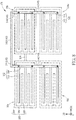
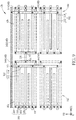
- FIG. 3 to FIG. 5 are figures illustrating a MOM capacitor according to a second embodiment of this application, wherein FIG. 3 is an equivalent circuit diagram of the MOM capacitor according to the second embodiment of the present invention, FIG. 4 is a schematic diagram illustrating a top view of the first and second patterned conductive layers of the MOM capacitor according to the second embodiment of the present invention, and FIG. 5 is a schematic diagram illustrating a layout of other patterned conductive layers of the MOM capacitor according to the second embodiment of the present invention.
- the MOM capacitor C2 of this application includes three capacitor elements 10a, 10b, 10c.
- the top electrodes of the capacitor elements 10a, 10b, 10c are electrically connected together as a common terminal X that is grounded or serves as an output terminal.
- the bottom electrodes of the capacitor elements 10a, 10b serve as input terminals Y
- the bottom electrode of the capacitor element 10c serves as another input terminal Z
- the input terminals Y, Z may be electrically connected to external electronic devices respectively, such as transistors, but not limited thereto.
- the top electrodes and the bottom electrodes of the capacitor elements 10a, 10b, 10c are represented with different line patterns or line segments respectively in order to reveal the electric connection relationship.
- the top electrodes (marked with "X") of the capacitor elements 10a, 10b, 10c are illustrated in solid lines
- the bottom electrodes (marked with "Y") of the capacitor elements 10a, 10b are illustrated in broken lines
- the capacitor element 10c (marked with "Z") is illustrated in broken lines with two dots between two segments.
- the MOM capacitor C2 of this embodiment includes a plurality of capacitor elements 10a, 10b, 10c and a dummy electrode 116a (shown in dotted lines) arranged in juxtaposition.
- the capacitor elements 10a, 10b, 10c and the capacitor element 10 in the first embodiment have similar top-view layouts, except that the adjoining capacitor elements 10a, 10b, 10c have a common first conductive strip 104C or a common second conductive strip 106C, and the projection or structure of the dummy electrode 116a is substantially the same as that of the second electrode 102 shown in FIG. 1 .
- the capacitor elements 10a, 10b, 10c are formed of two patterned conductive layers, wherein the first conductive strips 104, the third conductive strips 108, the segmental conductive strips 110, and the fourth conductive strips 112 are formed of a same first patterned conductive layer, and the second conductive strips 106 and the fifth conductive strips 114 are formed of a same second patterned conductive layer, as mentioned in the first embodiment.
- the projection of two of the first conductive strips 104 and the projection of two of the second conductive strips 106 in each of the capacitor elements 10a, 10b, 10c form the closed pattern
- the closed pattern of the capacitor element 10a is connected to the closed pattern of the capacitor element 10b in the first direction D1 and the closed pattern of the capacitor element 10c in the second direction D2.
- the projection of each first conductive strip 104 is connected to the projection of two or more second conductive strips 106 and the projection of each second conductive strip 106 is connected to the projection of two or more first conductive strips 106, so as to form the closed patterns.
- the capacitor element 10a and the capacitor element 10b are arranged in a line along the first direction D1, and the capacitor element 10a and the capacitor element 10b have a common second conductive strip 106C.
- the capacitor element 10a and the capacitor element 10c are arranged in a line along the second direction D2, and the capacitor element 10a and the capacitor element 10c have a common first conductive strip 104C. Accordingly, the closed patterns of the first electrodes 100 of the capacitor elements 10a, 10b, 10c are electrically connected together, as the common top electrode, which is the common terminal X shown in FIG. 3 and may be grounded or be an output terminal.
- the second electrodes 102 of the capacitor elements 10a and 10b and the second electrode 102 of the capacitor elements 10c are respectively serve as the bottom electrodes, the input terminals Y and Z in FIG. 3 , and are separated from each other by the first electrodes 100 in FIG. 4 .
- the MOM capacitor C2 further includes two optional dummy electrodes 116b adjacent to the capacitor elements 10a and 10c respectively.
- the constitution of the dummy electrodes 116b, and the dummy electrode 116a are similar, wherein the difference between the dummy electrode 116a and the dummy electrode 116b is that the projection of each dummy electrodes 116b has a pattern similar to the letter "E".
- the dummy electrodes 116a and 116b they are all surrounded by the first electrodes 100. Specifically, three first conductive strips 104 cross four second conductive strips 106, with electrical connection, to create six closed patterns of the first electrodes 100 in this embodiment.
- the closed patterns are arranged in a 2x3 matrix, wherein the capacitor element 10a and the capacitor element 10c are disposed in the first row and the second row of the second column respectively, the capacitor element 10b and the dummy electrode 116a are disposed in the first row and the second row of the third column respectively, and the dummy electrodes 116b are disposed within the closed patterns in the first row and the second row of the first column respectively.
- all of the first conductive strips 104, the second conductive strips 106, the third conductive strips 108, and the segmental conductive strips 110 are electrically connected together, and therefore the six closed patterns can also be regarded as one common first electrode 100.
- the second electrodes 102 of the capacitor elements 10a, 10b, 10c are respectively disposed in the corresponding closed patterns of the common first electrodes 100, each of which is shielded by the corresponding closed pattern of the common first electrode 100, and therefore the capacitor elements 10a, 10b, 10c are prevented from being influenced by each other or any other adjacent external electronic device.
- the common first electrode 100 has the segment conductive strips 110, it can provide good isolation effect for the second electrodes 102 of the capacitor elements 10a, 10b, 10c, as well as the dummy electrodes 116a and 116b.
- the constitution and materials of the first electrodes 100 and the second electrode 102 are the same as the first embodiment, and will not be redundantly described herein.
- the MOM capacitor C2 may include a plurality of capacitor elements 10a stacked in sequence along the vertical projection direction V, each of the capacitor elements 10a is formed of two patterned conductive layers different from any patterned conductive layers of any other one of the capacitor elements 10a, the first electrodes 100 of the capacitor elements 10a are electrically connected to each other through vias (not shown), and the second electrodes 102 of the capacitor elements 10a are electrically connected to each other through vias (not shown) .
- the method of integrating a plurality of capacitor elements 10b and the method of integrating a plurality of capacitor elements 10c may be the same as that of the capacitor elements 10a, thus detailed description will not be redundantly repeated.
- FIG. 5 illustrates other four patterned conductive layers of the MOM capacitor C2, which may be stacked above the first and second pattern conductive layers shown in FIG. 4 along the vertical projection direction V.
- the MOM capacitor C2 in the vertical projection direction V, includes a plurality of first shielding strips 118 disposed corresponding to the first conductive strips 104, a plurality of second shielding strips 120 disposed corresponding to the second conductive strips 106, two first auxiliary strips 122 disposed corresponding to the fifth conductive strips 114 of the capacitor elements 10a, 10b respectively, a second auxiliary strip 124 disposed corresponding to the fifth conductive strip 114 of the capacitor element 10c, a dummy strip 126a and a dummy strip 126bdisposed corresponding to the dummy electrode 116a, and two of the dummy strips 126c disposed corresponding to the dummy electrodes 116b.
- the MOM capacitor C2 further includes a first bridge line 128 crossing two first auxiliary strips 122 and the dummy strip 126c in the vertical projection direction V, and a second bridge line 130 crossing the second auxiliary strip 124 and the dummy strip 126c in the vertical projection direction V.
- the first shielding strips 118 extend in the first direction D1 and are formed of a third patterned conductive layer
- the second shielding strips 120, the first auxiliary strips 122, the second auxiliary strip 124, and the dummy strips 126a, 126c all extend in the second direction D2, and they are all formed of a same fourth patterned conductive layer.
- first bridge line 128, the second bridge line 130, and the dummy strip 126b extend in the first direction D1, and they are formed of a same fifth patterned conductive layer.
- the fourth patterned conductive layer is disposed between the third patterned conductive layer and the fifth patterned conductive layer, and the fifth patterned conductive layer is disposed above the third patterned conductive layer in the vertical projection direction V.
- a plurality of third shielding strips 132 may be disposed corresponding to the dummy electrodes 116b and extend in the first direction D1.
- the third shielding strips 132 are formed of a sixth patterned conductive layer, and the sixth patterned conductive layer is disposed between the fifth patterned conductive layer and the fourth patterned conductive layer in the vertical projection direction V.
- each first auxiliary strip 122 is electrically connected to the corresponding second electrode 102 of the capacitor element 10a or 10b through a via (not shown) respectively, and the first bridge line 128 is electrically connected to both of the first auxiliary strips 122 through a plurality of vias Va respectively. Therefore, the second electrodes 102, i.e. the bottom electrodes, of the capacitor elements 10a, 10b can both be electrically connected to the first bridge line 128.
- the second auxiliary strip 124 may be electrically connected to the corresponding second electrode 102 of the capacitor elements 10c through a via (not shown), and the second bridge line 130 is electrically connected to the second auxiliary strip 124 through a via Vb. Therefore, the second electrode 102, i.e.
- the bottom electrode, of the capacitor element 10c can be electrically connected to the second bridge line 130.
- the first bridge line 128 and the second bridge line 130 may further extend leftward to be electrically connected to electronic devices, such as transistors, but not limited thereto, such that they serve as input terminals for inputting signals or voltages to the bottom electrodes of the capacitor elements 10a, 10b, 10c respectively.
- the first shielding strips 118 and the second shielding strips 120 are electrically connected together through the vias Vc.
- the projection of the first shielding strips 118 and the second shielding strips 120 also form a plurality of closed patterns that surround the first auxiliary strips 122, the second auxiliary strip 122, the dummy strips 126a, 126b, 126c, thus they can further prevent the first electrodes 100 and the second electrodes 102 of the first patterned conductive layer and the second patterned conductive layer from being influenced by the other electronic components disposed at the higher levels of the patterned conductive layer.
- the disposition of the third shielding strips 132 formed of the sixth patterned conductive layer prevents the coupling between the dummy strip 126c and the first bridge line 128, and the coupling between the dummy strip 126c and the second bridge line 130.
- FIG. 6 is a schematic diagram illustrating a top view of a MOM capacitor according to a third embodiment of the present invention.
- the MOM capacitor C3 of this embodiment includes three capacitor elements 10a, 10b, 10c, whose equivalent circuit is the same as the second embodiment shown in FIG. 3 . Therefore, the second electrodes 102 of the capacitor elements 10a and 10b are electrically connected together, but not electrically connected to the second electrode 102 of the capacitor element 10c, and the first electrodes 100 of all the three capacitor elements 10a, 10b, 10c are electrically connected together.
- the MOM capacitor C3 has only one dummy electrode 116a, without the dummy electrodes 116b shown in FIG.
- the capacitor elements 10a, 10b, 10c and the dummy electrode 116a are formed of the same patterned conductive layer.
- Three first conductive strips 104 cross three second conductive strips 106 to create four closed patterns and form the common first electrode 100, i.e. the common top electrode, of the capacitor elements 10a, 10b, 10c.
- the capacitor element 10a and the capacitor element 10c are disposed in the first row and the second row of the first column respectively, and the capacitor element 10b and the dummy electrode 116a are disposed in the first row and the second row of the second column respectively.
- the second electrodes 102 of three capacitor elements 10a, 10b, 10c and the dummy electrode 116a are surrounded by the first electrodes 100 to avoid interference with external electronic devices. It is noteworthy that the projection patterns of the second electrodes 102 and the first electrodes 100 of the capacitor elements 10a, 10b, 10c in this embodiment are different from that of the second embodiment.
- Each of the third conductive strips 108 is connected to only one of the second conductive strips 106, and the third conductive strips 108 do not cross the fifth conductive strip 114 in each of the closed patterns.
- each of the fourth conductive strips 112 is connected to the fifth conductive strip 114 of the same second electrode 102, so as to form a pattern similar to the digital number of "3".
- the fourth conductive strips 112 and the third conductive strips 108 are interdigitated in the second direction D2 and separated from one another.
- the dummy electrode 116a has the same pattern as the second electrodes 102 of the capacitor elements 10a, 10b, 10c, and therefore the strips extending along the first direction D1 of the dummy electrode 116a and the third conductive strips 108 of the first electrode 100 in the lower right closed pattern are also interdigitated.
- first electrodes 100 and the second electrodes 102 are formed of the same patterned conductive layer, such as a first patterned conductive layer
- a bridge line 134 made of another patterned conductive layer, such as a second patterned conductive layer is used for electrically connecting the second electrodes 102 of the capacitor element 10a and the capacitor element 10b.
- two opposite ends of the bridge line 134 are electrically connected to the fifth conductive strip 114 of the capacitor element 10a and the fourth conductive strips 112 of the capacitor element 10b through vias Vd respectively, but not limited thereto.
- first electrodes 100 are grounded or serve as output terminals, and the second electrodes 102 serve as input terminals, thus the second electrodes 102 or the bridge line 134 may be further electrically connected to another conductive line (not shown) for inputting signals or voltages.
- the second electrodes 102 since each of the second electrodes 102 is disposed in the corresponding closed pattern of the first electrode 100 made of the same patterned conductive layer, the second electrodes 102 are prevented from being influenced by each other or by other adjacent external electronic devices, and the design of the segmental conductive strips 110 mentioned in the first or second embodiments is not adopted in this embodiment.
- FIG. 7 is a schematic diagram illustrating a top view of a MOM capacitor according to a fourth embodiment of the present invention.
- the difference between the MOM capacitor C4 of this embodiment and the MOM capacitor C3 of the third embodiment is that the first conductive strips 104, the third conductive strips 108, and the fourth conductive strips 112 are formed of the same patterned conductive layer, such as a first patterned conductive layer, and the second conductive strips 106 and the fifth conductive strips 114 are formed of another patterned conductive layer, such as a second patterned conductive layer.
- the MOM capacitor C4 includes a bridge line 136 extending in the first direction D1 and directly connected to one of the fourth conductive strips 112 of the capacitor elements 10a and one of the fourth conductive strips 112 of the capacitor elements 10b.
- the bridge line 136 is formed of the same patterned conductive layer as the fourth conductive strips 112, such as the first patterned conductive layer.
- the bridge line 136 and two connected fourth conductive strips 112 are formed of the same conductive line extending from the capacitor element 10a to the capacitor element 10b in the first direction D1.
- the bridge line 136 may be formed of another patterned conductive layer that is different from the first patterned conductive layer and the second patterned conductive layer in a variant embodiment.
- segmental conductive strips 110 are formed of the same patterned conductive layer as the fourth conductive strips 112, such as the first patterned conductive layer.
- the segmental conductive strips 110 are part of the first electrodes 100, and the first electrodes 100 may be grounded for example. Therefore, the fourth conductive strips 112 of the second electrodes 102 of the capacitor elements 10a, 10b, 10c can be effectively isolated from other adjacent electronic devices in the first direction D1.
- the method of electrically connecting the second conductive strips 106 to the first conductive strips 104, the third conductive strips 108, and the segmental conductive strips 110, and the method of electrically connecting the fourth conductive strips 112 to the fifth conductive strips 114 are the same as the first embodiment.
- the equivalent circuit diagram in FIG. 3 may also be applied to the MOM capacitor C4 in this embodiment.
- FIG. 8 is a schematic diagram illustrating a top view of a MOM capacitor according to a fifth embodiment of the present invention.
- the equivalent circuit of the MOM capacitor C5 of this embodiment is the same as that of the second embodiment shown in FIG. 3 .
- the difference between the MOM capacitor C5 of this embodiment and the MOM capacitor C3 of the third embodiment is that the first electrodes 100 of the capacitor elements 10a, 10b, 10c are separated from one another, and the first electrodes 100 and the second electrodes 102 respectively serve as the bottom electrodes and the top electrodes of the capacitor elements 10a, 10b, 10c.
- the projection of two first conductive strips 104 and two second conductive strips 106 of the first electrode 100 in each of the capacitor elements 10a, 10b, 10c form a closed pattern, and the closed pattern of one of the capacitor elements 10a, 10b, 10c is separated from the closed pattern of any other one of the capacitor elements 10a, 10b, 10c in the vertical projection direction V.
- a connection line 138 is used for electrically connecting the first electrode 100 of the capacitor element 10a and the first electrode 100 of the capacitor element 10b, so as to electrically connect the bottom electrodes of the capacitor elements 10a and 10b for providing a common input terminal Y shown in FIG. 3 , while the first electrode 100 of the capacitor element 10c serves as a separate input terminal z.
- connection line 138 of this embodiment is formed of the same patterned conductive layer as the second conductive trips 106, but not limited thereto.
- one end of the connection line 138 is directly connected to the right second conductive strip 106 of the capacitor element 10a that is adjoining to the capacitor element 10b, and another end of the connection line 138 is directly connected to the left second conductive strip 106 of the capacitor element 10b that is adjoining to the capacitor element 10a.
- the MOM capacitor C5 further includes a dummy electrode 116c arranged in juxtaposition with the capacitor elements 10a, 10b, 10c.
- a projection of the dummy electrode 116c is substantially the same as the projection of the first electrodes 100, and therefore the dummy electrode 116c also has a closed pattern that surrounds a second electrode 102.
- the first conductive strips 104, the second conductive strips 106, the third conductive strips 108, and the fourth conductive strips 112 of the capacitor elements 10a, 10b, 10c, the dummy electrode 116c, and the connection line 138 are formed of the same patterned conductive layer, such as a first patterned conductive layer.
- the fifth conductive strips 114 and a bridge line 140 are formed of another patterned conductive layer, such as a second patterned conductive layer.
- the bridge line 140 is directly connected to the fifth conductive strips 114 of the capacitor elements 10a, 10b, 10c and the fifth conductive strip 114 surrounded by the dummy electrode 116c in order to electrically connect all the second electrodes 102 to form a common top electrode serving as a common output terminal X shown in FIG. 3 or being grounded.
- the bridge line 140 includes a first bridge strip 142 and a plurality of second bridge strips 144.
- the first bridge strip 142 extends in the first direction D1 and is disposed outside the closed patterns.
- the second bridge strips 144 extend in the second direction D2 and are disposed between the first bridge strip 142 and the fifth conductive strips 114 of the capacitor element10a and the capacitor element 10b respectively.
- the second bridge strips 144 are also disposed between the fifth conductive strips 114 of the capacitor element 10a and the capacitor element 10c and disposed between the fifth conductive strip 114 of the capacitor element10b and the fifth conductive strip 114 surrounded by the dummy electrode 116c.
- the first bridge strip 142 and the fifth conductive strips 114 are all connected together through the second bridge strips 144.
- FIG. 9 is a schematic diagram illustrating a top view of a MOM capacitor according to a sixth embodiment of the present invention.
- the difference between the MOM capacitor C6 of this embodiment and the fifth embodiment is that the first conductive strips 104, the third conductive strips 108, and the fourth conductive strips 112 are formed of the same patterned conductive layer, such as a first patterned conductive layer, while the second conductive strips 106, the fifth conductive strips 114, and the second bridge strips 144 are formed of another patterned conductive layer, such as a second patterned conductive layer.
- the first bridge strip 142 is formed of still another patterned conductive layer, such as a third patterned conductive layer.
- Each of the second bridge strips 144 is directly connected to one of the fifth conductive strips 114, and at least one of the second bridge strips 144 is electrically connected to the first bridge strip 142 through a fifth via V5.
- the first bridge strip 142 is formed of the same patterned conductive layer as the first conductive strip 104, and is also electrically connected to the second bridge strips 144 through the vias V5.
- the structure of the dummy electrode 116c is similar to the first electrodes 100 of the capacitor elements 10a, 10b, 10c.
- a portion of the dummy electrode 116c that extends in the first direction D1 is formed of the same patterned conductive layer as the first conductive strips 104, the third conductive strips 108, and the fourth conductive strips 112.
- Another portion of the dummy electrode 116c that extends in the second direction D2 is formed of the same patterned conductive layer as the second conductive strips 106 and the fifth conductive strips 114. These two portions of the dummy electrode 116c are electrically connected through vias. Moreover, the connection line 138 is electrically connected to the second conductive strip 106 of the capacitor element 10a adjoining to the capacitor element 10b through a via Ve, and is electrically connected to the second conductive strip 106 of the capacitor element 10b adjoining to the capacitor element 10a through a via Vf. It is noteworthy that the segmental conductive strips 110 mentioned in the first and fourth embodiments are also placed in each first electrode 100 of the capacitor elements 10a, 10b, 10c.
- Each segmental conductive strip 110 is formed of the same patterned conductive layer as the fourth conductive strips 112 and is electrically connected to one second conductive strip 106 through a via V4. The placement of the segmental conductive strips 110 provides good isolation performance for the adjoining fourth conductive strips 112 in the first direction D1 from other adjacent external electronic devices.
- FIG. 10 to FIG. 12 are schematic diagrams illustrating top views of a MOM capacitor according to a seventh embodiment of the present invention, wherein FIG. 10 shows the top view of a first patterned conductive layer of the seventh embodiment, FIG. 11 shows the top view of a second patterned conductive layer and a third patterned conductive layer of the seventh embodiment, and FIG. 12 shows the top view of a fourth patterned conductive layer and bridge lines of a fifth patterned conductive layer of the seventh embodiment.
- the equivalent circuit of the MOM capacitor C7 can be represented as the circuit shown in FIG. 3 .
- the difference between this embodiment and the fifth embodiment is that the MOM capacitor C7 of this embodiment includes five patterned conductive layers integrated in the vertical projection direction V.
- each of the other patterned conductive layers forms three capacitor elements 10a, 10b, 10c.
- the MOM capacitor C7 includes a plurality of capacitor elements, wherein some of them are stacked layer by layer in the vertical projection direction V, and some of them are arranged in juxtaposition in the same layer.
- the projection of two first conductive strips 104 and two second conductive strips 106 in each of the capacitor elements 10a, 10b, 10c form a closed pattern, and each closed pattern of one of the capacitor elements 10a, 10b, 10c is separated from another one of the capacitor elements 10a, 10b, 10c in the vertical projection direction V.
- the projection of the dummy electrode 116c is substantially the same as the projection of the first electrodes 100, and therefore the dummy electrode 116c also has a closed pattern, which surrounds a second electrode 102, as mentioned in the sixth embodiment.
- the capacitor elements 10a, 10b, 10c and the dummy electrode 116c are formed of a first patterned conductive layer.
- the first electrode 100 of the capacitor element 10a is electrically connected to the first electrode 100 of another capacitor element 10a in a second patterned conductive layer shown in FIG. 11 through at least one via Vg.
- the second electrode 102 of the capacitor element 10a is electrically connected to the second electrode 102 of another capacitor element 10a in the second patterned conductive layer shown in FIG. 11 through at least one via Vh.
- the above mentioned connecting method is also applied to the capacitor elements 10b and 10c and the second electrode 102 surrounded by the dummy electrode 116c.
- FIG. 11 shows the top views of the second patterned conductive layer and third patterned conductive layer of the MOM capacitor C7, wherein the second and the third patterned conductive layers have the same top views.
- the difference between the top view of the second patterned conductive layer shown in FIG. 11 and the top view of the first patterned conductive layer shown in FIG. 10 is that the second patterned conductive layer further includes a plurality of first connection lines 146 and a second connection line 148.
- the first connection lines 146 and the second connection line 148 both extend in the first direction D1, wherein each second conductive strips 106 of the capacitor elements 10a, 10b connects to one first connection lines 146, and the second connection line 148 connects to the second conductive strips 106 of the capacitor element 10c that is not positioned adjoining to the dummy electrode 116c.
- the first connection line 146 positioned between the capacitor element 10a and the capacitor element 10b is used for electrically connecting the first electrodes 100 of the capacitor elements 10a and 10b, and the other first connection lines 146 can be used for electrically connecting other electronic device to the capacitor element 10a and the capacitor element 10b.
- the second connection line 148 can be used for electrically connecting other electronic device to the capacitor element 10c, but not limited thereto.
- the first connection lines 146 and the second connection line 148 can deliver signals or voltages to the corresponding first electrodes 100 of the capacitor elements 10a, 10b, 10c, such that the first electrodes 100 serve as the bottom electrodes or input terminals of the capacitor elements 10a, 10b, 10c.
- the third patterned conductive layer of the MOM capacitor C7 of this embodiment also includes the first and second connection lines 146, 148.
- the first connection lines 146 or the second connection line 148 may only be arranged in one of the second patterned conductive layer and the third conductive patterned layer.
- the first electrode 100 of the capacitor element 10a is electrically connected to the first electrode 100 of another capacitor element 10a in the third patterned conductive layer through at least one via Vi.
- the second electrode 102 of the capacitor element 10a is electrically connected to the second electrode 102 of another capacitor element 10a in the third patterned conductive layer through at least one via Vj.
- the above mentioned connecting method is also applied to the capacitor elements 10b and 10c and the second electrode 102 surrounded by the dummy electrode 116c.
- the capacitor elements 10a, 10b, 10c in the third patterned conductive layer can be electrically connected to the corresponding capacitor elements 10a, 10b, 10c in the fourth patterned conductive layer through corresponding vias by the same way mentioned-above.
- FIG. 12 illustrates the fourth patterned conductive layer and the fifth patterned conductive layer of the MOM capacitor C7, wherein the fifth patterned conductive layer is shown by a dotted pattern shading, while the fourth patterned conductive layer is shown without shading.
- the pattern of the fourth patterned conductive layer is similar to the first patterned conductive layer shown in FIG. 10 , excepting that a first connection line 150 included by the fourth patterned conductive layer is selectively disposed between the capacitor element 10a and the capacitor element 10b, which directly connects to the adjoining second conductive strips 106 of the capacitor element 10a and the capacitor element 10b.
- the fifth patterned conductive layer it includes two bridge lines 152 that extend in the second direction D.
- One of the bridge lines 152 is electrically connected to the second electrode 102 of the capacitor element 10a and the second electrode 102 of the capacitor element 10c through a plurality of vias Vk, and another bridge line 152 is electrically connected to the second electrode 102 of the capacitor element 10b and the second electrode 102 surrounded by the dummy electrode 116c through a plurality of vias V1.
- the bridge line 152 may be further electrically connected to each other for electrically connecting all the second electrodes 102 of the capacitor elements 10a, 10b, 10c in the first, second, third, and fourth patterned conductive layers, so as to form a common second electrode.
- the first electrode 100 is a bottom electrode, which may serve as an input terminal
- the second electrode 102 is a top electrode that may serve as an output terminal or be grounded. Therefore, the bridge lines 152 may be grounded or serve as an output terminal to be further electrically connected to an external electronic device.
- the patterns of each of the first, second, third, and fourth conductive layer can further be separate to two conductive layers, wherein one has the patterns of strips extending in the first direction D1 and another one has the patterns of strips extending in the second direction D2, as the design theory mentioned in the first, second, and fourth embodiments.
- segmental strips may further be adopted to provide more effective isolation for the second electrodes.
- each capacitor element includes the first electrode having a closed pattern in the vertical projection direction, and the projection of the second electrode is surrounded by the closed pattern of the projection of the first electrode.
- each of the capacitor elements can be prevented from being influenced by each other when the capacitor elements are arranged in an array, and this design also avoids interference between these capacitor and any other outer electronic devices, thus the linearity of the MOM capacitor can be improved.
- each capacitor element can be formed of two different patterned conductive layers, wherein the first patterned conductive layer includes the conductive strips that extend in one direction, and the second patterned conductive layer includes the conductive strips that extend in another direction.
- adopting this design can overcome the difficulty of accurately forming the metal strips including curved patterns in the same metal layer in the advanced semiconductor manufacturing technologies with high integration density. Furthermore, when the conductive strips in one of the patterned conductive layer all extend in one direction, the projection of the segmental conductive strips of the first electrode and the projection of the fourth conductive strips of the second electrode are aligned in the extending direction, such that placing the segmental conductive strips in the capacitor element can effectively prevent the second electrode of the capacitor element from being interfered with other capacitor elements around the capacitor element in the extending direction.
Landscapes
- Engineering & Computer Science (AREA)
- Power Engineering (AREA)
- Microelectronics & Electronic Packaging (AREA)
- Manufacturing & Machinery (AREA)
- Semiconductor Integrated Circuits (AREA)
Abstract
Description
- The present invention is related to a metal-oxide-metal (MOM) capacitor which can overcome the difficulty of accurately forming the metal strips including curved patterns, or can provide good isolation for the capacitor element of the MOM capacitor according to the pre-characterizing clause of
claim 1. - Since the semiconductor industry continues to improve the integration density of electronic components by continual reductions in minimum feature size, it is now difficult to form the metal strips including curved patterns accurately. Therefore, forming a metal strip or a metal frame with a certain curved pattern for isolating another metal strip in each capacitor element in the same metal layer becomes much difficult. Hence, the capacitor elements arranged in an array will interfere with each other and the linearity of the capacitors will be degraded.
- This in mind, the present invention aims at providing a metal-oxide-metal (MOM) capacitor which can overcome the difficulty of accurately forming the metal strips including curved patterns, or can provide good isolation for the capacitor element of the MOM capacitor.
- This is achieved by a MOM capacitor according to
claim 1. The dependent claims pertain to corresponding further developments and improvements. - As will be seen more clearly from the detailed description following below, the claimed MOM capacitor comprises a capacitor element, wherein the capacitor element includes a first electrode and a second electrode. A projection of the first electrode includes a closed pattern in the vertical projection direction, and a projection of the second electrode is surrounded by the closed pattern of the projection of the first electrode in the vertical projection direction.
- In the MOM capacitor of the present invention, the projection of the second electrode is surrounded by the closed pattern of the projection of the first electrode. Accordingly, each of the capacitor elements can be prevented from being influenced by any other electronic devices, and the linearity of the MOM capacitor can be improved. In addition, the present invention provides a design to form a capacitor element with two patterned conductive layers, wherein each of the patterned conductive layers includes the conductive strips that only extend in one direction. Therefore, the difficulty of precisely forming the metal strips including curved patterns in the same metal layer in the prior art can be resolved.
- In the following, the invention is further illustrated by way of example, taking reference to the accompanying drawings. Thereof
-
FIG. 1 is a schematic diagram illustrating a top view of a MOM capacitor according to a first embodiment of the present invention, -
FIG. 2 is a schematic diagram illustrating a top view of a MOM capacitor according to a variant embodiment of the first embodiment of the present invention, -
FIG. 3 is an equivalent circuit diagram of a MOM capacitor according to a second embodiment of the present invention, -
FIG. 4 is a schematic diagram illustrating a top view of the first and second patterned conductive layers of the MOM capacitor according to the second embodiment of the present invention, -
FIG. 5 is a schematic diagram illustrating a layout of other patterned conductive layers of the MOM capacitor according to a second embodiment of the present invention, -
FIG. 6 is a schematic diagram illustrating a top view of a MOM capacitor according to a third embodiment of the present invention, -
FIG. 7 is a schematic diagram illustrating a top view of a MOM capacitor according to a fourth embodiment of the present invention, -
FIG. 8 is a schematic diagram illustrating a top view of a MOM capacitor according to a fifth embodiment of the present invention, -
FIG. 9 is a schematic diagram illustrating a top view of a MOM capacitor according to a sixth embodiment of the present invention, -
FIG. 10 is a schematic diagram illustrating a top view of a first patterned conductive layer of a MOM capacitor according to a seventh embodiment of the present invention, -
FIG. 11 is a schematic diagram illustrating a top view of a second patterned conductive layer and a third patterned conductive layer of the MOM capacitor according to the seventh embodiment of the present invention, and -
FIG. 12 is a schematic diagram illustrating a top view of a fourth patterned conductive layer and bridge lines of a fifth patterned conductive layer of the MOM capacitor according to the seventh embodiment of the present invention. - To provide a better understanding of the present invention, preferred embodiments will be detailed as follows. The preferred embodiments of the present invention are illustrated in the accompanying drawings with numbered elements to elaborate the contents and effects to be achieved.
- In the embodiments of the present invention, the term "vertical projection direction" is defined as a direction perpendicular to a plane, such as the surface of the semiconductor chip or the die substrate. The term "projection" of the electrodes or the conductive strips refers to patterns of the electrodes or the conductive strips that are projected in the vertical projection direction to the plane, such as the surface of the semiconductor chip or the die substrate.
- For clearly expressing the main features of the embodiments of the present invention, the dielectric material in the metal-oxide-metal (MOM) capacitor is omitted from the drawings of the embodiments. For those ordinary skills in the art of semiconductor manufacturing technologies, it should be understood that the dielectric material is formed between the electrodes or the conductive strips in the same patterned conductive layer for the purpose of isolation, and the dielectric material is also formed between different patterned conductive layers.
- Referring to
FIG. 1, FIG. 1 is a schematic diagram illustrating a top view of a MOM capacitor according to a first embodiment of the present invention. As shown inFIG. 1 , according to the first embodiment, the MOM capacitor C1 includes acapacitor element 10 formed on a substrate (not shown), such as a substrate of a semiconductor chip or a die. Thecapacitor element 10 includes afirst electrode 100 and asecond electrode 102 not electrically connected to thefirst electrode 100. Thefirst electrode 100 includes a plurality of firstconductive strips 104, a plurality of secondconductive strips 106, and a plurality of thirdconductive strips 108 electrically connected to each other. Thefirst electrode 100 of this application further includes a plurality of segmentalconductive strips 110. Thesecond electrode 102 includes a plurality of fourthconductive strips 112 and a fifthconductive strip 114 electrically connected to each other. In this embodiment, the firstconductive strips 104, the thirdconductive strips 108, the segmentalconductive strips 110, and the fourthconductive strips 112 are extended in a first direction D1 and formed of a first patterned conductive layer. The secondconductive strips 106 and the fifthconductive strip 114 are extended in a second direction D2 and formed of a second patterned conductive layer, which is shown with different pattern shadings from the first patterned conductive layer for differentiation. The first direction D1 crosses the second direction D2. In this embodiment, the first direction D1 is perpendicular to the second direction D2, but not limited thereto. The secondconductive strips 106 cross the firstconductive strips 104, the thirdconductive strips 108, and the segmentalconductive strips 110. Each of the firstconductive strips 104 is electrically connected to the secondconductive strips 106 through a plurality of first vias V1 respectively, each of the thirdconductive strips 108 is electrically connected to the secondconductive strips 106 through a plurality of second vias V2 respectively, and each of the segmentalconductive strips 110 is electrically connected to the secondconductive strip 106 through a fourth via V4. Therefore, the firstconductive strips 104, the secondconductive strips 106, the thirdconductive strips 108, and the segmentalconductive strips 110 are electrically connected together to form thefirst electrode 100. In another aspect, the fifthconductive strip 114 crosses the fourthconductive strips 112, and each of the fourthconductive strips 112 is electrically connected to the fifthconductive strip 114 through a third via V3, such that the fourthconductive strips 112 and the fifthconductive strip 114 are electrically connected to each other and form thesecond electrode 102. The material of the conductive strips and vias of this embodiment may include metal, doped layer or other suitable conductive materials. For example, the conductive strips and vias may be formed through conventional dual damascene processes and may include conductive materials, such as W, Al, AlCu, Cu, Ti, TiSi2, Co, CoSi2, Ni, NiSi, TiN, TiW, Ta, or TaN, but not limited thereto. - The patterns of the projection of the
first electrode 100 and the projection of thesecond electrode 102 in a vertical projection direction V is further detailed herein. The vertical projection direction V is perpendicular to both of the first direction D1 and the second direction D2 in this embodiment, and is also perpendicular to the surface of the substrate on which the MOM capacitor C1 disposed. In the vertical projection direction V, the projection of each of the firstconductive strips 104 is connected to the projections of two secondconductive strips 106, and the projection of each of the secondconductive strips 104 is connected to the projections of two firstconductive strips 106. Therefore, the projection of thefirst electrode 100 includes a closed pattern, like a frame, in the vertical projection direction V, which is made of two of the firstconductive strips 104 and two of the second conductive strips in thecapacitor element 10, and the projection of thesecond electrode 102 is surrounded by the closed pattern in the vertical projection direction V. In addition, the projection of each of the thirdconductive strips 108 is connected to the projection of one of the secondconductive strips 106. In this embodiment, the projection of each thirdconductive strip 108 is connected to the projections of two secondconductive strips 106. The thirdconductive strips 108 are disposed between two adjoining firstconductive strips 104, and each of the thirdconductive strips 108 is disposed between two adjoining segmentalconductive strips 110 in the second direction D2. In other words, the thirdconductive strips 108 and the segmentalconductive strips 110 are arranged alternately in the second direction D2. The projection of each of the fourthconductive strips 112 is connected to the projection of the fifthconductive strip 114, and the fourthconductive strips 112 and the thirdconductive strips 108 are disposed alternately in the second direction D2. Furthermore, each of the fourthconductive strips 112 is disposed between two of the segmentalconductive strips 110 in the first direction D1, and the segmentalconductive strips 110 and the fourthconductive strips 112 disposed therebetween are substantially aligned along the first direction D1. However, it should be noted that the segmentalconductive strips 110 are isolated from the fourthconductive strips 112 by a dielectric material (not shown). The fifthconductive strip 114 is disposed between two of the secondconductive strips 106 in the first direction D1. In addition, the projection of the fifthconductive strip 114 crosses the projections of thirdconductive strips 108, and the fifthconductive strip 114 is isolated from the thirdconductive strips 108 by the dielectric material (not shown). - In this embodiment, the
first electrode 100 is a top electrode of thecapacitor element 10, and thesecond electrode 102 is a bottom electrode of thecapacitor element 10. Therefore, thefirst electrode 100 may be grounded or serves as an output terminal, and thesecond electrode 102 serves as an input terminal and may be electrically connected to an electronic device, such as a transistor, but not limited thereto. - According to this embodiment, the
capacitor element 10 is formed of two different patterned conductive layers, wherein the first patterned conductive layer includes the conductive strips that extend in the first direction D1, and the second patterned conductive layer includes the conductive strips that extend in the second direction D2. No curved lines or strips are formed in the first and second patterned conductive layers, and the strips in the different two patterned conductive layer of the same electrode are electrically connected through vias disposed between the patterned conductive layers. Therefore, the design of this embodiment can overcome the difficulty of perfectly forming the metal strips including curved patterns in the same metal layer in the advanced semiconductor manufacturing technologies. For example, since the patterns of the firstconductive strips 104, the thirdconductive strips 108, and the secondconductive strips 112 and the segmentalconductive strips 110 are straight lines along the first direction D1, it is easy to form these patterns through a lithography process even if in a dense pattern application. In addition, the design that closed pattern of the projection of thefirst electrode 100 surrounds the projection of thesecond electrode 102 means that the first electrode 100 (top electrode) substantially isolates thesecond electrode 102 from other electronic devices disposed nearby. For example, thesecond electrode 102 is sandwiched in between two firstconductive strips 104 so as to provide the isolation for thesecond electrode 102 in the second direction D2, and thesecond electrode 102 is sandwiched in between the two secondconductive strips 106 so as to provide the isolation for thesecond electrode 102 in the first direction D1. Furthermore, in order to provide a complete isolation to the fourthconductive strips 112 of the second electrode 102 (bottom electrode) in the first direction D1, the segmentalconductive strips 110 formed of the same patterned conductive layer as the fourthconductive strips 112 are placed in thecapacitor element 10 for effectively preventing the fourthconductive strips 112 from being interfered with other electronic devices around thecapacitor element 10, especially in the first direction D1. Furthermore, since the thirdconductive strips 108 and the fifthconductive strip 114 are formed of different patterned conductive layers, the thirdconductive strips 108 can cross the fifthconductive strip 114 without electrical connection. Therefore, the thirdconductive strips 108 is no longer required to be disconnected due to the existence of the fifthconductive strip 114, and the thirdconductive strips 108 can extend along the first direction D1 between two secondconductive strips 106 and have a larger area. Thus, the capacity between thefirst electrode 100 and thesecond electrode 102 is improved. It is noteworthy that the stacking sequence is not specifically limited. For example, the second patterned conductive layer may be formed above the first patterned conductive layer along the vertical projection direction V, but the inverse disposition may also be included in this embodiment. - It should be noted that the amounts and relative lengths of the first
conductive strips 104, the secondconductive strips 106, the thirdconductive strips 108, the fourthconductive strips 112, and the fifthconductive strip 114 are limited to the example shown inFIG. 1 . For example, in one variant embodiment, thefirst electrode 100 may include four or more secondconductive strips 106, and thesecond electrode 102 may also include two or more fifthconductive strips 114 arranged side by side in the first direction. In addition, the firstconductive strips 104 and the thirdconductive strips 108 may have non-identical length. - In another variant embodiment, the MOM capacitor may include a plurality of
capacitor elements 10 stacked in sequence along the vertical projection direction V. Each of thecapacitor elements 10 is formed of two patterned conductive layers that are different from the patterned conductive layers of other thecapacitor elements 10. In addition, thefirst electrodes 100 of thecapacitor elements 10 may be electrically connected to each other through vias (not shown), and thesecond electrodes 102 of thecapacitor elements 10 may be electrically connected to each other through other vias (not shown). In short, the MOM capacitor in the variant embodiment includes a plurality ofcapacitor elements 10 formed of two patterned conductive layers shown inFIG 1 stacked in the vertical projection direction V in sequence, wherein thefirst electrodes 100 in all thecapacitor elements 10 are electrically connected to each other through vias, and thesecond electrodes 102 in all thecapacitor elements 10 are electrically connected to each other through vias. - Referring to
FIG. 2, FIG. 2 is a schematic diagram illustrating a top view of a MOM capacitor according to a variant embodiment of the first embodiment of the present invention. The MOM capacitor C1' of this variant embodiment is mainly different from the first embodiment in the arrangement of the thirdconductive strips 108 and the numbers of some conductive strips. In this variant embodiment, the thirdconductive strips 108 are shorter and does not cross the secondconductive strips 106 at different sides of the fifthconductive strip 114 in the projection direction at the same time. In other words, the projection of each thirdconductive strip 108 only crosses the projection(s) of the second conductive strip(s) 106 at one side (or the same side) of the fifthconductive strips 114 in the vertical projection direction V. In addition, thefirst electrode 100 includes four secondconductive strips 106, two of which are positioned at the left side of the fifthconductive strips 114 while the other two are positioned at the right side of the fifthconductive strips 114, and thesecond electrode 102 may also include two or more fifthconductive strips 114 arranged side by side in the first direction. Furthermore, the numbers of the thirdconductive strips 108, the fourthconductive strips 112, and the segmentalconductive strips 110 of the MOM capacitor C1' in this variant embodiment are greater than those of the MOM capacitor C1 in the first embodiment. In another aspect, the firstconductive strips 104 may have a longer length than the thirdconductive strips 108 which are sandwiched between the two firstconductive strips 104. Furthermore, in another variant embodiment, the amounts of the secondconductive strips 106 and the fifthconductive strip 114 may be identical to the first embodiment, but each thirdconductive strip 108 does not cross the fifthconductive strip 114 and only crosses one secondconductive strip 106 at one side of the fifthconductive strip 114 in the vertical projection direction V. - The following description will detail other embodiments of the present invention. To simplify the description, identical components in each of the following embodiments are marked with identical symbols. For making it easier to understand the differences between the embodiments, the following description will detail the dissimilarities among different embodiments and the identical portions will not be redundantly described.
-
FIG. 3 to FIG. 5 are figures illustrating a MOM capacitor according to a second embodiment of this application, whereinFIG. 3 is an equivalent circuit diagram of the MOM capacitor according to the second embodiment of the present invention,FIG. 4 is a schematic diagram illustrating a top view of the first and second patterned conductive layers of the MOM capacitor according to the second embodiment of the present invention, andFIG. 5 is a schematic diagram illustrating a layout of other patterned conductive layers of the MOM capacitor according to the second embodiment of the present invention. Referring toFIG. 5 , the MOM capacitor C2 of this application includes threecapacitor elements capacitor elements capacitor elements capacitor element 10c serves as another input terminal Z, and the input terminals Y, Z may be electrically connected to external electronic devices respectively, such as transistors, but not limited thereto. InFIG. 5 , the top electrodes and the bottom electrodes of thecapacitor elements capacitor elements capacitor elements capacitor element 10c (marked with "Z") is illustrated in broken lines with two dots between two segments. These line patterns are also shown inFIG. 4 andFIG. 5 for clearly illustrating the arrangements of thecapacitor elements - As shown in
FIG. 4 , the MOM capacitor C2 of this embodiment includes a plurality ofcapacitor elements dummy electrode 116a (shown in dotted lines) arranged in juxtaposition. Thecapacitor elements capacitor element 10 in the first embodiment have similar top-view layouts, except that the adjoiningcapacitor elements conductive strip 104C or a common secondconductive strip 106C, and the projection or structure of thedummy electrode 116a is substantially the same as that of thesecond electrode 102 shown inFIG. 1 . Therefore, thecapacitor elements conductive strips 104, the thirdconductive strips 108, the segmentalconductive strips 110, and the fourthconductive strips 112 are formed of a same first patterned conductive layer, and the secondconductive strips 106 and the fifthconductive strips 114 are formed of a same second patterned conductive layer, as mentioned in the first embodiment. In the vertical projection direction V, the projection of two of the firstconductive strips 104 and the projection of two of the secondconductive strips 106 in each of thecapacitor elements capacitor element 10a is connected to the closed pattern of thecapacitor element 10b in the first direction D1 and the closed pattern of thecapacitor element 10c in the second direction D2. As shown inFIG. 4 , the projection of each firstconductive strip 104 is connected to the projection of two or more secondconductive strips 106 and the projection of each secondconductive strip 106 is connected to the projection of two or more firstconductive strips 106, so as to form the closed patterns. In addition, thecapacitor element 10a and thecapacitor element 10b are arranged in a line along the first direction D1, and thecapacitor element 10a and thecapacitor element 10b have a common secondconductive strip 106C. Thecapacitor element 10a and thecapacitor element 10c are arranged in a line along the second direction D2, and thecapacitor element 10a and thecapacitor element 10c have a common firstconductive strip 104C. Accordingly, the closed patterns of thefirst electrodes 100 of thecapacitor elements FIG. 3 and may be grounded or be an output terminal. Thesecond electrodes 102 of thecapacitor elements second electrode 102 of thecapacitor elements 10c are respectively serve as the bottom electrodes, the input terminals Y and Z inFIG. 3 , and are separated from each other by thefirst electrodes 100 inFIG. 4 . - In addition, the MOM capacitor C2 further includes two
optional dummy electrodes 116b adjacent to thecapacitor elements dummy electrodes 116b, and thedummy electrode 116a are similar, wherein the difference between thedummy electrode 116a and thedummy electrode 116b is that the projection of eachdummy electrodes 116b has a pattern similar to the letter "E". In order to isolate thedummy electrodes first electrodes 100. Specifically, three firstconductive strips 104 cross four secondconductive strips 106, with electrical connection, to create six closed patterns of thefirst electrodes 100 in this embodiment. The closed patterns are arranged in a 2x3 matrix, wherein thecapacitor element 10a and thecapacitor element 10c are disposed in the first row and the second row of the second column respectively, thecapacitor element 10b and thedummy electrode 116a are disposed in the first row and the second row of the third column respectively, and thedummy electrodes 116b are disposed within the closed patterns in the first row and the second row of the first column respectively. In this embodiment, all of the firstconductive strips 104, the secondconductive strips 106, the thirdconductive strips 108, and the segmentalconductive strips 110 are electrically connected together, and therefore the six closed patterns can also be regarded as one commonfirst electrode 100. As mentioned above, thesecond electrodes 102 of thecapacitor elements first electrodes 100, each of which is shielded by the corresponding closed pattern of the commonfirst electrode 100, and therefore thecapacitor elements first electrode 100 has the segmentconductive strips 110, it can provide good isolation effect for thesecond electrodes 102 of thecapacitor elements dummy electrodes first electrodes 100 and thesecond electrode 102 are the same as the first embodiment, and will not be redundantly described herein. - It should be noted that the structure and layout described above and depicted in
FIG. 4 may be repeatedly stacked in sequence along the vertical projection direction V. For example, The MOM capacitor C2 may include a plurality ofcapacitor elements 10a stacked in sequence along the vertical projection direction V, each of thecapacitor elements 10a is formed of two patterned conductive layers different from any patterned conductive layers of any other one of thecapacitor elements 10a, thefirst electrodes 100 of thecapacitor elements 10a are electrically connected to each other through vias (not shown), and thesecond electrodes 102 of thecapacitor elements 10a are electrically connected to each other through vias (not shown) . In addition, the method of integrating a plurality ofcapacitor elements 10b and the method of integrating a plurality ofcapacitor elements 10c may be the same as that of thecapacitor elements 10a, thus detailed description will not be redundantly repeated. -
FIG. 5 illustrates other four patterned conductive layers of the MOM capacitor C2, which may be stacked above the first and second pattern conductive layers shown inFIG. 4 along the vertical projection direction V. As shown inFIG. 5 , in the vertical projection direction V, the MOM capacitor C2 includes a plurality of first shielding strips 118 disposed corresponding to the firstconductive strips 104, a plurality of second shielding strips 120 disposed corresponding to the secondconductive strips 106, two firstauxiliary strips 122 disposed corresponding to the fifthconductive strips 114 of thecapacitor elements auxiliary strip 124 disposed corresponding to the fifthconductive strip 114 of thecapacitor element 10c, adummy strip 126a and a dummy strip 126bdisposed corresponding to thedummy electrode 116a, and two of the dummy strips 126c disposed corresponding to thedummy electrodes 116b. In addition, the MOM capacitor C2 further includes afirst bridge line 128 crossing two firstauxiliary strips 122 and thedummy strip 126c in the vertical projection direction V, and asecond bridge line 130 crossing the secondauxiliary strip 124 and thedummy strip 126c in the vertical projection direction V. In this embodiment, the first shielding strips 118 extend in the first direction D1 and are formed of a third patterned conductive layer, and the second shielding strips 120, the firstauxiliary strips 122, the secondauxiliary strip 124, and thedummy strips first bridge line 128, thesecond bridge line 130, and thedummy strip 126b extend in the first direction D1, and they are formed of a same fifth patterned conductive layer. For example, the fourth patterned conductive layer is disposed between the third patterned conductive layer and the fifth patterned conductive layer, and the fifth patterned conductive layer is disposed above the third patterned conductive layer in the vertical projection direction V. In addition, a plurality of third shielding strips 132 may be disposed corresponding to thedummy electrodes 116b and extend in the first direction D1. The third shielding strips 132 are formed of a sixth patterned conductive layer, and the sixth patterned conductive layer is disposed between the fifth patterned conductive layer and the fourth patterned conductive layer in the vertical projection direction V. - In addition, each first
auxiliary strip 122 is electrically connected to the correspondingsecond electrode 102 of thecapacitor element first bridge line 128 is electrically connected to both of the firstauxiliary strips 122 through a plurality of vias Va respectively. Therefore, thesecond electrodes 102, i.e. the bottom electrodes, of thecapacitor elements first bridge line 128. In another aspect, the secondauxiliary strip 124 may be electrically connected to the correspondingsecond electrode 102 of thecapacitor elements 10c through a via (not shown), and thesecond bridge line 130 is electrically connected to the secondauxiliary strip 124 through a via Vb. Therefore, thesecond electrode 102, i.e. the bottom electrode, of thecapacitor element 10c can be electrically connected to thesecond bridge line 130. Thefirst bridge line 128 and thesecond bridge line 130 may further extend leftward to be electrically connected to electronic devices, such as transistors, but not limited thereto, such that they serve as input terminals for inputting signals or voltages to the bottom electrodes of thecapacitor elements auxiliary strips 122, the secondauxiliary strip 122, thedummy strips first electrodes 100 and thesecond electrodes 102 of the first patterned conductive layer and the second patterned conductive layer from being influenced by the other electronic components disposed at the higher levels of the patterned conductive layer. Moreover, the disposition of the third shielding strips 132 formed of the sixth patterned conductive layer prevents the coupling between thedummy strip 126c and thefirst bridge line 128, and the coupling between thedummy strip 126c and thesecond bridge line 130. - Referring to
FIG. 6, FIG. 6 is a schematic diagram illustrating a top view of a MOM capacitor according to a third embodiment of the present invention. As shown inFIG. 6 , the MOM capacitor C3 of this embodiment includes threecapacitor elements FIG. 3 . Therefore, thesecond electrodes 102 of thecapacitor elements second electrode 102 of thecapacitor element 10c, and thefirst electrodes 100 of all the threecapacitor elements dummy electrode 116a, without thedummy electrodes 116b shown inFIG. 4 , but not limited thereto. In this embodiment, thecapacitor elements dummy electrode 116a are formed of the same patterned conductive layer. Three firstconductive strips 104 cross three secondconductive strips 106 to create four closed patterns and form the commonfirst electrode 100, i.e. the common top electrode, of thecapacitor elements capacitor element 10a and thecapacitor element 10c are disposed in the first row and the second row of the first column respectively, and thecapacitor element 10b and thedummy electrode 116a are disposed in the first row and the second row of the second column respectively. Therefore, thesecond electrodes 102 of threecapacitor elements dummy electrode 116a are surrounded by thefirst electrodes 100 to avoid interference with external electronic devices. It is noteworthy that the projection patterns of thesecond electrodes 102 and thefirst electrodes 100 of thecapacitor elements conductive strips 108 is connected to only one of the secondconductive strips 106, and the thirdconductive strips 108 do not cross the fifthconductive strip 114 in each of the closed patterns. Furthermore, each of the fourthconductive strips 112 is connected to the fifthconductive strip 114 of the samesecond electrode 102, so as to form a pattern similar to the digital number of "3". In each of thecapacitor elements conductive strips 112 and the thirdconductive strips 108 are interdigitated in the second direction D2 and separated from one another. In addition, thedummy electrode 116a has the same pattern as thesecond electrodes 102 of thecapacitor elements dummy electrode 116a and the thirdconductive strips 108 of thefirst electrode 100 in the lower right closed pattern are also interdigitated. - According to this embodiment, since the
first electrodes 100 and thesecond electrodes 102 are formed of the same patterned conductive layer, such as a first patterned conductive layer, abridge line 134 made of another patterned conductive layer, such as a second patterned conductive layer, is used for electrically connecting thesecond electrodes 102 of thecapacitor element 10a and thecapacitor element 10b. For example, two opposite ends of thebridge line 134 are electrically connected to the fifthconductive strip 114 of thecapacitor element 10a and the fourthconductive strips 112 of thecapacitor element 10b through vias Vd respectively, but not limited thereto. In addition, thefirst electrodes 100 are grounded or serve as output terminals, and thesecond electrodes 102 serve as input terminals, thus thesecond electrodes 102 or thebridge line 134 may be further electrically connected to another conductive line (not shown) for inputting signals or voltages. Furthermore, since each of thesecond electrodes 102 is disposed in the corresponding closed pattern of thefirst electrode 100 made of the same patterned conductive layer, thesecond electrodes 102 are prevented from being influenced by each other or by other adjacent external electronic devices, and the design of the segmentalconductive strips 110 mentioned in the first or second embodiments is not adopted in this embodiment. - Referring to
FIG. 7, FIG. 7 is a schematic diagram illustrating a top view of a MOM capacitor according to a fourth embodiment of the present invention. As shown inFIG. 7 , the difference between the MOM capacitor C4 of this embodiment and the MOM capacitor C3 of the third embodiment is that the firstconductive strips 104, the thirdconductive strips 108, and the fourthconductive strips 112 are formed of the same patterned conductive layer, such as a first patterned conductive layer, and the secondconductive strips 106 and the fifthconductive strips 114 are formed of another patterned conductive layer, such as a second patterned conductive layer. In addition, the MOM capacitor C4 includes abridge line 136 extending in the first direction D1 and directly connected to one of the fourthconductive strips 112 of thecapacitor elements 10a and one of the fourthconductive strips 112 of thecapacitor elements 10b. Thebridge line 136 is formed of the same patterned conductive layer as the fourthconductive strips 112, such as the first patterned conductive layer. Specifically, thebridge line 136 and two connected fourthconductive strips 112 are formed of the same conductive line extending from thecapacitor element 10a to thecapacitor element 10b in the first direction D1. However, thebridge line 136 may be formed of another patterned conductive layer that is different from the first patterned conductive layer and the second patterned conductive layer in a variant embodiment. Furthermore, the design of the segmentalconductive strips 110 is adopted in this embodiment, wherein the segmentalconductive strips 110 are formed of the same patterned conductive layer as the fourthconductive strips 112, such as the first patterned conductive layer. The segmentalconductive strips 110 are part of thefirst electrodes 100, and thefirst electrodes 100 may be grounded for example. Therefore, the fourthconductive strips 112 of thesecond electrodes 102 of thecapacitor elements conductive strips 106 to the firstconductive strips 104, the thirdconductive strips 108, and the segmentalconductive strips 110, and the method of electrically connecting the fourthconductive strips 112 to the fifthconductive strips 114 are the same as the first embodiment. In addition, the equivalent circuit diagram inFIG. 3 may also be applied to the MOM capacitor C4 in this embodiment. - Referring to
FIG. 8, FIG. 8 is a schematic diagram illustrating a top view of a MOM capacitor according to a fifth embodiment of the present invention. In this embodiment, the equivalent circuit of the MOM capacitor C5 of this embodiment is the same as that of the second embodiment shown inFIG. 3 . As shown inFIG. 8 , the difference between the MOM capacitor C5 of this embodiment and the MOM capacitor C3 of the third embodiment is that thefirst electrodes 100 of thecapacitor elements first electrodes 100 and thesecond electrodes 102 respectively serve as the bottom electrodes and the top electrodes of thecapacitor elements conductive strips 104 and two secondconductive strips 106 of thefirst electrode 100 in each of thecapacitor elements capacitor elements capacitor elements connection line 138 is used for electrically connecting thefirst electrode 100 of thecapacitor element 10a and thefirst electrode 100 of thecapacitor element 10b, so as to electrically connect the bottom electrodes of thecapacitor elements FIG. 3 , while thefirst electrode 100 of thecapacitor element 10c serves as a separate input terminal z. Theconnection line 138 of this embodiment is formed of the same patterned conductive layer as the secondconductive trips 106, but not limited thereto. For example, one end of theconnection line 138 is directly connected to the right secondconductive strip 106 of thecapacitor element 10a that is adjoining to thecapacitor element 10b, and another end of theconnection line 138 is directly connected to the left secondconductive strip 106 of thecapacitor element 10b that is adjoining to thecapacitor element 10a. In this embodiment, the MOM capacitor C5 further includes adummy electrode 116c arranged in juxtaposition with thecapacitor elements dummy electrode 116c is substantially the same as the projection of thefirst electrodes 100, and therefore thedummy electrode 116c also has a closed pattern that surrounds asecond electrode 102. - In this embodiment, the first
conductive strips 104, the secondconductive strips 106, the thirdconductive strips 108, and the fourthconductive strips 112 of thecapacitor elements dummy electrode 116c, and theconnection line 138 are formed of the same patterned conductive layer, such as a first patterned conductive layer. The fifthconductive strips 114 and abridge line 140 are formed of another patterned conductive layer, such as a second patterned conductive layer. Thebridge line 140 is directly connected to the fifthconductive strips 114 of thecapacitor elements conductive strip 114 surrounded by thedummy electrode 116c in order to electrically connect all thesecond electrodes 102 to form a common top electrode serving as a common output terminal X shown inFIG. 3 or being grounded. For example, thebridge line 140 includes afirst bridge strip 142 and a plurality of second bridge strips 144. Thefirst bridge strip 142 extends in the first direction D1 and is disposed outside the closed patterns. The second bridge strips 144 extend in the second direction D2 and are disposed between thefirst bridge strip 142 and the fifthconductive strips 114 of the capacitor element10a and thecapacitor element 10b respectively. The second bridge strips 144 are also disposed between the fifthconductive strips 114 of thecapacitor element 10a and thecapacitor element 10c and disposed between the fifthconductive strip 114 of the capacitor element10b and the fifthconductive strip 114 surrounded by thedummy electrode 116c. In addition, thefirst bridge strip 142 and the fifthconductive strips 114 are all connected together through the second bridge strips 144. - Referring to
FIG. 9, FIG. 9 is a schematic diagram illustrating a top view of a MOM capacitor according to a sixth embodiment of the present invention. As shown inFIG. 9 , the difference between the MOM capacitor C6 of this embodiment and the fifth embodiment is that the firstconductive strips 104, the thirdconductive strips 108, and the fourthconductive strips 112 are formed of the same patterned conductive layer, such as a first patterned conductive layer, while the secondconductive strips 106, the fifthconductive strips 114, and the second bridge strips 144 are formed of another patterned conductive layer, such as a second patterned conductive layer. In addition, thefirst bridge strip 142 is formed of still another patterned conductive layer, such as a third patterned conductive layer. Each of the second bridge strips 144 is directly connected to one of the fifthconductive strips 114, and at least one of the second bridge strips 144 is electrically connected to thefirst bridge strip 142 through a fifth via V5. In a variant embodiment, thefirst bridge strip 142 is formed of the same patterned conductive layer as the firstconductive strip 104, and is also electrically connected to the second bridge strips 144 through the vias V5. In another aspect, the structure of thedummy electrode 116c is similar to thefirst electrodes 100 of thecapacitor elements dummy electrode 116c that extends in the first direction D1 is formed of the same patterned conductive layer as the firstconductive strips 104, the thirdconductive strips 108, and the fourthconductive strips 112. Another portion of thedummy electrode 116c that extends in the second direction D2 is formed of the same patterned conductive layer as the secondconductive strips 106 and the fifthconductive strips 114. These two portions of thedummy electrode 116c are electrically connected through vias. Moreover, theconnection line 138 is electrically connected to the secondconductive strip 106 of thecapacitor element 10a adjoining to thecapacitor element 10b through a via Ve, and is electrically connected to the secondconductive strip 106 of thecapacitor element 10b adjoining to thecapacitor element 10a through a via Vf. It is noteworthy that the segmentalconductive strips 110 mentioned in the first and fourth embodiments are also placed in eachfirst electrode 100 of thecapacitor elements conductive strip 110 is formed of the same patterned conductive layer as the fourthconductive strips 112 and is electrically connected to one secondconductive strip 106 through a via V4. The placement of the segmentalconductive strips 110 provides good isolation performance for the adjoining fourthconductive strips 112 in the first direction D1 from other adjacent external electronic devices. -
FIG. 10 to FIG. 12 are schematic diagrams illustrating top views of a MOM capacitor according to a seventh embodiment of the present invention, whereinFIG. 10 shows the top view of a first patterned conductive layer of the seventh embodiment,FIG. 11 shows the top view of a second patterned conductive layer and a third patterned conductive layer of the seventh embodiment, andFIG. 12 shows the top view of a fourth patterned conductive layer and bridge lines of a fifth patterned conductive layer of the seventh embodiment. In this embodiment, the equivalent circuit of the MOM capacitor C7 can be represented as the circuit shown inFIG. 3 . The difference between this embodiment and the fifth embodiment is that the MOM capacitor C7 of this embodiment includes five patterned conductive layers integrated in the vertical projection direction V. Excepting the fifth patterned conductive layer, each of the other patterned conductive layers forms threecapacitor elements FIG. 10 , the projection of two firstconductive strips 104 and two secondconductive strips 106 in each of thecapacitor elements capacitor elements capacitor elements dummy electrode 116c is substantially the same as the projection of thefirst electrodes 100, and therefore thedummy electrode 116c also has a closed pattern, which surrounds asecond electrode 102, as mentioned in the sixth embodiment. Thecapacitor elements dummy electrode 116c are formed of a first patterned conductive layer. In addition, thefirst electrode 100 of thecapacitor element 10a is electrically connected to thefirst electrode 100 of anothercapacitor element 10a in a second patterned conductive layer shown inFIG. 11 through at least one via Vg. Thesecond electrode 102 of thecapacitor element 10a is electrically connected to thesecond electrode 102 of anothercapacitor element 10a in the second patterned conductive layer shown inFIG. 11 through at least one via Vh. The above mentioned connecting method is also applied to thecapacitor elements second electrode 102 surrounded by thedummy electrode 116c. - Referring to
FIG. 11, FIG. 11 shows the top views of the second patterned conductive layer and third patterned conductive layer of the MOM capacitor C7, wherein the second and the third patterned conductive layers have the same top views. The difference between the top view of the second patterned conductive layer shown inFIG. 11 and the top view of the first patterned conductive layer shown inFIG. 10 is that the second patterned conductive layer further includes a plurality offirst connection lines 146 and asecond connection line 148. Thefirst connection lines 146 and thesecond connection line 148 both extend in the first direction D1, wherein each secondconductive strips 106 of thecapacitor elements first connection lines 146, and thesecond connection line 148 connects to the secondconductive strips 106 of thecapacitor element 10c that is not positioned adjoining to thedummy electrode 116c. Thefirst connection line 146 positioned between thecapacitor element 10a and thecapacitor element 10b is used for electrically connecting thefirst electrodes 100 of thecapacitor elements first connection lines 146 can be used for electrically connecting other electronic device to thecapacitor element 10a and thecapacitor element 10b. Similarly, thesecond connection line 148 can be used for electrically connecting other electronic device to thecapacitor element 10c, but not limited thereto. As a result, thefirst connection lines 146 and thesecond connection line 148 can deliver signals or voltages to the correspondingfirst electrodes 100 of thecapacitor elements first electrodes 100 serve as the bottom electrodes or input terminals of thecapacitor elements second connection lines first connection lines 146 or thesecond connection line 148 may only be arranged in one of the second patterned conductive layer and the third conductive patterned layer. In addition, thefirst electrode 100 of thecapacitor element 10a is electrically connected to thefirst electrode 100 of anothercapacitor element 10a in the third patterned conductive layer through at least one via Vi. Thesecond electrode 102 of thecapacitor element 10a is electrically connected to thesecond electrode 102 of anothercapacitor element 10a in the third patterned conductive layer through at least one via Vj. The above mentioned connecting method is also applied to thecapacitor elements second electrode 102 surrounded by thedummy electrode 116c. Moreover, thecapacitor elements capacitor elements - Referring to
FIG. 12, FIG. 12 illustrates the fourth patterned conductive layer and the fifth patterned conductive layer of the MOM capacitor C7, wherein the fifth patterned conductive layer is shown by a dotted pattern shading, while the fourth patterned conductive layer is shown without shading. The pattern of the fourth patterned conductive layer is similar to the first patterned conductive layer shown inFIG. 10 , excepting that afirst connection line 150 included by the fourth patterned conductive layer is selectively disposed between thecapacitor element 10a and thecapacitor element 10b, which directly connects to the adjoining secondconductive strips 106 of thecapacitor element 10a and thecapacitor element 10b. Regarding the fifth patterned conductive layer, it includes twobridge lines 152 that extend in the second direction D. One of thebridge lines 152 is electrically connected to thesecond electrode 102 of thecapacitor element 10a and thesecond electrode 102 of thecapacitor element 10c through a plurality of vias Vk, and anotherbridge line 152 is electrically connected to thesecond electrode 102 of thecapacitor element 10b and thesecond electrode 102 surrounded by thedummy electrode 116c through a plurality of vias V1. Thebridge line 152 may be further electrically connected to each other for electrically connecting all thesecond electrodes 102 of thecapacitor elements capacitor elements first electrode 100 is a bottom electrode, which may serve as an input terminal, and thesecond electrode 102 is a top electrode that may serve as an output terminal or be grounded. Therefore, thebridge lines 152 may be grounded or serve as an output terminal to be further electrically connected to an external electronic device. - In a variant embodiment of the seventh embodiment of the present invention, the patterns of each of the first, second, third, and fourth conductive layer can further be separate to two conductive layers, wherein one has the patterns of strips extending in the first direction D1 and another one has the patterns of strips extending in the second direction D2, as the design theory mentioned in the first, second, and fourth embodiments. In this design, segmental strips may further be adopted to provide more effective isolation for the second electrodes.
- In summary, in the MOM capacitor of the present invention, each capacitor element includes the first electrode having a closed pattern in the vertical projection direction, and the projection of the second electrode is surrounded by the closed pattern of the projection of the first electrode. In this case, each of the capacitor elements can be prevented from being influenced by each other when the capacitor elements are arranged in an array, and this design also avoids interference between these capacitor and any other outer electronic devices, thus the linearity of the MOM capacitor can be improved. In addition, each capacitor element can be formed of two different patterned conductive layers, wherein the first patterned conductive layer includes the conductive strips that extend in one direction, and the second patterned conductive layer includes the conductive strips that extend in another direction. Therefore, adopting this design can overcome the difficulty of accurately forming the metal strips including curved patterns in the same metal layer in the advanced semiconductor manufacturing technologies with high integration density. Furthermore, when the conductive strips in one of the patterned conductive layer all extend in one direction, the projection of the segmental conductive strips of the first electrode and the projection of the fourth conductive strips of the second electrode are aligned in the extending direction, such that placing the segmental conductive strips in the capacitor element can effectively prevent the second electrode of the capacitor element from being interfered with other capacitor elements around the capacitor element in the extending direction.
Claims (15)
- A metal-oxide-metal capacitor (C1, C1', C2, C3, C4, C5, C6, C7), characterized by comprising a capacitor element (10, 10a, 10b, 10c), wherein the capacitor element comprises:a first electrode (100), a projection of the first electrode comprises a closed pattern in a vertical projection direction (V); anda second electrode (102), wherein a projection of the second electrode is surrounded by the closed pattern of the projection of the first electrode in the vertical projection direction.
- The metal-oxide-metal capacitor according to claim 1, characterized in that
the first electrode (100) comprises a plurality of first conductive strips (104), a plurality of second conductive strips (106), and a plurality of third conductive strips (108) electrically connected to each other, a projection of each of the first conductive strips is connected to a projection of one of the second conductive strips, and a projection of each of the third conductive strips is connected to the projection of one of the second conductive strips; and
the second electrode (102) comprises a plurality of fourth conductive strips (112) and a fifth conductive strip (114) electrically connected to each other, a projection of each of the fourth conductive strips is connected to a projection of the fifth conductive strip,
wherein the first conductive strips, the third conductive strips, and the fourth conductive strips extend in a first direction (D1), the second conductive strips and the fifth conductive strip extend in a second direction (D2), the first direction crosses the second direction, the projection of one of the first conductive strips is connected to the projection of at least two of the second conductive strips, the projection of one of the second conductive strips is connected to the projection of at least two of the first conductive strips, and the projection of two of the first conductive strips and the projection of two of the second conductive strips connected to the two first conductive strips form the closed pattern. - The metal-oxide-metal capacitor according to claim 2, characterized in that the third conductive strips (108) are disposed between two of the first conductive strips (104) in the second direction (D2), and the third conductive strips (108) and the fourth conductive strips (112) are disposed alternately in the second direction (D2).
- The metal-oxide-metal capacitor according to claim 2 or 3, characterized in that the first conductive strips (104), the third conductive strips (108), and the fourth conductive strips (112) are formed of a same patterned conductive layer, the second conductive strips (106) and the fifth conductive strip (114) are formed of another patterned conductive layer, each of the first conductive strips is electrically connected to the second conductive strips through a plurality of first vias (V1) respectively, each of the third conductive strips is electrically connected to at least one of the second conductive strips through a second via (V2), and each of the fourth conductive strips is electrically connected to the fifth conductive strip through a third via (V3).
- The metal-oxide-metal capacitor according to claim 2, 3 or 4, characterized in that the first electrode (100) further comprises a plurality of segmental conductive strips (110), and each of the segmental conductive strips crosses one of the second conductive strips (106) in the vertical projection direction (V) and is electrically connected to the second conductive strip through a fourth via (V4).
- The metal-oxide-metal capacitor according to claim 5, characterized in that each of the third conductive strips (108) is disposed between two of the segmental conductive strips (110) in the second direction (D2), each of the fourth conductive strips (112) is disposed between two of the segmental conductive strips in the first direction (D1), the fourth conductive strips are isolated from the segmental conductive strips, and each of the fourth conductive strips and two of the segmental conductive strips are substantially aligned along the first direction.
- The metal-oxide-metal capacitor according to claim 2, 3, 4, 5 or 6, characterized in that the projection of one of the third conductive strips (108) is connected to the projection of at least one of the second conductive strips (106) in the vertical projection direction (V), the projection of the fifth conductive strip (114) crosses or does not cross the projections of the third conductive strips in the vertical projection direction, and the fifth conductive strip is isolated from the third conductive strips.
- The metal-oxide-metal capacitor according to claim 2 or 3, characterized in that the first conductive strips (104), the second conductive strips (106), the third conductive strips (108), the fourth conductive strips (112), and the fifth conductive strips (114) are formed of a same patterned conductive layer.
- The metal-oxide-metal capacitor according to claim 1, 2, 3, 4, 5 or 6, characterized in that the metal-oxide-metal capacitor (C2, C3, C4, C5, C6, C7) comprises a plurality of capacitor elements (10a, 10b, 10c) arranged in juxtaposition.
- The metal-oxide-metal capacitor according to claim 9, characterized in that the metal-oxide-metal capacitor further comprises a bridge line (128, 134, 136, 140, 152) used for electrically connecting the second electrodes (102) of two of the capacitor elements (10a, 10b, 10c).
- The metal-oxide-metal capacitor according to claim 9 or 10, characterized in that the closed pattern of one of the capacitor elements (10a, 10b, 10c) is connected to the closed pattern of another capacitor element in the vertical projection direction (V), two of the capacitor elements arranged in a line along the first direction (D1) have a common second conductive strip (106C), and two of the capacitor elements arranged in a line along the second direction (D2) have a common first conductive strip (104C), wherein in each of the capacitor elements, the first electrode (100) is a top electrode of the capacitor element, the first electrode is grounded or serves as an output terminal, the second electrode (102) is a bottom electrode of the capacitor element, and the second electrode serves as an input terminal.
- The metal-oxide-metal capacitor according to claim 9, 10 or 11, characterized by further comprising a dummy electrode (116a), wherein a projection of the dummy electrode is substantially the same as the projection of one of the second electrodes (102), and the dummy electrode and the capacitor elements (10a, 10b, 10c) are arranged in juxtaposition.
- The metal-oxide-metal capacitor according to claim 9 or 10, characterized in that the closed pattern of one of the capacitor elements (10a, 10b, 10c) is separated from the closed pattern of another one of the capacitor elements in the vertical projection direction (V), in each of the capacitor elements, the first electrode (100) is a bottom electrode of the capacitor element, the first electrode serves as an input terminal, the second electrode (102) is a top electrode of the capacitor element, and the second electrode is grounded or serves as an output terminal.
- The metal-oxide-metal capacitor according to claim 9, 10 or 13, characterized by further comprising a connection line (138, 146, 148, 150) used for electrically connecting the first electrodes (100) of two of the capacitor elements (10a, 10b, 10c).
- The metal-oxide-metal capacitor according to claim 9, 10, 13 or 14, characterized by further comprising a dummy electrode (116c), wherein a projection of the dummy electrode is substantially the same as the projection of the first electrodes (100), and the dummy electrode and the capacitor elements (10a, 10b, 10c) are arranged in juxtaposition.
Applications Claiming Priority (2)
| Application Number | Priority Date | Filing Date | Title |
|---|---|---|---|
| US201662344413P | 2016-06-02 | 2016-06-02 | |
| US15/585,139 US10177216B2 (en) | 2016-06-02 | 2017-05-02 | Metal-oxide-metal capacitor |
Publications (2)
| Publication Number | Publication Date |
|---|---|
| EP3252788A1 true EP3252788A1 (en) | 2017-12-06 |
| EP3252788B1 EP3252788B1 (en) | 2020-04-01 |
Family
ID=58994859
Family Applications (1)
| Application Number | Title | Priority Date | Filing Date |
|---|---|---|---|
| EP17173531.9A Active EP3252788B1 (en) | 2016-06-02 | 2017-05-30 | Metal-oxide-metal capacitor |
Country Status (4)
| Country | Link |
|---|---|
| US (1) | US10177216B2 (en) |
| EP (1) | EP3252788B1 (en) |
| CN (1) | CN107464801B (en) |
| TW (1) | TWI664652B (en) |
Families Citing this family (6)
| Publication number | Priority date | Publication date | Assignee | Title |
|---|---|---|---|---|
| US10615113B2 (en) | 2018-06-13 | 2020-04-07 | Qualcomm Incorporated | Rotated metal-oxide-metal (RTMOM) capacitor |
| TWI675478B (en) * | 2018-10-30 | 2019-10-21 | 力晶積成電子製造股份有限公司 | Metal-oxide-metal capacitor structure |
| KR102885866B1 (en) | 2018-12-20 | 2025-11-13 | 삼성전자주식회사 | High efficient capacitor structure |
| TWI819776B (en) * | 2022-09-06 | 2023-10-21 | 瑞昱半導體股份有限公司 | Metal-oxide-metal capacitor structure and semiconductor device thereof |
| CN116230683A (en) * | 2023-03-31 | 2023-06-06 | 上海华虹宏力半导体制造有限公司 | MOM capacitance |
| US20250113498A1 (en) * | 2023-10-02 | 2025-04-03 | International Business Machines Corporation | Metal spacer 3d-mim capacitor |
Citations (5)
| Publication number | Priority date | Publication date | Assignee | Title |
|---|---|---|---|---|
| US20050259379A1 (en) * | 2004-05-07 | 2005-11-24 | Stmicroelectronics Sa | Capacitive integrated circuit structure |
| US20120286394A1 (en) * | 2011-05-09 | 2012-11-15 | Sehat Sutardja | Metal oxide metal capacitor structures |
| US8558346B1 (en) * | 2012-06-26 | 2013-10-15 | United Microelectronics Corp. | Semiconductor structure |
| US20140252546A1 (en) * | 2013-03-08 | 2014-09-11 | Taiwan Semiconductor Manufacturing Co., Ltd. | Switched capacitor structure |
| US20150054126A1 (en) * | 2013-08-22 | 2015-02-26 | Maxlinear, Inc. | Method and system for a metal finger capacitor with a triplet repeating sequence incorporating a metal underpass |
Family Cites Families (1)
| Publication number | Priority date | Publication date | Assignee | Title |
|---|---|---|---|---|
| US8379365B2 (en) | 2009-04-28 | 2013-02-19 | Taiwan Semiconductor Manufacturing Company, Ltd. | Metal oxide metal capacitor with slot vias |
-
2017
- 2017-05-02 US US15/585,139 patent/US10177216B2/en active Active
- 2017-05-24 CN CN201710372855.0A patent/CN107464801B/en active Active
- 2017-05-30 EP EP17173531.9A patent/EP3252788B1/en active Active
- 2017-06-01 TW TW106118009A patent/TWI664652B/en not_active IP Right Cessation
Patent Citations (5)
| Publication number | Priority date | Publication date | Assignee | Title |
|---|---|---|---|---|
| US20050259379A1 (en) * | 2004-05-07 | 2005-11-24 | Stmicroelectronics Sa | Capacitive integrated circuit structure |
| US20120286394A1 (en) * | 2011-05-09 | 2012-11-15 | Sehat Sutardja | Metal oxide metal capacitor structures |
| US8558346B1 (en) * | 2012-06-26 | 2013-10-15 | United Microelectronics Corp. | Semiconductor structure |
| US20140252546A1 (en) * | 2013-03-08 | 2014-09-11 | Taiwan Semiconductor Manufacturing Co., Ltd. | Switched capacitor structure |
| US20150054126A1 (en) * | 2013-08-22 | 2015-02-26 | Maxlinear, Inc. | Method and system for a metal finger capacitor with a triplet repeating sequence incorporating a metal underpass |
Also Published As
| Publication number | Publication date |
|---|---|
| CN107464801B (en) | 2019-07-12 |
| CN107464801A (en) | 2017-12-12 |
| EP3252788B1 (en) | 2020-04-01 |
| TW201743349A (en) | 2017-12-16 |
| US20170352719A1 (en) | 2017-12-07 |
| TWI664652B (en) | 2019-07-01 |
| US10177216B2 (en) | 2019-01-08 |
Similar Documents
| Publication | Publication Date | Title |
|---|---|---|
| EP3252788B1 (en) | Metal-oxide-metal capacitor | |
| US8148797B2 (en) | Chip pad resistant to antenna effect and method | |
| US8053865B2 (en) | MOM capacitors integrated with air-gaps | |
| JP4805600B2 (en) | Semiconductor device | |
| CN108269844B (en) | Transistor with source field plate and non-overlapping gate conductor plate layers | |
| US9048201B2 (en) | Sacrificial wafer probe pads through seal ring for electrical connection to circuit inside an integrated circuit | |
| JP6639736B2 (en) | Capacitor device and manufacturing method thereof | |
| US8237209B2 (en) | Capacitors integrated with metal gate formation | |
| CN108630685A (en) | Storage device and capacity cell | |
| US7768054B2 (en) | Semiconductor component with integrated capacitance structure and method for fabrication thereof | |
| CN101919013B (en) | Chip capacitor | |
| US20100090308A1 (en) | Metal-oxide-metal capacitors with bar vias | |
| TWI754973B (en) | A capacitor structure | |
| CN112951823B (en) | Semiconductor Devices | |
| US20210184035A1 (en) | Semiconductor device and manufacturing method thereof | |
| JP5592074B2 (en) | Semiconductor device | |
| CN101615606B (en) | Integrated circuit chip bonding pad, manufacturing method thereof, and integrated circuit including the bonding pad | |
| JP2025502153A (en) | Interconnects in diffusion breaks in integrated circuits | |
| CN112968057B (en) | Semiconductor components | |
| JP6355481B2 (en) | Semiconductor device | |
| JP5863892B2 (en) | Semiconductor device | |
| CN112530933B (en) | Semiconductor device with a semiconductor device having a plurality of semiconductor chips | |
| JP2000208568A (en) | Semiconductor device | |
| CN119547210A (en) | Layout design of custom stacked capacitors to achieve high capacitance | |
| CN118098983A (en) | Semiconductor structure and method of forming the same |
Legal Events
| Date | Code | Title | Description |
|---|---|---|---|
| PUAI | Public reference made under article 153(3) epc to a published international application that has entered the european phase |
Free format text: ORIGINAL CODE: 0009012 |
|
| STAA | Information on the status of an ep patent application or granted ep patent |
Free format text: STATUS: THE APPLICATION HAS BEEN PUBLISHED |
|
| AK | Designated contracting states |
Kind code of ref document: A1 Designated state(s): AL AT BE BG CH CY CZ DE DK EE ES FI FR GB GR HR HU IE IS IT LI LT LU LV MC MK MT NL NO PL PT RO RS SE SI SK SM TR |
|
| AX | Request for extension of the european patent |
Extension state: BA ME |
|
| STAA | Information on the status of an ep patent application or granted ep patent |
Free format text: STATUS: REQUEST FOR EXAMINATION WAS MADE |
|
| 17P | Request for examination filed |
Effective date: 20180604 |
|
| RBV | Designated contracting states (corrected) |
Designated state(s): AL AT BE BG CH CY CZ DE DK EE ES FI FR GB GR HR HU IE IS IT LI LT LU LV MC MK MT NL NO PL PT RO RS SE SI SK SM TR |
|
| STAA | Information on the status of an ep patent application or granted ep patent |
Free format text: STATUS: EXAMINATION IS IN PROGRESS |
|
| 17Q | First examination report despatched |
Effective date: 20190506 |
|
| RIC1 | Information provided on ipc code assigned before grant |
Ipc: H01G 4/10 20060101ALI20190913BHEP Ipc: H01G 4/38 20060101ALI20190913BHEP Ipc: H01G 4/012 20060101ALI20190913BHEP Ipc: H01G 4/30 20060101ALI20190913BHEP Ipc: H01G 4/33 20060101AFI20190913BHEP Ipc: H01L 49/02 20060101ALI20190913BHEP Ipc: H01G 4/232 20060101ALI20190913BHEP |
|
| GRAP | Despatch of communication of intention to grant a patent |
Free format text: ORIGINAL CODE: EPIDOSNIGR1 |
|
| STAA | Information on the status of an ep patent application or granted ep patent |
Free format text: STATUS: GRANT OF PATENT IS INTENDED |
|
| INTG | Intention to grant announced |
Effective date: 20191031 |
|
| RAP1 | Party data changed (applicant data changed or rights of an application transferred) |
Owner name: MEDIATEK INC. |
|
| RIN1 | Information on inventor provided before grant (corrected) |
Inventor name: LIN, YING-ZU Inventor name: TSAI, CHIH-HOU Inventor name: CHU, RONG-SING Inventor name: TSAI, WEI-HAO Inventor name: LU, CHAO-HSIN |
|
| RIN1 | Information on inventor provided before grant (corrected) |
Inventor name: CHU, RONG-SING Inventor name: LIN, YING-ZU Inventor name: LU, CHAO-HSIN Inventor name: TSAI, CHIH-HOU Inventor name: TSAI, WEI-HAO |
|
| GRAS | Grant fee paid |
Free format text: ORIGINAL CODE: EPIDOSNIGR3 |
|
| GRAA | (expected) grant |
Free format text: ORIGINAL CODE: 0009210 |
|
| STAA | Information on the status of an ep patent application or granted ep patent |
Free format text: STATUS: THE PATENT HAS BEEN GRANTED |
|
| AK | Designated contracting states |
Kind code of ref document: B1 Designated state(s): AL AT BE BG CH CY CZ DE DK EE ES FI FR GB GR HR HU IE IS IT LI LT LU LV MC MK MT NL NO PL PT RO RS SE SI SK SM TR |
|
| REG | Reference to a national code |
Ref country code: GB Ref legal event code: FG4D |
|
| REG | Reference to a national code |
Ref country code: CH Ref legal event code: EP Ref country code: AT Ref legal event code: REF Ref document number: 1252441 Country of ref document: AT Kind code of ref document: T Effective date: 20200415 |
|
| REG | Reference to a national code |
Ref country code: DE Ref legal event code: R096 Ref document number: 602017013847 Country of ref document: DE |
|
| REG | Reference to a national code |
Ref country code: IE Ref legal event code: FG4D |
|
| PG25 | Lapsed in a contracting state [announced via postgrant information from national office to epo] |
Ref country code: BG Free format text: LAPSE BECAUSE OF FAILURE TO SUBMIT A TRANSLATION OF THE DESCRIPTION OR TO PAY THE FEE WITHIN THE PRESCRIBED TIME-LIMIT Effective date: 20200701 |
|
| REG | Reference to a national code |
Ref country code: NL Ref legal event code: MP Effective date: 20200401 |
|
| REG | Reference to a national code |
Ref country code: LT Ref legal event code: MG4D |
|
| PG25 | Lapsed in a contracting state [announced via postgrant information from national office to epo] |
Ref country code: IS Free format text: LAPSE BECAUSE OF FAILURE TO SUBMIT A TRANSLATION OF THE DESCRIPTION OR TO PAY THE FEE WITHIN THE PRESCRIBED TIME-LIMIT Effective date: 20200801 Ref country code: CZ Free format text: LAPSE BECAUSE OF FAILURE TO SUBMIT A TRANSLATION OF THE DESCRIPTION OR TO PAY THE FEE WITHIN THE PRESCRIBED TIME-LIMIT Effective date: 20200401 Ref country code: FI Free format text: LAPSE BECAUSE OF FAILURE TO SUBMIT A TRANSLATION OF THE DESCRIPTION OR TO PAY THE FEE WITHIN THE PRESCRIBED TIME-LIMIT Effective date: 20200401 Ref country code: PT Free format text: LAPSE BECAUSE OF FAILURE TO SUBMIT A TRANSLATION OF THE DESCRIPTION OR TO PAY THE FEE WITHIN THE PRESCRIBED TIME-LIMIT Effective date: 20200817 Ref country code: SE Free format text: LAPSE BECAUSE OF FAILURE TO SUBMIT A TRANSLATION OF THE DESCRIPTION OR TO PAY THE FEE WITHIN THE PRESCRIBED TIME-LIMIT Effective date: 20200401 Ref country code: NL Free format text: LAPSE BECAUSE OF FAILURE TO SUBMIT A TRANSLATION OF THE DESCRIPTION OR TO PAY THE FEE WITHIN THE PRESCRIBED TIME-LIMIT Effective date: 20200401 Ref country code: LT Free format text: LAPSE BECAUSE OF FAILURE TO SUBMIT A TRANSLATION OF THE DESCRIPTION OR TO PAY THE FEE WITHIN THE PRESCRIBED TIME-LIMIT Effective date: 20200401 Ref country code: NO Free format text: LAPSE BECAUSE OF FAILURE TO SUBMIT A TRANSLATION OF THE DESCRIPTION OR TO PAY THE FEE WITHIN THE PRESCRIBED TIME-LIMIT Effective date: 20200701 Ref country code: GR Free format text: LAPSE BECAUSE OF FAILURE TO SUBMIT A TRANSLATION OF THE DESCRIPTION OR TO PAY THE FEE WITHIN THE PRESCRIBED TIME-LIMIT Effective date: 20200702 |
|
| REG | Reference to a national code |
Ref country code: AT Ref legal event code: MK05 Ref document number: 1252441 Country of ref document: AT Kind code of ref document: T Effective date: 20200401 |
|
| PG25 | Lapsed in a contracting state [announced via postgrant information from national office to epo] |
Ref country code: RS Free format text: LAPSE BECAUSE OF FAILURE TO SUBMIT A TRANSLATION OF THE DESCRIPTION OR TO PAY THE FEE WITHIN THE PRESCRIBED TIME-LIMIT Effective date: 20200401 Ref country code: HR Free format text: LAPSE BECAUSE OF FAILURE TO SUBMIT A TRANSLATION OF THE DESCRIPTION OR TO PAY THE FEE WITHIN THE PRESCRIBED TIME-LIMIT Effective date: 20200401 Ref country code: LV Free format text: LAPSE BECAUSE OF FAILURE TO SUBMIT A TRANSLATION OF THE DESCRIPTION OR TO PAY THE FEE WITHIN THE PRESCRIBED TIME-LIMIT Effective date: 20200401 |
|
| PG25 | Lapsed in a contracting state [announced via postgrant information from national office to epo] |
Ref country code: AL Free format text: LAPSE BECAUSE OF FAILURE TO SUBMIT A TRANSLATION OF THE DESCRIPTION OR TO PAY THE FEE WITHIN THE PRESCRIBED TIME-LIMIT Effective date: 20200401 |
|
| REG | Reference to a national code |
Ref country code: DE Ref legal event code: R097 Ref document number: 602017013847 Country of ref document: DE |
|
| PG25 | Lapsed in a contracting state [announced via postgrant information from national office to epo] |
Ref country code: LI Free format text: LAPSE BECAUSE OF NON-PAYMENT OF DUE FEES Effective date: 20200531 Ref country code: AT Free format text: LAPSE BECAUSE OF FAILURE TO SUBMIT A TRANSLATION OF THE DESCRIPTION OR TO PAY THE FEE WITHIN THE PRESCRIBED TIME-LIMIT Effective date: 20200401 Ref country code: ES Free format text: LAPSE BECAUSE OF FAILURE TO SUBMIT A TRANSLATION OF THE DESCRIPTION OR TO PAY THE FEE WITHIN THE PRESCRIBED TIME-LIMIT Effective date: 20200401 Ref country code: DK Free format text: LAPSE BECAUSE OF FAILURE TO SUBMIT A TRANSLATION OF THE DESCRIPTION OR TO PAY THE FEE WITHIN THE PRESCRIBED TIME-LIMIT Effective date: 20200401 Ref country code: EE Free format text: LAPSE BECAUSE OF FAILURE TO SUBMIT A TRANSLATION OF THE DESCRIPTION OR TO PAY THE FEE WITHIN THE PRESCRIBED TIME-LIMIT Effective date: 20200401 Ref country code: SM Free format text: LAPSE BECAUSE OF FAILURE TO SUBMIT A TRANSLATION OF THE DESCRIPTION OR TO PAY THE FEE WITHIN THE PRESCRIBED TIME-LIMIT Effective date: 20200401 Ref country code: RO Free format text: LAPSE BECAUSE OF FAILURE TO SUBMIT A TRANSLATION OF THE DESCRIPTION OR TO PAY THE FEE WITHIN THE PRESCRIBED TIME-LIMIT Effective date: 20200401 Ref country code: IT Free format text: LAPSE BECAUSE OF FAILURE TO SUBMIT A TRANSLATION OF THE DESCRIPTION OR TO PAY THE FEE WITHIN THE PRESCRIBED TIME-LIMIT Effective date: 20200401 Ref country code: CH Free format text: LAPSE BECAUSE OF NON-PAYMENT OF DUE FEES Effective date: 20200531 Ref country code: MC Free format text: LAPSE BECAUSE OF FAILURE TO SUBMIT A TRANSLATION OF THE DESCRIPTION OR TO PAY THE FEE WITHIN THE PRESCRIBED TIME-LIMIT Effective date: 20200401 |
|
| PLBE | No opposition filed within time limit |
Free format text: ORIGINAL CODE: 0009261 |
|
| STAA | Information on the status of an ep patent application or granted ep patent |
Free format text: STATUS: NO OPPOSITION FILED WITHIN TIME LIMIT |
|
| PG25 | Lapsed in a contracting state [announced via postgrant information from national office to epo] |
Ref country code: SK Free format text: LAPSE BECAUSE OF FAILURE TO SUBMIT A TRANSLATION OF THE DESCRIPTION OR TO PAY THE FEE WITHIN THE PRESCRIBED TIME-LIMIT Effective date: 20200401 Ref country code: PL Free format text: LAPSE BECAUSE OF FAILURE TO SUBMIT A TRANSLATION OF THE DESCRIPTION OR TO PAY THE FEE WITHIN THE PRESCRIBED TIME-LIMIT Effective date: 20200401 |
|
| 26N | No opposition filed |
Effective date: 20210112 |
|
| REG | Reference to a national code |
Ref country code: BE Ref legal event code: MM Effective date: 20200531 |
|
| PG25 | Lapsed in a contracting state [announced via postgrant information from national office to epo] |
Ref country code: LU Free format text: LAPSE BECAUSE OF NON-PAYMENT OF DUE FEES Effective date: 20200530 |
|
| PG25 | Lapsed in a contracting state [announced via postgrant information from national office to epo] |
Ref country code: IE Free format text: LAPSE BECAUSE OF NON-PAYMENT OF DUE FEES Effective date: 20200530 |
|
| PG25 | Lapsed in a contracting state [announced via postgrant information from national office to epo] |
Ref country code: BE Free format text: LAPSE BECAUSE OF NON-PAYMENT OF DUE FEES Effective date: 20200531 Ref country code: SI Free format text: LAPSE BECAUSE OF FAILURE TO SUBMIT A TRANSLATION OF THE DESCRIPTION OR TO PAY THE FEE WITHIN THE PRESCRIBED TIME-LIMIT Effective date: 20200401 |
|
| PG25 | Lapsed in a contracting state [announced via postgrant information from national office to epo] |
Ref country code: TR Free format text: LAPSE BECAUSE OF FAILURE TO SUBMIT A TRANSLATION OF THE DESCRIPTION OR TO PAY THE FEE WITHIN THE PRESCRIBED TIME-LIMIT Effective date: 20200401 Ref country code: MT Free format text: LAPSE BECAUSE OF FAILURE TO SUBMIT A TRANSLATION OF THE DESCRIPTION OR TO PAY THE FEE WITHIN THE PRESCRIBED TIME-LIMIT Effective date: 20200401 Ref country code: CY Free format text: LAPSE BECAUSE OF FAILURE TO SUBMIT A TRANSLATION OF THE DESCRIPTION OR TO PAY THE FEE WITHIN THE PRESCRIBED TIME-LIMIT Effective date: 20200401 |
|
| PG25 | Lapsed in a contracting state [announced via postgrant information from national office to epo] |
Ref country code: MK Free format text: LAPSE BECAUSE OF FAILURE TO SUBMIT A TRANSLATION OF THE DESCRIPTION OR TO PAY THE FEE WITHIN THE PRESCRIBED TIME-LIMIT Effective date: 20200401 |
|
| P01 | Opt-out of the competence of the unified patent court (upc) registered |
Effective date: 20230607 |
|
| PGFP | Annual fee paid to national office [announced via postgrant information from national office to epo] |
Ref country code: DE Payment date: 20250402 Year of fee payment: 9 |
|
| PGFP | Annual fee paid to national office [announced via postgrant information from national office to epo] |
Ref country code: FR Payment date: 20250401 Year of fee payment: 9 |
|
| PGFP | Annual fee paid to national office [announced via postgrant information from national office to epo] |
Ref country code: GB Payment date: 20260313 Year of fee payment: 10 |