EP3252499B1 - Integrated digital active phased array antenna and wingtip collision avoidance system - Google Patents
Integrated digital active phased array antenna and wingtip collision avoidance system Download PDFInfo
- Publication number
- EP3252499B1 EP3252499B1 EP17170271.5A EP17170271A EP3252499B1 EP 3252499 B1 EP3252499 B1 EP 3252499B1 EP 17170271 A EP17170271 A EP 17170271A EP 3252499 B1 EP3252499 B1 EP 3252499B1
- Authority
- EP
- European Patent Office
- Prior art keywords
- radar
- siw
- antenna
- receive
- detection system
- Prior art date
- Legal status (The legal status is an assumption and is not a legal conclusion. Google has not performed a legal analysis and makes no representation as to the accuracy of the status listed.)
- Active
Links
- 238000004891 communication Methods 0.000 claims description 30
- 238000001514 detection method Methods 0.000 claims description 21
- 238000012545 processing Methods 0.000 claims description 16
- 239000003381 stabilizer Substances 0.000 claims description 12
- 239000000758 substrate Substances 0.000 claims description 12
- 230000004044 response Effects 0.000 claims description 7
- 238000003384 imaging method Methods 0.000 claims description 2
- 238000000034 method Methods 0.000 description 41
- 230000008901 benefit Effects 0.000 description 23
- 238000010586 diagram Methods 0.000 description 20
- 230000008878 coupling Effects 0.000 description 16
- 238000010168 coupling process Methods 0.000 description 16
- 238000005859 coupling reaction Methods 0.000 description 16
- 230000007704 transition Effects 0.000 description 10
- LAHWLEDBADHJGA-UHFFFAOYSA-N 1,2,4-trichloro-5-(2,5-dichlorophenyl)benzene Chemical compound ClC1=CC=C(Cl)C(C=2C(=CC(Cl)=C(Cl)C=2)Cl)=C1 LAHWLEDBADHJGA-UHFFFAOYSA-N 0.000 description 8
- 230000009977 dual effect Effects 0.000 description 8
- 230000005540 biological transmission Effects 0.000 description 7
- 238000004519 manufacturing process Methods 0.000 description 7
- 239000000463 material Substances 0.000 description 7
- 229910052751 metal Inorganic materials 0.000 description 7
- 239000002184 metal Substances 0.000 description 7
- 230000010363 phase shift Effects 0.000 description 7
- 238000012546 transfer Methods 0.000 description 7
- 238000006243 chemical reaction Methods 0.000 description 6
- 230000001681 protective effect Effects 0.000 description 6
- 230000015572 biosynthetic process Effects 0.000 description 5
- 239000004020 conductor Substances 0.000 description 5
- 238000002955 isolation Methods 0.000 description 5
- RYGMFSIKBFXOCR-UHFFFAOYSA-N Copper Chemical compound [Cu] RYGMFSIKBFXOCR-UHFFFAOYSA-N 0.000 description 4
- 229910052802 copper Inorganic materials 0.000 description 4
- 239000010949 copper Substances 0.000 description 4
- 230000004048 modification Effects 0.000 description 4
- 238000012986 modification Methods 0.000 description 4
- 230000008569 process Effects 0.000 description 4
- 238000003786 synthesis reaction Methods 0.000 description 4
- 238000013461 design Methods 0.000 description 3
- 238000005286 illumination Methods 0.000 description 3
- 229910052782 aluminium Inorganic materials 0.000 description 2
- XAGFODPZIPBFFR-UHFFFAOYSA-N aluminium Chemical compound [Al] XAGFODPZIPBFFR-UHFFFAOYSA-N 0.000 description 2
- 238000010276 construction Methods 0.000 description 2
- 238000001914 filtration Methods 0.000 description 2
- 239000002828 fuel tank Substances 0.000 description 2
- 239000011521 glass Substances 0.000 description 2
- 238000002604 ultrasonography Methods 0.000 description 2
- 239000004593 Epoxy Substances 0.000 description 1
- 241001272996 Polyphylla fullo Species 0.000 description 1
- 230000009286 beneficial effect Effects 0.000 description 1
- 238000007664 blowing Methods 0.000 description 1
- 239000011248 coating agent Substances 0.000 description 1
- 238000000576 coating method Methods 0.000 description 1
- 230000003750 conditioning effect Effects 0.000 description 1
- 239000000428 dust Substances 0.000 description 1
- 238000004880 explosion Methods 0.000 description 1
- 238000003780 insertion Methods 0.000 description 1
- 230000037431 insertion Effects 0.000 description 1
- 230000002452 interceptive effect Effects 0.000 description 1
- 238000002156 mixing Methods 0.000 description 1
- 239000002991 molded plastic Substances 0.000 description 1
- 230000003287 optical effect Effects 0.000 description 1
- 230000035515 penetration Effects 0.000 description 1
- 238000007747 plating Methods 0.000 description 1
- 230000001105 regulatory effect Effects 0.000 description 1
- 230000011664 signaling Effects 0.000 description 1
- 229910000679 solder Inorganic materials 0.000 description 1
- 230000003746 surface roughness Effects 0.000 description 1
- 230000000007 visual effect Effects 0.000 description 1
Images


Classifications
-
- G—PHYSICS
- G01—MEASURING; TESTING
- G01S—RADIO DIRECTION-FINDING; RADIO NAVIGATION; DETERMINING DISTANCE OR VELOCITY BY USE OF RADIO WAVES; LOCATING OR PRESENCE-DETECTING BY USE OF THE REFLECTION OR RERADIATION OF RADIO WAVES; ANALOGOUS ARRANGEMENTS USING OTHER WAVES
- G01S7/00—Details of systems according to groups G01S13/00, G01S15/00, G01S17/00
- G01S7/02—Details of systems according to groups G01S13/00, G01S15/00, G01S17/00 of systems according to group G01S13/00
- G01S7/03—Details of HF subsystems specially adapted therefor, e.g. common to transmitter and receiver
- G01S7/032—Constructional details for solid-state radar subsystems
-
- G—PHYSICS
- G01—MEASURING; TESTING
- G01S—RADIO DIRECTION-FINDING; RADIO NAVIGATION; DETERMINING DISTANCE OR VELOCITY BY USE OF RADIO WAVES; LOCATING OR PRESENCE-DETECTING BY USE OF THE REFLECTION OR RERADIATION OF RADIO WAVES; ANALOGOUS ARRANGEMENTS USING OTHER WAVES
- G01S13/00—Systems using the reflection or reradiation of radio waves, e.g. radar systems; Analogous systems using reflection or reradiation of waves whose nature or wavelength is irrelevant or unspecified
- G01S13/88—Radar or analogous systems specially adapted for specific applications
- G01S13/93—Radar or analogous systems specially adapted for specific applications for anti-collision purposes
- G01S13/933—Radar or analogous systems specially adapted for specific applications for anti-collision purposes of aircraft or spacecraft
-
- G—PHYSICS
- G01—MEASURING; TESTING
- G01S—RADIO DIRECTION-FINDING; RADIO NAVIGATION; DETERMINING DISTANCE OR VELOCITY BY USE OF RADIO WAVES; LOCATING OR PRESENCE-DETECTING BY USE OF THE REFLECTION OR RERADIATION OF RADIO WAVES; ANALOGOUS ARRANGEMENTS USING OTHER WAVES
- G01S13/00—Systems using the reflection or reradiation of radio waves, e.g. radar systems; Analogous systems using reflection or reradiation of waves whose nature or wavelength is irrelevant or unspecified
- G01S13/02—Systems using reflection of radio waves, e.g. primary radar systems; Analogous systems
- G01S13/06—Systems determining position data of a target
- G01S13/42—Simultaneous measurement of distance and other co-ordinates
- G01S13/44—Monopulse radar, i.e. simultaneous lobing
- G01S13/4463—Monopulse radar, i.e. simultaneous lobing using phased arrays
-
- G—PHYSICS
- G01—MEASURING; TESTING
- G01S—RADIO DIRECTION-FINDING; RADIO NAVIGATION; DETERMINING DISTANCE OR VELOCITY BY USE OF RADIO WAVES; LOCATING OR PRESENCE-DETECTING BY USE OF THE REFLECTION OR RERADIATION OF RADIO WAVES; ANALOGOUS ARRANGEMENTS USING OTHER WAVES
- G01S13/00—Systems using the reflection or reradiation of radio waves, e.g. radar systems; Analogous systems using reflection or reradiation of waves whose nature or wavelength is irrelevant or unspecified
- G01S13/02—Systems using reflection of radio waves, e.g. primary radar systems; Analogous systems
- G01S13/06—Systems determining position data of a target
- G01S13/42—Simultaneous measurement of distance and other co-ordinates
- G01S13/44—Monopulse radar, i.e. simultaneous lobing
- G01S13/4472—Monopulse radar, i.e. simultaneous lobing with means specially adapted to airborne monopulse systems
-
- G—PHYSICS
- G01—MEASURING; TESTING
- G01S—RADIO DIRECTION-FINDING; RADIO NAVIGATION; DETERMINING DISTANCE OR VELOCITY BY USE OF RADIO WAVES; LOCATING OR PRESENCE-DETECTING BY USE OF THE REFLECTION OR RERADIATION OF RADIO WAVES; ANALOGOUS ARRANGEMENTS USING OTHER WAVES
- G01S13/00—Systems using the reflection or reradiation of radio waves, e.g. radar systems; Analogous systems using reflection or reradiation of waves whose nature or wavelength is irrelevant or unspecified
- G01S13/88—Radar or analogous systems specially adapted for specific applications
- G01S13/93—Radar or analogous systems specially adapted for specific applications for anti-collision purposes
-
- G—PHYSICS
- G01—MEASURING; TESTING
- G01S—RADIO DIRECTION-FINDING; RADIO NAVIGATION; DETERMINING DISTANCE OR VELOCITY BY USE OF RADIO WAVES; LOCATING OR PRESENCE-DETECTING BY USE OF THE REFLECTION OR RERADIATION OF RADIO WAVES; ANALOGOUS ARRANGEMENTS USING OTHER WAVES
- G01S13/00—Systems using the reflection or reradiation of radio waves, e.g. radar systems; Analogous systems using reflection or reradiation of waves whose nature or wavelength is irrelevant or unspecified
- G01S13/88—Radar or analogous systems specially adapted for specific applications
- G01S13/95—Radar or analogous systems specially adapted for specific applications for meteorological use
- G01S13/953—Radar or analogous systems specially adapted for specific applications for meteorological use mounted on aircraft
-
- G—PHYSICS
- G01—MEASURING; TESTING
- G01S—RADIO DIRECTION-FINDING; RADIO NAVIGATION; DETERMINING DISTANCE OR VELOCITY BY USE OF RADIO WAVES; LOCATING OR PRESENCE-DETECTING BY USE OF THE REFLECTION OR RERADIATION OF RADIO WAVES; ANALOGOUS ARRANGEMENTS USING OTHER WAVES
- G01S7/00—Details of systems according to groups G01S13/00, G01S15/00, G01S17/00
- G01S7/003—Transmission of data between radar, sonar or lidar systems and remote stations
-
- G—PHYSICS
- G01—MEASURING; TESTING
- G01S—RADIO DIRECTION-FINDING; RADIO NAVIGATION; DETERMINING DISTANCE OR VELOCITY BY USE OF RADIO WAVES; LOCATING OR PRESENCE-DETECTING BY USE OF THE REFLECTION OR RERADIATION OF RADIO WAVES; ANALOGOUS ARRANGEMENTS USING OTHER WAVES
- G01S7/00—Details of systems according to groups G01S13/00, G01S15/00, G01S17/00
- G01S7/02—Details of systems according to groups G01S13/00, G01S15/00, G01S17/00 of systems according to group G01S13/00
- G01S7/35—Details of non-pulse systems
-
- H—ELECTRICITY
- H01—ELECTRIC ELEMENTS
- H01Q—ANTENNAS, i.e. RADIO AERIALS
- H01Q1/00—Details of, or arrangements associated with, antennas
- H01Q1/12—Supports; Mounting means
- H01Q1/22—Supports; Mounting means by structural association with other equipment or articles
- H01Q1/2291—Supports; Mounting means by structural association with other equipment or articles used in bluetooth or WI-FI devices of Wireless Local Area Networks [WLAN]
-
- H—ELECTRICITY
- H01—ELECTRIC ELEMENTS
- H01Q—ANTENNAS, i.e. RADIO AERIALS
- H01Q1/00—Details of, or arrangements associated with, antennas
- H01Q1/27—Adaptation for use in or on movable bodies
- H01Q1/28—Adaptation for use in or on aircraft, missiles, satellites, or balloons
-
- H—ELECTRICITY
- H01—ELECTRIC ELEMENTS
- H01Q—ANTENNAS, i.e. RADIO AERIALS
- H01Q1/00—Details of, or arrangements associated with, antennas
- H01Q1/27—Adaptation for use in or on movable bodies
- H01Q1/28—Adaptation for use in or on aircraft, missiles, satellites, or balloons
- H01Q1/286—Adaptation for use in or on aircraft, missiles, satellites, or balloons substantially flush mounted with the skin of the craft
- H01Q1/287—Adaptation for use in or on aircraft, missiles, satellites, or balloons substantially flush mounted with the skin of the craft integrated in a wing or a stabiliser
-
- H—ELECTRICITY
- H01—ELECTRIC ELEMENTS
- H01Q—ANTENNAS, i.e. RADIO AERIALS
- H01Q1/00—Details of, or arrangements associated with, antennas
- H01Q1/27—Adaptation for use in or on movable bodies
- H01Q1/32—Adaptation for use in or on road or rail vehicles
- H01Q1/3208—Adaptation for use in or on road or rail vehicles characterised by the application wherein the antenna is used
- H01Q1/3233—Adaptation for use in or on road or rail vehicles characterised by the application wherein the antenna is used particular used as part of a sensor or in a security system, e.g. for automotive radar, navigation systems
-
- H—ELECTRICITY
- H01—ELECTRIC ELEMENTS
- H01Q—ANTENNAS, i.e. RADIO AERIALS
- H01Q1/00—Details of, or arrangements associated with, antennas
- H01Q1/42—Housings not intimately mechanically associated with radiating elements, e.g. radome
-
- H—ELECTRICITY
- H01—ELECTRIC ELEMENTS
- H01Q—ANTENNAS, i.e. RADIO AERIALS
- H01Q1/00—Details of, or arrangements associated with, antennas
- H01Q1/52—Means for reducing coupling between antennas; Means for reducing coupling between an antenna and another structure
- H01Q1/521—Means for reducing coupling between antennas; Means for reducing coupling between an antenna and another structure reducing the coupling between adjacent antennas
- H01Q1/525—Means for reducing coupling between antennas; Means for reducing coupling between an antenna and another structure reducing the coupling between adjacent antennas between emitting and receiving antennas
-
- H—ELECTRICITY
- H01—ELECTRIC ELEMENTS
- H01Q—ANTENNAS, i.e. RADIO AERIALS
- H01Q21/00—Antenna arrays or systems
- H01Q21/0006—Particular feeding systems
- H01Q21/0037—Particular feeding systems linear waveguide fed arrays
- H01Q21/0043—Slotted waveguides
-
- H—ELECTRICITY
- H01—ELECTRIC ELEMENTS
- H01Q—ANTENNAS, i.e. RADIO AERIALS
- H01Q21/00—Antenna arrays or systems
- H01Q21/28—Combinations of substantially independent non-interacting antenna units or systems
-
- H—ELECTRICITY
- H01—ELECTRIC ELEMENTS
- H01Q—ANTENNAS, i.e. RADIO AERIALS
- H01Q3/00—Arrangements for changing or varying the orientation or the shape of the directional pattern of the waves radiated from an antenna or antenna system
- H01Q3/26—Arrangements for changing or varying the orientation or the shape of the directional pattern of the waves radiated from an antenna or antenna system varying the relative phase or relative amplitude of energisation between two or more active radiating elements; varying the distribution of energy across a radiating aperture
- H01Q3/30—Arrangements for changing or varying the orientation or the shape of the directional pattern of the waves radiated from an antenna or antenna system varying the relative phase or relative amplitude of energisation between two or more active radiating elements; varying the distribution of energy across a radiating aperture varying the relative phase between the radiating elements of an array
- H01Q3/34—Arrangements for changing or varying the orientation or the shape of the directional pattern of the waves radiated from an antenna or antenna system varying the relative phase or relative amplitude of energisation between two or more active radiating elements; varying the distribution of energy across a radiating aperture varying the relative phase between the radiating elements of an array by electrical means
- H01Q3/36—Arrangements for changing or varying the orientation or the shape of the directional pattern of the waves radiated from an antenna or antenna system varying the relative phase or relative amplitude of energisation between two or more active radiating elements; varying the distribution of energy across a radiating aperture varying the relative phase between the radiating elements of an array by electrical means with variable phase-shifters
- H01Q3/38—Arrangements for changing or varying the orientation or the shape of the directional pattern of the waves radiated from an antenna or antenna system varying the relative phase or relative amplitude of energisation between two or more active radiating elements; varying the distribution of energy across a radiating aperture varying the relative phase between the radiating elements of an array by electrical means with variable phase-shifters the phase-shifters being digital
-
- G—PHYSICS
- G01—MEASURING; TESTING
- G01S—RADIO DIRECTION-FINDING; RADIO NAVIGATION; DETERMINING DISTANCE OR VELOCITY BY USE OF RADIO WAVES; LOCATING OR PRESENCE-DETECTING BY USE OF THE REFLECTION OR RERADIATION OF RADIO WAVES; ANALOGOUS ARRANGEMENTS USING OTHER WAVES
- G01S13/00—Systems using the reflection or reradiation of radio waves, e.g. radar systems; Analogous systems using reflection or reradiation of waves whose nature or wavelength is irrelevant or unspecified
- G01S13/02—Systems using reflection of radio waves, e.g. primary radar systems; Analogous systems
- G01S2013/0236—Special technical features
- G01S2013/0245—Radar with phased array antenna
- G01S2013/0254—Active array antenna
Landscapes
- Engineering & Computer Science (AREA)
- Remote Sensing (AREA)
- Radar, Positioning & Navigation (AREA)
- Physics & Mathematics (AREA)
- Computer Networks & Wireless Communication (AREA)
- General Physics & Mathematics (AREA)
- Electromagnetism (AREA)
- Aviation & Aerospace Engineering (AREA)
- Astronomy & Astrophysics (AREA)
- Computer Security & Cryptography (AREA)
- Radar Systems Or Details Thereof (AREA)
- Variable-Direction Aerials And Aerial Arrays (AREA)
- Waveguide Aerials (AREA)
Description
- The disclosure relates to collision avoidance systems and antennas for use in collision avoidance systems.
- Detecting and tracking nearby objects may be useful, particularly for aircraft during ground operations. Ground collisions between aircraft and other objects, such as other aircraft, ground vehicles and structures such as buildings can cause expensive damage and may be dangerous. Aircraft taxiing for takeoff often have full fuel tanks, which may rupture during a collision leading to possible fire or explosion. Some solutions have radar or other sensors placed at the on the aircraft to detect potential obstacles and present information to the pilot on a human-machine interface (e.g., head-up, head-down, or head-mounted display). Having such information available may improve pilot awareness of obstacles and help evaluate if a particular obstacle is a threat. Some systems provide information about only the lateral location of obstacles relative to an aircraft, which may not explicitly address whether the height of the wing, wingtips, or engine nacelle will clear the obstacles. Three-dimensional information about potential dangers may be more valuable than just lateral information. Some systems may be expensive or impossible to install because the system may require expensive rework to run power and signal cables between the sensors and the display unit in the cockpit.
- Other systems may include radar sensors mounted on the wingtips that take advantage of existing lighting to 'see' through the protective glass that covers the lighting. Non-standard glass material and thickness may cause transmission and accuracy issues for these radar sensors. Also, any modifications to the wings may interfere with deicing systems, moveable wing structures such as Fowler flaps or require cables running near or through fuel tanks, which may be in the wings of many commercial aircraft. Therefore, modifications to the wings may have disadvantages in that modifications may impact safety and aircraft certification. Any collision avoidance system mounted in an aircraft wing may likely be part of the aircraft original design.
- EP Patent No.
EP 1 983 614 A1 to Matsuo et al. - The present invention is defined by the appended claims.
- In general, this disclosure is directed to various techniques related to collision avoidance systems and antennas for use in such collision avoidance systems. A collision avoidance system in accordance with the techniques of this disclosure may use radar to detect unwanted objects in a coverage area, and in response to detecting an unwanted object in the coverage area, send a notification to an operator.
-
-
FIG. 1A is a conceptual diagram illustrating an example coverage area of a collision avoidance system mounted on an aircraft. -
FIG. 1B is a conceptual diagram illustrating a more detailed view of an example position of a collision avoidance system mounted in a vertical stabilizer of an aircraft. -
FIG. 2A is a conceptual and assembly diagram illustrating an exploded view of an example integrated radar system, which may be a component of a collision avoidance system in accordance with one or more techniques of this disclosure. -
FIG 2B is a conceptual diagram illustrating the transmission, receive, and communication antennae of an example integrated radar system, which may be a component of a collision avoidance system in accordance with one or more techniques of this disclosure. -
FIG. 3A is a three-dimensional view illustrating an example substrate integrated waveguide (SIW) element in accordance with one or more techniques of this disclosure. -
FIG. 3B illustrates a section of an example slot waveguide antenna array system with a separate mixer for each channel. -
FIG. 3C illustrates a section of an example slot waveguide antenna array system with a four-channel mixer and single SIW portion connecting the mixer to a power divider and a local oscillator (LO). -
FIG 3D is a two-dimensional view of an example SIW element illustrating dimensions and spacing in accordance with one or more techniques of this disclosure. -
FIG. 3E is a three-dimensional view of an example SIW power divider in accordance with one or more techniques of this disclosure. -
FIG. 3F is a two-dimensional view of an example slot waveguide antenna array system illustrating dimensions for coupling slot and microstrip in accordance with one or more techniques of this disclosure. -
FIG. 3G is a combined three-dimensional view and cross-sectional view of an example multi-layer printed circuit board that may integrate waveguide layers, signal and component layers. -
FIG. 4 is a conceptual and schematic block diagram illustrating an example integrated monopulse radar system using a slot waveguide antenna array system in accordance with one or more techniques of this disclosure. -
FIG. 5A is a conceptual and schematic block diagram of an example radar receive channel and radar transmitter electronics that may be used in an obstacle collision avoidance system. -
FIG. 5B is a conceptual block diagram of portions of an example receive module illustrating multiple channels that may be part of radar receiver electronics in accordance with one or more techniques of this disclosure. -
FIG. 5C illustrates some of the additional components that may be included in the radar receiver electronics, which may be mounted and interconnected on multi-layer printed circuit board. -
FIG. 6 is a conceptual diagram illustrating an example radar transmission pattern for a collision avoidance system, in accordance with one or more techniques of this disclosure. -
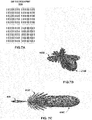
FIGS. 7A - 7C are conceptual diagrams illustrating example radar receive pattern for a collision avoidance system, in accordance with one or more techniques of this disclosure. -
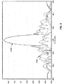
FIG. 8 is a graph illustrating an example radar receive pattern for a collision avoidance system, in accordance with one or more techniques of this disclosure. - This disclosure describes various techniques related to collision avoidance systems and antennas for use in such collision avoidance systems. A collision avoidance system in accordance with the techniques of this disclosure uses radar to detect unwanted objects in a coverage area, and in response to detecting an unwanted object in the coverage area, send a notification to an operator. In one example, a collision avoidance system of this disclosure may be installed on an airplane, and the coverage area may be the area surrounding a wingtip or nose of the aircraft. In another example, a collision avoidance system of this disclosure may be installed on a sea vessel, and the coverage area may be all or a portion of the area surrounding the vessel. As will be explained in more detail below, in order to constrain the coverage area to a desired area that is large enough to adequately detect potential hazards but still small enough to not yield a large number of false positives, a radar collision avoidance system of this disclosure includes an antenna that utilizes digital beam forming. The antenna may further utilize electromagnetic band-gap isolation, a substrate integrated waveguide (SIW), and other such features.
- The collision avoidance system, including both the antennas and associated electronics, is implemented into a single integrated package. The single integrated package may, in many instances, be small enough and light weight enough to be installed in a variety of locations such as in the radome at the top of the vertical stabilizer of an aircraft. Additionally, the collision avoidance system may communicate wirelessly with a display or user terminal such that the collision avoidance system can be installed without the need for long wiring runs. In other examples, the collision avoidance system may implement other techniques to communicate with other systems, such as a user terminal, flight information system, vehicle information system, railroad or automobile traffic management system or similar. The collision avoidance system may communicate with others systems using optical, wired (e.g, Ethernet, USB, etc.), or other similar connections or communications mediums.
-
FIG. 1A is a conceptual diagram illustrating an example coverage area of a collision avoidance system mounted on an aircraft.FIG. 1A depictsaircraft 10 with an example collision avoidance system, which may be mounted in or onvertical stabilizer 16 ofaircraft 10. The example collision avoidance system may be configured to detect objects in a leftradar coverage area 12L and a rightradar coverage areas 12R (collectively "radar coverage area 12"). Radar coverage area 12 may include an area approximately 80 degrees wide. Information from the collision avoidance system may combine with information from a weather radar system that may be mounted in the nose radome ofaircraft 10. The full weather radar system carried in the nose of the aircraft may be used during ground operation to cover a region between 120 and 180 degrees wide from the nose location. - The example collision avoidance system may additionally be configured to communicate, for example via Wi-Fi, over
communication area 14. The illustration ofcommunication area 14 represents only one example of a communication area. Other sizes and shapes of communication areas may also be used. The Wi-Fi communication area 14 may be generated by communication circuitry within the collision avoidance system. The communication circuitry may receive target detection information from targets detected within radar coverage area 12 and transmit target detection information to at least one external display withincommunication area 14. Wi-Fi coverage area may also be described a wireless local area network (WLAN) datalink. The collision avoidance system may transmit signals within Wi-Fi communication area 14 to external displays withinaircraft 10, or to other displays outside ofaircraft 10. For example, one or more safety observers, or "wing walkers" helping to guideaircraft 10 during ground operations may carry display units that may receive target detection information from the collision avoidance system. - A collision avoidance system may also be installed near the passenger gate at an airport to assist in guiding an aircraft to the terminal. In this taxi guidance example, the collision avoidance system may communicate with other devices, such as display devices, using wireless or wired communication techniques.
- Other example applications for the collision avoidance system may include use on helicopters for collision avoidance and landing assistance in a degraded visual environment (DVE) such as blowing dust or snow. An unmanned aerial vehicle (UAV) may include a collision avoidance system. A collision avoidance system may be mounted on a train or at a railroad crossing to notify the train operators, or railroad traffic management, of potential obstacles. A collision avoidance system may be used on a sea vessel for guidance during restricted maneuvering, such as entering or exiting port or transiting a channel or canal. The collision avoidance system on a sea vessel may also be used as early warning when faced with the risk of piracy in certain areas of the world. Although the techniques of this disclosure will primarily be described with reference to an aircraft, it should be understood that the techniques described herein are not limited to aircraft and can be implemented on other types of vehicles and vessels, as well as on stationary structures as well.
-
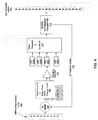
FIG. 1B is a conceptual diagram illustrating a more detailed view of an example position of a collision avoidance system mounted invertical stabilizer 16 ofaircraft 10. The example collision avoidance system may include one or more integrated radar systems mounted in thevertical stabilizer 16 ofaircraft 10.Integrated radar system 18L includes monopulse radar circuitry, a slotted waveguide radar transmit antenna, a slotted waveguide radar receive antenna, and may include external communication circuitry. The various components of the collision avoidance system are housed in a single, integrated package.Integrated radar system 18L may mount in an existing radome on top of thevertical stabilizer 16 ofaircraft 10. In this disclosure the terms "slot waveguide" and "slotted waveguide" may be used interchangeably. The existing radome may be the same radome used by the VHF omnidirectional range (VOR) navigation antenna. The collision avoidance system may include twointegrated radar systems aircraft 10, including coverage beyond both wingtips ofaircraft 10. For example,integrated radar systems FIG. 1B . -
Integrated radar system 18L may be configured to avoid other structures that may be included in an aircraft vertical stabilizer. For example, some vertical stabilizers may include a conductive strip that is part of a lightning strike protection system. Also, in some examples, a vertical stabilizer may include one or more antennae, such as a high frequency (HF) long range communication antenna. A collision avoidance system and integrated radar system configured to not interfere with such structures, as well as configured so these structures do not interfere with the integrated radar system performance, may have advantages over other examples. In one example,integrated radar system 18L may be approximately four inches tall, eight inches long, and one inch thick (4"x 8" x 1"). In other examples, such as on a UAV, the integrated radar system may be smaller. - Also,
integrated radar system 18L may be configured to draw power from existing power within a vertical stabilizer with minimum modification. For example, anintegrated radar system 18L may be configured to draw power from the existing system already in place within the vertical stabilizer. As the collision avoidance system would have the largest advantage during ground operations, such as taxiing, an integrated radar system that drew power from an existing system, only used on the ground, would have advantages over other examples. For example, the integrated radar system could draw power from a taxi lighting system, used only during ground operations. -
FIG. 2A is a conceptual and assembly diagram illustrating an exploded view of an example integrated radar system, which may be a component of a collision avoidance system in accordance with one or more techniques of this disclosure.FIG. 2A illustrates an exampleintegrated radar system 100 which may include a SIW Tx antenna and a protective cover orshield 104.Integrated radar system 100 may, for example, be the same type of integrated radar system asintegrated radar system FIG. 1B . In the example ofFIG. 2A , the integrated radar system is implemented as a multi-layer printed circuit board (PCB) 101 that includes anSIW antenna layer 102 and one or more circuit layers 103. Circuit layers 103 may include 8-channel receiver chips 108A - 108D, analog-to-digital (A/D)converters 106A - 106D as well as other circuit elements. An analog-to-digital converter may also be called an "ADC." -
Multi-layer PCB 101 includes circuits and components that implement radar transmitter electronics, radar receiver electronics, one or more processors, and may further include communication electronics, power conditioning and distribution, clock/timers and other circuitry and components. The one or more processors are configured to control the radar transmitter electronics and radar receiver electronics as well as process and identify radar targets and send notifications and information to users using the communication electronics. A processor may include, any one or more of a microprocessor, a controller, a digital signal processor (DSP), an application specific integrated circuit (ASIC), a field-programmable gate array (FPGA), a system on chip (SoC) or equivalent discrete or integrated logic circuitry. A processor may be integrated circuitry, i.e., integrated processing circuitry, and that the integrated processing circuitry may be realized as fixed hardware processing circuitry, programmable processing circuitry and/or a combination of both fixed and programmable processing circuitry. - The
SIW antenna layer 102 may be electrically connected to circuit paths and components on one or more circuit layers 103. In some examples, plated vias may provide connections between one or more circuit layers 103, as well as toSIW antenna layer 102. A via may be a plated or unplated hole that may be drilled, etched or otherwise formed between layers ofmulti-layer PCB 101. A plated via may be plated with a conductive material to electrically connect layers. Some examples of conductive material may include copper, solder, conductive epoxy or other materials. -
Protective shield 104 may cover and provide structural support for exampleintegrated radar system 100.Protective shield 104 may be a molded plastic, stamped or formed sheet metal or other suitable material.Protective shield 104 may include a conductive coating in one or more areas to provide shielding for electromagnetic interference (EMI).Protective shield 104 may include penetrations for power, communication or other connections as well as be configured to securely mountintegrated radar system 100. - In operation,
integrated radar system 100 provides digital electronic beam steering on received radar reflections, for example by using, in part, phase shift commands within the components on one or more circuit layers 103. The radar transmitter electronics, in signal communication with the radar transmit antenna, are configured to output, e.g., transmit, monopulse radar signals that are a fixed, wide beam illumination. The radar receiver electronics in signal communication with the radar receive antenna search the reflected radar signals by a "pencil beam" monopulse receive pattern that scans within the illuminated transmit area. In other words,integrated radar system 100, is a frequency modulated continuous wave (FMCW) dual antenna radar system that provides wide beam illumination on transmit and then an electronically scanned receive beam that searches within the wide transmit illumination area. The FMCW radar signals provide very fine range resolution and allows very low receiver bandwidth and low data rates. This includes resolution in all three dimensions. In other words,integrated radar system 100 may locate the X, Y and Z position of possible collision threats. Locating the height of a target may have the advantage of reducing false alarms. For example, the collision avoidance system may detect an object that will pass under the wings but be at a height that will pose no danger to the wings, engine nacelles or other portions of an aircraft. - The digital electronic beam steering at baseband frequencies provides the advantage of reduced cost and complexity because of fewer radio frequency (RF) components. Digital electronic beam steering may also be capable of receiving multiple simultaneous beams.
- In one example,
integrated radar system 100 may use a heterodyne FMCW radar with a 16 MHz first intermediate frequency (IF) before down conversion to a baseband between 1 KHz and 2 MHz.Integrated radar system 100 may apply the 16 MHz offset using a dual direct digital synthesis (DDS) at the transmit array. A heterodyne system may provide advantages over other FMCW radars that use a homodyne receiver to directly convert RF signals to baseband near zero frequency.Integrated radar system 100 may include components with a passband that includes 16 MHz. These components may also provide simultaneous down conversion to base band, I / Q channel formation and four-bit phase shift. By using multi-function components along with frequency down conversion,integrated radar system 100 may provide advantages over a standard homodyne receiver, even if the homodyne receiver used an I/Q mixer on receive. In this way,integrated radar system 100 may achieve performance advantages. A few examples include I/Q accuracy (true 90 degree offset), four-bit phase shift, fine range and elevation resolution, low receiver bandwidth, low data rates, small size, light weight, low power consumption, integrated package and easy retrofit of existing platforms. -
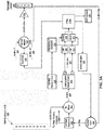
FIG 2B is a conceptual diagram illustrating the transmission, receive and communication antennae of an example integrated radar system, which may be a component of a collision avoidance system in accordance with one or more techniques of this disclosure.FIG. 2B illustrates a more detailed view of the radiating and receiving portion ofSIW antenna layer 102 shown inFIG. 2A .SIW antenna layer 102 may include a Wi-Fi antenna 120, an SIW receiver (Rx)array 122, anisolation area 124 and an SIW transmit (Tx)antenna 126.SIW Rx array 122 may include one or more radar receiver antenna subarrays 132A - 132D. Each subarray may include anSIW antenna device 130. In the example ofFIG. 2B , eachsubarray 132A - 132D contains eight SIW antenna devices. For clarity,FIG. 2B only showsSIW antenna device 130 with a number.SIW antenna device 130 may also be referred to as a slotted waveguide antenna device. Therefore,SIW Rx array 122 may be considered a slotted waveguide radar receive antenna.SIW Tx antenna 126 may be considered a slotted waveguide radar transmit antenna. -
SIW Tx antenna 126 may include one or more SIW Tx antenna devices 134A and 134B (collectively SIW Tx antenna device 134). Each SIWTx antenna device 134 may be similar toSIW antenna device 130 in construction and function. SIW Tx antenna 126 (or slotted waveguide radar transmit antenna) may be in signal communication with the radar transmitter electronics. The radar transmitter electronics, in conjunction with the slotted waveguide radar transmit antenna, may be configured to output radar signals to a predetermined coverage area. The predetermined coverage area may be similar to radar coverage area 12 shown inFIG. 1A . The terms radar transmit electronics and radar transmitter electronics may be used interchangeably in this disclosure. - SIW Rx array 122 (or slotted waveguide radar receive antenna) may be in signal communication with radar receiver electronics. The radar receiver electronics includes digital beam forming circuitry configured to receive radar reflections corresponding to the outputted radar signals from the radar receive antenna. The outputted radar signals may reflect off objects present in the predetermined coverage area. The radar receiver electronics sends information to the one or more processors about the reflected signals from objects present in the predetermined coverage area. The one or more processors are configured to generate a notification in response to a radar reflection received from the first coverage area.
-
Isolation area 124 may be used to isolate the outputted radar signals coming fromSIW Tx antenna 126 from interfering withSIW Rx array 122.Isolation area 124 may have dimensions and be composed of material to ensure proper function ofintegrated radar system 100. For example,isolation area 124 may be a structure such as an electronic band gap structure or an absorptive structure. The dimensions and/or material may vary depending on the operating frequency ofintegrated radar system 100. - Wi-
Fi antenna 120 may be configured to transmit and receive signals used to communicate using a wireless local area network (WLAN). Wi-Fi antenna 120 may be communicatively coupled to electronic communication circuitry withinintegrated radar system 100 configured to receive information from one or more processors withinintegrated radar system 100. For example, the electronic communication circuitry may be part ofmulti-layer PCB 101. The electronic communication circuitry, in conjunction with Wi-Fi antenna 120 may be configured to communicate with display units or other units external tointegrated radar system 100. Some examples of external display units may include tablet computers or hand-held mobile devices. -
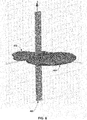
FIG. 3A is a three-dimensional view illustrating an example SIW element in accordance with one or more techniques of this disclosure.SIW element 131 may be a component ofSIW antenna device 130 shown inFIG. 2B .SIW element 131 may include aradiating slot layer 140, afirst SIW portion 142, aground layer 144 and asecond SIW portion 150.SIW element 131 may be configured to operate with a first radio-frequency (RF) energy of a first wavelength (Aλg), where Aλg is the wavelength of the first RF energy inside the SIW material and Aλ is the wavelength of the first RF energy in free space. - The
first SIW portion 142 may include two or more rows ofvias 152. Each via may be a plated via, that is, the inner surface of each via may be plated with a conductive material such as copper. Dimensions for vias as well as spacing and relationship to slots in radiatingslot layer 140 will be discussed in more detail inFIG. 3D below. - Radiating
slot layer 140 may form a first layer of each SIW and may be electrically connected to, but not penetrated by each via 152. Radiatingslot layer 140 may include a plurality of slots arranged in a row ofslots 141. The row ofslots 141 may run parallel to the rows ofvias 152 and between each row of vias. Each slot of the plurality of slots may penetrate radiatingslot layer 140.Ground layer 144 may form a second layer of the first SIW portion and may be electrically connected to, but not penetrated by each via 152. Therefore,ground layer 144 may be electrically connected to radiatingslot layer 140. -
Second SIW portion 150 may include two or more rows ofvias 152A andmicrostrip transition 148.Second SIW portion 150 may bond to groundlayer 144.Vias 152A may electrically connect to, but not penetrateground layer 144. Therefore, vias 152A, vias 152,ground layer 144 and radiatesslot layer 140 are electrically connected. Moreover, vias 152A, vias 152 may be considered 'blind holes,' in that the holes connect, but do not penetrate a metal layer, such asground layer 144. Therefore, the vias on different layers may be configured to overlap vertically. In other words, the vias may be configured to line up with each other, but without physically connecting. This arrangement may have advantages in a variety of applications, because, for example, the arrangement may offer flexibility in circuit layout. Bothfirst SIW portion 142 andsecond SIW portion 150 may include one or more bondply layers. -
Microstrip transition 148 may have specific dimensions and shape that depend on the signal frequency.Microstrip transition 148 may be positioned in relation tocoupling slot 146 such thatmicrostrip transition 148 stimulatescoupling slot 146. -
Coupling slot 146 may penetrateground layer 144.Coupling slot 146 may connectfirst SIW portion 142 tosecond SIW portion 150. In some examples,SIW element 131 is a receive element. Reflected radar signals impinging on radiatingslot layer 140 may penetrate tofirst SIW portion 142.First SIW portion 142 may guide any received RF energy from the reflected radar signals tocoupling slot 146.Coupling slot 146 may couple the RF energy further tosecond SIW portion 150. In other examples,SIW element 131 is a transmit element.Second SIW portion 150 may receive RF energy from the radar transmitter electronics and couple the RF energy tofirst SIW portion 142 throughcoupling slot 146. -
Terminal edge 154 may penetratesecond SIW portion 150,ground layer 144 andfirst SIW portion 142. The example ofFIG. 3A depictsterminal edge 154 as a slot passing between the layers. In this example, the slot may be plated with a conductive material, such as copper. The long edge ofterminal edge 154 may be perpendicular to the row ofvias 152.Terminal edge 154 may electrically connect, but not penetrate radiatingslot layer 140. Therefore,terminal edge 154 may electrically connect radiatingslot layer 140 toground layer 144. Specific dimensions forterminal edge 154, spacing and physical location relative to other features ofSIW element 131 will be discussed in more detail below, such asFIG. 3D . - The SIW may be constructed of copper clad PCB for the upper and lower waveguide surface, with the dielectric of the PCB for the waveguide volume and plated vias (aka holes) for the waveguide walls. In other words, SIW is a transmission line that creates a waveguide within a substrate. Its waveguide consists of two lines of holes as the wall of rectangular waveguide and the metallic layer on the top and bottom to form a rectangular cavity. The SIW waveguide suffers higher insert loss than aluminum waveguide caused by (a) the substrate, (b) the gap between holes and (c) the surface roughness between metallic layer and the substrate. But it brings a lot of advantages to develop radar system such as mono-pulse radar that generally requires 4 antenna beams. Some advantages include, SIW makes the rectangular waveguide very thin and light, it benefits many mechanically steered antennas as its lower weight and relatively small moment of inertia. An SIW antenna is a PCB version of a slotted waveguide antenna. An SIW antenna may have advantages over other types of slotted waveguide antennae, such as a slotted waveguide antennae constructed from aluminum. For example, the substrate filled in SIW structure makes it is possible to put more slots in one branch, thereby the SIW antenna array is able to offer a tight, narrow beam-width that is beneficial to many applications.
- Some examples of SIW monopulse antenna array may have many difficulties. These may include the strong mutual coupling between slots, the difficulty in layout and positioning, the complex estimation of its equivalent guide wavelength and the difficulty of consistent manufacture, along with other difficulties. SIW antennae using the techniques of this disclosure may result in a SIW monopulse antenna array that is highly integrated, highly shielded, easy to manufacture and reliable.
-
FIG. 3B illustrates a section of an example slot waveguide antenna array system with a separate mixer for each channel.FIG. 3B illustratesexample SIW element 131 along with additional components, which may be part of an integrated slot waveguide antenna array system. As shown inFIG. 3A ,SIW element 131 may include radiatingslot layer 140,first SIW portion 142 andsecond SIW portion 150. Other components ofSIW element 131, such asground layer 144, omitted for clarity.FIG. 3B depicts additionalelements including mixer 164 andthird SIW portion 158.FIG. 3B also depicts anexample cross section 160 of an example SIW antenna device andantenna subarray layout 162.Example cross section 160 illustrates radiatingslot layer 140,first SIW portion 142,ground layer 144, a signal layer and an additional substrate and ground layer.Example cross section 160 illustrates a four-layer PCB, with a slot layer, a ground layer, a signal layer and a second ground layer with substrate in between each metal layer. In other examples,cross section 160 may illustrate a three-layer, five-layer or more layers. -
Antenna subarray layout 162 may include eight SIW antenna devices, similar toSIW antenna device 130 shown inFIG. 2B . Each SIW antenna device may be dedicated to a separate radar channel.Antenna subarray layout 162 may also include amixer 164A for each device/channel and an eight-way power divider (PD) 176. Example ofantenna subarray layout 162 illustrates eight-way power divider 176 as laid out on the signal layer, as shown incross section 160. Eight-way power divider 176 may be configured so each path length from the local oscillator (LO) is the same length. This may ensure the signal from the LO, such as a voltage controlled oscillator (VCO), arrives at eachmixer 164A at the same time and with the same phase. -
Third SIW portion 158 may include vias 152C and twomicrostrip transitions Vias 152C may be a different diameter and spacing thanvias 152 and be configured to operate at a different RF energy than that used by the first SIW portion and the second SIW portion.Third SIW portion 158 may be configured to operate with an RF energy of a different wavelength and frequency.Third SIW portion 158 may connectmixer 164 to eight-way power divider 176 depicted inantenna subarray layout 162. The area ofthird SIW portion 158 may provide space for asignal transfer area 165.Signal transfer area 165 may carry signals such as output ofmixers 164, control signals and other signals.Signal transfer area 165 may also include electronic components that may interact with signals carried by signal traces onsignal transfer area 165. In one example, not shown inFIG 3B , the output ofmixers 164 may reach the signal transfer area using conductive vias different and distinct fromvias FIG. 3B , the power divider is on a metal layer ofmulti-layer PCB 101, rather than a waveguide, as may be found in other examples. A power divider on the metal layer may provide advantages in cost, manufacturability, reliability as well as allow a smaller size for the radar system. -
FIG. 3C illustrates a section of an example slot waveguide antenna array system with a four-channel mixer and single SIW portion connecting the mixer to a power divider and a local oscillator (LO).FIG. 3C may be similar toFIG. 3B except instead of a separate mixer for each channel, the example ofFIG. 3C depicts a four-channel mixer FIG. 3C also depicts an exampleantenna subarray layout 170 with eight antenna devices/channels, similar toantenna subarray layout 162, except example ofFIG. 3C connects the LO to two four-channel mixer components and therefore only needs the two-way PD. The two-way PD shown inFIG. 3C operates to connect the local oscillator (LO) tomixer 172, similar to the eight-way PD 176 forFIG. 3B . Because the example ofFIG. 3C includes fewer mixers and fewer PD circuit traces, this may allow more space on the layers above and belowthird SIW portion 168 for additional components and/or space for additional circuit traces or components. In other words, becausethird SIW portion 168, which may includeSIW elements third SIW portion 158,signal transfer area 165A may be larger than the similarsignal transfer area 165. This may allow additional space for components or for traces to carry signals, for example inhardware component region 166. The terms "circuit trace", "trace" or "circuit path" may be used interchangeably in this disclosure. - Similar to the layout for eight-way power divider 176 shown in
FIG. 3B ,FIG. 3C illustrates example two-way power divider 176A with equal length paths. This may ensure the signal from the LO, such as a VCO, arrives at eachmixer 172A at the same time and with the same phase. -
FIG. 3D is a two-dimensional view of an example SIW element illustrating dimensions and spacing in accordance with one or more techniques of this disclosure.FIG. 3D depicts a SIW defined by rows of plated vias orholes 152D. In this disclosure hole, plated hole, via and plated via may be used interchangeably, unless otherwise specified.FIG. 3D defines the spacing between centerline of adjacent holes in each row to be substantially equal, where substantially equal means equal within manufacturing tolerances. In other words, the spacing between adjacent holes in the same row is equal, plus or minus any variations in manufacturing. For example, dl= d2 as shown inSIW power divider 190. Note thatSIW power divider 190 is different from the eight-way PD 176 and two-way PD 176A described above.SIW power divider 190 is a power divider implemented in SIW material and construction. The eight-way PD and two-way PD described above are implemented on a circuit layer or signal layer and may be of metal or other conductive material.SIW power divider 190 is another example of an SIW layout in accordance with the techniques of this disclosure.SIW power divider 190 is not shown inFIGS. 3A - 3C . - The equal distance between hole centerline d1 and d2 may be divided evenly by ¼ equivalent guide wavelength according to the equation (N∗d=1/4 λg). In the example of
FIG. 3D , the equal hole spacing may be defined as 1/8 λg. In other words, the via spacing may be selected to operate for a particular wavelength/frequency of RF energy. Therefore, for each row of vias 152D, a centerline of each via in the first row of vias may be ⅛Aλg from the centerline of an adjacent via in the first row of vias. Similarly, a centerline each via in the second row of vias of may be ⅛Aλg from the centerline of an adjacent via in the second row of vias. - The example of
FIG. 3D defines the SIW waveguide width (a) as even multiple of the equal distance (d) between the centerlines of each row of vias according to the equation a = (2n)∗d. For example, selecting n =3 results in an SIW width a = 6d (182). Selecting the SIW width a = 6d results in ahole 183 in the center of the short edge, as shown inSIW power divider 190. This may have performance advantages over other selections. As shown inFIG. 3D , the first row of vias is substantially parallel to the second row of vias and a centerline of the first row of vias is ¾Aλg = 6d (182) from a centerline of the second row of vias. Here, substantially parallel means parallel within manufacturing tolerances. In other words, the centerline of the first row is parallel to the centerline of the second row, plus or minus any variations in manufacturing. - Variations and tolerances apply throughout this disclosure. For example,
SIW width 182 described above as a = 6d should be understood to mean a = 6d ± tolerances from manufacturing or other sources. -
FIG. 3D also depicts a row of radiating slots. By selecting the length, spacing and position of each radiating slot in the row of radiating slots, the reflection around each slot can be the same, that is, by repeating four holes for each ½ λg (181).FIG. 3D depictsfinal radiating slots 184A - 184C in the row of radiating slots. In other words, selecting each radiating slot to have the same length and spacing, and placing a long-edge centerline of the final radiating slot, such as 184C, to be ¼Aλg from the terminal edge186C may result in a four-space (4d) reflection zone from the plated vias on either side of each radiating slot.FIG. 3D depicts this four-space reflection zone by theitem 181, which shows 4d e.g. four equal spaces between holes, from centerline to centerline along the radiating slots. - Similarly, for alternative examples of
terminal edges 186A (a row of vias) and 186B (a plated slot), placingfinal radiating slots -
FIG. 3E is a three-dimensional view of an example SIW power divider.FIG. 3E depicts exampleSIW power divider 190, which is configured the same asSIW power divider 190 shown inFIG 3D . Example,SIW power divider 190 as depicted byFIG. 3E includesvias 152D, an SIW width a = 6d (182), which results in ahole 183 in the center of the short edge.FIG. 3E also depicts three microstrip transitions, though for clarity onlymicrostrip transition 148C is labeled.FIG. 3E illustrates a three-dimension view of an example implementation of an SIW power divider. SIW power divider is distinct frompower dividers 176 and 176A in thatpower dividers 176 and 176A may be implemented on a circuit layer of anexample multi-layer PCB 101, whereSIW power divider 190 may be implemented on an SIW layer. -
FIG. 3F is a two-dimensional view of an example slot waveguide antenna array system illustrating dimensions for a coupling slot and microstrip in accordance with one or more techniques of this disclosure. Each channel may have a coupling slot 146E. The distance between the short-edge centerline of coupling slot 146E toterminal edge 154E may be given according to the equation:
FIG. 3F depictsterminal edge 154E as a plated slot. The distance betweenmicrostrip transition 148E andterminal edge 154E may be given according to the equation:
- For a digital active phased array, a longer Dc and DT suffers higher insert loss than a shorter Dc and DT. However, a larger Dc and DT provides additional space to put additional components on other layers. In other words, n > 1, provides more space for additional components. The example of
FIG. 3F depicts n = 1 to minimize insertion loss resulting in Dc = λgl2 and DT = λg. An SIW slot waveguide antenna with coupling slot location and microstrip location according to the techniques of this disclosure may have advantages for consistent and reliable SIW design and performance. The layout and benefit ((2n-1)/N-1 coupling) may balance loss and enough area for the back circuit. As depicted in the example ofFIG. 3F , the terminal of each SIW element connects to a ground layer,e.g. ground layer 144, using a single plated slot hole (186B) instead of many vias or holes (186A), as shown inFIG. 3D . -
FIG. 3G is a combined three-dimensional view and cross-sectional view of an example multi-layer PCB that may integrate waveguide layers, signal and component layers.FIG. 3G includes examplecross-sectional view 195 with three-dimensional views offirst SIW portion 142B andthird SIW portion 158B. In the example ofFIG. 3G ,first SIW portion 142B andthird SIW portion 158B are configured the same as the examplefirst SIW portion 142 andthird SIW portion 158 as shown inFIG. 3B . -
Cross section view 195 includes substrate layers 196A - 196D and, though not labeled for clarity sake, may also include metal layers described inFIG. 3B , e.g., a slot layer, a ground layer, a signal layer and a second ground layer. The portion of example multi-layer PCB illustrated bycross-section 195 includes RFfront end 198,third SIW portion 158A withvias 152C,first SIW portion 142A withvias 152 and radiatingslot layer 140. The vias, and radiatingslot layer 140, are configured in the example ofFIG. 3G the same as in the example ofFIG.3B , and other figures described above.Coupling slot 146B connectsfirst SIW portion 142A to substrate layer 2 (196B). In some examples,multi-layer PCB 101 may include additional coupling slots between other layers.Microstrip transition microstrip transition 148 described above. -
FIG. 4 is a conceptual and schematic block diagram illustrating an example integrated monopulse radar system using a slot waveguide antenna array system in accordance with one or more techniques of this disclosure.FIG. 4 depicts SIWRx array element 200 andSIW Tx array 202, which function similarly to theSIW Rx array 122 andSIW Tx antenna 126 as shown inFIG. 2B .Rx mixer 204 operates in a manner similar tomixer 164 fromFIG. 3B .Reference signal 218 may be a local oscillator (LO) signal that may pass through a similar eight-way divider as shown inFIG. 3B .Receiver IC 206 andADCs 212A - 212D may be similar to thereceiver chip 108A - 108D and A/D converters 106A - 106D shown inFIG. 2A . An example component that may perform some of the features ofreceiver IC 206 may include the AD9670 Octal Ultrasound Analog Front End (AFE) Receiver, which will be described in further detail below. -
Rx mixer 204 may receive inputs from SIWRx array element 200 andreference signal 218 fromdigital synthesizer transmitter 216 to down-convert the reflected radar signals received by SIWRx array element 200.Rx mixer 204 may output the downconverted radar receive signal to a respective receiver integrated circuit (IC) 206 for a respective receive channel.Receiver IC 206 may output the respective signals for the respective receive channel to a respective ADC, such asADC 212C as shown in the example ofFIG. 4 . - FPGA processor and controller 214 ("
FPGA 214") may receive the digitized signals from the different receivechannel ADCs 212A - 212C.FPGA 214 may perform the functions of digital receive beam steering, target detection processing and analysis and send target information to the external communication system to be further sent to one or more display devices. For example,FPGA 214 may control the radar transmitter electronics, which are configured to output radar signals in conjunction with the SIW radar transmitarray 202. Radar transmitter electronics may includedigital synthesizer transmitter 216. -
FPGA 214 may also control the radar receiver electronics which may includeRx mixer 204, the four receiver integrated circuits (IC) 206, summingamplifier 210 andADCs 212A - 212D. The radar receive electronics may include digital beam forming circuitry configured to receive radar reflections corresponding to the outputted radar signals, and to send signals associated with the radar reflections toFPGA 214. SIWRx array element 200, acts as a radar receive antenna to collect radar reflections impinging on the surface of its slot layer. SIWRx array element 200 may be a singleSIW antenna device 130 in asubarray 132A within theSIW Rx array 122, as depicted inFIG. 2B . The terms radar receive electronics and radar receiver electronics may be used interchangeably in this disclosure. -
FPGA 214 anddigital synthesizer transmitter 216 may include circuitry that converts received radar signals to a lower frequency for further processing. Further processing may include beam steering, target detection and location as well as other functions. Other types of functions performed byFPGA 214 anddigital synthesizer transmitter 216 may include in-phase and quadrature processing (I and Q), filtering, frequency, phase and amplitude control, modulation, direct digital synthesis (DDS) and other functions. The digital beam forming may include heterodyne processing. The digital beam forming circuitry may be configured to operate in the ultrasonic frequency range. -
FIG. 5A is a conceptual and schematic block diagram of an example radar receive channel and radar transmitter electronics that may be used in an obstacle collision avoidance system. The example diagram ofFIG. 5A depicts a single receive channel and an example implementation of superheterodyne up and down converting from RF frequencies to other frequencies. Other receive channels that may be part of a collision avoidance system are not shown inFIG. 5A for clarity. -
FIG. 5A includes additional details of portions ofintegrated radar system 100 using a slot waveguide antenna array shown inFIG. 4 .FIG. 5A may include SIWRx array element 200,SIW Tx array 202 andRx mixer 204 as shown inFIG. 4 . Addition components shown inFIG. 5A may be included in FPGA processor andcontroller 214,digital synthesizer transmitter 216 andReceiver IC 206.FIG. 5A depictsVCO 300, local oscillator (LO)feed network 302 and other receivechannels 304, along with in-phase and quadrature (I and Q)unit 306, low pass filters (LPF) 308 and 312 and analog todigital converters FPGA 214A,synthesizer MHz master clock 324,frequency dividers 326, dual digital direct synthesis (DDS)unit 328, I/Q single side band (SSB)mixer 330, andamplifier 332. Also Wi-Fi system 320, which may receive information fromFPGA 214A. - The radar receiver electronics depicted in
FIG. 5A down-convert received radar signal from SIWRx array element 200 to an intermediate frequency (IF) 16 MHz (340) and to lower frequencies for further processing, which may include receive beam steering. The radar transmitter electronics may transmit RF energy with a wide azimuth and narrow elevation through transmit (Tx)array 202. -
VCO 300, as shown in the example ofFIG. 5A , generates a 24 GHz signal which is distributed to theLO feed network 302 and further toRx mixer 204.LO feed network 302 may function, for example, as an eight-way power divider 176 or two-way power divider 176A as shown inFIGS. 3B and3C .VCO 300 also distributes 24 GHz to I/Q SSB mixer 330.VCO 300 may receive input fromsynthesizer 322. 24 GHZ is shown as one example. Inother examples VCO 300 may generate other frequencies, such as 13 GHz. -
LO Feed network 302 may output the 24.0 GHz LO signal to other receivechannels 304 as well asRx mixer 204, which functions the same asRx mixer 204 shown inFIG. 4 . In the example ofFIG. 5A ,Rx mixer 204 converts the 24.016 GHz reflected radar signal from SIWRx array element 200 to an intermediate frequency (IF) of 16 MHz (340). These frequency values are only for illustration.Integrated radar system 100 may also use other frequencies.Rx mixer 204 may output the IF of 16 MHz (340) to I andQ unit 306. -
Synthesizer 322 may utilize a method of changing the division ratio within a digital PLL synthesizer to provide frequencies that are not integral multiples of the comparison frequency. A divider may take a fractional division ratio rather than an integer ratio by alternating between division ratios. One example may include a fractional N synthesizer that uses the basic digital PLL loop. Analog Devices component ADF4159, a direct modulation fractional-N frequency synthesizer, is one example of a fractional N synthesizer. However, in some examples fractional N synthesizers may generate spurious signals that appear as false targets in the receiver. Other example ofsynthesizer 322 may include a direct digital synthesizer that may have advantages over a fractional N synthesizer. - Frequency synthesis may use various forms of Direct Digital Synthesizer, Phase Lock Loop, frequency multiplier and other methods.
Synthesizer 322 will generate a linear FMCW waveform and may receive control and other inputs fromFPGA 214A. - I and
Q unit 306 may include a phase shift function along with the in-phase and quadrature function. A monopulse radar may need to get information both from the real and imaginary portions of the returned radar signal. I andQ unit 306 may provide a representation of the returned radar signal at the intermediate frequency (IF) of 16 MHz, as shown inFIG. 5A . These frequencies listed inFIG. 5A are just for illustration. Other frequencies may also be used. The quadrature down conversion may divide the 128 MHz oscillator signal by eight, e.g. 8 x 16 MHz = 128 MHz. Terms for 128MHz master clock 324 may include reference oscillator, 128 MHz oscillator and 128 MHz clock. These terms may be used interchangeably in this disclosure. - I and
Q unit 306 may perform two functions simultaneously. First, I andQ unit 306 may divide 128MHz clock signal 324 by eight and provide a four-bit phase shift with digital control. At the same time as the four-bit phase shift, I andQ unit 306 may form the in-phase (I) and quadrature (Q) signal portions and downconvert the 16 MHz IF frequency to a base band between 1 kHz and 2 kHz. The I and Q signal portions may also be called the "I" channel and "Q" channel. The output signal from I andQ unit 306 passes throughLPF ADCs ADCs frequency dividers 326. Bothfrequency dividers 326 and I andQ unit 306 may receive a 128 MHz clock signal from 128MHz master clock 324.Frequency dividers 326 may output a signal toADCs -
FPGA 214A may receive the separate I and Q signals from each receiver channel.FPGA 214A may combine and process the signals, including digital receive beam steering to determine the 3D position of obstacles within the radar coverage area, as shown inFIG. 1A .FPGA 214A may process obstacle information, including size, height, rate of closure and other information and send to Wi-Fi system 320. Wi-Fi system 320 may further send obstacle information of one or more display devices. One possible example ofFPGA 214A may include the Xilinx XC7k70t 7-series FPGA. - Radar transmitter electronics may include
dual DDS 328 and I/Q SSB mixer 330.Dual DDS 328 may receive commands and control inputs fromFPGA 214A and output a 16MHz intermediate frequency I signal 334 and Q signal 336 to I/Q SSB mixer 330. An example dual DDS may include the Analog Devices AD9958. - I/
Q SSB mixer 330 may receive the signals fromdual DDS 328, as well as a 24GHz signal fromVCO 300. I/Q SSB mixer 330 may output radar signals toamplifier 332 and further to SIW transmitarray 202. One example ofamplifier 332 may include the HMC863 from Analog Devices. SIW transmitarray 202 may output the radar signals in the prescribed pattern. Any reflected radar signals may impinge on SIWRx array element 200 and be conducted to the FPGA for processing. -
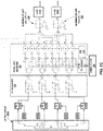
FIG. 5B is a conceptual block diagram of portions of an example receive module illustrating multiple channels that may be part of radar receive electronics in accordance with one or more techniques of this disclosure.FIG. 5B illustrates example components and techniques to process received radar signals from a portion ofSIW receiver array 122 as shown inFIG. 2B . The example ofFIG. 5B depicts other details of the functions ofFIG. 4 andFIG. 5A that include an exampleradar receiver subarray 132A, such as that shown inFIG. 2B . A complete, integrated radar system may use one or more sets of the components shown inFIG. 5B . For example, an integrated radar system that uses four radar receiver subarrays may use four sets of components as shown inFIG. 5B to achieve the 32 channels shown inFIG. 2B . - Receive
module 350 may include radarreceiver antenna subarray 132A,VCO 300, anRx mixer 204A - 204H for each channel, an octal analog front end (AFE)receiver 352, a summing operational amplifier (opamp) and LPF for both in-phase 354 ("I") and quadrature 356 ("Q") signals, a dual channel low voltage differential signaling (LVDS)unit 358,FPGA clock dividers 360 andvoltage regulators 362. The components depicted in receivemodule 350 may be mounted and inter-connected onmulti-layer PCB 101 that includes a,SIW antenna layer 102 and one or more circuit layers 103, shown inFIG. 2A . - The example of
FIG. 5B depicts radarreceiver antenna subarray 132A to include eight SIWRx array elements 200A - 200H. In other examples,radar receiver subarray 132A may include more or less than eight SIW Rx array elements. Each SIWRx array element 200A - 200H connects to arespective Rx mixer 204A - 204H. EachRx mixer 204A - 204H for each of the eight channels depicted in receivemodule 350 also receive a 24 GHz LO signal fromVCO 300. The Rx mixers down-convert the reflected radar signal received by the SIW Rx array element for each channel and send the input tooctal AFE receiver 352. The signal path for each channel may include components other thanRx mixers 204A - 204H, as depicted byFIGS. 4 ,5A and below inFIG. 5C . The example ofFIG. 5B depicts anRx mixer 204 for each channel. Other examples may use a four-channel mixer rather than a single mixer for each channel. Example four-channel mixer components may include the ADF5904 from Analog Devices. As described above, mixer components may have performance advantages when placed in the middle of the SIW subarrays so that the path lengths between each subarray and the four-channel receiver chip is equal length. For example, this may allow the signal fromVCO 300 to arrive at the same time and in the same phase for each receiver channel. -
Octal afe receiver 352 may perform a variety of functions for each of the eight channels. Some examples may include preamplification, harmonic rejection, anti-alias filtering, I/Q demodulation and phase rotation, digital demodulation and decimation as well as conversion to digital signals through ADC. One possible example component to perform at least some of the functions ofoctal afe receiver 352 may include the Analog Devices AD9670 Octal Ultrasound Analog Front End (AFE) Receiver.Octal afe receiver 352 may receive a 128 MHz clock input from 128MHz master clock 324.Octal afe receiver 352 may output an in-phase "I" signal for each channel to a set of summing opamp and low pass filters for each channel, depicted as asingle unit 354 in the example of receivemodule 350. Similarly,Octal afe receiver 352 may output a quadrature "Q" signal for each channel to a set of summing opamp and low pass filters for each channel, depicted as asingle unit 356. -
LVDS unit 358 may receive the "I" and "Q" inputs from summing opamp and low pass filters 354 and 356 as well as an input fromFPGA clock dividers 360.LVDS unit 358 may operate under the LVDS, or TIA/EIA-644 technical standard to sample the input signals and perform analog-to-digital conversion. Example components that may perform one or more functions ofLVDS unit 358 may include Analog Devices AD7357 or AD7356 differential input ADC components.LVDS unit 358 may output the digitized "I" and "Q" signals for further processing, such as beam forming, obstacle identification and other functions as needed by a collision avoidance system, in accordance with one or more techniques of this disclosure. - Receive
module 350 may also includevoltage regulators 362.Voltage regulators 362 may provide regulated power supplies to the components of receivemodule 350. For example,LVDS unit 358 may require an input voltage of 2.5V whileoctal AFE receiver 352 may require an input voltage of 3.0V. Voltage regulators 362 may supply power for proper operation of each component in receivemodule 350. -
FIG. 5C is a conceptual and schematic diagram depicting additional details of a portion of the radar receive electronics that may be included in an integrated radar system.FIG. 5C depicts four channels of example radar receive electronics for clarity. In the exampleSIW receiver array 122 as shown inFIG. 2B , the set of electronics depicted inFIG. 5C would be repeated for the total number of channels in the receive array.FIG. 5C retains the same numbers for components where components inFIG. 5C are the same as in other figures. For example, SIWRx array elements 200A - 200D and 128MHz master clock 324 are the same as those components shown inFIG. 5B . -
FIG. 5C illustrates some of the additional components that may be included in the radar receiver electronics, which may be mounted and interconnected onmulti-layer PCB 101.FIG. 5C depictsLO feed network 302A,Rx mixers 204A - 204D, SIWRx array elements 200A - 200D, intermediate frequency (IF) low-noise amplifier (LNA) and high pass filter (HPF) 370,octal AFE receiver 352, summing opamp andLPF ADC 314A and "Q"ADC 310A. Also shown in the example ofoctal AFE receiver 352 isquadrature divider 372 and serial data in (SDI)controller 374. -
LO feed network 302A may deliver a 24 GHz oscillator signal toRx mixers 204A - 204D.LO feed network 302A may receive as input the 24 GHz LO signal from a VCO, such asVCO 300, not shown inFIG. 5C , but shown in 5A. The example ofFIG. 5C depictsLO feed network 302A configured so each path length from the local oscillator (LO) is the same length. This may ensure the signal from the LO, such as a VCO, arrives at eachRx mixer 204A - 204D at the same time and with the same phase. This is similar to eight-way power divider 176 shown inFIG. 3B . -
Rx mixers 204A - 204D function the same as described above by receiving and downconverting the reflected radar signals from SIWRx array elements 200A - 200D.Rx mixers 204A - 204D output the downconverted signals to the respective channels of IF LNA and HPF 370 (referred to as "LNA 370" for clarity).LNA 370 outputs each channel to a respective channel ofoctal AFE receiver 352. In the example of an FMCW radar, the high pass filter may set the frequency response of the receiver. A high pass filter is used to set the IF response to have a 40dB per decade response over a frequency range of about 1 KHz to 2MHz. This function exactly offsets the propagation losses as a function of range. -
Octal AFE receiver 352 functions the same as described above. Also depicted inFIG. 5C isquadrature divider 372, which helps with the phase shift function that creates the "Q" output for the monopulse radar receive signals.SDI controller 374 may help manage the data flow to the summing op amps. - Summing opamp and
LPF LPF - "I" ADC 341A and "Q"
ADC 310A perform the same function for the I and Q ADCs described above. "I" ADC 341A and "Q"ADC 310A digitize the four channels of downconverted and filtered radar receive channels and output the digitized signals for further processing, as described above. -
FIG. 6 is a conceptual diagram illustrating an example radar transmission pattern for a collision avoidance system, in accordance with one or more techniques of this disclosure.FIG.6 includes an example transmitantenna 400, a wide azimuth, narrow elevationmain transmission beam 404 andsidelobes 402. The radar transmitter electronics, in conjunction with the radar transmitantenna 400, may be configured to output radar signals comprising a transmitted radar beamwidth of less than eight degrees in elevation and at least 65 degrees in azimuth. Radar transmitantenna 400 may function in a similar manner to SIW transmitarray 202 shown inFIG. 4 andSIW Tx antenna 126 shown inFIG. 2B . The example SIW transmit pattern may include low elevation sidelobes, which may have the advantages of preventing false alerts and erroneous detections. -
FIGS 7A - 7C are conceptual diagrams illustrating example radar receive pattern for a collision avoidance system, in accordance with one or more techniques of this disclosure.FIG. 7A includes an example slotted waveguide radar receiveantenna 122A, which is similar to theSIW Rx array 122 shown inFIG. 2B .FIG. 7B depicts an example receive radar pattern with main receivelobe 410B andside lobes 412B.FIG. 7C depicts a side view of an example radar receive pattern includingmain lobe 410C,side lobes 412C andrear lobe 414. The beam steering radar receive pattern may include a target detection radar imaging resolution of at least three square meters at a range of 100 meters. The receive pattern may include a radar range resolution of at least 1 meter and radar angular resolution is no more than one and one-half degrees in azimuth and elevation. -
FIG. 8 is a graph illustrating an example radar receive pattern for a collision avoidance system, in accordance with one or more techniques of this disclosure. The graph ofFIG. 8 depicts a radar receive pattern similar to the patterns shown inFIGS. 7B - 7C .FIG. 8 depictsmain lobe 410D andside lobes 412D. - Various examples of the disclosure have been described. These and other examples are within the scope of the following claims.
Claims (10)
- An obstacle detection system comprising:an antenna layer (102) comprising:a slotted waveguide radar transmit antenna (126); anda slotted waveguide radar receive antenna (122, 122A) at a separate location from the slotted waveguide radar transmit antenna on the antenna layer;radar transmitter electronics (103) in signal communication with the slotted waveguide radar transmit antenna, wherein the radar transmitter electronics, in conjunction with the slotted waveguide radar transmit antenna, are configured to output FMCW radar signals, the radar transmit antenna (126) providing a fixed transmit beam (404), radar receiver electronics (103, 350) in signal communication with the slotted waveguide radar receive antenna, wherein the radar receiver electronics includes digital beam forming circuitry configured to:receive from the radar receive antenna radar reflections corresponding to the outputted FMCW radar signals; andelectronically form a monopulse receive beam (122A, 410B, 410C);one or more processors (214, 214A) configured to generate a notification of target detection information based on the radar reflections; andwherein the antenna layer, the radar transmitter electronics, the radar receiver electronics and the one or more processors are housed in a single, integrated package (100), wherein a single multi-layer circuit board comprises the antenna layer, the radar transmitter electronics, the radar receiver electronics and the one or more processors.
- The obstacle detection system of claim 1, wherein the radar transmitter electronics are configured to output the FMCW radar signals to a first coverage area, and wherein the radar receiver electronics are configured to receive the radar reflections from objects present in the first coverage area, and wherein the at least one processor is configured to generate the notification in response to a radar reflection received from the first coverage area.
- The obstacle detection system of any combination of claims 1-2, wherein a radar range resolution of the target detection information is at least 1 meter and a radar angular resolution is no more than one and one-half degrees in azimuth and elevation.
- The obstacle detection system of any combination of claims 1-3, wherein the radar transmitter electronics, in conjunction with the radar transmit antenna (126, 400), are further configured to output monopulse radar signals comprising a transmitted radar beamwidth (404) of less than eight degrees in elevation and at least 65 degrees in azimuth and a radar imaging resolution of the target detection information is at least three square meters at a range of 100 meters.
- The obstacle detection system of any combination of claims 1-4, further comprising circuitry for external communications (103) configured to communicate over a wireless local area network (WLAN) datalink, wherein the circuitry for external communications is part of the single, multi-layer circuit board.
- The obstacle detection system of any combination of claims 1-5, wherein the radar transmitter electronics comprise a substrate integrated waveguide and the radar receiver electronics comprise a substrate integrated waveguide.
- The obstacle detection system of any combination of claims 1-6, wherein the digital beam forming comprises heterodyne processing and the digital beam forming circuitry is configured to operate in the ultrasonic frequency range.
- The obstacle detection system of any combination of claims 1-7, wherein the integrated package is configured to install in a radome of an aircraft vertical stabilizer (16).
- An aircraft comprising:a first wing;an obstacle detection system according to claim 2, wherein the first coverage area (12L, 12R) includes an area comprising a portion of the first wing.
- The aircraft of claim 9, further comprising:a second wing;a second obstacle detection system according to claim 2, wherein the first coverage area for the second obstacle detection system includes an area comprising a portion of the second wing.
Applications Claiming Priority (2)
| Application Number | Priority Date | Filing Date | Title |
|---|---|---|---|
| US201662343704P | 2016-05-31 | 2016-05-31 | |
| US15/253,471 US10613216B2 (en) | 2016-05-31 | 2016-08-31 | Integrated digital active phased array antenna and wingtip collision avoidance system |
Publications (2)
| Publication Number | Publication Date |
|---|---|
| EP3252499A1 EP3252499A1 (en) | 2017-12-06 |
| EP3252499B1 true EP3252499B1 (en) | 2021-02-24 |
Family
ID=58699032
Family Applications (1)
| Application Number | Title | Priority Date | Filing Date |
|---|---|---|---|
| EP17170271.5A Active EP3252499B1 (en) | 2016-05-31 | 2017-05-09 | Integrated digital active phased array antenna and wingtip collision avoidance system |
Country Status (3)
| Country | Link |
|---|---|
| US (2) | US10613216B2 (en) |
| EP (1) | EP3252499B1 (en) |
| JP (1) | JP6943577B2 (en) |
Families Citing this family (36)
| Publication number | Priority date | Publication date | Assignee | Title |
|---|---|---|---|---|
| US10613216B2 (en) * | 2016-05-31 | 2020-04-07 | Honeywell International Inc. | Integrated digital active phased array antenna and wingtip collision avoidance system |
| US10712438B2 (en) | 2017-08-15 | 2020-07-14 | Honeywell International Inc. | Radar using personal phone, tablet, PC for display and interaction |
| US11125873B1 (en) * | 2017-09-20 | 2021-09-21 | Fortem Technologies, Inc. | Using radar sensors for collision avoidance |
| US20190120931A1 (en) * | 2017-10-24 | 2019-04-25 | Novelic D.O.O. | Millimeter-wave System-in-Package for Parking Assistance |
| WO2019084765A1 (en) * | 2017-10-31 | 2019-05-09 | 深圳市大疆创新科技有限公司 | Obstacle avoidance control method for unmanned aerial vehicle, radar system, and unmanned aerial vehicle |
| US10371797B1 (en) * | 2018-05-23 | 2019-08-06 | Zendar Inc. | Systems and methods for enhancing target detection |
| KR102469081B1 (en) * | 2018-07-24 | 2022-11-23 | 삼성전자주식회사 | Antenna apparatus |
| US10871457B2 (en) | 2018-08-29 | 2020-12-22 | Honeywell International Inc. | Determining material category based on the polarization of received signals |
| CN109709556B (en) * | 2018-12-24 | 2021-02-19 | 雷象科技(北京)有限公司 | Multi-factor correlation ground object removing method for phased array weather radar |
| JP2022522155A (en) * | 2019-02-26 | 2022-04-14 | メタウェーブ コーポレーション | Switchable reflective phase shifter for millimeter wave applications |
| US10944184B2 (en) * | 2019-03-06 | 2021-03-09 | Aptiv Technologies Limited | Slot array antenna including parasitic features |
| CN110504546B (en) * | 2019-07-18 | 2020-11-03 | 南京航空航天大学 | High-order mode monopulse antenna based on substrate integrated waveguide |
| US11397284B2 (en) * | 2019-11-07 | 2022-07-26 | The Boeing Company | Flexible hybrid electronic sensing system for UAV applications |
| IL271269A (en) * | 2019-12-09 | 2021-06-30 | Arbe Robotics Ltd | Radome for automotive radar patch antenna |
| US11493620B2 (en) * | 2020-02-25 | 2022-11-08 | The Boeing Company | Distributed monopulse radar antenna array for collision avoidance |
| US11741843B2 (en) * | 2020-04-03 | 2023-08-29 | The Boeing Company | Systems and methods of radar surveillance on-board an autonomous or remotely piloted aircraft |
| US11486995B2 (en) | 2020-07-27 | 2022-11-01 | Toyota Motor Engineering & Manufacturing North America, Inc. | Systems and methods for a radar system using sectional three-dimensional beamforming |
| US11636772B2 (en) | 2020-10-30 | 2023-04-25 | Rockwell Collins, Inc. | ESA collision avoidance system and method |
| US11681015B2 (en) | 2020-12-18 | 2023-06-20 | Aptiv Technologies Limited | Waveguide with squint alteration |
| US11901601B2 (en) | 2020-12-18 | 2024-02-13 | Aptiv Technologies Limited | Waveguide with a zigzag for suppressing grating lobes |
| CN112909471B (en) * | 2021-01-14 | 2022-04-01 | 电子科技大学 | High-isolation rectangular waveguide-microstrip power divider |
| US20220256685A1 (en) * | 2021-02-09 | 2022-08-11 | Aptiv Technologies Limited | Formed Waveguide Antennas of a Radar Assembly |
| US11796663B2 (en) * | 2021-02-20 | 2023-10-24 | International Business Machines Corporation | Automatic image rejection calibration for radar systems using quadrature transceivers |
| GB2605356A (en) * | 2021-02-23 | 2022-10-05 | Satixfy Uk Ltd | Method and system for vertical stabilizer mismatch loss reduction |
| US11835648B2 (en) | 2021-03-24 | 2023-12-05 | Rockwell Collins, Inc. | Multi-beam multi-function AESA system |
| US11953617B2 (en) | 2021-03-24 | 2024-04-09 | Rockwell Collins, Inc. | Multi-panel multi-function AESA system |
| JP2024512006A (en) | 2021-03-25 | 2024-03-18 | トプコン ポジショニング システムズ, インク. | Small circularly polarized patch antenna using slot excitation |
| CN113078428B (en) * | 2021-03-31 | 2022-03-15 | 电子科技大学 | Space power synthesis frequency multiplier based on mode conversion |
| US11914067B2 (en) * | 2021-04-29 | 2024-02-27 | Veoneer Us, Llc | Platformed post arrays for waveguides and related sensor assemblies |
| US11962085B2 (en) | 2021-05-13 | 2024-04-16 | Aptiv Technologies AG | Two-part folded waveguide having a sinusoidal shape channel including horn shape radiating slots formed therein which are spaced apart by one-half wavelength |
| US11616282B2 (en) | 2021-08-03 | 2023-03-28 | Aptiv Technologies Limited | Transition between a single-ended port and differential ports having stubs that match with input impedances of the single-ended and differential ports |
| WO2023100621A1 (en) * | 2021-12-03 | 2023-06-08 | 株式会社村田製作所 | Antenna module and communication device equipped with same |
| US20240027572A1 (en) * | 2022-07-19 | 2024-01-25 | Samsung Electronics Co., Ltd. | Method and apparatus to enable radar mode for wi-fi devices |
| CN116148862B (en) * | 2023-01-16 | 2024-04-02 | 无锡市雷华科技有限公司 | Comprehensive early warning and evaluating method for bird detection radar flying birds |
| CN116299485B (en) * | 2023-05-16 | 2023-12-26 | 航天极创物联网研究院(南京)有限公司 | Ultrasonic sensor with high structural integration level |
| CN117423980B (en) * | 2023-12-18 | 2024-03-12 | 北京华龙通科技有限公司 | Airborne sinking conformal antenna integrating oil tank function |
Family Cites Families (48)
| Publication number | Priority date | Publication date | Assignee | Title |
|---|---|---|---|---|
| GB1570279A (en) | 1976-11-15 | 1980-06-25 | Decca Ltd | Pulse radar apparatus |
| US7038620B1 (en) * | 1984-02-03 | 2006-05-02 | Northrop Grumman Corporation | Warped plane phased array monopulse radar antenna |
| US5132693A (en) | 1990-05-31 | 1992-07-21 | The Boeing Company | Radar apparatus |
| US20040150548A1 (en) * | 2003-02-03 | 2004-08-05 | Walmsley Prescott A. | Linear frequency modulation superimposed on double sideband diplex radar |
| JP2004325160A (en) * | 2003-04-23 | 2004-11-18 | Hitachi Ltd | On-vehicle radar |
| US6972727B1 (en) * | 2003-06-10 | 2005-12-06 | Rockwell Collins | One-dimensional and two-dimensional electronically scanned slotted waveguide antennas using tunable band gap surfaces |
| EP1761799A2 (en) * | 2004-04-12 | 2007-03-14 | Ghz Tr Corporation | Method and apparatus for automotive radar sensor |
| US8596581B2 (en) * | 2004-07-20 | 2013-12-03 | David R. Criswell | Power generating and distribution system and method |
| JP2005204344A (en) * | 2005-03-31 | 2005-07-28 | Matsushita Electric Ind Co Ltd | Slot array antenna, waveguide manufacturing method and circuit forming method |
| JP4394147B2 (en) | 2006-02-06 | 2010-01-06 | 三菱電機株式会社 | High frequency module |
| US7714780B2 (en) * | 2006-03-10 | 2010-05-11 | Broadcom Corporation | Beamforming RF circuit and applications thereof |
| US20080088499A1 (en) * | 2006-05-24 | 2008-04-17 | Bonthron Andrew J | Methods and apparatus for hyperview automotive radar |
| US7765599B2 (en) * | 2006-06-13 | 2010-07-27 | Intel Corporation | Multimedia transmitter, multimedia receiver, multimedia transmission system, and method for securely transmitting multimedia content over a wireless link |
| FR2913775B1 (en) * | 2007-03-16 | 2010-08-13 | Thales Sa | OBSTACLE DETECTION SYSTEM, IN PARTICULAR FOR ANTICOLLISION SYSTEM |
| JP2008304321A (en) * | 2007-06-07 | 2008-12-18 | Toshiba Corp | Tracking device |
| US8458759B2 (en) * | 2007-06-19 | 2013-06-04 | Arcom Digital, Llc | Method and apparatus for locating network impairments |
| US7808439B2 (en) | 2007-09-07 | 2010-10-05 | University Of Tennessee Reserch Foundation | Substrate integrated waveguide antenna array |
| US7994969B2 (en) * | 2007-09-21 | 2011-08-09 | The Regents Of The University Of Michigan | OFDM frequency scanning radar |
| FR2925739B1 (en) | 2007-12-20 | 2010-11-05 | Airbus France | METHOD AND DEVICE FOR PREVENTING GROUND COLLISIONS FOR AIRCRAFT. |
| JP5172481B2 (en) | 2008-06-05 | 2013-03-27 | 株式会社東芝 | Short slot directional coupler with post-wall waveguide, butler matrix and on-vehicle radar antenna using the same |
| CN201238075Y (en) | 2008-07-29 | 2009-05-13 | 东南大学 | Mono-pulse antenna for feeding by multi-module substrate integration waveguide |
| US8570211B1 (en) | 2009-01-22 | 2013-10-29 | Gregory Hubert Piesinger | Aircraft bird strike avoidance method and apparatus |
| EP2406853B1 (en) | 2009-03-12 | 2017-09-27 | Tyco Electronics Services GmbH | Multiband composite right and left handed (crlh) slot antenna |
| US8368583B1 (en) | 2009-06-18 | 2013-02-05 | Gregory Hubert Piesinger | Aircraft bird strike avoidance method and apparatus using axial beam antennas |
| GB2473663B (en) * | 2009-09-21 | 2016-11-23 | Aveillant Ltd | Radar Receiver |
| JP5253468B2 (en) | 2010-09-03 | 2013-07-31 | 株式会社東芝 | Antenna device and radar device |
| EP2428814A1 (en) * | 2010-09-13 | 2012-03-14 | France Telecom | Object detection method, device and system |
| FR2971631A1 (en) | 2011-02-11 | 2012-08-17 | France Telecom | ANTENNA BASED ON ANNULAR SLOT GUIDES |
| US8648676B2 (en) | 2011-05-06 | 2014-02-11 | The Royal Institution For The Advancement Of Learning/Mcgill University | Tunable substrate integrated waveguide components |
| GB2492081B (en) | 2011-06-20 | 2014-11-19 | Canon Kk | Antenna lens including holes and different permittivity layers |
| US8884806B2 (en) * | 2011-10-26 | 2014-11-11 | Raytheon Company | Subterranean radar system and method |
| US20130300602A1 (en) * | 2012-05-08 | 2013-11-14 | Samsung Electronics Co., Ltd. | Antenna arrays with configurable polarizations and devices including such antenna arrays |
| EP2878174B1 (en) * | 2012-07-27 | 2018-11-14 | Philips Lighting Holding B.V. | Methods and apparatus for lighting unit configured for presence detection |
| CA2833985C (en) | 2012-11-19 | 2020-07-07 | Rosemount Aerospace, Inc. | Collision avoidance system for aircraft ground operations |
| JP6124438B2 (en) | 2012-11-22 | 2017-05-10 | 古野電気株式会社 | Radar antenna and radar apparatus equipped with the same |
| CN103022708B (en) | 2012-12-21 | 2015-06-03 | 东南大学 | Phase-calibrated SIW (substrate integrated waveguide) antenna with embedded plated through holes |
| CN103022707B (en) | 2012-12-21 | 2014-10-29 | 东南大学 | Planar horn antenna with impedance calibration function |
| KR101982122B1 (en) | 2013-01-03 | 2019-05-24 | 삼성전자주식회사 | Antenna and communication system comprising the same |
| CN103534869B (en) | 2013-04-15 | 2016-01-20 | 华为技术有限公司 | Waveguide filter |
| US9972917B2 (en) | 2013-10-03 | 2018-05-15 | Honeywell International Inc. | Digital active array radar |
| CN103887584A (en) | 2014-04-14 | 2014-06-25 | 哈尔滨工业大学 | Miniaturized substrate integrated waveguide based on metamaterial |
| US9853361B2 (en) * | 2014-05-02 | 2017-12-26 | The Invention Science Fund I Llc | Surface scattering antennas with lumped elements |
| DE102014208820A1 (en) | 2014-05-09 | 2015-11-12 | Hella Kgaa Hueck & Co. | radar sensor |
| US10008760B2 (en) * | 2014-07-31 | 2018-06-26 | Dell Products, Lp | Antenna method and apparatus |
| US9537199B2 (en) * | 2015-03-19 | 2017-01-03 | International Business Machines Corporation | Package structure having an integrated waveguide configured to communicate between first and second integrated circuit chips |
| US20170005416A1 (en) * | 2015-06-30 | 2017-01-05 | Raytheon Company | Multi-beam phased array antenna |
| US10613216B2 (en) * | 2016-05-31 | 2020-04-07 | Honeywell International Inc. | Integrated digital active phased array antenna and wingtip collision avoidance system |
| US10050336B2 (en) | 2016-05-31 | 2018-08-14 | Honeywell International Inc. | Integrated digital active phased array antenna and wingtip collision avoidance system |
-
2016
- 2016-08-31 US US15/253,471 patent/US10613216B2/en active Active
-
2017
- 2017-02-20 JP JP2017028894A patent/JP6943577B2/en active Active
- 2017-05-09 EP EP17170271.5A patent/EP3252499B1/en active Active
-
2020
- 2020-03-13 US US16/818,567 patent/US11668817B2/en active Active
Non-Patent Citations (1)
| Title |
|---|
| None * |
Also Published As
| Publication number | Publication date |
|---|---|
| EP3252499A1 (en) | 2017-12-06 |
| JP2017215309A (en) | 2017-12-07 |
| JP6943577B2 (en) | 2021-10-06 |
| US20200271777A1 (en) | 2020-08-27 |
| US20170343667A1 (en) | 2017-11-30 |
| US10613216B2 (en) | 2020-04-07 |
| US11668817B2 (en) | 2023-06-06 |
Similar Documents
| Publication | Publication Date | Title |
|---|---|---|
| EP3252499B1 (en) | Integrated digital active phased array antenna and wingtip collision avoidance system | |
| US10050336B2 (en) | Integrated digital active phased array antenna and wingtip collision avoidance system | |
| EP3444629B1 (en) | Radar using personal phone, tablet, pc for display and interaction | |
| US10627503B2 (en) | Combined degraded visual environment vision system with wide field of regard hazardous fire detection system | |
| US7307579B2 (en) | Collision alerting and avoidance system | |
| EP3470875B1 (en) | Altimeter with high-resolution radar | |
| US11223112B2 (en) | Inverted microstrip travelling wave patch array antenna system | |
| US20190120931A1 (en) | Millimeter-wave System-in-Package for Parking Assistance | |
| CN111316499A (en) | Millimeter wave antenna structure, microwave rotary radar and movable platform | |
| CN116660907A (en) | Unmanned aerial vehicle radar, unmanned aerial vehicle and unmanned aerial vehicle radar control method | |
| Futatsumori et al. | Performance measurement of compact and high-range resolution 76 GHz millimeter-wave radar system for autonomous unmanned helicopters | |
| JP2005525735A (en) | Method and apparatus for radar signal reception | |
| EP3804029B1 (en) | Radar antenna for use in a miniature unmanned aerial vehicle | |
| WO2021087706A1 (en) | Radar system, movable platform and radar system control method | |
| RU2696274C1 (en) | Small-size multi-mode on-board radar system for equipping promising unmanned and helicopter systems | |
| CN206180126U (en) | Antenna module and unmanned vehicles | |
| EP4040595A1 (en) | Formed waveguide antennas of a radar assembly | |
| US10522906B2 (en) | Scanning meta-material antenna and method of scanning with a meta-material antenna | |
| Ganis | Architectures and Algorithms for the Signal Processing of Advanced MIMO Radar Systems | |
| CN211698168U (en) | Microwave antenna structure, microwave rotary radar and movable platform | |
| US20230251368A1 (en) | Fmcw radar with elevation scanning | |
| RU2234714C2 (en) | Pulse type coherent radar |
Legal Events
| Date | Code | Title | Description |
|---|---|---|---|
| PUAI | Public reference made under article 153(3) epc to a published international application that has entered the european phase |
Free format text: ORIGINAL CODE: 0009012 |
|
| STAA | Information on the status of an ep patent application or granted ep patent |
Free format text: STATUS: REQUEST FOR EXAMINATION WAS MADE |
|
| 17P | Request for examination filed |
Effective date: 20170509 |
|
| AK | Designated contracting states |
Kind code of ref document: A1 Designated state(s): AL AT BE BG CH CY CZ DE DK EE ES FI FR GB GR HR HU IE IS IT LI LT LU LV MC MK MT NL NO PL PT RO RS SE SI SK SM TR |
|
| AX | Request for extension of the european patent |
Extension state: BA ME |
|
| GRAP | Despatch of communication of intention to grant a patent |
Free format text: ORIGINAL CODE: EPIDOSNIGR1 |
|
| STAA | Information on the status of an ep patent application or granted ep patent |
Free format text: STATUS: GRANT OF PATENT IS INTENDED |
|
| RIC1 | Information provided on ipc code assigned before grant |
Ipc: H01Q 3/38 20060101ALI20201001BHEP Ipc: G01S 13/44 20060101AFI20201001BHEP Ipc: G01S 7/03 20060101ALI20201001BHEP Ipc: H01Q 1/32 20060101ALI20201001BHEP Ipc: H01Q 1/28 20060101ALI20201001BHEP Ipc: H01Q 21/28 20060101ALI20201001BHEP Ipc: H01Q 1/22 20060101ALI20201001BHEP Ipc: H01Q 1/52 20060101ALI20201001BHEP Ipc: G01S 13/02 20060101ALI20201001BHEP Ipc: H01Q 1/42 20060101ALI20201001BHEP Ipc: G01S 13/93 20200101ALI20201001BHEP |
|
| RIC1 | Information provided on ipc code assigned before grant |
Ipc: H01Q 21/28 20060101ALI20201008BHEP Ipc: H01Q 1/52 20060101ALI20201008BHEP Ipc: H01Q 1/22 20060101ALI20201008BHEP Ipc: H01Q 1/28 20060101ALI20201008BHEP Ipc: G01S 13/93 20200101ALI20201008BHEP Ipc: H01Q 1/32 20060101ALI20201008BHEP Ipc: G01S 7/03 20060101ALI20201008BHEP Ipc: H01Q 3/38 20060101ALI20201008BHEP Ipc: G01S 13/44 20060101AFI20201008BHEP Ipc: G01S 13/931 20200101ALN20201008BHEP Ipc: H01Q 1/42 20060101ALI20201008BHEP Ipc: G01S 13/02 20060101ALI20201008BHEP |
|
| INTG | Intention to grant announced |
Effective date: 20201029 |
|
| GRAS | Grant fee paid |
Free format text: ORIGINAL CODE: EPIDOSNIGR3 |
|
| GRAA | (expected) grant |
Free format text: ORIGINAL CODE: 0009210 |
|
| STAA | Information on the status of an ep patent application or granted ep patent |
Free format text: STATUS: THE PATENT HAS BEEN GRANTED |
|
| AK | Designated contracting states |
Kind code of ref document: B1 Designated state(s): AL AT BE BG CH CY CZ DE DK EE ES FI FR GB GR HR HU IE IS IT LI LT LU LV MC MK MT NL NO PL PT RO RS SE SI SK SM TR |
|
| REG | Reference to a national code |
Ref country code: CH Ref legal event code: EP |
|
| REG | Reference to a national code |
Ref country code: AT Ref legal event code: REF Ref document number: 1365178 Country of ref document: AT Kind code of ref document: T Effective date: 20210315 |
|
| REG | Reference to a national code |
Ref country code: IE Ref legal event code: FG4D |
|
| REG | Reference to a national code |
Ref country code: DE Ref legal event code: R096 Ref document number: 602017033070 Country of ref document: DE |
|
| REG | Reference to a national code |
Ref country code: LT Ref legal event code: MG9D |
|
| REG | Reference to a national code |
Ref country code: NL Ref legal event code: MP Effective date: 20210224 |
|
| PG25 | Lapsed in a contracting state [announced via postgrant information from national office to epo] |
Ref country code: LT Free format text: LAPSE BECAUSE OF FAILURE TO SUBMIT A TRANSLATION OF THE DESCRIPTION OR TO PAY THE FEE WITHIN THE PRESCRIBED TIME-LIMIT Effective date: 20210224 Ref country code: BG Free format text: LAPSE BECAUSE OF FAILURE TO SUBMIT A TRANSLATION OF THE DESCRIPTION OR TO PAY THE FEE WITHIN THE PRESCRIBED TIME-LIMIT Effective date: 20210524 Ref country code: FI Free format text: LAPSE BECAUSE OF FAILURE TO SUBMIT A TRANSLATION OF THE DESCRIPTION OR TO PAY THE FEE WITHIN THE PRESCRIBED TIME-LIMIT Effective date: 20210224 Ref country code: GR Free format text: LAPSE BECAUSE OF FAILURE TO SUBMIT A TRANSLATION OF THE DESCRIPTION OR TO PAY THE FEE WITHIN THE PRESCRIBED TIME-LIMIT Effective date: 20210525 Ref country code: HR Free format text: LAPSE BECAUSE OF FAILURE TO SUBMIT A TRANSLATION OF THE DESCRIPTION OR TO PAY THE FEE WITHIN THE PRESCRIBED TIME-LIMIT Effective date: 20210224 Ref country code: NO Free format text: LAPSE BECAUSE OF FAILURE TO SUBMIT A TRANSLATION OF THE DESCRIPTION OR TO PAY THE FEE WITHIN THE PRESCRIBED TIME-LIMIT Effective date: 20210524 Ref country code: PT Free format text: LAPSE BECAUSE OF FAILURE TO SUBMIT A TRANSLATION OF THE DESCRIPTION OR TO PAY THE FEE WITHIN THE PRESCRIBED TIME-LIMIT Effective date: 20210624 |
|
| REG | Reference to a national code |
Ref country code: AT Ref legal event code: MK05 Ref document number: 1365178 Country of ref document: AT Kind code of ref document: T Effective date: 20210224 |
|
| PG25 | Lapsed in a contracting state [announced via postgrant information from national office to epo] |
Ref country code: SE Free format text: LAPSE BECAUSE OF FAILURE TO SUBMIT A TRANSLATION OF THE DESCRIPTION OR TO PAY THE FEE WITHIN THE PRESCRIBED TIME-LIMIT Effective date: 20210224 Ref country code: RS Free format text: LAPSE BECAUSE OF FAILURE TO SUBMIT A TRANSLATION OF THE DESCRIPTION OR TO PAY THE FEE WITHIN THE PRESCRIBED TIME-LIMIT Effective date: 20210224 Ref country code: LV Free format text: LAPSE BECAUSE OF FAILURE TO SUBMIT A TRANSLATION OF THE DESCRIPTION OR TO PAY THE FEE WITHIN THE PRESCRIBED TIME-LIMIT Effective date: 20210224 Ref country code: NL Free format text: LAPSE BECAUSE OF FAILURE TO SUBMIT A TRANSLATION OF THE DESCRIPTION OR TO PAY THE FEE WITHIN THE PRESCRIBED TIME-LIMIT Effective date: 20210224 Ref country code: PL Free format text: LAPSE BECAUSE OF FAILURE TO SUBMIT A TRANSLATION OF THE DESCRIPTION OR TO PAY THE FEE WITHIN THE PRESCRIBED TIME-LIMIT Effective date: 20210224 |
|
| PG25 | Lapsed in a contracting state [announced via postgrant information from national office to epo] |
Ref country code: IS Free format text: LAPSE BECAUSE OF FAILURE TO SUBMIT A TRANSLATION OF THE DESCRIPTION OR TO PAY THE FEE WITHIN THE PRESCRIBED TIME-LIMIT Effective date: 20210624 |
|
| PG25 | Lapsed in a contracting state [announced via postgrant information from national office to epo] |
Ref country code: CZ Free format text: LAPSE BECAUSE OF FAILURE TO SUBMIT A TRANSLATION OF THE DESCRIPTION OR TO PAY THE FEE WITHIN THE PRESCRIBED TIME-LIMIT Effective date: 20210224 Ref country code: EE Free format text: LAPSE BECAUSE OF FAILURE TO SUBMIT A TRANSLATION OF THE DESCRIPTION OR TO PAY THE FEE WITHIN THE PRESCRIBED TIME-LIMIT Effective date: 20210224 Ref country code: AT Free format text: LAPSE BECAUSE OF FAILURE TO SUBMIT A TRANSLATION OF THE DESCRIPTION OR TO PAY THE FEE WITHIN THE PRESCRIBED TIME-LIMIT Effective date: 20210224 Ref country code: SM Free format text: LAPSE BECAUSE OF FAILURE TO SUBMIT A TRANSLATION OF THE DESCRIPTION OR TO PAY THE FEE WITHIN THE PRESCRIBED TIME-LIMIT Effective date: 20210224 |
|
| REG | Reference to a national code |
Ref country code: DE Ref legal event code: R097 Ref document number: 602017033070 Country of ref document: DE |
|
| PG25 | Lapsed in a contracting state [announced via postgrant information from national office to epo] |
Ref country code: DK Free format text: LAPSE BECAUSE OF FAILURE TO SUBMIT A TRANSLATION OF THE DESCRIPTION OR TO PAY THE FEE WITHIN THE PRESCRIBED TIME-LIMIT Effective date: 20210224 Ref country code: RO Free format text: LAPSE BECAUSE OF FAILURE TO SUBMIT A TRANSLATION OF THE DESCRIPTION OR TO PAY THE FEE WITHIN THE PRESCRIBED TIME-LIMIT Effective date: 20210224 Ref country code: SK Free format text: LAPSE BECAUSE OF FAILURE TO SUBMIT A TRANSLATION OF THE DESCRIPTION OR TO PAY THE FEE WITHIN THE PRESCRIBED TIME-LIMIT Effective date: 20210224 |
|
| REG | Reference to a national code |
Ref country code: CH Ref legal event code: PL |
|
| PLBE | No opposition filed within time limit |
Free format text: ORIGINAL CODE: 0009261 |
|
| STAA | Information on the status of an ep patent application or granted ep patent |
Free format text: STATUS: NO OPPOSITION FILED WITHIN TIME LIMIT |
|
| GBPC | Gb: european patent ceased through non-payment of renewal fee |
Effective date: 20210524 |
|
| PG25 | Lapsed in a contracting state [announced via postgrant information from national office to epo] |
Ref country code: ES Free format text: LAPSE BECAUSE OF FAILURE TO SUBMIT A TRANSLATION OF THE DESCRIPTION OR TO PAY THE FEE WITHIN THE PRESCRIBED TIME-LIMIT Effective date: 20210224 Ref country code: LI Free format text: LAPSE BECAUSE OF NON-PAYMENT OF DUE FEES Effective date: 20210531 Ref country code: MC Free format text: LAPSE BECAUSE OF FAILURE TO SUBMIT A TRANSLATION OF THE DESCRIPTION OR TO PAY THE FEE WITHIN THE PRESCRIBED TIME-LIMIT Effective date: 20210224 Ref country code: LU Free format text: LAPSE BECAUSE OF NON-PAYMENT OF DUE FEES Effective date: 20210509 Ref country code: AL Free format text: LAPSE BECAUSE OF FAILURE TO SUBMIT A TRANSLATION OF THE DESCRIPTION OR TO PAY THE FEE WITHIN THE PRESCRIBED TIME-LIMIT Effective date: 20210224 Ref country code: CH Free format text: LAPSE BECAUSE OF NON-PAYMENT OF DUE FEES Effective date: 20210531 |
|
| 26N | No opposition filed |
Effective date: 20211125 |
|
| REG | Reference to a national code |
Ref country code: BE Ref legal event code: MM Effective date: 20210531 |
|
| PG25 | Lapsed in a contracting state [announced via postgrant information from national office to epo] |
Ref country code: SI Free format text: LAPSE BECAUSE OF FAILURE TO SUBMIT A TRANSLATION OF THE DESCRIPTION OR TO PAY THE FEE WITHIN THE PRESCRIBED TIME-LIMIT Effective date: 20210224 |
|
| PG25 | Lapsed in a contracting state [announced via postgrant information from national office to epo] |
Ref country code: IT Free format text: LAPSE BECAUSE OF FAILURE TO SUBMIT A TRANSLATION OF THE DESCRIPTION OR TO PAY THE FEE WITHIN THE PRESCRIBED TIME-LIMIT Effective date: 20210224 Ref country code: IE Free format text: LAPSE BECAUSE OF NON-PAYMENT OF DUE FEES Effective date: 20210509 Ref country code: GB Free format text: LAPSE BECAUSE OF NON-PAYMENT OF DUE FEES Effective date: 20210524 |
|
| PG25 | Lapsed in a contracting state [announced via postgrant information from national office to epo] |
Ref country code: IS Free format text: LAPSE BECAUSE OF FAILURE TO SUBMIT A TRANSLATION OF THE DESCRIPTION OR TO PAY THE FEE WITHIN THE PRESCRIBED TIME-LIMIT Effective date: 20210624 |
|
| PG25 | Lapsed in a contracting state [announced via postgrant information from national office to epo] |
Ref country code: BE Free format text: LAPSE BECAUSE OF NON-PAYMENT OF DUE FEES Effective date: 20210531 |
|
| PGFP | Annual fee paid to national office [announced via postgrant information from national office to epo] |
Ref country code: DE Payment date: 20220527 Year of fee payment: 6 |
|
| PG25 | Lapsed in a contracting state [announced via postgrant information from national office to epo] |
Ref country code: HU Free format text: LAPSE BECAUSE OF FAILURE TO SUBMIT A TRANSLATION OF THE DESCRIPTION OR TO PAY THE FEE WITHIN THE PRESCRIBED TIME-LIMIT; INVALID AB INITIO Effective date: 20170509 |
|
| PG25 | Lapsed in a contracting state [announced via postgrant information from national office to epo] |
Ref country code: CY Free format text: LAPSE BECAUSE OF FAILURE TO SUBMIT A TRANSLATION OF THE DESCRIPTION OR TO PAY THE FEE WITHIN THE PRESCRIBED TIME-LIMIT Effective date: 20210224 |
|
| P01 | Opt-out of the competence of the unified patent court (upc) registered |
Effective date: 20230526 |
|
| PGFP | Annual fee paid to national office [announced via postgrant information from national office to epo] |
Ref country code: FR Payment date: 20230523 Year of fee payment: 7 |
|
| REG | Reference to a national code |
Ref country code: DE Ref legal event code: R119 Ref document number: 602017033070 Country of ref document: DE |
|
| PG25 | Lapsed in a contracting state [announced via postgrant information from national office to epo] |
Ref country code: MK Free format text: LAPSE BECAUSE OF FAILURE TO SUBMIT A TRANSLATION OF THE DESCRIPTION OR TO PAY THE FEE WITHIN THE PRESCRIBED TIME-LIMIT Effective date: 20210224 Ref country code: DE Free format text: LAPSE BECAUSE OF NON-PAYMENT OF DUE FEES Effective date: 20231201 |