EP3250011A1 - Power commutation module - Google Patents
Power commutation module Download PDFInfo
- Publication number
- EP3250011A1 EP3250011A1 EP17172298.6A EP17172298A EP3250011A1 EP 3250011 A1 EP3250011 A1 EP 3250011A1 EP 17172298 A EP17172298 A EP 17172298A EP 3250011 A1 EP3250011 A1 EP 3250011A1
- Authority
- EP
- European Patent Office
- Prior art keywords
- busbar
- printed circuit
- circuit board
- series
- power switches
- Prior art date
- Legal status (The legal status is an assumption and is not a legal conclusion. Google has not performed a legal analysis and makes no representation as to the accuracy of the status listed.)
- Granted
Links
Images

Classifications
-
- H—ELECTRICITY
- H05—ELECTRIC TECHNIQUES NOT OTHERWISE PROVIDED FOR
- H05K—PRINTED CIRCUITS; CASINGS OR CONSTRUCTIONAL DETAILS OF ELECTRIC APPARATUS; MANUFACTURE OF ASSEMBLAGES OF ELECTRICAL COMPONENTS
- H05K1/00—Printed circuits
- H05K1/18—Printed circuits structurally associated with non-printed electric components
- H05K1/181—Printed circuits structurally associated with non-printed electric components associated with surface mounted components
-
- H—ELECTRICITY
- H05—ELECTRIC TECHNIQUES NOT OTHERWISE PROVIDED FOR
- H05K—PRINTED CIRCUITS; CASINGS OR CONSTRUCTIONAL DETAILS OF ELECTRIC APPARATUS; MANUFACTURE OF ASSEMBLAGES OF ELECTRICAL COMPONENTS
- H05K1/00—Printed circuits
- H05K1/02—Details
- H05K1/0213—Electrical arrangements not otherwise provided for
- H05K1/0263—High current adaptations, e.g. printed high current conductors or using auxiliary non-printed means; Fine and coarse circuit patterns on one circuit board
-
- H—ELECTRICITY
- H02—GENERATION; CONVERSION OR DISTRIBUTION OF ELECTRIC POWER
- H02M—APPARATUS FOR CONVERSION BETWEEN AC AND AC, BETWEEN AC AND DC, OR BETWEEN DC AND DC, AND FOR USE WITH MAINS OR SIMILAR POWER SUPPLY SYSTEMS; CONVERSION OF DC OR AC INPUT POWER INTO SURGE OUTPUT POWER; CONTROL OR REGULATION THEREOF
- H02M7/00—Conversion of AC power input into DC power output; Conversion of DC power input into AC power output
- H02M7/003—Constructional details, e.g. physical layout, assembly, wiring or busbar connections
-
- B—PERFORMING OPERATIONS; TRANSPORTING
- B60—VEHICLES IN GENERAL
- B60R—VEHICLES, VEHICLE FITTINGS, OR VEHICLE PARTS, NOT OTHERWISE PROVIDED FOR
- B60R16/00—Electric or fluid circuits specially adapted for vehicles and not otherwise provided for; Arrangement of elements of electric or fluid circuits specially adapted for vehicles and not otherwise provided for
- B60R16/02—Electric or fluid circuits specially adapted for vehicles and not otherwise provided for; Arrangement of elements of electric or fluid circuits specially adapted for vehicles and not otherwise provided for electric constitutive elements
- B60R16/023—Electric or fluid circuits specially adapted for vehicles and not otherwise provided for; Arrangement of elements of electric or fluid circuits specially adapted for vehicles and not otherwise provided for electric constitutive elements for transmission of signals between vehicle parts or subsystems
- B60R16/0238—Electrical distribution centers
-
- H—ELECTRICITY
- H05—ELECTRIC TECHNIQUES NOT OTHERWISE PROVIDED FOR
- H05K—PRINTED CIRCUITS; CASINGS OR CONSTRUCTIONAL DETAILS OF ELECTRIC APPARATUS; MANUFACTURE OF ASSEMBLAGES OF ELECTRICAL COMPONENTS
- H05K7/00—Constructional details common to different types of electric apparatus
- H05K7/14—Mounting supporting structure in casing or on frame or rack
- H05K7/1422—Printed circuit boards receptacles, e.g. stacked structures, electronic circuit modules or box like frames
- H05K7/1427—Housings
- H05K7/1432—Housings specially adapted for power drive units or power converters
- H05K7/14329—Housings specially adapted for power drive units or power converters specially adapted for the configuration of power bus bars
-
- H—ELECTRICITY
- H10—SEMICONDUCTOR DEVICES; ELECTRIC SOLID-STATE DEVICES NOT OTHERWISE PROVIDED FOR
- H10W—GENERIC PACKAGES, INTERCONNECTIONS, CONNECTORS OR OTHER CONSTRUCTIONAL DETAILS OF DEVICES COVERED BY CLASS H10
- H10W40/00—Arrangements for thermal protection or thermal control
- H10W40/20—Arrangements for cooling
- H10W40/22—Arrangements for cooling characterised by their shape, e.g. having conical or cylindrical projections
-
- H—ELECTRICITY
- H10—SEMICONDUCTOR DEVICES; ELECTRIC SOLID-STATE DEVICES NOT OTHERWISE PROVIDED FOR
- H10W—GENERIC PACKAGES, INTERCONNECTIONS, CONNECTORS OR OTHER CONSTRUCTIONAL DETAILS OF DEVICES COVERED BY CLASS H10
- H10W72/00—Interconnections or connectors in packages
-
- H—ELECTRICITY
- H10—SEMICONDUCTOR DEVICES; ELECTRIC SOLID-STATE DEVICES NOT OTHERWISE PROVIDED FOR
- H10W—GENERIC PACKAGES, INTERCONNECTIONS, CONNECTORS OR OTHER CONSTRUCTIONAL DETAILS OF DEVICES COVERED BY CLASS H10
- H10W90/00—Package configurations
-
- H—ELECTRICITY
- H05—ELECTRIC TECHNIQUES NOT OTHERWISE PROVIDED FOR
- H05K—PRINTED CIRCUITS; CASINGS OR CONSTRUCTIONAL DETAILS OF ELECTRIC APPARATUS; MANUFACTURE OF ASSEMBLAGES OF ELECTRICAL COMPONENTS
- H05K1/00—Printed circuits
- H05K1/02—Details
- H05K1/0201—Thermal arrangements, e.g. for cooling, heating or preventing overheating
- H05K1/0203—Cooling of mounted components
- H05K1/0207—Cooling of mounted components using internal conductor planes parallel to the surface for thermal conduction, e.g. power planes
-
- H—ELECTRICITY
- H05—ELECTRIC TECHNIQUES NOT OTHERWISE PROVIDED FOR
- H05K—PRINTED CIRCUITS; CASINGS OR CONSTRUCTIONAL DETAILS OF ELECTRIC APPARATUS; MANUFACTURE OF ASSEMBLAGES OF ELECTRICAL COMPONENTS
- H05K2201/00—Indexing scheme relating to printed circuits covered by H05K1/00
- H05K2201/10—Details of components or other objects attached to or integrated in a printed circuit board
- H05K2201/10007—Types of components
- H05K2201/10053—Switch
-
- H—ELECTRICITY
- H05—ELECTRIC TECHNIQUES NOT OTHERWISE PROVIDED FOR
- H05K—PRINTED CIRCUITS; CASINGS OR CONSTRUCTIONAL DETAILS OF ELECTRIC APPARATUS; MANUFACTURE OF ASSEMBLAGES OF ELECTRICAL COMPONENTS
- H05K2201/00—Indexing scheme relating to printed circuits covered by H05K1/00
- H05K2201/10—Details of components or other objects attached to or integrated in a printed circuit board
- H05K2201/10007—Types of components
- H05K2201/10166—Transistor
-
- H—ELECTRICITY
- H05—ELECTRIC TECHNIQUES NOT OTHERWISE PROVIDED FOR
- H05K—PRINTED CIRCUITS; CASINGS OR CONSTRUCTIONAL DETAILS OF ELECTRIC APPARATUS; MANUFACTURE OF ASSEMBLAGES OF ELECTRICAL COMPONENTS
- H05K2201/00—Indexing scheme relating to printed circuits covered by H05K1/00
- H05K2201/10—Details of components or other objects attached to or integrated in a printed circuit board
- H05K2201/10007—Types of components
- H05K2201/10189—Non-printed connector
-
- H—ELECTRICITY
- H05—ELECTRIC TECHNIQUES NOT OTHERWISE PROVIDED FOR
- H05K—PRINTED CIRCUITS; CASINGS OR CONSTRUCTIONAL DETAILS OF ELECTRIC APPARATUS; MANUFACTURE OF ASSEMBLAGES OF ELECTRICAL COMPONENTS
- H05K2201/00—Indexing scheme relating to printed circuits covered by H05K1/00
- H05K2201/10—Details of components or other objects attached to or integrated in a printed circuit board
- H05K2201/10227—Other objects, e.g. metallic pieces
- H05K2201/10272—Busbars, i.e. thick metal bars mounted on the printed circuit board [PCB] as high-current conductors
-
- H—ELECTRICITY
- H05—ELECTRIC TECHNIQUES NOT OTHERWISE PROVIDED FOR
- H05K—PRINTED CIRCUITS; CASINGS OR CONSTRUCTIONAL DETAILS OF ELECTRIC APPARATUS; MANUFACTURE OF ASSEMBLAGES OF ELECTRICAL COMPONENTS
- H05K2201/00—Indexing scheme relating to printed circuits covered by H05K1/00
- H05K2201/10—Details of components or other objects attached to or integrated in a printed circuit board
- H05K2201/10431—Details of mounted components
- H05K2201/10507—Involving several components
- H05K2201/1053—Mounted components directly electrically connected to each other, i.e. not via the PCB
Definitions
- the invention relates to a power commutation module, and more particularly to a specific arrangement of MOSFET power transistors on a printed circuit board.
- Power commutation modules for the electrical distribution of a vehicle in general comprise a printed circuit board provided with a power transistor and with busbars. It is known to solder the power transistors on the printed circuit board on one face and also to fix busbars on the printed circuit board.
- the busbars are generally fixed on the printed circuit face opposite the power transistors.
- the busbars are in contact with the power transistors by means of a plated-through hole, and thus allow the cooling of the power transistors.
- the printed circuit board has the constraint of having to be provided with power transistors which are generally bulky and drain strong currents. These constraints require a large printed circuit board surface not only for placing thereat the power transistors, in order to support the large currents passing therethrough, but also for supporting some of the heat dissipation required for the transistors.
- a motor vehicle power commutation module comprises a printed circuit board, a first plate-shaped busbar, a first series of power switches each comprising a series of connection pins which are connected on the upper face of the printed circuit board and a metal base plate which is applied against the busbar.
- the first series of power switches is mounted on the first busbar, the power switches being generally aligned along a longitudinal edge of the first busbar.
- the longitudinal edge of the first busbar is arranged along a first longitudinal edge of the printed circuit board, and the portion of the first busbar on which the power switches are mounted is arranged next to the printed circuit board.
- the busbar can be generally arranged in the same plane as the printed circuit board.
- the first busbar can comprise fixing tabs consisting of a single piece with the first busbar, the tabs extending from the straight edge of the busbar up to the lower face of the printed circuit board and being fixed on the lower face of the printed circuit board.
- a second series of power switches can be mounted on a second busbar, the second busbar and the second series of power switches being arranged in a similar manner to the first busbar and to the first series of switches, along another edge of the printed circuit board.
- the first and the second busbar can be arranged on either side of two opposite longitudinal edges of the printed circuit board, respectively.
- the power switches can be of the surface-mounted component type.
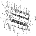
- a motor vehicle power commutation module 10 comprises a printed circuit board 12, eight power switches 14, 16, 18, 20, 22, 24, 26, 28, a first busbar 30 and a second busbar 32.
- an orthogonal reference system comprising a longitudinal axis L, a transverse axis T and a vertical axis V.
- the printed circuit board 12 has a planar rectangular shape.
- the printed circuit board 12 is positioned in a horizontal plane defined by the longitudinal axis L and the transverse axis T.
- the two opposite sides of greater length than the other two sides 38, 40 of the printed circuit board 12 define a first 34 and a second 36 longitudinal edge, respectively.
- the first busbar 30 and the second busbar 32 in the shape of a plate are positioned on either side of the two longitudinal edges 34, 36 of the printed circuit board 12.
- the two busbars 30, 32 are positioned next to the two longitudinal edges 34, 36, outside the surface of the printed circuit board 12, and also neither above, nor below the printed circuit board 12.
- the two busbars 30, 32 are generally in the shape of an 'L'.
- the two busbars 30, 32 comprise a longitudinal portion 42, 44 of rectangular shape, one straight edge 35, 37 of which extends longitudinally and parallel to the two longitudinal edges 34, 36 of the printed circuit board 12.
- the longitudinal portion 42, 44 is substantially the same length as the two longitudinal edges 34, 36 of the printed circuit board 12.
- the two busbars 30, 32 also comprise a second part 46, 48 of rectangular shape extending transversally along the same transverse side 38 of the printed circuit board 12.
- the two second parts 46, 48 have a transverse length that is identical to the other and are dimensioned such as to not be in contact with each other.
- the two busbars 30, 32 are positioned symmetrically with respect one another along a symmetry longitudinal axis S of the printed circuit board 12.
- the second parts of the busbars 46, 48 comprise a circular hole 50, 52 allowing the insertion of an electrical fixing means such as a terminal screwed to connect the power commutation module to the electrical distribution network of the vehicle.
- the two busbars 30, 32 are ideally arranged in the same horizontal plane as the printed circuit board 12, however the process for assembling the two busbars 30, 32 can only allow a placement of the busbars generally in the same horizontal plane as the printed circuit board 12.
- the eight power switches 14, 16, 18, 20, 22, 24, 26, 28 are grouped together in two series of four switches 14, 16, 18, 20.
- the power switches 14, 16, 18, 20, 22, 24, 26, 28 shown in Figure 1 are surface-mounted component- and D2Pack package-type power switches.
- a D2Pack package is a package of rectangular parallelepiped or cuboid shape comprising an upper face 54 and a lower face which are parallel and extend in the horizontal plane and are spaced apart by the four lateral faces 58, 60, 62, 64 of the rectangular parallelepiped.
- the lower face is provided with a connection metal base plate 66, and one of the lateral faces 64 is provided with a series of connection pins 68.
- connection pin series 68 comprises a pin called a control gate, several current input/output pins called a 'source' and finally a current input/output metal base plate 66 called a 'drain'.
- connection pins 68 of each series of switch 14, 16, 18, 20 are soldered on the upper face 13 of the printed circuit board 12 on a connection area 17.
- the connection pins 68 of a first series of switches 14, 16, 18, 20 extend transversally from each package lateral face 64 parallel to the vertical plane defined by the vertical axis V and the longitudinal axis L up to the area 17 for connecting the pins on the printed circuit board 12.
- the area 17 for connecting the pins 68 of the first series of switch 14, 16, 18, 20 extends longitudinally parallel to and at a short distance from a longitudinal edge 34 of the printed circuit board 12 such that each metal base plate 66, 67 can be mounted so as to be applied on a busbar 42 longitudinal portion arranged proximate and parallel to said longitudinal edge 34 of the printed circuit board 12.
- the base plates 67 of the first series of four switches 14, 16, 18, 20 are therefore mounted to be ideally aligned with each other on the busbar portion arranged longitudinally directly next to a longitudinal edge 34 of the printed circuit board 12.
- the process for assembling the four switches 14, 16, 18, 20 only allows a generally aligned positioning of the four switches 14, 16, 18, 20.
- the second series of four switches 22, 24, 26, 28 is mounted so as to be symmetrical with the first series 14, 16, 18, 20, along the symmetry longitudinal axis S of the printed circuit board 12.
- FIG. 2 shows the lower face 15 of the printed circuit board 12.
- the two busbars 30, 32 comprise means for fixing to the printed circuit board 12.
- the fixing means are tabs 72, 74, 76 consisting of a single piece with the busbars 30, 32.
- the tabs 72, 74, 76, of which there are three per busbar 30, 32, are soldered on the lower face 15 of the printed circuit board 12.
- the tabs 72, 74, 76 of each busbar 30, 32 are curved on the rims of the longitudinal edges 34, 36 of the printed circuit board 12.
- Each busbar 30, 32 comprises two tabs 72, 76 fixed at each end 78, 80 of the longitudinal edges 34, 36 of the printed circuit board 12, the third tab 74 being fixed approximately at equal distance from the other two tabs 72, 76.
- Each tab 72, 74, 76 comprises a curved part 82 surrounding the rims of the longitudinal edges 34, 36 of the printed circuit board 12 and a rectangular part 84, 86 soldered on the lower face 15 of the printed circuit 12.
- Each rectangular part 84 of the tabs 72, 76 fixed at each end 78, 80 of the longitudinal edges 34, 36 extends longitudinally from each transverse edge 38, 40 of the printed circuit board 12 towards the surface of the printed circuit board 12.
- Each rectangular part 84, 86 of the tabs 72, 74, 76 comprises transverse sides of same length whereas the longitudinal sides of the rectangular parts 84 of the tabs 72, 76 fixed at each end 78, 80 of the longitudinal edges 34, 36 are longer than the longitudinal sides of the rectangular parts 86 of the third tab 74. This difference is due to the need for reinforcing the rigidity of the commutation module at the ends of the printed circuit board.
- the busbars 30, 32 are thus held substantially in the same plane as the printed circuit board 12 by means of the busbars 30, 32 being held at the printed circuit board 12 by the fixing tabs 72, 74, 76, and via the power switches 14, 16, 18, 20, 22, 24, 26, 28, the pins 68 of which are soldered on the printed circuit board 12 and the metal base plates 66, 67 of which are soldered on the busbars 30, 32.
- the printed circuit board 12 comprises an electric signal connection area allowing the operation of the power commutation module 10.
- Two electric signals are control signals for the two switch 14, 16, 18, 20, 22, 24, 26, 28 series connected to the control gates of each series of switch 14, 16, 18, 20.
- the third signal is typically a strong current input electrically connected to the 'sources' of the two series of switches 14, 16, 18, 20, 22, 24, 26, 28.
- the two busbars 30, 32 are connected to the 'drains' of the two series of switches 14, 16, 18, 20, 22, 24, 26, 28, respectively.
- each series of switch 14, 16, 18, 20 can be controlled independently of each other in 'open switch' or 'closed switch' mode.
- the strong input current flows as far as the 'sources' of the controlled series of switches 14, 16, 18, 20, and, since the series of switches 14, 16, 18, 20 receives on the gates thereof a 'closed switch' command, the current passes through the switches of said series 14, 16, 18, 20 and therefore flows on the busbar 30 on which the drains or metal base plates 67 thereof are mounted.
- the two series of switches 14, 16, 18, 20, 22, 24, 26, 28 are controlled in 'open switch' mode, the strong input current becomes distributed through the two series of switches 14, 16, 18, 20, 22, 24, 26, 28 and is therefore distributed on the two busbars 30, 32.
- each series of four switches 14, 16, 18, 20 is an electrical assembly of four switches in parallel.
- the drains are connected together on the busbar 30, the sources are connected together on the printed circuit board 12 and the control gates are connected together on the printed circuit board 12.
- the two series of switches 14, 16, 18, 20, 22, 24, 26, 28 are connected together at a common source since the sources of the two series of switches 14, 16, 18, 20, 22, 24, 26, 28 are connected together.
- the arrangement of the commutation module 10 described above allows the constraints on the printed circuit board 12 to be reduced.
- the printed circuit board 12 only comprises components on a single face.
- the size of the printed circuit board 12 is reduced since the switch base plates 66, 67 are directly mounted on the busbars 30, 32, the busbars 30, 32 being arranged close to the outer periphery of the printed circuit board 12.
- the printed circuit board 12 does not have the constraint of heat dissipation of the power switches 14, 16, 18, 20, 22, 24, 26, 28 since the busbars 30, 32 conduct the strong current and allow for direct cooling of the package of each power switch 14, 16, 18, 20, 22, 24, 26, 28.
- the particularly advantageous layout of the busbars 30, 32 substantially in the same plane as the printed circuit board 12 allows for minimizing the height of the commutation module 10 and also allows for optimizing the constraints of heat dissipation and of fixing the commutation module 10.
- the symmetrical layout of the busbars 30, 32 and of the two series of power switches 14, 16, 18, 20, 22, 24, 26, 28 allows for minimizing the undesirable electrical effects of power commutation such as delays for commutating switches 14, 16, 18, 20, 22, 24, 26, 28 between the two series and bad distribution of current and therefore of heat in the two busbars 30, 32.
- the commutation module 10 can comprise only a single series of power switches 14, 16, 18, 20.
- the number of switches 14, 16, 18, 20 per series is not limited to four and can consequently be greater or less.
- the two busbars 30, 32 can not be substantially arranged in the same horizontal plane as the printed circuit board 12.
- the two busbars 30, 32 can be inclined along the vertical axis V independently of each other.
- the printed circuit board 12 and the two busbars 30, 32 can have various geometric shapes depending on the constraints for integrating the commutation module 10 into the vehicle.
- the means for fixing the busbar to the electrical distribution network of the vehicle can be different to that shown by Figure 1 .
Landscapes
- Engineering & Computer Science (AREA)
- Microelectronics & Electronic Packaging (AREA)
- Mechanical Engineering (AREA)
- Power Engineering (AREA)
- Rectifiers (AREA)
- Connection Or Junction Boxes (AREA)
- Inverter Devices (AREA)
- Structure Of Printed Boards (AREA)
- Combinations Of Printed Boards (AREA)
Abstract
Description
- The invention relates to a power commutation module, and more particularly to a specific arrangement of MOSFET power transistors on a printed circuit board.
- Power commutation modules for the electrical distribution of a vehicle in general comprise a printed circuit board provided with a power transistor and with busbars. It is known to solder the power transistors on the printed circuit board on one face and also to fix busbars on the printed circuit board. The busbars are generally fixed on the printed circuit face opposite the power transistors. The busbars are in contact with the power transistors by means of a plated-through hole, and thus allow the cooling of the power transistors. However, the printed circuit board has the constraint of having to be provided with power transistors which are generally bulky and drain strong currents. These constraints require a large printed circuit board surface not only for placing thereat the power transistors, in order to support the large currents passing therethrough, but also for supporting some of the heat dissipation required for the transistors.
- It is therefore important to propose a new solution solving these problems.
- A motor vehicle power commutation module comprises a printed circuit board, a first plate-shaped busbar, a first series of power switches each comprising a series of connection pins which are connected on the upper face of the printed circuit board and a metal base plate which is applied against the busbar. The first series of power switches is mounted on the first busbar, the power switches being generally aligned along a longitudinal edge of the first busbar. The longitudinal edge of the first busbar is arranged along a first longitudinal edge of the printed circuit board, and the portion of the first busbar on which the power switches are mounted is arranged next to the printed circuit board.
- Preferably, the busbar can be generally arranged in the same plane as the printed circuit board. The first busbar can comprise fixing tabs consisting of a single piece with the first busbar, the tabs extending from the straight edge of the busbar up to the lower face of the printed circuit board and being fixed on the lower face of the printed circuit board. A second series of power switches can be mounted on a second busbar, the second busbar and the second series of power switches being arranged in a similar manner to the first busbar and to the first series of switches, along another edge of the printed circuit board. The first and the second busbar can be arranged on either side of two opposite longitudinal edges of the printed circuit board, respectively. The power switches can be of the surface-mounted component type.
- Other features, aims and advantages of the invention will emerge upon reading the following detailed description, and with reference to the appended drawings, given by way of nonlimiting example and wherein:
-
Figure 1 is a schematic top view of the power commutation module according to the invention. -
Figure 2 is a schematic bottom view of the power commutation module according to the invention. - According to
Figure 1 , a motor vehiclepower commutation module 10 comprises a printedcircuit board 12, eightpower switches first busbar 30 and asecond busbar 32. In order to geometrically position the mentioned elements, there is defined, in a nonlimiting manner, an orthogonal reference system comprising a longitudinal axis L, a transverse axis T and a vertical axis V. - The printed
circuit board 12 has a planar rectangular shape. The printedcircuit board 12 is positioned in a horizontal plane defined by the longitudinal axis L and the transverse axis T. The two opposite sides of greater length than the other twosides 38, 40 of the printedcircuit board 12 define a first 34 and a second 36 longitudinal edge, respectively. - The
first busbar 30 and thesecond busbar 32 in the shape of a plate are positioned on either side of the twolongitudinal edges circuit board 12. In other words, the twobusbars longitudinal edges circuit board 12, and also neither above, nor below the printedcircuit board 12. The twobusbars busbars longitudinal portion straight edge longitudinal edges circuit board 12. Thelongitudinal portion longitudinal edges circuit board 12. The twobusbars second part circuit board 12. The twosecond parts busbars circuit board 12. The second parts of thebusbars circular hole busbars circuit board 12, however the process for assembling the twobusbars circuit board 12. - The eight
power switches switches Figure 1 are surface-mounted component- and D2Pack package-type power switches. - A D2Pack package is a package of rectangular parallelepiped or cuboid shape comprising an
upper face 54 and a lower face which are parallel and extend in the horizontal plane and are spaced apart by the fourlateral faces metal base plate 66, and one of thelateral faces 64 is provided with a series ofconnection pins 68. Typically, when thepower switch 14 is a power transistor of the insulated-gate field-effect transistor type, more commonly called a MOSFET, theconnection pin series 68 comprises a pin called a control gate, several current input/output pins called a 'source' and finally a current input/outputmetal base plate 66 called a 'drain'. - The
connection pins 68 of each series ofswitch upper face 13 of the printedcircuit board 12 on aconnection area 17. Theconnection pins 68 of a first series ofswitches lateral face 64 parallel to the vertical plane defined by the vertical axis V and the longitudinal axis L up to thearea 17 for connecting the pins on the printedcircuit board 12. Thearea 17 for connecting thepins 68 of the first series ofswitch longitudinal edge 34 of the printedcircuit board 12 such that eachmetal base plate busbar 42 longitudinal portion arranged proximate and parallel to saidlongitudinal edge 34 of the printedcircuit board 12. Thebase plates 67 of the first series of fourswitches longitudinal edge 34 of the printedcircuit board 12. However, the process for assembling the fourswitches switches switches first series circuit board 12. -
Figure 2 shows thelower face 15 of the printedcircuit board 12. The twobusbars circuit board 12. The fixing means aretabs busbars tabs busbar lower face 15 of the printedcircuit board 12. Thetabs busbar longitudinal edges circuit board 12. - Each
busbar tabs end longitudinal edges circuit board 12, thethird tab 74 being fixed approximately at equal distance from the other twotabs tab curved part 82 surrounding the rims of thelongitudinal edges printed circuit board 12 and arectangular part lower face 15 of the printedcircuit 12. Eachrectangular part 84 of thetabs end longitudinal edges transverse edge 38, 40 of the printedcircuit board 12 towards the surface of the printedcircuit board 12. - Each
rectangular part tabs rectangular parts 84 of thetabs end longitudinal edges rectangular parts 86 of thethird tab 74. This difference is due to the need for reinforcing the rigidity of the commutation module at the ends of the printed circuit board. - The
busbars circuit board 12 by means of thebusbars circuit board 12 by thefixing tabs power switches pins 68 of which are soldered on the printedcircuit board 12 and themetal base plates busbars - In an operational manner, the printed
circuit board 12 comprises an electric signal connection area allowing the operation of thepower commutation module 10. There are typically three electric signals. Two electric signals are control signals for the twoswitch switch switches - The two
busbars switches switch switches switches switches series busbar 30 on which the drains ormetal base plates 67 thereof are mounted. When the two series ofswitches switches busbars - It will be noted that each series of four
switches busbar 30, the sources are connected together on the printedcircuit board 12 and the control gates are connected together on the printedcircuit board 12. It will be noted that the two series ofswitches switches - The arrangement of the
commutation module 10 described above allows the constraints on the printedcircuit board 12 to be reduced. The printedcircuit board 12 only comprises components on a single face. The size of the printedcircuit board 12 is reduced since theswitch base plates busbars busbars circuit board 12. The printedcircuit board 12 does not have the constraint of heat dissipation of the power switches 14, 16, 18, 20, 22, 24, 26, 28 since thebusbars power switch - The particularly advantageous layout of the
busbars circuit board 12 allows for minimizing the height of thecommutation module 10 and also allows for optimizing the constraints of heat dissipation and of fixing thecommutation module 10. The symmetrical layout of thebusbars busbars - Alternatively, the
commutation module 10 can comprise only a single series of power switches 14, 16, 18, 20. The number ofswitches busbars circuit board 12. The twobusbars circuit board 12 and the twobusbars commutation module 10 into the vehicle. The means for fixing the busbar to the electrical distribution network of the vehicle can be different to that shown byFigure 1 .
Claims (6)
- Motor vehicle power commutation module (10) comprising:- a printed circuit board (12),- a first plate-shaped busbar (30),- a first series of power switches (14, 16, 18, 20) each comprising a series of connection pins (68) which are connected on the upper face (13) of the printed circuit board (12) and a metal base plate (67) which is applied against the busbar (30),characterized in that the first series of power switches (14, 16, 18, 20) is mounted on the first busbar (30), the power switches (14, 16, 18, 20) being generally aligned along a longitudinal edge (35) of the first busbar (30), in that said longitudinal edge (35) of the first busbar (30) is arranged along a first longitudinal edge (34) of the printed circuit board (12), and in that the portion (42) of the first busbar (30) on which the power switches (14, 16, 18, 20) are mounted is arranged next to the printed circuit board (12).
- Module (10) according to the preceding claim, characterized in that the busbar (30) is generally arranged in the same plane as the printed circuit board (12).
- Module (10) according to any one of the preceding claims, characterized in that the first busbar (30) comprises fixing tabs (72, 74, 76) consisting of a single piece with the first busbar (30), the tabs (72, 74, 76) extending from the straight edge (35) of the busbar (30) up to the lower face (15) of the printed circuit board (12), the tabs (72, 74, 76) being fixed on the lower face (15) of the printed circuit board (12).
- Module (10) according to any one of the preceding claims, characterized in that it comprises a second series of power switches (22, 24, 26, 28) which is mounted on a second busbar (32), the second busbar (32) and the second series of power switches (22, 24, 26, 28) being arranged in a similar manner to the first busbar (30) and to the first series of switches (14, 16, 18, 20), along another edge (36) of the printed circuit board (12).
- Module (10) according to Claim 4, characterized in that the first (30) and the second (32) busbar are arranged on either side of two opposite longitudinal edges (34, 36) of the printed circuit board (12), respectively.
- Module (10) according to any one of the preceding claims, characterized in that the power switches (14, 16, 18, 20, 22, 24, 26, 28) are of the surface-mounted component type.
Applications Claiming Priority (1)
| Application Number | Priority Date | Filing Date | Title |
|---|---|---|---|
| FR1654711A FR3052013B1 (en) | 2016-05-25 | 2016-05-25 | POWER SWITCHING MODULE |
Publications (2)
| Publication Number | Publication Date |
|---|---|
| EP3250011A1 true EP3250011A1 (en) | 2017-11-29 |
| EP3250011B1 EP3250011B1 (en) | 2023-09-27 |
Family
ID=56802610
Family Applications (1)
| Application Number | Title | Priority Date | Filing Date |
|---|---|---|---|
| EP17172298.6A Active EP3250011B1 (en) | 2016-05-25 | 2017-05-22 | Power commutation module |
Country Status (6)
| Country | Link |
|---|---|
| US (1) | US10177085B2 (en) |
| EP (1) | EP3250011B1 (en) |
| JP (1) | JP7010554B2 (en) |
| KR (1) | KR102432186B1 (en) |
| CN (1) | CN107454743B (en) |
| FR (1) | FR3052013B1 (en) |
Cited By (2)
| Publication number | Priority date | Publication date | Assignee | Title |
|---|---|---|---|---|
| EP3691103A1 (en) * | 2019-02-01 | 2020-08-05 | Aptiv Technologies Limited | Electric power module |
| DE102019130082B4 (en) | 2018-11-09 | 2021-12-02 | Sumitomo Wiring Systems, Ltd. | PCB arrangement |
Families Citing this family (3)
| Publication number | Priority date | Publication date | Assignee | Title |
|---|---|---|---|---|
| CN110337194B (en) * | 2019-07-25 | 2024-02-13 | 苏州华之杰电讯股份有限公司 | Connecting structure of parallel double MOS (Metal oxide semiconductor) tubes and PCBA (printed circuit board assembly) |
| CA3163239C (en) * | 2019-11-27 | 2025-05-13 | The Noco Company | Semiconductor device, printed circuit board (pcb), and method of interfacing control pin (gate pin) of a power semiconductor device (mosfet) to a printed circuit board (pcb) in a battery management system (bms) |
| EP4369872A1 (en) * | 2022-11-10 | 2024-05-15 | HS Elektronik Systeme GmbH | Solid state power switch assembly of an aircraft solid state power controller and method of providing a solid state power switch assembly for an aircraft solid state power controller |
Citations (3)
| Publication number | Priority date | Publication date | Assignee | Title |
|---|---|---|---|---|
| EP1100294A2 (en) * | 1999-11-09 | 2001-05-16 | Agile Systems Inc | Bus bar heat sink |
| CN203826375U (en) * | 2014-05-20 | 2014-09-10 | 北京海特远舟新能源科技有限公司 | Metal-Oxide-Semiconductor (MOS) tubes connected in parallel to realize a structure for controlling the opening and the closing of large current |
| WO2015104072A1 (en) * | 2014-01-13 | 2015-07-16 | Auto-Kabel Management Gmbh | Printed circuit board, circuit, and method for the production of a circuit |
Family Cites Families (5)
| Publication number | Priority date | Publication date | Assignee | Title |
|---|---|---|---|---|
| US6845017B2 (en) * | 2000-09-20 | 2005-01-18 | Ballard Power Systems Corporation | Substrate-level DC bus design to reduce module inductance |
| JP4162523B2 (en) * | 2002-06-03 | 2008-10-08 | シャープ株式会社 | Inverter |
| JP2004063681A (en) * | 2002-07-26 | 2004-02-26 | Hitachi Unisia Automotive Ltd | Semiconductor device |
| JP2010161089A (en) * | 2009-01-06 | 2010-07-22 | Calsonic Kansei Corp | Structure for mounting power element and heat sink |
| CN101834544B (en) * | 2010-04-27 | 2012-07-18 | 西安交通大学 | Synchronous rectifying circuit structure for high-frequency switch power supply |
-
2016
- 2016-05-25 FR FR1654711A patent/FR3052013B1/en active Active
-
2017
- 2017-05-22 EP EP17172298.6A patent/EP3250011B1/en active Active
- 2017-05-24 JP JP2017102383A patent/JP7010554B2/en active Active
- 2017-05-24 US US15/603,921 patent/US10177085B2/en active Active
- 2017-05-25 CN CN201710376221.2A patent/CN107454743B/en active Active
- 2017-05-25 KR KR1020170064535A patent/KR102432186B1/en active Active
Patent Citations (3)
| Publication number | Priority date | Publication date | Assignee | Title |
|---|---|---|---|---|
| EP1100294A2 (en) * | 1999-11-09 | 2001-05-16 | Agile Systems Inc | Bus bar heat sink |
| WO2015104072A1 (en) * | 2014-01-13 | 2015-07-16 | Auto-Kabel Management Gmbh | Printed circuit board, circuit, and method for the production of a circuit |
| CN203826375U (en) * | 2014-05-20 | 2014-09-10 | 北京海特远舟新能源科技有限公司 | Metal-Oxide-Semiconductor (MOS) tubes connected in parallel to realize a structure for controlling the opening and the closing of large current |
Cited By (2)
| Publication number | Priority date | Publication date | Assignee | Title |
|---|---|---|---|---|
| DE102019130082B4 (en) | 2018-11-09 | 2021-12-02 | Sumitomo Wiring Systems, Ltd. | PCB arrangement |
| EP3691103A1 (en) * | 2019-02-01 | 2020-08-05 | Aptiv Technologies Limited | Electric power module |
Also Published As
| Publication number | Publication date |
|---|---|
| KR20170133280A (en) | 2017-12-05 |
| FR3052013A1 (en) | 2017-12-01 |
| JP2017212446A (en) | 2017-11-30 |
| JP7010554B2 (en) | 2022-01-26 |
| US20170345749A1 (en) | 2017-11-30 |
| US10177085B2 (en) | 2019-01-08 |
| FR3052013B1 (en) | 2019-06-28 |
| EP3250011B1 (en) | 2023-09-27 |
| CN107454743A (en) | 2017-12-08 |
| CN107454743B (en) | 2019-11-22 |
| KR102432186B1 (en) | 2022-08-16 |
Similar Documents
| Publication | Publication Date | Title |
|---|---|---|
| US10177085B2 (en) | Power commutation module | |
| US10028400B2 (en) | Semiconductor device | |
| US10284105B2 (en) | Power converter | |
| JP2004319992A (en) | Module type power semiconductor module | |
| US20160352215A1 (en) | Power converter incorporated in case | |
| US20070165376A1 (en) | Three phase inverter power stage and assembly | |
| US6611066B2 (en) | Power distributor for vehicle | |
| JP5884775B2 (en) | Inverter device | |
| US20190082527A1 (en) | Circuit structure | |
| US6885097B2 (en) | Semiconductor device | |
| US10636740B2 (en) | Semiconductor device, method for manufacturing semiconductor device, and interface unit | |
| US5541453A (en) | Power semiconductor module | |
| CN104066311B (en) | Substrate gap retaining member and DC-to-AC converter | |
| US20160226367A1 (en) | High power electrical module and high power electrical circuit | |
| CN106898600A (en) | Semiconductor module | |
| JP2004063681A (en) | Semiconductor device | |
| US11343913B2 (en) | Circuit board structure | |
| JP2019102612A (en) | Interface unit and semiconductor device | |
| KR101019810B1 (en) | Switching device with two controlled phases | |
| JP7763716B2 (en) | Power Conversion Device | |
| JP7283243B2 (en) | power converter | |
| JP2023181374A (en) | power converter | |
| KR102603062B1 (en) | Input terminal of power module of double-side cooling | |
| WO2025203618A1 (en) | Semiconductor circuit breaker and board using semiconductor circuit breaker | |
| JP2021182793A (en) | Power unit and power converter |
Legal Events
| Date | Code | Title | Description |
|---|---|---|---|
| PUAI | Public reference made under article 153(3) epc to a published international application that has entered the european phase |
Free format text: ORIGINAL CODE: 0009012 |
|
| STAA | Information on the status of an ep patent application or granted ep patent |
Free format text: STATUS: THE APPLICATION HAS BEEN PUBLISHED |
|
| AK | Designated contracting states |
Kind code of ref document: A1 Designated state(s): AL AT BE BG CH CY CZ DE DK EE ES FI FR GB GR HR HU IE IS IT LI LT LU LV MC MK MT NL NO PL PT RO RS SE SI SK SM TR |
|
| AX | Request for extension of the european patent |
Extension state: BA ME |
|
| RIN1 | Information on inventor provided before grant (corrected) |
Inventor name: GUILLANTON, ERWAN Inventor name: PEROT, AYMERIC |
|
| STAA | Information on the status of an ep patent application or granted ep patent |
Free format text: STATUS: REQUEST FOR EXAMINATION WAS MADE |
|
| 17P | Request for examination filed |
Effective date: 20180529 |
|
| RBV | Designated contracting states (corrected) |
Designated state(s): AL AT BE BG CH CY CZ DE DK EE ES FI FR GB GR HR HU IE IS IT LI LT LU LV MC MK MT NL NO PL PT RO RS SE SI SK SM TR |
|
| RAP1 | Party data changed (applicant data changed or rights of an application transferred) |
Owner name: APTIV TECHNOLOGIES LIMITED |
|
| STAA | Information on the status of an ep patent application or granted ep patent |
Free format text: STATUS: EXAMINATION IS IN PROGRESS |
|
| 17Q | First examination report despatched |
Effective date: 20210111 |
|
| RAP3 | Party data changed (applicant data changed or rights of an application transferred) |
Owner name: APTIV TECHNOLOGIES LIMITED |
|
| GRAP | Despatch of communication of intention to grant a patent |
Free format text: ORIGINAL CODE: EPIDOSNIGR1 |
|
| STAA | Information on the status of an ep patent application or granted ep patent |
Free format text: STATUS: GRANT OF PATENT IS INTENDED |
|
| RIC1 | Information provided on ipc code assigned before grant |
Ipc: H05K 7/14 20060101ALI20230324BHEP Ipc: H05K 1/02 20060101AFI20230324BHEP |
|
| INTG | Intention to grant announced |
Effective date: 20230420 |
|
| GRAS | Grant fee paid |
Free format text: ORIGINAL CODE: EPIDOSNIGR3 |
|
| GRAA | (expected) grant |
Free format text: ORIGINAL CODE: 0009210 |
|
| STAA | Information on the status of an ep patent application or granted ep patent |
Free format text: STATUS: THE PATENT HAS BEEN GRANTED |
|
| P01 | Opt-out of the competence of the unified patent court (upc) registered |
Effective date: 20230728 |
|
| AK | Designated contracting states |
Kind code of ref document: B1 Designated state(s): AL AT BE BG CH CY CZ DE DK EE ES FI FR GB GR HR HU IE IS IT LI LT LU LV MC MK MT NL NO PL PT RO RS SE SI SK SM TR |
|
| REG | Reference to a national code |
Ref country code: GB Ref legal event code: FG4D |
|
| REG | Reference to a national code |
Ref country code: CH Ref legal event code: EP |
|
| REG | Reference to a national code |
Ref country code: DE Ref legal event code: R096 Ref document number: 602017074589 Country of ref document: DE |
|
| REG | Reference to a national code |
Ref country code: IE Ref legal event code: FG4D |
|
| REG | Reference to a national code |
Ref country code: LT Ref legal event code: MG9D |
|
| PG25 | Lapsed in a contracting state [announced via postgrant information from national office to epo] |
Ref country code: GR Free format text: LAPSE BECAUSE OF FAILURE TO SUBMIT A TRANSLATION OF THE DESCRIPTION OR TO PAY THE FEE WITHIN THE PRESCRIBED TIME-LIMIT Effective date: 20231228 |
|
| PG25 | Lapsed in a contracting state [announced via postgrant information from national office to epo] |
Ref country code: SE Free format text: LAPSE BECAUSE OF FAILURE TO SUBMIT A TRANSLATION OF THE DESCRIPTION OR TO PAY THE FEE WITHIN THE PRESCRIBED TIME-LIMIT Effective date: 20230927 Ref country code: RS Free format text: LAPSE BECAUSE OF FAILURE TO SUBMIT A TRANSLATION OF THE DESCRIPTION OR TO PAY THE FEE WITHIN THE PRESCRIBED TIME-LIMIT Effective date: 20230927 Ref country code: NO Free format text: LAPSE BECAUSE OF FAILURE TO SUBMIT A TRANSLATION OF THE DESCRIPTION OR TO PAY THE FEE WITHIN THE PRESCRIBED TIME-LIMIT Effective date: 20231227 Ref country code: LV Free format text: LAPSE BECAUSE OF FAILURE TO SUBMIT A TRANSLATION OF THE DESCRIPTION OR TO PAY THE FEE WITHIN THE PRESCRIBED TIME-LIMIT Effective date: 20230927 Ref country code: LT Free format text: LAPSE BECAUSE OF FAILURE TO SUBMIT A TRANSLATION OF THE DESCRIPTION OR TO PAY THE FEE WITHIN THE PRESCRIBED TIME-LIMIT Effective date: 20230927 Ref country code: HR Free format text: LAPSE BECAUSE OF FAILURE TO SUBMIT A TRANSLATION OF THE DESCRIPTION OR TO PAY THE FEE WITHIN THE PRESCRIBED TIME-LIMIT Effective date: 20230927 Ref country code: GR Free format text: LAPSE BECAUSE OF FAILURE TO SUBMIT A TRANSLATION OF THE DESCRIPTION OR TO PAY THE FEE WITHIN THE PRESCRIBED TIME-LIMIT Effective date: 20231228 Ref country code: FI Free format text: LAPSE BECAUSE OF FAILURE TO SUBMIT A TRANSLATION OF THE DESCRIPTION OR TO PAY THE FEE WITHIN THE PRESCRIBED TIME-LIMIT Effective date: 20230927 |
|
| REG | Reference to a national code |
Ref country code: NL Ref legal event code: MP Effective date: 20230927 |
|
| REG | Reference to a national code |
Ref country code: AT Ref legal event code: MK05 Ref document number: 1616668 Country of ref document: AT Kind code of ref document: T Effective date: 20230927 |
|
| PG25 | Lapsed in a contracting state [announced via postgrant information from national office to epo] |
Ref country code: NL Free format text: LAPSE BECAUSE OF FAILURE TO SUBMIT A TRANSLATION OF THE DESCRIPTION OR TO PAY THE FEE WITHIN THE PRESCRIBED TIME-LIMIT Effective date: 20230927 |
|
| PG25 | Lapsed in a contracting state [announced via postgrant information from national office to epo] |
Ref country code: IS Free format text: LAPSE BECAUSE OF FAILURE TO SUBMIT A TRANSLATION OF THE DESCRIPTION OR TO PAY THE FEE WITHIN THE PRESCRIBED TIME-LIMIT Effective date: 20240127 |
|
| PG25 | Lapsed in a contracting state [announced via postgrant information from national office to epo] |
Ref country code: AT Free format text: LAPSE BECAUSE OF FAILURE TO SUBMIT A TRANSLATION OF THE DESCRIPTION OR TO PAY THE FEE WITHIN THE PRESCRIBED TIME-LIMIT Effective date: 20230927 |
|
| PG25 | Lapsed in a contracting state [announced via postgrant information from national office to epo] |
Ref country code: ES Free format text: LAPSE BECAUSE OF FAILURE TO SUBMIT A TRANSLATION OF THE DESCRIPTION OR TO PAY THE FEE WITHIN THE PRESCRIBED TIME-LIMIT Effective date: 20230927 |
|
| PG25 | Lapsed in a contracting state [announced via postgrant information from national office to epo] |
Ref country code: SM Free format text: LAPSE BECAUSE OF FAILURE TO SUBMIT A TRANSLATION OF THE DESCRIPTION OR TO PAY THE FEE WITHIN THE PRESCRIBED TIME-LIMIT Effective date: 20230927 Ref country code: RO Free format text: LAPSE BECAUSE OF FAILURE TO SUBMIT A TRANSLATION OF THE DESCRIPTION OR TO PAY THE FEE WITHIN THE PRESCRIBED TIME-LIMIT Effective date: 20230927 Ref country code: IS Free format text: LAPSE BECAUSE OF FAILURE TO SUBMIT A TRANSLATION OF THE DESCRIPTION OR TO PAY THE FEE WITHIN THE PRESCRIBED TIME-LIMIT Effective date: 20240127 Ref country code: ES Free format text: LAPSE BECAUSE OF FAILURE TO SUBMIT A TRANSLATION OF THE DESCRIPTION OR TO PAY THE FEE WITHIN THE PRESCRIBED TIME-LIMIT Effective date: 20230927 Ref country code: EE Free format text: LAPSE BECAUSE OF FAILURE TO SUBMIT A TRANSLATION OF THE DESCRIPTION OR TO PAY THE FEE WITHIN THE PRESCRIBED TIME-LIMIT Effective date: 20230927 Ref country code: CZ Free format text: LAPSE BECAUSE OF FAILURE TO SUBMIT A TRANSLATION OF THE DESCRIPTION OR TO PAY THE FEE WITHIN THE PRESCRIBED TIME-LIMIT Effective date: 20230927 Ref country code: AT Free format text: LAPSE BECAUSE OF FAILURE TO SUBMIT A TRANSLATION OF THE DESCRIPTION OR TO PAY THE FEE WITHIN THE PRESCRIBED TIME-LIMIT Effective date: 20230927 Ref country code: PT Free format text: LAPSE BECAUSE OF FAILURE TO SUBMIT A TRANSLATION OF THE DESCRIPTION OR TO PAY THE FEE WITHIN THE PRESCRIBED TIME-LIMIT Effective date: 20240129 Ref country code: SK Free format text: LAPSE BECAUSE OF FAILURE TO SUBMIT A TRANSLATION OF THE DESCRIPTION OR TO PAY THE FEE WITHIN THE PRESCRIBED TIME-LIMIT Effective date: 20230927 |
|
| PG25 | Lapsed in a contracting state [announced via postgrant information from national office to epo] |
Ref country code: PL Free format text: LAPSE BECAUSE OF FAILURE TO SUBMIT A TRANSLATION OF THE DESCRIPTION OR TO PAY THE FEE WITHIN THE PRESCRIBED TIME-LIMIT Effective date: 20230927 Ref country code: IT Free format text: LAPSE BECAUSE OF FAILURE TO SUBMIT A TRANSLATION OF THE DESCRIPTION OR TO PAY THE FEE WITHIN THE PRESCRIBED TIME-LIMIT Effective date: 20230927 |
|
| REG | Reference to a national code |
Ref country code: DE Ref legal event code: R097 Ref document number: 602017074589 Country of ref document: DE |
|
| PG25 | Lapsed in a contracting state [announced via postgrant information from national office to epo] |
Ref country code: DK Free format text: LAPSE BECAUSE OF FAILURE TO SUBMIT A TRANSLATION OF THE DESCRIPTION OR TO PAY THE FEE WITHIN THE PRESCRIBED TIME-LIMIT Effective date: 20230927 |
|
| PG25 | Lapsed in a contracting state [announced via postgrant information from national office to epo] |
Ref country code: DK Free format text: LAPSE BECAUSE OF FAILURE TO SUBMIT A TRANSLATION OF THE DESCRIPTION OR TO PAY THE FEE WITHIN THE PRESCRIBED TIME-LIMIT Effective date: 20230927 |
|
| PLBE | No opposition filed within time limit |
Free format text: ORIGINAL CODE: 0009261 |
|
| STAA | Information on the status of an ep patent application or granted ep patent |
Free format text: STATUS: NO OPPOSITION FILED WITHIN TIME LIMIT |
|
| 26N | No opposition filed |
Effective date: 20240628 |
|
| PG25 | Lapsed in a contracting state [announced via postgrant information from national office to epo] |
Ref country code: SI Free format text: LAPSE BECAUSE OF FAILURE TO SUBMIT A TRANSLATION OF THE DESCRIPTION OR TO PAY THE FEE WITHIN THE PRESCRIBED TIME-LIMIT Effective date: 20230927 |
|
| PG25 | Lapsed in a contracting state [announced via postgrant information from national office to epo] |
Ref country code: SI Free format text: LAPSE BECAUSE OF FAILURE TO SUBMIT A TRANSLATION OF THE DESCRIPTION OR TO PAY THE FEE WITHIN THE PRESCRIBED TIME-LIMIT Effective date: 20230927 |
|
| PG25 | Lapsed in a contracting state [announced via postgrant information from national office to epo] |
Ref country code: BG Free format text: LAPSE BECAUSE OF FAILURE TO SUBMIT A TRANSLATION OF THE DESCRIPTION OR TO PAY THE FEE WITHIN THE PRESCRIBED TIME-LIMIT Effective date: 20230927 |
|
| PG25 | Lapsed in a contracting state [announced via postgrant information from national office to epo] |
Ref country code: BG Free format text: LAPSE BECAUSE OF FAILURE TO SUBMIT A TRANSLATION OF THE DESCRIPTION OR TO PAY THE FEE WITHIN THE PRESCRIBED TIME-LIMIT Effective date: 20230927 |
|
| REG | Reference to a national code |
Ref country code: CH Ref legal event code: PL |
|
| PG25 | Lapsed in a contracting state [announced via postgrant information from national office to epo] |
Ref country code: MC Free format text: LAPSE BECAUSE OF FAILURE TO SUBMIT A TRANSLATION OF THE DESCRIPTION OR TO PAY THE FEE WITHIN THE PRESCRIBED TIME-LIMIT Effective date: 20230927 |
|
| PG25 | Lapsed in a contracting state [announced via postgrant information from national office to epo] |
Ref country code: LU Free format text: LAPSE BECAUSE OF NON-PAYMENT OF DUE FEES Effective date: 20240522 |
|
| PG25 | Lapsed in a contracting state [announced via postgrant information from national office to epo] |
Ref country code: MC Free format text: LAPSE BECAUSE OF FAILURE TO SUBMIT A TRANSLATION OF THE DESCRIPTION OR TO PAY THE FEE WITHIN THE PRESCRIBED TIME-LIMIT Effective date: 20230927 Ref country code: LU Free format text: LAPSE BECAUSE OF NON-PAYMENT OF DUE FEES Effective date: 20240522 Ref country code: CH Free format text: LAPSE BECAUSE OF NON-PAYMENT OF DUE FEES Effective date: 20240531 |
|
| REG | Reference to a national code |
Ref country code: BE Ref legal event code: MM Effective date: 20240531 |
|
| PG25 | Lapsed in a contracting state [announced via postgrant information from national office to epo] |
Ref country code: IE Free format text: LAPSE BECAUSE OF NON-PAYMENT OF DUE FEES Effective date: 20240522 |
|
| PG25 | Lapsed in a contracting state [announced via postgrant information from national office to epo] |
Ref country code: BE Free format text: LAPSE BECAUSE OF NON-PAYMENT OF DUE FEES Effective date: 20240531 |
|
| REG | Reference to a national code |
Ref country code: DE Ref legal event code: R081 Ref document number: 602017074589 Country of ref document: DE Owner name: APTIV TECHNOLOGIES AG, CH Free format text: FORMER OWNER: APTIV TECHNOLOGIES LIMITED, ST. MICHAEL, BB |
|
| PGFP | Annual fee paid to national office [announced via postgrant information from national office to epo] |
Ref country code: DE Payment date: 20250422 Year of fee payment: 9 |
|
| PGFP | Annual fee paid to national office [announced via postgrant information from national office to epo] |
Ref country code: FR Payment date: 20250513 Year of fee payment: 9 |
|
| PG25 | Lapsed in a contracting state [announced via postgrant information from national office to epo] |
Ref country code: CY Free format text: LAPSE BECAUSE OF FAILURE TO SUBMIT A TRANSLATION OF THE DESCRIPTION OR TO PAY THE FEE WITHIN THE PRESCRIBED TIME-LIMIT; INVALID AB INITIO Effective date: 20170522 |
|
| PG25 | Lapsed in a contracting state [announced via postgrant information from national office to epo] |
Ref country code: HU Free format text: LAPSE BECAUSE OF FAILURE TO SUBMIT A TRANSLATION OF THE DESCRIPTION OR TO PAY THE FEE WITHIN THE PRESCRIBED TIME-LIMIT; INVALID AB INITIO Effective date: 20170522 |
|
| PGFP | Annual fee paid to national office [announced via postgrant information from national office to epo] |
Ref country code: GB Payment date: 20260313 Year of fee payment: 10 |