EP3249749A1 - Antenna device with accurate beam elevation control useable on an automated vehicle - Google Patents
Antenna device with accurate beam elevation control useable on an automated vehicle Download PDFInfo
- Publication number
- EP3249749A1 EP3249749A1 EP17172670.6A EP17172670A EP3249749A1 EP 3249749 A1 EP3249749 A1 EP 3249749A1 EP 17172670 A EP17172670 A EP 17172670A EP 3249749 A1 EP3249749 A1 EP 3249749A1
- Authority
- EP
- European Patent Office
- Prior art keywords
- conductive
- conductive pads
- slot
- pads
- antenna device
- Prior art date
- Legal status (The legal status is an assumption and is not a legal conclusion. Google has not performed a legal analysis and makes no representation as to the accuracy of the status listed.)
- Granted
Links
Images

Classifications
-
- H—ELECTRICITY
- H01—ELECTRIC ELEMENTS
- H01Q—ANTENNAS, i.e. RADIO AERIALS
- H01Q1/00—Details of, or arrangements associated with, antennas
- H01Q1/27—Adaptation for use in or on movable bodies
- H01Q1/32—Adaptation for use in or on road or rail vehicles
-
- H—ELECTRICITY
- H01—ELECTRIC ELEMENTS
- H01Q—ANTENNAS, i.e. RADIO AERIALS
- H01Q1/00—Details of, or arrangements associated with, antennas
- H01Q1/27—Adaptation for use in or on movable bodies
- H01Q1/32—Adaptation for use in or on road or rail vehicles
- H01Q1/3208—Adaptation for use in or on road or rail vehicles characterised by the application wherein the antenna is used
- H01Q1/3233—Adaptation for use in or on road or rail vehicles characterised by the application wherein the antenna is used particular used as part of a sensor or in a security system, e.g. for automotive radar, navigation systems
-
- G—PHYSICS
- G01—MEASURING; TESTING
- G01S—RADIO DIRECTION-FINDING; RADIO NAVIGATION; DETERMINING DISTANCE OR VELOCITY BY USE OF RADIO WAVES; LOCATING OR PRESENCE-DETECTING BY USE OF THE REFLECTION OR RERADIATION OF RADIO WAVES; ANALOGOUS ARRANGEMENTS USING OTHER WAVES
- G01S13/00—Systems using the reflection or reradiation of radio waves, e.g. radar systems; Analogous systems using reflection or reradiation of waves whose nature or wavelength is irrelevant or unspecified
- G01S13/88—Radar or analogous systems specially adapted for specific applications
- G01S13/93—Radar or analogous systems specially adapted for specific applications for anti-collision purposes
- G01S13/931—Radar or analogous systems specially adapted for specific applications for anti-collision purposes of land vehicles
-
- H—ELECTRICITY
- H01—ELECTRIC ELEMENTS
- H01Q—ANTENNAS, i.e. RADIO AERIALS
- H01Q1/00—Details of, or arrangements associated with, antennas
- H01Q1/27—Adaptation for use in or on movable bodies
- H01Q1/32—Adaptation for use in or on road or rail vehicles
- H01Q1/325—Adaptation for use in or on road or rail vehicles characterised by the location of the antenna on the vehicle
- H01Q1/3283—Adaptation for use in or on road or rail vehicles characterised by the location of the antenna on the vehicle side-mounted antennas, e.g. bumper-mounted, door-mounted
-
- H—ELECTRICITY
- H01—ELECTRIC ELEMENTS
- H01Q—ANTENNAS, i.e. RADIO AERIALS
- H01Q21/00—Antenna arrays or systems
- H01Q21/0006—Particular feeding systems
- H01Q21/0037—Particular feeding systems linear waveguide fed arrays
- H01Q21/0043—Slotted waveguides
-
- H—ELECTRICITY
- H01—ELECTRIC ELEMENTS
- H01Q—ANTENNAS, i.e. RADIO AERIALS
- H01Q21/00—Antenna arrays or systems
- H01Q21/06—Arrays of individually energised antenna units similarly polarised and spaced apart
- H01Q21/061—Two dimensional planar arrays
- H01Q21/065—Patch antenna array
-
- H—ELECTRICITY
- H01—ELECTRIC ELEMENTS
- H01Q—ANTENNAS, i.e. RADIO AERIALS
- H01Q21/00—Antenna arrays or systems
- H01Q21/06—Arrays of individually energised antenna units similarly polarised and spaced apart
- H01Q21/08—Arrays of individually energised antenna units similarly polarised and spaced apart the units being spaced along or adjacent to a rectilinear path
-
- H—ELECTRICITY
- H01—ELECTRIC ELEMENTS
- H01Q—ANTENNAS, i.e. RADIO AERIALS
- H01Q3/00—Arrangements for changing or varying the orientation or the shape of the directional pattern of the waves radiated from an antenna or antenna system
- H01Q3/24—Arrangements for changing or varying the orientation or the shape of the directional pattern of the waves radiated from an antenna or antenna system varying the orientation by switching energy from one active radiating element to another, e.g. for beam switching
-
- G—PHYSICS
- G01—MEASURING; TESTING
- G01S—RADIO DIRECTION-FINDING; RADIO NAVIGATION; DETERMINING DISTANCE OR VELOCITY BY USE OF RADIO WAVES; LOCATING OR PRESENCE-DETECTING BY USE OF THE REFLECTION OR RERADIATION OF RADIO WAVES; ANALOGOUS ARRANGEMENTS USING OTHER WAVES
- G01S13/00—Systems using the reflection or reradiation of radio waves, e.g. radar systems; Analogous systems using reflection or reradiation of waves whose nature or wavelength is irrelevant or unspecified
- G01S13/88—Radar or analogous systems specially adapted for specific applications
- G01S13/93—Radar or analogous systems specially adapted for specific applications for anti-collision purposes
- G01S13/931—Radar or analogous systems specially adapted for specific applications for anti-collision purposes of land vehicles
- G01S2013/9327—Sensor installation details
- G01S2013/93271—Sensor installation details in the front of the vehicles
Definitions
- Radar and other detection systems have a variety of uses. More recently, automotive vehicles have included increasing amounts of detection technology that utilizes radar signaling or principles for detecting objects in the vicinity or pathway of a vehicle.
- the inaccuracy of the beam elevation results from the way in which the antenna portion has been built or manufactured.
- the size of an antenna device desired for use on an automotive vehicle is so small that minor manufacturing discrepancies can result in pronounced beam elevation error. Improvements in antenna design and manufacturing techniques are needed to avoid inaccuracies in detector performance and scrap parts resulting from inaccuracies during manufacturing.
- An illustrative example antenna device includes a substrate having a first surface and a second surface. A plurality of conductive pads are on the first surface. A first conductive strip extends from a first one of the conductive pads toward an adjacent, second one of the conductive pads. The first conductive strip is spaced from the second one of the conductive pads. Second and third conductive strips extend between the first one of the conductive pads and the second one of the conductive pads. The second and third conductive strips establish a conductive connection between the first one of the conductive pads and the second one of the conductive pads. The second and third conductive strips are respectively on opposite sides of the first conductive strip. A slot in the second surface of the substrate is aligned with at least a portion of the first conductive strip.
- the plurality of conductive pads includes a first array of conductive pads aligned with the first one of the conductive pads on a side of the first one of the conductive pads that is opposite the second one of the conductive pads.
- the first array of conductive pads are conductively coupled in series.
- the plurality of conductive pads includes a second array of conductive pads aligned with the second one of the conductive pads on a side of the second one of the conductive pads that is opposite the first one of the conductive pads.
- the second array of conductive pads are conductively coupled in series.
- energy transmitted through the slot is conducted by the first conductive strip
- the first array of conductive pads are configured to radiate based on energy received by the first one of the conductive pads from the first conductive strip
- the second array of conductive pads are configured to radiate based on energy received by the second one of the conductive pads from at least one of the second and third conductive strips.
- the plurality of conductive pads are arranged in a line and a spacing between adjacent ones of the conductive pads is equal to a wavelength of radiation from the antenna device at a selected frequency.
- the slot has a slot width and a slot length, the slot length is oriented transverse to a direction from the first one of the conductive pads toward the second one of the conductive pads, and the slot length is less than a spacing between the second and third conductive strips.
- the slot is U-shaped.
- energy transmitted through the slot is directly incident upon the first conductive strip, the first conductive strip conducts energy to the first one of the conductive pads, and the second and third conductive strips conduct energy from the first one of the conductive pads to the second one of the conductive pads.
- the first conductive strip has a first portion oriented in a direction from the first one of the conductive pads toward the second one of the conductive pads and the first conductive strip has a second portion oriented transverse to the first portion.
- An example embodiment having one or more features of the antenna device of any of the previous paragraphs includes a substrate integrated waveguide situated near the second surface of the substrate.
- the substrate integrated waveguide is situated to direct energy toward the slot.
- An illustrative example method of making an antenna device includes establishing a plurality of conductive pads on a first surface of a substrate; establishing a first conductive strip extending from a first one of the conductive pads toward an adjacent, second one of the conductive pads, the first conductive strip being spaced from the second one of the conductive pads; establishing second and third conductive strips extending between the first one of the conductive pads and the second one of the conductive pads, the second and third conductive strips establishing a conductive connection between the first one of the conductive pads and the second one of the conductive pads, the second and third conductive strips respectively being on opposite sides of the first conductive strip; and forming a slot in a second surface of the substrate, the slot being aligned with at least a portion of the first conductive strip.
- establishing the plurality of conductive pads includes establishing a first array of conductive pads aligned with the first one of the conductive pads on a side of the first one of the conductive pads that is opposite the second one of the conductive pads; conductively coupling the first array of conductive pads in series; establishing a second array of conductive pads aligned with a second one of the conductive pads on a side of the second one of the conductive pads that is opposite the first one of the conductive pads; and conductively coupling the second array of conductive pads in series.
- establishing the plurality of conductive pads includes arranging the plurality of conductive pads in a line and spacing adjacent ones of the conductive pads from each other a distance equal to a wavelength of radiation from the antenna device at a selected frequency.
- forming the slot includes establishing a slot width and a slot length, orienting the slot length transverse to a direction from the first one of the conductive pads toward the second one of the conductive pads, and establishing the slot length to be less than a spacing between the second and third conductive strips.
- establishing the first conductive strip includes orienting a first portion of the first conductive strip in a direction from the first one of the conductive pads toward the second one of the conductive pads and orienting a second portion of the first conductive strip transverse to the first portion.
- An example embodiment having one or more features of the method of any of the previous paragraphs includes situating a substrate integrated waveguide near the second surface of the substrate where the substrate integrated waveguide is configured to direct energy toward the slot.
- An illustrative example embodiment of a detector for use on a vehicle for detecting an object in a vicinity or pathway of the vehicle includes an antenna device configured to emit radiation in a selected beam pattern at a selected angle relative to an associated vehicle.
- the antenna device includes a substrate having a first surface and a second surface; a plurality of conductive pads on the first surface, the plurality of conductive pads including a first array of conductive pads conductively coupled in series and a second array of conductive pads conductively coupled in series; a first conductive strip extending from a first one of the conductive pads of the first array toward an adjacent, second one of the conductive pads of the second array, the first conductive strip is spaced from the second one of the conductive pads; second and third conductive strips extending between the first one of the conductive pads and the second one of the conductive pads, the second and third conductive strips establishing a conductive connection between the first one of the conductive pads and the second one of the conductive pads, the second and third conductive strips respectively being on
- energy transmitted through the slot is conducted by the first conductive strip; the first array of conductive pads are configured to radiate based on energy received by the first one of the conductive paths from the first conductive strip; the second array of conductive paths are configured to radiate based on energy received by the second one of the conductive pads from at least one of the second and third conductive strips; and the at least one of the second and third conductive strips receives energy from the first one of the conductive pads.
- energy transmitted through the slot is directly incident upon the first conductive strip; the first conductive strip conducts energy to the first one of the conductive pads; and the second and third conductive strips conduct energy from the first one of the conductive pads to the second one of the conductive pads.
- An example embodiment having one or more features of the detector of any of the previous paragraphs includes a substrate integrated waveguide situated near the second surface of the substrate.
- the substrate integrated waveguide is situated to direct energy toward the slot.
- Embodiments of this invention provide control over the orientation of a beam radiated by an antenna device.
- One example use for antenna devices having features of the disclosed example embodiment is to provide a narrow elevation, wide azimuth beam pattern. Such beams are useful, for example, in radar or other detector systems, which may be useful for automotive vehicles including automated vehicles.
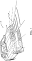
- Figure 1 schematically illustrates an example vehicle 20 that has a detector 22 supported on the vehicle.
- the detector 22 includes an antenna device that radiates a beam 24 in a selected direction and at a selected orientation relative to the vehicle 20.
- the example radiated beam 24 is a narrow elevation, wide azimuth beam, which has a relatively compact height in the vertical direction and a relatively wide spread in the horizontal direction. Such beams are useful for detecting objects in a pathway of the vehicle 20 for various purposes.
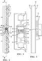
- Figures 2-4 schematically show selected features of an example antenna device that is part of the detector 22.
- the antenna device includes a substrate 30 having a first surface 32 and a second surface 34.
- the first surface 32 corresponds to a conductive plane while the second surface 34 corresponds to a ground plane in some example embodiments.
- the material of the substrate 30 may be selected to achieve desired loss, bandwidth, and cost characteristics.
- One example embodiment includes the commercially available material known as Rodgers 4350B.
- Other embodiments include materials, such as polytetrafluoroethylene, which may be more expensive but tends to introduce less loss. Given this description, those skilled in the art will be able to select an appropriate material to meet their particular needs.
- a slot 36 is formed in the second surface 34 of the substrate 30.
- the total area or length of the slot 36 controls the efficiency of energy transmission.
- the slot 36 may have a variety of configurations to achieve the desired efficiency and still fit within the available space. As best appreciated from Figure 3 , the slot 36 has a U-shaped configuration.
- the antenna device includes a plurality of conductive pads 40 arranged in a line on the first surface 32 of the substrate 30.
- the plurality of conductive pads 40 includes a first array of conductive pads at 42 and a second array of conductive pads at 44. All of the plurality of conductive pads 40 may be considered a single array.
- the first array 42 and second array 44 are utilized for discussion purposes.
- the plurality of conductive pads 40 may be established on the surface 32 using known etching techniques, for example.
- the first array 42 includes a first one of the conductive pads 46. Other conductive pads of the first array 42 are connected in series with the first one of the conductive pads 46. The other conductive pads of the first array 42 are conductively connected by conductive strips 48, which in this embodiment comprise micro-strips.
- the second array 44 includes a second one of the conductive pads 50. Others of the conductive pads within the second array 44 are conductively coupled in series with the second one of the conductive pads 50. Conductive strips 54, such as micro-strips, conductively couple the conductive pads of the second array 44 to each other in series.
- the spacing between the conductive pads 40 in an example embodiment corresponds to one wavelength for a selected frequency of radiation from the antenna device.
- the slot 36 is aligned with the spacing between the first one of the conductive pads 46 and the second one of the conductive pads 50.
- a first conductive strip 60 extends from the first one of the conductive pads 46 toward the second one of the conductive pads 50 without making electrically conductive contact with the second one of the conductive pads 50.
- the total length of the first conductive strip 60 determines the efficiency of energy transmission.
- the first conductive strip is more than a single, straight line.
- the first conductive strip 60 has a first portion 62 that is oriented parallel to a direction from the first one of the conductive pads 46 toward the second one of the conductive pads 50.
- a second portion 64 of the first conductive strip 60 is oriented transverse to the first portion 62.
- the first conductive strip 60 is T-shaped in this example.
- a second conductive strip 66 conductively couples the first one of the conductive pads 46 to the second one of the conductive pads 50.
- a third conductive strip 68 also couples the first one of the conductive pads 46 to the second one of the conductive pads 50.
- the second conductive strip 66 and third conductive strip 68, respectively, are on opposite sides of the first conductive strip 60.
- the first array 42 including the first one of the conductive pads 46 and the second array 44 including the second one of the conductive pads 50 are symmetrically arranged with respect to the location of the slot 36 and the conductive strips 60, 66 and 68. As illustrated, equal numbers of conductive pads 40 are on opposite sides of that location.
- the pads in the first array 42 also have the same configuration as those in the second array 44. In such embodiments, the first array 42 is a mirror image of the second array 44 when considered exclusive of the conductive strips 60, 66 and 68.
- Such symmetry and the relationship between the slot 36 and the first conductive strip 60 ensures a desired beam angle even if the position of the slot 36 relative to the first one of the conductive pads 46 varies slightly while still having the slot 36 aligned with at least a portion of the first conductive strip 60.
- the conductive pads 40 and all conductive strips connecting them including the first conductive strip 60, second conductive strip 66 and third conductive strip 68 are all etched as one piece on the first surface 32.
- the slot 36 has a slot length and a slot width.
- the slot length is transverse to each of the first portion 62 of the first conductive strip 60, the second conductive strip 66, and the third conductive strip 68.
- the slot length is less than a distance or spacing between the second conductive strip 66 and the third conductive strip 68.
- the position of the slot 36 does not overlap with the position of either of the second conductive strip 66 or the third conductive strip 68. Instead, the slot is aligned with at least a portion of the first conductive strip 60.
- the dimensions and configuration of the slot 36 may be varied to meet different needs.
- the U-shape of the slot 36 in the illustrated example provides impedance matching for some embodiments. Achieving a desired surface area of the slot 36 without overlapping the position of the second conductive strip 66 and third conductive strip 68 can be achieved using a U-shaped configuration of the slot 36, for example.
- a substrate integrated waveguide (SIW) 70 is situated adjacent the second surface 34 of the substrate 30.
- the SIW 70 includes a plurality of conductive members 72 arranged in a known configuration.
- the SIW 70 directs energy from a transceiver 74 toward the slot 36 so that energy from the transceiver 74 is incident upon the first conductive strip 60.
- Such energy received by the first conductive strip 60 is conducted to the first one of the conductive pads 46 and through the conductive strips 48 to each of the conductive pads in the first array 42.
- Energy from the first one of the conductive pads 46 is conducted along at least one of the second conductive strip 66 and the third conductive strip 68 to the second one of the conductive pads 50.
- Each of the conductive pads 50 is configured to radiate energy based on the energy initially received from the transceiver 74 by the first conductive strip 60, which results from the energy emanating through the slot 36.
- any variation in the position of the slot 36 relative to the plurality of conductive pads 40 does not have an appreciable, negative impact on the performance of the antenna device provided that the slot 36 is appropriately aligned with at least a portion of the first conductive strip 60 without overlapping either of the second or third conductive strips 66 or 68.
- the configuration of the conductive pads on opposite sides of the first conductive strip 60 allows for some tolerance in the position of the slot 36 relative to the position of the plurality of conductive pads 40.
- Figure 5A includes a plot 80 that schematically illustrates a desired beam pattern with a beam at a desired bore sight schematically shown at 82 resulting from a position of the slot 36 centered between the pads 46 and 50.
- Figure 5B illustrates a beam pattern 80 with the same arrangement of the plurality of conductive pads 40 but the positon of the slot 36 moved by a distance of up to 4 mils compared to Figure 5A .
- the beam pattern 80' of Figure 5B varies slightly from the beam pattern 80 of Figure 5A , the beam remains very close to the desired bore sight as shown at 82'.
- the operation of the first conductive strip 60 and the second and third conductive strips 66 and 68 facilitates having the same phase in the first array 42 and the second array 44 even with slight changes in the slot position relative to the pads 46 and 50.
- Figure 5C schematically illustrates beam behavior in an embodiment of an antenna device that does not include the first conductive strip 60, second conductive strip 66 and third conductive strip 68 aligned with a slot such as that shown in Figure 3 .
- the antenna device corresponding to Figure 5C only has a single conductive strip between every one of the conductive pads of the antenna device. If the slot in the substrate surface is not perfectly aligned with the center of a central pad of such an antenna device, the phase will be different in different portions of the device. This results in a radiation pattern schematically shown at 80" which has a different phase on opposite sides of the beam at bore sight 82".
- the beam pattern shown in Figure 5C results in an angle of beam direction that is either too low or too high compared to a desired beam orientation relative to a vehicle.
- the illustrated example embodiment of Figures 2-4 provides additional manufacturing tolerance for the position of the slot 36 relative to the plurality of conductive pads 40 with a resulting beam angle orientation that is within acceptable limits.
- the configuration and manufacturing technique of the embodiment of Figures 2-4 reduces the amount of scrap because more consistent antenna device behavior is achievable even with slight variations in the relative position of the slot 36 relative to the plurality of conductive pads 40, provided that the slot 36 is aligned with the first conductive strip 60.
Abstract
Description
- Radar and other detection systems have a variety of uses. More recently, automotive vehicles have included increasing amounts of detection technology that utilizes radar signaling or principles for detecting objects in the vicinity or pathway of a vehicle.
- Long range antennas for vehicle-based radar systems often have a narrow elevation beam-width to achieve high gain for increased sensitivity. One challenge associated with such arrangements is assuring that the beam is pointing at the proper elevation angle. If the beam is not properly oriented, undesired reflections from the ground or an overhead bridge may be detected. Such reflections do not indicate useful information and preferably are avoided.
- In some instances, the inaccuracy of the beam elevation results from the way in which the antenna portion has been built or manufactured. Moreover, the size of an antenna device desired for use on an automotive vehicle is so small that minor manufacturing discrepancies can result in pronounced beam elevation error. Improvements in antenna design and manufacturing techniques are needed to avoid inaccuracies in detector performance and scrap parts resulting from inaccuracies during manufacturing.
- An illustrative example antenna device includes a substrate having a first surface and a second surface. A plurality of conductive pads are on the first surface. A first conductive strip extends from a first one of the conductive pads toward an adjacent, second one of the conductive pads. The first conductive strip is spaced from the second one of the conductive pads. Second and third conductive strips extend between the first one of the conductive pads and the second one of the conductive pads. The second and third conductive strips establish a conductive connection between the first one of the conductive pads and the second one of the conductive pads. The second and third conductive strips are respectively on opposite sides of the first conductive strip. A slot in the second surface of the substrate is aligned with at least a portion of the first conductive strip.
- In an example embodiment having one or more features of the antenna device of the previous paragraph, the plurality of conductive pads includes a first array of conductive pads aligned with the first one of the conductive pads on a side of the first one of the conductive pads that is opposite the second one of the conductive pads. The first array of conductive pads are conductively coupled in series.
- In an example embodiment having one or more features of the antenna device of either of the previous paragraphs, the plurality of conductive pads includes a second array of conductive pads aligned with the second one of the conductive pads on a side of the second one of the conductive pads that is opposite the first one of the conductive pads. The second array of conductive pads are conductively coupled in series.
- In an example embodiment having one or more features of the antenna device of any of the previous paragraphs, energy transmitted through the slot is conducted by the first conductive strip, the first array of conductive pads are configured to radiate based on energy received by the first one of the conductive pads from the first conductive strip, and the second array of conductive pads are configured to radiate based on energy received by the second one of the conductive pads from at least one of the second and third conductive strips.
- In an example embodiment having one or more features of the antenna device of any of the previous paragraphs, the plurality of conductive pads are arranged in a line and a spacing between adjacent ones of the conductive pads is equal to a wavelength of radiation from the antenna device at a selected frequency.
- In an example embodiment having one or more features of the antenna device of any of the previous paragraphs, the slot has a slot width and a slot length, the slot length is oriented transverse to a direction from the first one of the conductive pads toward the second one of the conductive pads, and the slot length is less than a spacing between the second and third conductive strips.
- In an example embodiment having one or more features of the antenna device of any of the previous paragraphs, the slot is U-shaped.
- In an example embodiment having one or more features of the antenna device of any of the previous paragraphs, energy transmitted through the slot is directly incident upon the first conductive strip, the first conductive strip conducts energy to the first one of the conductive pads, and the second and third conductive strips conduct energy from the first one of the conductive pads to the second one of the conductive pads.
- In an example embodiment having one or more features of the antenna device of any of the previous paragraphs, the first conductive strip has a first portion oriented in a direction from the first one of the conductive pads toward the second one of the conductive pads and the first conductive strip has a second portion oriented transverse to the first portion.
- An example embodiment having one or more features of the antenna device of any of the previous paragraphs includes a substrate integrated waveguide situated near the second surface of the substrate. The substrate integrated waveguide is situated to direct energy toward the slot.
- An illustrative example method of making an antenna device includes establishing a plurality of conductive pads on a first surface of a substrate; establishing a first conductive strip extending from a first one of the conductive pads toward an adjacent, second one of the conductive pads, the first conductive strip being spaced from the second one of the conductive pads; establishing second and third conductive strips extending between the first one of the conductive pads and the second one of the conductive pads, the second and third conductive strips establishing a conductive connection between the first one of the conductive pads and the second one of the conductive pads, the second and third conductive strips respectively being on opposite sides of the first conductive strip; and forming a slot in a second surface of the substrate, the slot being aligned with at least a portion of the first conductive strip.
- In an example embodiment having one or more features of the method of the previous paragraph, establishing the plurality of conductive pads includes establishing a first array of conductive pads aligned with the first one of the conductive pads on a side of the first one of the conductive pads that is opposite the second one of the conductive pads; conductively coupling the first array of conductive pads in series; establishing a second array of conductive pads aligned with a second one of the conductive pads on a side of the second one of the conductive pads that is opposite the first one of the conductive pads; and conductively coupling the second array of conductive pads in series.
- In an example embodiment having one or more features of the method of either of the previous paragraphs, establishing the plurality of conductive pads includes arranging the plurality of conductive pads in a line and spacing adjacent ones of the conductive pads from each other a distance equal to a wavelength of radiation from the antenna device at a selected frequency.
- In an example embodiment having one or more features of the method of any of the previous paragraphs, forming the slot includes establishing a slot width and a slot length, orienting the slot length transverse to a direction from the first one of the conductive pads toward the second one of the conductive pads, and establishing the slot length to be less than a spacing between the second and third conductive strips.
- In an example embodiment having one or more features of the method of any of the previous paragraphs, establishing the first conductive strip includes orienting a first portion of the first conductive strip in a direction from the first one of the conductive pads toward the second one of the conductive pads and orienting a second portion of the first conductive strip transverse to the first portion.
- An example embodiment having one or more features of the method of any of the previous paragraphs includes situating a substrate integrated waveguide near the second surface of the substrate where the substrate integrated waveguide is configured to direct energy toward the slot.
- An illustrative example embodiment of a detector for use on a vehicle for detecting an object in a vicinity or pathway of the vehicle includes an antenna device configured to emit radiation in a selected beam pattern at a selected angle relative to an associated vehicle. The antenna device includes a substrate having a first surface and a second surface; a plurality of conductive pads on the first surface, the plurality of conductive pads including a first array of conductive pads conductively coupled in series and a second array of conductive pads conductively coupled in series; a first conductive strip extending from a first one of the conductive pads of the first array toward an adjacent, second one of the conductive pads of the second array, the first conductive strip is spaced from the second one of the conductive pads; second and third conductive strips extending between the first one of the conductive pads and the second one of the conductive pads, the second and third conductive strips establishing a conductive connection between the first one of the conductive pads and the second one of the conductive pads, the second and third conductive strips respectively being on opposite sides of the first conductive strip; and a slot in the second surface of the substrate, the slot being aligned with at least a portion of the first conductive strip.
- In an example embodiment having one or more features of the detector of the previous paragraph, energy transmitted through the slot is conducted by the first conductive strip; the first array of conductive pads are configured to radiate based on energy received by the first one of the conductive paths from the first conductive strip; the second array of conductive paths are configured to radiate based on energy received by the second one of the conductive pads from at least one of the second and third conductive strips; and the at least one of the second and third conductive strips receives energy from the first one of the conductive pads.
- In an example embodiment having one or more features of the detector of either of the previous paragraphs, energy transmitted through the slot is directly incident upon the first conductive strip; the first conductive strip conducts energy to the first one of the conductive pads; and the second and third conductive strips conduct energy from the first one of the conductive pads to the second one of the conductive pads.
- An example embodiment having one or more features of the detector of any of the previous paragraphs includes a substrate integrated waveguide situated near the second surface of the substrate. The substrate integrated waveguide is situated to direct energy toward the slot.
- Various features and advantages of at least one disclosed example embodiment will become apparent to those skilled in the art from the following detailed description. The drawings that accompany the detailed description can be briefly described as follows.
-
-
Figure 1 schematically illustrates a vehicle having an antenna device designed according to an embodiment of this invention. -
Figure 2 schematically illustrates selected features of an antenna device designed according to an embodiment of this invention. -
Figure 3 schematically illustrates the portion ofFigure 2 encircled at 3. -
Figure 4 is a cross-sectional illustration taken along the lines 4-4 ofFigure 2 . -
Figure 5A schematically illustrates a beam pattern radiated from an antenna device designed according to an embodiment of this invention. -
Figure 5B schematically illustrates a beam pattern from an antenna device designed according to an embodiment of this invention. -
Figure 5C schematically illustrates a beam pattern from an antenna device designed according to the prior art. - Embodiments of this invention provide control over the orientation of a beam radiated by an antenna device. One example use for antenna devices having features of the disclosed example embodiment is to provide a narrow elevation, wide azimuth beam pattern. Such beams are useful, for example, in radar or other detector systems, which may be useful for automotive vehicles including automated vehicles.
-
Figure 1 schematically illustrates anexample vehicle 20 that has adetector 22 supported on the vehicle. Thedetector 22 includes an antenna device that radiates abeam 24 in a selected direction and at a selected orientation relative to thevehicle 20. The example radiatedbeam 24 is a narrow elevation, wide azimuth beam, which has a relatively compact height in the vertical direction and a relatively wide spread in the horizontal direction. Such beams are useful for detecting objects in a pathway of thevehicle 20 for various purposes. -
Figures 2-4 schematically show selected features of an example antenna device that is part of thedetector 22. In this example, the antenna device includes asubstrate 30 having afirst surface 32 and asecond surface 34. Thefirst surface 32 corresponds to a conductive plane while thesecond surface 34 corresponds to a ground plane in some example embodiments. The material of thesubstrate 30 may be selected to achieve desired loss, bandwidth, and cost characteristics. One example embodiment includes the commercially available material known as Rodgers 4350B. Other embodiments include materials, such as polytetrafluoroethylene, which may be more expensive but tends to introduce less loss. Given this description, those skilled in the art will be able to select an appropriate material to meet their particular needs. - A
slot 36 is formed in thesecond surface 34 of thesubstrate 30. The total area or length of theslot 36 controls the efficiency of energy transmission. Theslot 36 may have a variety of configurations to achieve the desired efficiency and still fit within the available space. As best appreciated fromFigure 3 , theslot 36 has a U-shaped configuration. - The antenna device includes a plurality of
conductive pads 40 arranged in a line on thefirst surface 32 of thesubstrate 30. The plurality ofconductive pads 40 includes a first array of conductive pads at 42 and a second array of conductive pads at 44. All of the plurality ofconductive pads 40 may be considered a single array. Thefirst array 42 andsecond array 44 are utilized for discussion purposes. The plurality ofconductive pads 40 may be established on thesurface 32 using known etching techniques, for example. - The
first array 42 includes a first one of theconductive pads 46. Other conductive pads of thefirst array 42 are connected in series with the first one of theconductive pads 46. The other conductive pads of thefirst array 42 are conductively connected byconductive strips 48, which in this embodiment comprise micro-strips. - The
second array 44 includes a second one of theconductive pads 50. Others of the conductive pads within thesecond array 44 are conductively coupled in series with the second one of theconductive pads 50.Conductive strips 54, such as micro-strips, conductively couple the conductive pads of thesecond array 44 to each other in series. - The spacing between the
conductive pads 40 in an example embodiment corresponds to one wavelength for a selected frequency of radiation from the antenna device. - As best appreciated from
Figure 3 , theslot 36 is aligned with the spacing between the first one of theconductive pads 46 and the second one of theconductive pads 50. A firstconductive strip 60 extends from the first one of theconductive pads 46 toward the second one of theconductive pads 50 without making electrically conductive contact with the second one of theconductive pads 50. The total length of the firstconductive strip 60 determines the efficiency of energy transmission. In order to fit the desired length of theconductive strip 60 in the limited space between the first one of theconductive pads 46 and the second one of theconductive pads 50, the first conductive strip is more than a single, straight line. In this example, the firstconductive strip 60 has afirst portion 62 that is oriented parallel to a direction from the first one of theconductive pads 46 toward the second one of theconductive pads 50. Asecond portion 64 of the firstconductive strip 60 is oriented transverse to thefirst portion 62. The firstconductive strip 60 is T-shaped in this example. - A second
conductive strip 66 conductively couples the first one of theconductive pads 46 to the second one of theconductive pads 50. A thirdconductive strip 68 also couples the first one of theconductive pads 46 to the second one of theconductive pads 50. The secondconductive strip 66 and thirdconductive strip 68, respectively, are on opposite sides of the firstconductive strip 60. - The
first array 42 including the first one of theconductive pads 46 and thesecond array 44 including the second one of theconductive pads 50 are symmetrically arranged with respect to the location of theslot 36 and theconductive strips conductive pads 40 are on opposite sides of that location. The pads in thefirst array 42 also have the same configuration as those in thesecond array 44. In such embodiments, thefirst array 42 is a mirror image of thesecond array 44 when considered exclusive of theconductive strips slot 36 and the firstconductive strip 60 ensures a desired beam angle even if the position of theslot 36 relative to the first one of theconductive pads 46 varies slightly while still having theslot 36 aligned with at least a portion of the firstconductive strip 60. - In some example embodiments, the
conductive pads 40 and all conductive strips connecting them including the firstconductive strip 60, secondconductive strip 66 and thirdconductive strip 68 are all etched as one piece on thefirst surface 32. - The
slot 36 has a slot length and a slot width. In the illustrated example ofFigure 3 , the slot length is transverse to each of thefirst portion 62 of the firstconductive strip 60, the secondconductive strip 66, and the thirdconductive strip 68. The slot length is less than a distance or spacing between the secondconductive strip 66 and the thirdconductive strip 68. In other words, the position of theslot 36 does not overlap with the position of either of the secondconductive strip 66 or the thirdconductive strip 68. Instead, the slot is aligned with at least a portion of the firstconductive strip 60. - The dimensions and configuration of the
slot 36 may be varied to meet different needs. The U-shape of theslot 36 in the illustrated example provides impedance matching for some embodiments. Achieving a desired surface area of theslot 36 without overlapping the position of the secondconductive strip 66 and thirdconductive strip 68 can be achieved using a U-shaped configuration of theslot 36, for example. - As shown in
Figure 4 , a substrate integrated waveguide (SIW) 70 is situated adjacent thesecond surface 34 of thesubstrate 30. TheSIW 70 includes a plurality ofconductive members 72 arranged in a known configuration. TheSIW 70 directs energy from a transceiver 74 toward theslot 36 so that energy from the transceiver 74 is incident upon the firstconductive strip 60. Such energy received by the firstconductive strip 60 is conducted to the first one of theconductive pads 46 and through theconductive strips 48 to each of the conductive pads in thefirst array 42. Energy from the first one of theconductive pads 46 is conducted along at least one of the secondconductive strip 66 and the thirdconductive strip 68 to the second one of theconductive pads 50. Energy received by the second one of theconductive pads 50 is conducted through thestrips 54 to the other conductive pads in thesecond array 44. Each of the conductive pads is configured to radiate energy based on the energy initially received from the transceiver 74 by the firstconductive strip 60, which results from the energy emanating through theslot 36. - Since the slot directs energy only at the first
conductive strip 60, thefirst array 42 is fed by the firstconductive strip 60, and thesecond array 44 is fed by at least one of the second and thirdconductive strips slot 36 relative to the plurality ofconductive pads 40 does not have an appreciable, negative impact on the performance of the antenna device provided that theslot 36 is appropriately aligned with at least a portion of the firstconductive strip 60 without overlapping either of the second or thirdconductive strips conductive strip 60 allows for some tolerance in the position of theslot 36 relative to the position of the plurality ofconductive pads 40. -
Figure 5A includes aplot 80 that schematically illustrates a desired beam pattern with a beam at a desired bore sight schematically shown at 82 resulting from a position of theslot 36 centered between thepads Figure 5B illustrates abeam pattern 80 with the same arrangement of the plurality ofconductive pads 40 but the positon of theslot 36 moved by a distance of up to 4 mils compared toFigure 5A . Although the beam pattern 80' ofFigure 5B varies slightly from thebeam pattern 80 ofFigure 5A , the beam remains very close to the desired bore sight as shown at 82'. The operation of the firstconductive strip 60 and the second and thirdconductive strips first array 42 and thesecond array 44 even with slight changes in the slot position relative to thepads -
Figure 5C schematically illustrates beam behavior in an embodiment of an antenna device that does not include the firstconductive strip 60, secondconductive strip 66 and thirdconductive strip 68 aligned with a slot such as that shown inFigure 3 . The antenna device corresponding toFigure 5C only has a single conductive strip between every one of the conductive pads of the antenna device. If the slot in the substrate surface is not perfectly aligned with the center of a central pad of such an antenna device, the phase will be different in different portions of the device. This results in a radiation pattern schematically shown at 80" which has a different phase on opposite sides of the beam atbore sight 82". The beam pattern shown inFigure 5C results in an angle of beam direction that is either too low or too high compared to a desired beam orientation relative to a vehicle. - The illustrated example embodiment of
Figures 2-4 provides additional manufacturing tolerance for the position of theslot 36 relative to the plurality ofconductive pads 40 with a resulting beam angle orientation that is within acceptable limits. The configuration and manufacturing technique of the embodiment ofFigures 2-4 reduces the amount of scrap because more consistent antenna device behavior is achievable even with slight variations in the relative position of theslot 36 relative to the plurality ofconductive pads 40, provided that theslot 36 is aligned with the firstconductive strip 60. - The preceding description is exemplary rather than limiting in nature. Variations and modifications to disclosed examples may become apparent to those skilled in the art that do not necessarily depart from the essence of this invention. The scope of legal protection given to this invention can only be determined by studying the following claims.
Claims (15)
- An antenna device, comprising:a substrate (30) having a first surface (32) and a second surface (34);a plurality of conductive pads (40) on the first surface (32);a first conductive strip (60) extending from a first one of the conductive pads (40) toward an adjacent, second one of the conductive pads (40), the first conductive strip (60) being spaced from the second one of the conductive pads (40);second and third conductive strips (66 and 68) extending between the first one of the conductive pads (40) and the second one of the conductive pads (40), the second and third conductive strips (66 and 68) establishing a conductive connection between the first one of the conductive pads (40) and the second one of the conductive pads (40), the second and third conductive strips (66 and 68) respectively being on opposite sides of the first conductive strip (60); anda slot (36) in the second surface (34) of the substrate (30), the slot (36) being aligned with at least a portion of the first conductive strip (60).
- The antenna device of claim 1, wherein
the plurality of conductive pads (40) includes a first array (42) of conductive pads (40) aligned with the first one of the conductive pads (40) on a side of the first one of the conductive pads (40) that is opposite the second one of the conductive pads (40); and
the first array (42) of conductive pads (40) are conductively coupled in series. - The antenna device of claim 2, wherein
the plurality of conductive pads (40) includes a second array (44) of conductive pads (40) aligned with the second one of the conductive pads (40) on a side of the second one of the conductive pads (40) that is opposite the first one of the conductive pads (40); and
the second array (44) of conductive pads (40) are conductively coupled in series. - The antenna device of claim 3, wherein
energy transmitted through the slot (36) is conducted by the first conductive strip (60);
the first array (42) of conductive pads (40) are configured to radiate based on energy received by the first one of the conductive pads (40) from the first conductive strip (60); and
the second array (44) of conductive pads (40) are configured to radiate based on energy received by the second one of the conductive pads (40) from at least one of the second and third conductive strips (66 and 68). - The antenna device according to any one of the preceding claims, wherein
the plurality of conductive pads (40) are arranged in a line; and
a spacing between adjacent ones of the conductive pads (40) is equal to a wavelength of radiation from the antenna device at a selected frequency. - The antenna device according to any one of the preceding claims, wherein
the slot (36) has a slot (36) width and a slot (36) length;
the slot (36) length is oriented transverse to a direction from the first one of the conductive pads (40) toward the second one of the conductive pads (40); and
the slot (36) length is less than a spacing between the second and third conductive strips (66 and 68). - The antenna device according to any one of the preceding claims, wherein
energy transmitted through the slot (36) is directly incident upon the first conductive strip (60);
the first conductive strip (60) conducts energy to the first one of the conductive pads (40); and
the second and third conductive strips (66 and 68) conduct energy from the first one of the conductive pads (40) to the second one of the conductive pads (40). - The antenna device according to any one of the preceding claims, wherein
the first conductive strip (60) has a first portion (62) oriented in a direction from the first one of the conductive pads (40) toward the second one of the conductive pads (40); and
the first conductive strip (60) has a second portion (64) oriented transverse to the first portion (62). - The antenna device according to any one of the preceding claims, comprising
a substrate (30) integrated waveguide situated near the second surface (34) of the substrate (30), the substrate (30) integrated waveguide being situated to direct energy toward the slot (36). - A method of making an antenna device, the method comprising:establishing a plurality of conductive pads (40) on a first surface (32) of a substrate (30);establishing a first conductive strip (60) extending from a first one of the conductive pads (40) toward an adjacent, second one of the conductive pads (40), the first conductive strip (60) being spaced from the second one of the conductive pads (40);establishing second and third conductive strips (66 and 68) extending between the first one of the conductive pads (40) and the second one of the conductive pads (40), the second and third conductive strips (66 and 68) establishing a conductive connection between the first one of the conductive pads (40) and the second one of the conductive pads (40), the second and third conductive strips (66 and 68) respectively being on opposite sides of the first conductive strip (60); andforming a slot (36) in a second surface (34) of the substrate (30), the slot (36) being aligned with at least a portion of the first conductive strip (60).
- The method of claim 10, wherein establishing the plurality of conductive pads (40) comprises:establishing a first array (42) of conductive pads (40) aligned with the first one of the conductive pads (40) on a side of the first one of the conductive pads (40) that is opposite the second one of the conductive pads (40);conductively coupling the first array (42) of conductive pads (40) in series;establishing a second array (44) of conductive pads (40) aligned with the second one of the conductive pads (40) on a side of the second one of the conductive pads (40) that is opposite the first one of the conductive pads (40); andconductively coupling the second array (44) of conductive pads (40) in series.
- The method according to any one of the claims 10 to 11, wherein establishing the plurality of conductive pads (40) comprises:arranging the plurality of conductive pads (40) in a line; andspacing adjacent ones of the conductive pads (40) from each other a distance equal to a wavelength of radiation from the antenna device at a selected frequency.
- The method according to any one of the claims 10 to 12, wherein forming the slot (36) comprises:establishing a slot (36) width and a slot (36) length;orienting the slot (36) length transverse to a direction from the first one of the conductive pads (40) toward the second one of the conductive pads (40); andestablishing the slot (36) length to be less than a spacing between the second and third conductive strips (66 and 68).
- The method according to any one of the claims 10 to 13, wherein establishing the first conductive strip (60) comprises:orienting a first portion (62) of the first conductive strip (60) in a direction from the first one of the conductive pads (40) toward the second one of the conductive pads (40); andorienting a second portion (64) of the first conductive strip (60) transverse to the first portion (62).
- A detector (22) for use on a vehicle (20) for detecting an object in a vicinity or pathway of the vehicle (20), the detector (22) comprising an antenna device according to any one of the claims 1 to 9 and configured to emit radiation in a selected beam pattern (80) at a selected angle relative to an associated vehicle (20).
Applications Claiming Priority (1)
| Application Number | Priority Date | Filing Date | Title |
|---|---|---|---|
| US15/165,858 US10109910B2 (en) | 2016-05-26 | 2016-05-26 | Antenna device with accurate beam elevation control useable on an automated vehicle |
Publications (2)
| Publication Number | Publication Date |
|---|---|
| EP3249749A1 true EP3249749A1 (en) | 2017-11-29 |
| EP3249749B1 EP3249749B1 (en) | 2019-10-09 |
Family
ID=58800671
Family Applications (1)
| Application Number | Title | Priority Date | Filing Date |
|---|---|---|---|
| EP17172670.6A Active EP3249749B1 (en) | 2016-05-26 | 2017-05-24 | Antenna device with accurate beam elevation control useable on an automated vehicle |
Country Status (3)
| Country | Link |
|---|---|
| US (1) | US10109910B2 (en) |
| EP (1) | EP3249749B1 (en) |
| CN (1) | CN107437652B (en) |
Families Citing this family (4)
| Publication number | Priority date | Publication date | Assignee | Title |
|---|---|---|---|---|
| US10199707B2 (en) * | 2016-10-13 | 2019-02-05 | Aptiv Technologies Limited | Ball-grid-array radio-frequency integrated-circuit printed-circuit-board assembly for automated vehicles |
| CN109286081A (en) * | 2018-08-03 | 2019-01-29 | 西安电子科技大学 | The broadband plane array antenna of feeding substrate integrated waveguide |
| US11223112B2 (en) * | 2019-03-29 | 2022-01-11 | GM Global Technology Operations LLC | Inverted microstrip travelling wave patch array antenna system |
| US11515624B2 (en) * | 2019-03-29 | 2022-11-29 | GM Global Technology Operations LLC | Integrated cavity backed slot array antenna system |
Citations (2)
| Publication number | Priority date | Publication date | Assignee | Title |
|---|---|---|---|---|
| EP2822095A1 (en) * | 2013-06-24 | 2015-01-07 | Delphi Technologies, Inc. | Antenna with fifty percent overlapped subarrays |
| US20150263429A1 (en) * | 2011-08-31 | 2015-09-17 | Mehrnoosh Vahidpour | Micromachined millimeter-wave frequency scanning array |
Family Cites Families (9)
| Publication number | Priority date | Publication date | Assignee | Title |
|---|---|---|---|---|
| JP2779559B2 (en) * | 1991-09-04 | 1998-07-23 | 本田技研工業株式会社 | Radar equipment |
| FR2811142B1 (en) * | 2000-06-29 | 2002-09-20 | Thomson Multimedia Sa | DEVICE FOR TRANSMITTING AND / OR RECEIVING ELECTROMAGNETIC WAVES POWERED BY A NETWORK PRODUCED IN MICRO-TAPE TECHNOLOGY |
| US20070241962A1 (en) * | 2003-11-14 | 2007-10-18 | Hiroshi Shinoda | Automotive Radar |
| DE102004039743A1 (en) * | 2004-08-17 | 2006-02-23 | Robert Bosch Gmbh | Antenna structure with patch elements |
| US7545276B2 (en) * | 2005-09-13 | 2009-06-09 | Semiconductor Energy Laboratory Co., Ltd. | Semiconductor device |
| JP4486035B2 (en) * | 2005-12-12 | 2010-06-23 | パナソニック株式会社 | Antenna device |
| EP2169767A4 (en) * | 2007-07-18 | 2011-01-05 | Fujitsu Ltd | Wireless tag and manufacturing method of the wireless tag |
| US8907848B2 (en) * | 2010-02-05 | 2014-12-09 | Mitsubishi Electric Corporation | Microstrip antenna and radar module |
| CN204011730U (en) * | 2014-07-15 | 2014-12-10 | 杭州航海仪器有限公司 | A kind of broadband rectangular microstrip array antenna |
-
2016
- 2016-05-26 US US15/165,858 patent/US10109910B2/en active Active
-
2017
- 2017-05-24 EP EP17172670.6A patent/EP3249749B1/en active Active
- 2017-05-26 CN CN201710384192.4A patent/CN107437652B/en active Active
Patent Citations (2)
| Publication number | Priority date | Publication date | Assignee | Title |
|---|---|---|---|---|
| US20150263429A1 (en) * | 2011-08-31 | 2015-09-17 | Mehrnoosh Vahidpour | Micromachined millimeter-wave frequency scanning array |
| EP2822095A1 (en) * | 2013-06-24 | 2015-01-07 | Delphi Technologies, Inc. | Antenna with fifty percent overlapped subarrays |
Also Published As
| Publication number | Publication date |
|---|---|
| US20170346170A1 (en) | 2017-11-30 |
| EP3249749B1 (en) | 2019-10-09 |
| US10109910B2 (en) | 2018-10-23 |
| CN107437652B (en) | 2020-08-14 |
| CN107437652A (en) | 2017-12-05 |
Similar Documents
| Publication | Publication Date | Title |
|---|---|---|
| EP3249749B1 (en) | Antenna device with accurate beam elevation control useable on an automated vehicle | |
| EP3706242B1 (en) | Slot array antenna including parasitic features | |
| CN105762489B (en) | Radar antenna assembly with panoramic detection | |
| US11619734B2 (en) | Integrated MIMO and SAR radar antenna architecture | |
| JP4974168B2 (en) | Radar system antenna | |
| KR102334415B1 (en) | Antenna apparatus and automotive radar apparatus having the same | |
| KR101975332B1 (en) | Folded radiation slots for short wall waveguide radiation | |
| US10141636B2 (en) | Volumetric scan automotive radar with end-fire antenna on partially laminated multi-layer PCB | |
| JP4935847B2 (en) | Antenna device | |
| EP3309901A1 (en) | Meander-type, frequency-scanned antenna with reduced beam squint for an automated vehicle radar system | |
| US5943017A (en) | Dual near-field focused antenna array | |
| US11909105B2 (en) | Antenna for improving influence of surface waves and increasing beamwidth | |
| KR20170092906A (en) | Radar apparatus | |
| KR102346201B1 (en) | Radar module and automotive radar apparatus having the same | |
| KR101458700B1 (en) | Radar Apparatus for a Vehicle and Radar Antenna for the Radar Apparatus | |
| KR101971548B1 (en) | Antenna apparatus for radar system | |
| US20210389447A1 (en) | Method and apparatus for non-line of sight radar | |
| JP2017059907A (en) | Substrate side face horn antenna | |
| JP5873749B2 (en) | antenna |
Legal Events
| Date | Code | Title | Description |
|---|---|---|---|
| PUAI | Public reference made under article 153(3) epc to a published international application that has entered the european phase |
Free format text: ORIGINAL CODE: 0009012 |
|
| STAA | Information on the status of an ep patent application or granted ep patent |
Free format text: STATUS: THE APPLICATION HAS BEEN PUBLISHED |
|
| AK | Designated contracting states |
Kind code of ref document: A1 Designated state(s): AL AT BE BG CH CY CZ DE DK EE ES FI FR GB GR HR HU IE IS IT LI LT LU LV MC MK MT NL NO PL PT RO RS SE SI SK SM TR |
|
| AX | Request for extension of the european patent |
Extension state: BA ME |
|
| STAA | Information on the status of an ep patent application or granted ep patent |
Free format text: STATUS: REQUEST FOR EXAMINATION WAS MADE |
|
| 17P | Request for examination filed |
Effective date: 20180529 |
|
| RBV | Designated contracting states (corrected) |
Designated state(s): AL AT BE BG CH CY CZ DE DK EE ES FI FR GB GR HR HU IE IS IT LI LT LU LV MC MK MT NL NO PL PT RO RS SE SI SK SM TR |
|
| RAP1 | Party data changed (applicant data changed or rights of an application transferred) |
Owner name: APTIV TECHNOLOGIES LIMITED |
|
| GRAP | Despatch of communication of intention to grant a patent |
Free format text: ORIGINAL CODE: EPIDOSNIGR1 |
|
| STAA | Information on the status of an ep patent application or granted ep patent |
Free format text: STATUS: GRANT OF PATENT IS INTENDED |
|
| RIC1 | Information provided on ipc code assigned before grant |
Ipc: H01Q 21/06 20060101ALI20190327BHEP Ipc: H01Q 21/08 20060101ALI20190327BHEP Ipc: H01Q 1/32 20060101ALI20190327BHEP Ipc: H01Q 21/00 20060101AFI20190327BHEP Ipc: G01S 13/93 20060101ALI20190327BHEP |
|
| INTG | Intention to grant announced |
Effective date: 20190426 |
|
| GRAS | Grant fee paid |
Free format text: ORIGINAL CODE: EPIDOSNIGR3 |
|
| GRAA | (expected) grant |
Free format text: ORIGINAL CODE: 0009210 |
|
| STAA | Information on the status of an ep patent application or granted ep patent |
Free format text: STATUS: THE PATENT HAS BEEN GRANTED |
|
| AK | Designated contracting states |
Kind code of ref document: B1 Designated state(s): AL AT BE BG CH CY CZ DE DK EE ES FI FR GB GR HR HU IE IS IT LI LT LU LV MC MK MT NL NO PL PT RO RS SE SI SK SM TR |
|
| REG | Reference to a national code |
Ref country code: GB Ref legal event code: FG4D |
|
| REG | Reference to a national code |
Ref country code: CH Ref legal event code: EP |
|
| REG | Reference to a national code |
Ref country code: IE Ref legal event code: FG4D |
|
| REG | Reference to a national code |
Ref country code: DE Ref legal event code: R096 Ref document number: 602017007564 Country of ref document: DE |
|
| REG | Reference to a national code |
Ref country code: AT Ref legal event code: REF Ref document number: 1189899 Country of ref document: AT Kind code of ref document: T Effective date: 20191115 |
|
| REG | Reference to a national code |
Ref country code: NL Ref legal event code: MP Effective date: 20191009 |
|
| REG | Reference to a national code |
Ref country code: LT Ref legal event code: MG4D |
|
| REG | Reference to a national code |
Ref country code: AT Ref legal event code: MK05 Ref document number: 1189899 Country of ref document: AT Kind code of ref document: T Effective date: 20191009 |
|
| PG25 | Lapsed in a contracting state [announced via postgrant information from national office to epo] |
Ref country code: PT Free format text: LAPSE BECAUSE OF FAILURE TO SUBMIT A TRANSLATION OF THE DESCRIPTION OR TO PAY THE FEE WITHIN THE PRESCRIBED TIME-LIMIT Effective date: 20200210 Ref country code: ES Free format text: LAPSE BECAUSE OF FAILURE TO SUBMIT A TRANSLATION OF THE DESCRIPTION OR TO PAY THE FEE WITHIN THE PRESCRIBED TIME-LIMIT Effective date: 20191009 Ref country code: GR Free format text: LAPSE BECAUSE OF FAILURE TO SUBMIT A TRANSLATION OF THE DESCRIPTION OR TO PAY THE FEE WITHIN THE PRESCRIBED TIME-LIMIT Effective date: 20200110 Ref country code: PL Free format text: LAPSE BECAUSE OF FAILURE TO SUBMIT A TRANSLATION OF THE DESCRIPTION OR TO PAY THE FEE WITHIN THE PRESCRIBED TIME-LIMIT Effective date: 20191009 Ref country code: SE Free format text: LAPSE BECAUSE OF FAILURE TO SUBMIT A TRANSLATION OF THE DESCRIPTION OR TO PAY THE FEE WITHIN THE PRESCRIBED TIME-LIMIT Effective date: 20191009 Ref country code: LV Free format text: LAPSE BECAUSE OF FAILURE TO SUBMIT A TRANSLATION OF THE DESCRIPTION OR TO PAY THE FEE WITHIN THE PRESCRIBED TIME-LIMIT Effective date: 20191009 Ref country code: FI Free format text: LAPSE BECAUSE OF FAILURE TO SUBMIT A TRANSLATION OF THE DESCRIPTION OR TO PAY THE FEE WITHIN THE PRESCRIBED TIME-LIMIT Effective date: 20191009 Ref country code: BG Free format text: LAPSE BECAUSE OF FAILURE TO SUBMIT A TRANSLATION OF THE DESCRIPTION OR TO PAY THE FEE WITHIN THE PRESCRIBED TIME-LIMIT Effective date: 20200109 Ref country code: NO Free format text: LAPSE BECAUSE OF FAILURE TO SUBMIT A TRANSLATION OF THE DESCRIPTION OR TO PAY THE FEE WITHIN THE PRESCRIBED TIME-LIMIT Effective date: 20200109 Ref country code: LT Free format text: LAPSE BECAUSE OF FAILURE TO SUBMIT A TRANSLATION OF THE DESCRIPTION OR TO PAY THE FEE WITHIN THE PRESCRIBED TIME-LIMIT Effective date: 20191009 Ref country code: NL Free format text: LAPSE BECAUSE OF FAILURE TO SUBMIT A TRANSLATION OF THE DESCRIPTION OR TO PAY THE FEE WITHIN THE PRESCRIBED TIME-LIMIT Effective date: 20191009 Ref country code: AT Free format text: LAPSE BECAUSE OF FAILURE TO SUBMIT A TRANSLATION OF THE DESCRIPTION OR TO PAY THE FEE WITHIN THE PRESCRIBED TIME-LIMIT Effective date: 20191009 |
|
| PG25 | Lapsed in a contracting state [announced via postgrant information from national office to epo] |
Ref country code: HR Free format text: LAPSE BECAUSE OF FAILURE TO SUBMIT A TRANSLATION OF THE DESCRIPTION OR TO PAY THE FEE WITHIN THE PRESCRIBED TIME-LIMIT Effective date: 20191009 Ref country code: IS Free format text: LAPSE BECAUSE OF FAILURE TO SUBMIT A TRANSLATION OF THE DESCRIPTION OR TO PAY THE FEE WITHIN THE PRESCRIBED TIME-LIMIT Effective date: 20200224 Ref country code: RS Free format text: LAPSE BECAUSE OF FAILURE TO SUBMIT A TRANSLATION OF THE DESCRIPTION OR TO PAY THE FEE WITHIN THE PRESCRIBED TIME-LIMIT Effective date: 20191009 |
|
| PG25 | Lapsed in a contracting state [announced via postgrant information from national office to epo] |
Ref country code: AL Free format text: LAPSE BECAUSE OF FAILURE TO SUBMIT A TRANSLATION OF THE DESCRIPTION OR TO PAY THE FEE WITHIN THE PRESCRIBED TIME-LIMIT Effective date: 20191009 |
|
| REG | Reference to a national code |
Ref country code: DE Ref legal event code: R097 Ref document number: 602017007564 Country of ref document: DE |
|
| PG2D | Information on lapse in contracting state deleted |
Ref country code: IS |
|
| PG25 | Lapsed in a contracting state [announced via postgrant information from national office to epo] |
Ref country code: RO Free format text: LAPSE BECAUSE OF FAILURE TO SUBMIT A TRANSLATION OF THE DESCRIPTION OR TO PAY THE FEE WITHIN THE PRESCRIBED TIME-LIMIT Effective date: 20191009 Ref country code: CZ Free format text: LAPSE BECAUSE OF FAILURE TO SUBMIT A TRANSLATION OF THE DESCRIPTION OR TO PAY THE FEE WITHIN THE PRESCRIBED TIME-LIMIT Effective date: 20191009 Ref country code: EE Free format text: LAPSE BECAUSE OF FAILURE TO SUBMIT A TRANSLATION OF THE DESCRIPTION OR TO PAY THE FEE WITHIN THE PRESCRIBED TIME-LIMIT Effective date: 20191009 Ref country code: DK Free format text: LAPSE BECAUSE OF FAILURE TO SUBMIT A TRANSLATION OF THE DESCRIPTION OR TO PAY THE FEE WITHIN THE PRESCRIBED TIME-LIMIT Effective date: 20191009 Ref country code: IS Free format text: LAPSE BECAUSE OF FAILURE TO SUBMIT A TRANSLATION OF THE DESCRIPTION OR TO PAY THE FEE WITHIN THE PRESCRIBED TIME-LIMIT Effective date: 20200209 |
|
| PLBE | No opposition filed within time limit |
Free format text: ORIGINAL CODE: 0009261 |
|
| STAA | Information on the status of an ep patent application or granted ep patent |
Free format text: STATUS: NO OPPOSITION FILED WITHIN TIME LIMIT |
|
| PG25 | Lapsed in a contracting state [announced via postgrant information from national office to epo] |
Ref country code: SK Free format text: LAPSE BECAUSE OF FAILURE TO SUBMIT A TRANSLATION OF THE DESCRIPTION OR TO PAY THE FEE WITHIN THE PRESCRIBED TIME-LIMIT Effective date: 20191009 Ref country code: IT Free format text: LAPSE BECAUSE OF FAILURE TO SUBMIT A TRANSLATION OF THE DESCRIPTION OR TO PAY THE FEE WITHIN THE PRESCRIBED TIME-LIMIT Effective date: 20191009 Ref country code: SM Free format text: LAPSE BECAUSE OF FAILURE TO SUBMIT A TRANSLATION OF THE DESCRIPTION OR TO PAY THE FEE WITHIN THE PRESCRIBED TIME-LIMIT Effective date: 20191009 |
|
| 26N | No opposition filed |
Effective date: 20200710 |
|
| PG25 | Lapsed in a contracting state [announced via postgrant information from national office to epo] |
Ref country code: SI Free format text: LAPSE BECAUSE OF FAILURE TO SUBMIT A TRANSLATION OF THE DESCRIPTION OR TO PAY THE FEE WITHIN THE PRESCRIBED TIME-LIMIT Effective date: 20191009 |
|
| PG25 | Lapsed in a contracting state [announced via postgrant information from national office to epo] |
Ref country code: LI Free format text: LAPSE BECAUSE OF NON-PAYMENT OF DUE FEES Effective date: 20200531 Ref country code: CH Free format text: LAPSE BECAUSE OF NON-PAYMENT OF DUE FEES Effective date: 20200531 Ref country code: MC Free format text: LAPSE BECAUSE OF FAILURE TO SUBMIT A TRANSLATION OF THE DESCRIPTION OR TO PAY THE FEE WITHIN THE PRESCRIBED TIME-LIMIT Effective date: 20191009 |
|
| REG | Reference to a national code |
Ref country code: BE Ref legal event code: MM Effective date: 20200531 |
|
| PG25 | Lapsed in a contracting state [announced via postgrant information from national office to epo] |
Ref country code: LU Free format text: LAPSE BECAUSE OF NON-PAYMENT OF DUE FEES Effective date: 20200524 |
|
| PG25 | Lapsed in a contracting state [announced via postgrant information from national office to epo] |
Ref country code: IE Free format text: LAPSE BECAUSE OF NON-PAYMENT OF DUE FEES Effective date: 20200524 |
|
| PG25 | Lapsed in a contracting state [announced via postgrant information from national office to epo] |
Ref country code: BE Free format text: LAPSE BECAUSE OF NON-PAYMENT OF DUE FEES Effective date: 20200531 |
|
| PG25 | Lapsed in a contracting state [announced via postgrant information from national office to epo] |
Ref country code: TR Free format text: LAPSE BECAUSE OF FAILURE TO SUBMIT A TRANSLATION OF THE DESCRIPTION OR TO PAY THE FEE WITHIN THE PRESCRIBED TIME-LIMIT Effective date: 20191009 Ref country code: MT Free format text: LAPSE BECAUSE OF FAILURE TO SUBMIT A TRANSLATION OF THE DESCRIPTION OR TO PAY THE FEE WITHIN THE PRESCRIBED TIME-LIMIT Effective date: 20191009 Ref country code: CY Free format text: LAPSE BECAUSE OF FAILURE TO SUBMIT A TRANSLATION OF THE DESCRIPTION OR TO PAY THE FEE WITHIN THE PRESCRIBED TIME-LIMIT Effective date: 20191009 |
|
| PG25 | Lapsed in a contracting state [announced via postgrant information from national office to epo] |
Ref country code: MK Free format text: LAPSE BECAUSE OF FAILURE TO SUBMIT A TRANSLATION OF THE DESCRIPTION OR TO PAY THE FEE WITHIN THE PRESCRIBED TIME-LIMIT Effective date: 20191009 |
|
| P01 | Opt-out of the competence of the unified patent court (upc) registered |
Effective date: 20230420 |
|
| PGFP | Annual fee paid to national office [announced via postgrant information from national office to epo] |
Ref country code: FR Payment date: 20230529 Year of fee payment: 7 Ref country code: DE Payment date: 20230517 Year of fee payment: 7 |
|
| PGFP | Annual fee paid to national office [announced via postgrant information from national office to epo] |
Ref country code: GB Payment date: 20230522 Year of fee payment: 7 |