EP3249685A1 - System comprising at least one power module comprising at least one power die that is cooled by a liquid cooled busbar - Google Patents
System comprising at least one power module comprising at least one power die that is cooled by a liquid cooled busbar Download PDFInfo
- Publication number
- EP3249685A1 EP3249685A1 EP16171014.0A EP16171014A EP3249685A1 EP 3249685 A1 EP3249685 A1 EP 3249685A1 EP 16171014 A EP16171014 A EP 16171014A EP 3249685 A1 EP3249685 A1 EP 3249685A1
- Authority
- EP
- European Patent Office
- Prior art keywords
- power
- power module
- multilayer structure
- liquid cooled
- cooled
- Prior art date
- Legal status (The legal status is an assumption and is not a legal conclusion. Google has not performed a legal analysis and makes no representation as to the accuracy of the status listed.)
- Granted
Links
Images



Classifications
-
- H—ELECTRICITY
- H10—SEMICONDUCTOR DEVICES; ELECTRIC SOLID-STATE DEVICES NOT OTHERWISE PROVIDED FOR
- H10W—GENERIC PACKAGES, INTERCONNECTIONS, CONNECTORS OR OTHER CONSTRUCTIONAL DETAILS OF DEVICES COVERED BY CLASS H10
- H10W40/00—Arrangements for thermal protection or thermal control
- H10W40/40—Arrangements for thermal protection or thermal control involving heat exchange by flowing fluids
- H10W40/47—Arrangements for thermal protection or thermal control involving heat exchange by flowing fluids by flowing liquids, e.g. forced water cooling
-
- H—ELECTRICITY
- H10—SEMICONDUCTOR DEVICES; ELECTRIC SOLID-STATE DEVICES NOT OTHERWISE PROVIDED FOR
- H10W—GENERIC PACKAGES, INTERCONNECTIONS, CONNECTORS OR OTHER CONSTRUCTIONAL DETAILS OF DEVICES COVERED BY CLASS H10
- H10W90/00—Package configurations
Definitions
- the present invention relates generally to a system comprising at least one power module comprising at least one power die that is cooled by a liquid cooled system.
- Traditional power converters include power semiconductors which are attached from the bottom side to a substrate, for example, a direct copper bonding (DCB) and are connected by wire bonding on the top side of the dies.
- DCB direct copper bonding
- This assembly is placed on a metallic base plate in order to spread the heat and then boxed into thermoplastic materials to protect from environmental stress.
- the obtained power module is attached on a bulky heat sink and the electrical connections are made thanks to a busbar.
- the present invention concerns a system comprising at least one power module comprising at least one power die that is cooled by a liquid cooled system, the liquid cooled system is arranged to provide at least one electric potential to each power dies of the power module, characterized in that the liquid cooled system is composed of a first and a second current-carying bars connected together by an electrically non-conductive pipe, the first bar is placed on the top of the power module and provides a first electric potential to the power die and the second bar is placed on the bottom of the power module and provides a second electric potential to the power dies, the liquid coolant is electrically conductive and the channels surfaces are covered by an electrical insulation layer.
- the power module is efficiently cooled by a double sided cooling system on the entire heat exchange area with no need to additional room for electrical connection. Any type of liquid coolant can be used with no risk of short circuit between the different bars being at different voltage levels.
- the first bar comprises a channel
- the second bar comprises a channel
- the channels being joint together by the pipe through which a liquid coolant flows.
- any type of liquid coolant can be used with no risk of short circuit between the different bars being at different voltage levels.
- fins are introduced in each channel or each channel is split into a plurality of sub-channels.
- the heat exchange area is increased and the heat convection is increased between liquid coolant and cooler without increasing the pressure drop inside the channels.
- the inner surface of the channels have a surface treatment.
- the liquid cooled system is arranged to provide at least one electric power supply to a plurality of dies of power modules.
- the power modules are identical and have a rectangular shape and the liquid cooled system is disposed perpendicularly to the larger side of the power modules.
- a single or multiple power modules are used to build a single or multiple modular power converter composed of a similar power modules and electrically supplied by the same cooling system.
- each power module is a multilayer structure formed with isolation and conductor layers and the power dies are embedded in the multilayer structure.
- the power dies have low inductance connection to the conductor layers of the module.
- each power module further comprises capacitors that are embedded in the multilayer structure.
- the parasitic inductances of the bus capacitors are reduced and therefore the noise generated by the switching transitions of the power module are reduced.
- each power module further comprises driving circuits of the power dies that are disposed on a surface of the multilayer structure or integrated completly or partially in the multilayer structure.
- gate driver circuit is close to the power stage which allows increasing the switching speed and therefore reduce the switching losses of the power dies.
- each power module further comprises an inductor that is located within the multilayer structure and a magnetic material that is disposed on a surface of the multilayer structure.
- Fig. 1 is a diagram representing a first example of a section of a power module cooled by a liquid cooled busbar according to the invention.
- the liquid cooled busbar is composed of two bars 10a and 10b.
- the bars can be made of any good thermal and electrical conductor such as metal or alloy like for example copper, aluminium.
- the liquid cooled busbar comprises at least one channel, at least one inlet IN and at least one outlet OUT in order to enable the flow of the liquit coolant within the liquid cooled busbar.
- the channels can have fins or any surface conditions in order to improve the convection coefficient.
- the coolant fluid at the outlet OUT is transported to a heat exchanger not shown in Fig. 1 that can be mounted on the busbar itself or can be connected to the busbar by pipes or tubes.
- the liquid cooled busbar may have any geometrical features, anchors, and/or holes in order to act as mechanical fixture to the power modules PM1 and PM2 to be cooled.
- the liquid cooled busbar has at least one electrical terminal in order to provide electric potential to the power modules PM1 and PM2.
- the liquid cooled busbar has two electric terminals noted DC+ and DC-.
- the liquid cooled busbar can be made by a multilayer structure attached by any conventional technique like for example sinter, solder or adhesives.
- the liquid cooled busbar may also be made with other conventional techniques like mechanical machining or other.
- the first bar 10a is linked to the top of power modules PM1 and PM2 through electrically and thermally conducting interface sheets 12 and 13 like Molibdinum sheets or thermal springs.
- the first bar 10a provides a negative DC voltage to the power modules PM1 and PM2.
- the second bar 10b is linked to the bottom of power modules PM1 and PM2 through electrically and thermally conducting interface sheets 14 and 15 like Molibdinum sheets or thermal springs.
- the second bar 10b provides a positive DC voltage to the power modules PM1 and PM2.
- the first and second bars comprise a channel though which a coolant fluid can flow.
- the first and second bars are mechanically linked using a pipe noted 16.
- the pipe 16 has electrical isolation property.
- the coolant fluid enters into the channel of the bar 10b at IN, goes through the channel of the second bar, reaches the channel of the first bar through the pipe 16 and goes out of the liquid cooled busbard through the aperture OUT.
- the coolant fluid is electrically conducting, the channel surfaces are covered by an electrical insulation layer noted 11a and 11b.
- the two bars are attached to each other by electricaly insulated or electrically nonconductive screws and bolts not shown in Fig. 1 in order to make a pressure and an electric contact between the bars 10a and 10b and the power modules PM1 and PM2 through the conducting interface sheets 11 to 15.
- the inner 11a and 11b of the channels are coated with isolation materials that are also good thermal conductors (organic, ceramic, etc.).
- the coating can be made by any deposition method such as screen printing, sputtering or others.
- the bars 10a and 10b have one or more recess that helps mechanically stabilize the power modules.
- Fig. 2 is a diagram representing a power module cooled by a liquid cooled busbar.
- the power module for example the power module PM1, is an assembly of two sub-modules which have a multilayer structure like PCB. Each of the sub-modules has at least one embedded semiconductor die such as SiC MOSFET, IGBT or other.
- the power module assembly will be disclosed in more details in reference to Figs. 4 .
- capacitors are embedded within the multilayer structure, i.e in the substrate of the power module as bus capacitors in order to smooth the bus voltage.
- the part comprising the power dies is cooled by the liquid cooled busbar composed of two bars 20a and 20b.
- each bar 20a and 20b comprises one channel that is splited into 5 sub-channels in order to increase the thermal exchange.
- fins are introduced in each channel.
- the channel noted 23a of the bar 20a is connected to the channel 23b of the bar 20b as other channels shown in Fig. 2 .
- additional components can also be embedded like control integrated circuits noted 25, inductors, transformers, sensors, additional capacitors or resistors noted 26.
- additional components can be attached by soldering or other to include additional or complementary functionalities to the power modules.
- the surfaces of the power modules above and under the power dies are made of copper with or without finishing in order to enable the bus connections of the power modules.
- Fig. 3 is a diagram representing an assembly of power modules cooled by a liquid cooled busbar.
- a liquid cooled busbar 30 comprising one input and one output cools five power modules PM31 to PM35.
- the liquid cooled busbar is not, as already disclosed composed of two bars but is composed in the example of Fig. 3 of a single bar that cools the power dies by from the bottom and provides at the same a DC electric potential to the power modules PM31 to PM35.
- liquid cooled busbar may also be composed of two bars.
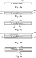
- Figs. 4 represents different steps of the manufacturing of a power module cooled by a liquid cooled busbar.
- the power module is composed of two sub-modules which have a multilayer structure like PCBs, the differents steps of Figs. 4 represent the manufacturing of one of the sub-modules.
- the Fig. 4a represents a base layer 400 that is an electrically non-conductive and thermally conductive material.
- the base layer 400 is made of FR4.
- the base layer 400 is cut, for example by laser cut, in order to form a cavity of the size of a power die 401.
- the power die 401 die is then placed in the cavity.
- the base layer may be divided in two or several layers separated by at least one higher thermally conductive layer 402 such as metals like copper in order to increase heat spreading.
- the Fig. 4b represents the base layer 400 and the power die 401 on which a thin isolation layer 403 is laminated on the top of the base layer 400 and a thin isolation layer 406 is laminated on the bottom of the base layer 400. Furthermore, electrically conducting layers 404 and 405, for example made of copper, are laminated on the thin isolation layers 403 and 406. It has to be noted here that the same operation is performed of the other sub-module.
- the Fig. 4c represents the next step of the power module manufacturing.
- Laser drilling and metallization 407, 409 and 410 are then made in order to connect the power die 401 to the conductor layer.
- the power die contact to the conductor layers can cover completely the power die top and bottom surface or partially by using multiple via connections or other shapes.
- the conductor layers are etched, for example by a chemical or a mechanical process in order to obtain the desired layout on the thin conductor layer.
- the Fig. 4d represents the next step of the power module manufacturing.
- Additional thin isolation layers 411 and 412 and a thick conductor layers 413 and 414 are laminated on both sides of the assembly as obtained in Fig. 4c .
- the Fig. 4e represents the next step of the power module manufacturing.
- laser drilling and metallization (415 and 416) are then made in order to connect the thin conductors layers 404 and 405 and the thick conductor layers 413 and 414.
- the connection can be made through multiple via connections or through other shapes like mettalized copper squares.
- the conductor layers are etched in order to obtain the desired layout on layers 413 and 414. Note that in some particular cases where the conductor layers 413 and 414 are very thick, they can be pre-etched before lamination.
- the Fig. 4f represents the next step of the power module manufacturing.
- Through hole vias 417 are made by drilling then metallizing. Also, board machining or drilling is performed in order to place capacitors 418 and magnetic materials.
- each sub-module is formed by two thin and two thick conductor layers.
- the lamination steps of conductors and insulation layers can be repeated untill the required number of conductor layers is reached.
- the two sub-modules are then assembled with thermally and electrically conductive materials.
- External component soldering, attachment and magnetic material moulding is performed after the assembly of two submodules.
- the capacitor is connected after assembling the two sub-modules between the top layer of the top submodule and the bottom layer of the bottom sub-module.
- the first part of the inductor is made on the first submodule and the second part is made on the second sub-module.
- Fig. 5 represents an example of an electric circuit of a power module that can be cooled by a liquid cooled busbar.
- Each power module comprises a gate driver that provides gate signals to the power dies D1 and D2.
- the drain of the power die D1 is connected to the positive electric potential DC+ provided by the liquid cooled busbar.
- the source of the power die D1 is connected to the drain of the power die D2 and to a first terminal of an inductor L1.
- the source of the power die D2 is connected to the negative electric potential DC- provided by the liquid cooled busbar.
- the second terminal of the inductor L1 is the ouptut of the power module.
Landscapes
- Cooling Or The Like Of Semiconductors Or Solid State Devices (AREA)
- Inverter Devices (AREA)
- Cooling Or The Like Of Electrical Apparatus (AREA)
Abstract
Description
- The present invention relates generally to a system comprising at least one power module comprising at least one power die that is cooled by a liquid cooled system.
- Traditional power converters include power semiconductors which are attached from the bottom side to a substrate, for example, a direct copper bonding (DCB) and are connected by wire bonding on the top side of the dies. This assembly is placed on a metallic base plate in order to spread the heat and then boxed into thermoplastic materials to protect from environmental stress. The obtained power module is attached on a bulky heat sink and the electrical connections are made thanks to a busbar.
- High power density in power electronic applications has always been a priority. With the emergence of wide band gap materials, the power modules have shrunk in size and the power density of power stages has increased. The increase of switching frequency also allows to reduce the size of passive components. However, this trend makes that the power modules have less room for heat sinks.
- To that end, the present invention concerns a system comprising at least one power module comprising at least one power die that is cooled by a liquid cooled system, the liquid cooled system is arranged to provide at least one electric potential to each power dies of the power module, characterized in that the liquid cooled system is composed of a first and a second current-carying bars connected together by an electrically non-conductive pipe, the first bar is placed on the top of the power module and provides a first electric potential to the power die and the second bar is placed on the bottom of the power module and provides a second electric potential to the power dies, the liquid coolant is electrically conductive and the channels surfaces are covered by an electrical insulation layer.
- Thus, the size and cost of a power module can be reduced thanks to the multifunctional busbar.
- Furthermore, the power module is efficiently cooled by a double sided cooling system on the entire heat exchange area with no need to additional room for electrical connection. Any type of liquid coolant can be used with no risk of short circuit between the different bars being at different voltage levels.
- According to a particular feature, the first bar comprises a channel, the second bar comprises a channel, the channels being joint together by the pipe through which a liquid coolant flows.
- Thus, a single coolant circuit is required.
- Thus, any type of liquid coolant can be used with no risk of short circuit between the different bars being at different voltage levels.
- According to a particular feature, fins are introduced in each channel or each channel is split into a plurality of sub-channels.
- Thus, the heat exchange area is increased and the heat convection is increased between liquid coolant and cooler without increasing the pressure drop inside the channels.
- According to a particular feature, the inner surface of the channels have a surface treatment.
- Thus, the heat convection between the cooler and the coolant is increased.
- According to a particular feature, the liquid cooled system is arranged to provide at least one electric power supply to a plurality of dies of power modules.
- According to a particular feature, the power modules are identical and have a rectangular shape and the liquid cooled system is disposed perpendicularly to the larger side of the power modules.
- Thus, a single or multiple power modules are used to build a single or multiple modular power converter composed of a similar power modules and electrically supplied by the same cooling system.
- According to a particular feature, each power module is a multilayer structure formed with isolation and conductor layers and the power dies are embedded in the multilayer structure.
- Thus, the power dies have low inductance connection to the conductor layers of the module.
- According to a particular feature, each power module further comprises capacitors that are embedded in the multilayer structure.
- Thus, the parasitic inductances of the bus capacitors are reduced and therefore the noise generated by the switching transitions of the power module are reduced.
- According to a particular feature, each power module further comprises driving circuits of the power dies that are disposed on a surface of the multilayer structure or integrated completly or partially in the multilayer structure.
- Thus, gate driver circuit is close to the power stage which allows increasing the switching speed and therefore reduce the switching losses of the power dies.
- According to a particular feature, each power module further comprises an inductor that is located within the multilayer structure and a magnetic material that is disposed on a surface of the multilayer structure.
- Thus, the tolerences between power modules are reduced in order to reduce the current disparity between modules in modular power converters.
- According to a particular feature, only the part of the multilayer structure comprising the power die is cooled by the liquid cooled system.
- The characteristics of the invention will emerge more clearly from a reading of the following description of an example of embodiment, the said description being produced with reference to the accompanying drawings, among which:
-
Fig. 1 is a diagram representing a first example of a section of a power module cooled by a liquid cooled busbar according to the present invention; -
Fig. 2 is a diagram representing a power module cooled by a liquid cooled busbar according to the present invention; -
Fig. 3 is a diagram representing an assembly of power modules cooled by a liquid cooled busbar according to the present invention; -
Figs. 4 represents different steps of the manufacturing of a power module cooled by a liquid cooled busbar; -
Fig. 5 represents an electric circuit of a power module cooled by a liquid cooled busbar. -
Fig. 1 is a diagram representing a first example of a section of a power module cooled by a liquid cooled busbar according to the invention. - In the example of
Fig. 1 , the liquid cooled busbar is composed of twobars Fig. 1 that can be mounted on the busbar itself or can be connected to the busbar by pipes or tubes. - The liquid cooled busbar may have any geometrical features, anchors, and/or holes in order to act as mechanical fixture to the power modules PM1 and PM2 to be cooled. According to the invention, the liquid cooled busbar has at least one electrical terminal in order to provide electric potential to the power modules PM1 and PM2. In the example of
Fig. 1 , the liquid cooled busbar has two electric terminals noted DC+ and DC-. The liquid cooled busbar can be made by a multilayer structure attached by any conventional technique like for example sinter, solder or adhesives. The liquid cooled busbar may also be made with other conventional techniques like mechanical machining or other. - The
first bar 10a is linked to the top of power modules PM1 and PM2 through electrically and thermally conductinginterface sheets first bar 10a provides a negative DC voltage to the power modules PM1 and PM2. - The
second bar 10b is linked to the bottom of power modules PM1 and PM2 through electrically and thermally conductinginterface sheets - The
second bar 10b provides a positive DC voltage to the power modules PM1 and PM2. - The first and second bars comprise a channel though which a coolant fluid can flow.
- The first and second bars are mechanically linked using a pipe noted 16. The
pipe 16 has electrical isolation property. - The coolant fluid enters into the channel of the
bar 10b at IN, goes through the channel of the second bar, reaches the channel of the first bar through thepipe 16 and goes out of the liquid cooled busbard through the aperture OUT. - The coolant fluid is electrically conducting, the channel surfaces are covered by an electrical insulation layer noted 11a and 11b.
- The two bars are attached to each other by electricaly insulated or electrically nonconductive screws and bolts not shown in
Fig. 1 in order to make a pressure and an electric contact between thebars - The inner 11a and 11b of the channels are coated with isolation materials that are also good thermal conductors (organic, ceramic, etc.). The coating can be made by any deposition method such as screen printing, sputtering or others. The
bars -
Fig. 2 is a diagram representing a power module cooled by a liquid cooled busbar. - The power module, for example the power module PM1, is an assembly of two sub-modules which have a multilayer structure like PCB. Each of the sub-modules has at least one embedded semiconductor die such as SiC MOSFET, IGBT or other. The power module assembly will be disclosed in more details in reference to
Figs. 4 . - Very close to the power dies which form the power stage of the power module, capacitors are embedded within the multilayer structure, i.e in the substrate of the power module as bus capacitors in order to smooth the bus voltage.
- The part comprising the power dies is cooled by the liquid cooled busbar composed of two
bars - In the example of
Fig. 2 , eachbar - According to a variant, fins are introduced in each channel.The channel noted 23a of the
bar 20a is connected to thechannel 23b of thebar 20b as other channels shown inFig. 2 . - In the same multilayer structure, additional components can also be embedded like control integrated circuits noted 25, inductors, transformers, sensors, additional capacitors or resistors noted 26.
- Also, embedded into the multilayer structure or mounted on the outer surface of the power modules, additional components can be attached by soldering or other to include additional or complementary functionalities to the power modules. The surfaces of the power modules above and under the power dies are made of copper with or without finishing in order to enable the bus connections of the power modules.
-
Fig. 3 is a diagram representing an assembly of power modules cooled by a liquid cooled busbar. - In the example of
Fig. 3 , a liquid cooledbusbar 30 comprising one input and one output cools five power modules PM31 to PM35. - The liquid cooled busbar is not, as already disclosed composed of two bars but is composed in the example of
Fig. 3 of a single bar that cools the power dies by from the bottom and provides at the same a DC electric potential to the power modules PM31 to PM35. - It has to be noted here that the liquid cooled busbar may also be composed of two bars.
-
Figs. 4 represents different steps of the manufacturing of a power module cooled by a liquid cooled busbar. - The power module is composed of two sub-modules which have a multilayer structure like PCBs, the differents steps of
Figs. 4 represent the manufacturing of one of the sub-modules. - The
Fig. 4a represents abase layer 400 that is an electrically non-conductive and thermally conductive material. For example thebase layer 400 is made of FR4. Thebase layer 400 is cut, for example by laser cut, in order to form a cavity of the size of apower die 401. The power die 401 die is then placed in the cavity. The base layer may be divided in two or several layers separated by at least one higher thermallyconductive layer 402 such as metals like copper in order to increase heat spreading. - The
Fig. 4b represents thebase layer 400 and the power die 401 on which athin isolation layer 403 is laminated on the top of thebase layer 400 and athin isolation layer 406 is laminated on the bottom of thebase layer 400. Furthermore, electrically conductinglayers - The
Fig. 4c represents the next step of the power module manufacturing. - Laser drilling and
metallization - The
Fig. 4d represents the next step of the power module manufacturing. - Additional thin isolation layers 411 and 412 and a thick conductor layers 413 and 414 are laminated on both sides of the assembly as obtained in
Fig. 4c . - The
Fig. 4e represents the next step of the power module manufacturing. - Once again, laser drilling and metallization (415 and 416) are then made in order to connect the thin conductors layers 404 and 405 and the thick conductor layers 413 and 414. The connection can be made through multiple via connections or through other shapes like mettalized copper squares. The conductor layers are etched in order to obtain the desired layout on
layers - The
Fig. 4f represents the next step of the power module manufacturing. - Through hole vias 417 are made by drilling then metallizing. Also, board machining or drilling is performed in order to place
capacitors 418 and magnetic materials. - It has to be noted here that in the example of
Fig. 4 , each sub-module is formed by two thin and two thick conductor layers. However, in the general case, the lamination steps of conductors and insulation layers can be repeated untill the required number of conductor layers is reached. - The two sub-modules are then assembled with thermally and electrically conductive materials.
- External component soldering, attachment and magnetic material moulding is performed after the assembly of two submodules.
- The capacitor is connected after assembling the two sub-modules between the top layer of the top submodule and the bottom layer of the bottom sub-module.
- The first part of the inductor is made on the first submodule and the second part is made on the second sub-module.
-
Fig. 5 represents an example of an electric circuit of a power module that can be cooled by a liquid cooled busbar. - Each power module comprises a gate driver that provides gate signals to the power dies D1 and D2.
- The drain of the power die D1 is connected to the positive electric potential DC+ provided by the liquid cooled busbar. The source of the power die D1 is connected to the drain of the power die D2 and to a first terminal of an inductor L1.
- The source of the power die D2 is connected to the negative electric potential DC- provided by the liquid cooled busbar.
- The second terminal of the inductor L1 is the ouptut of the power module.
- Naturally, many modifications can be made to the embodiments of the invention described above without departing from the scope of the present invention.
Claims (11)
- A system comprising at least one power module comprising at least one power die that is cooled by a liquid cooled system, the liquid cooled system is arranged to provide at least one electric potential to each power dies of the power module, characterized in that the liquid cooled system is composed of a first and a second current-carying bars connected together by an electrically non-conductive pipe, the first bar is placed on the top of the power module and provides a first electric potential to the power die and the second bar is placed on the bottom of the power module and provides a second electric potential to the power dies, the liquid coolant is electrically conductive and the channels surfaces are covered by an electrical insulation layer.
- The system according to claim 1, characterized in that the first bar comprises a channel, the second bar comprises a channel, the channels being joint together by the electrically non-conductive pipe through which a liquid coolant flows.
- The system according to any of the claims 1 to 2, characterized in that fins are introduced in each channel or each channel is split into a plurality of sub-channels.
- The system according to any of the claims 2 to 3, characterized in that the inner surface of the channels has a surface treatment.
- The system according to any of the claims 1 to 4, characterized in that the liquid cooled system is arranged to provide at least one electric power supply to a plurality of dies of power modules.
- The system accoding to claim 5, characterized in that the power modules are identical and have a rectangular shape and in that the liquid cooled system is disposed perpendicularly to the larger side of the power modules.
- The system according to claim 5 or 6, characterized in that each power module is a multilayer structure formed with isolation and conductor layers and the power dies are embedded in the multilayer structure.
- The system according to claim 7, characterized in that each power module further comprises capacitors that are embedded in the multilayer structure.
- The system according to claim 8, characterized in that each power module further comprises driving circuits of the power dies that are disposed on a surface of the multilayer structure or integrated completly or partially in the multilayer structure.
- The system according to claim 9, characterized in that each power module further comprises an inductor that is located within the multilayer structure and a magnetic material that is disposed on a surface of the multilayer structure.
- The system according to claim 10, characterized in that only the part of the multilayer structure comprising the power die is cooled by the liquid cooled system.
Priority Applications (6)
| Application Number | Priority Date | Filing Date | Title |
|---|---|---|---|
| ES16171014T ES2773479T3 (en) | 2016-05-24 | 2016-05-24 | System comprising at least one power module comprising at least one power chip that is cooled with a liquid cooled busbar |
| EP16171014.0A EP3249685B1 (en) | 2016-05-24 | 2016-05-24 | System comprising at least one power module comprising at least one power die that is cooled by a liquid cooled busbar |
| PCT/JP2017/017324 WO2017203960A1 (en) | 2016-05-24 | 2017-04-25 | System comprising at least one power module comprising at least one power die that is cooled by liquid cooled system |
| US16/090,859 US10985088B2 (en) | 2016-05-24 | 2017-04-25 | System comprising at least one power module comprising at least one power die that is cooled by liquid cooled system |
| CN201780026696.7A CN109155297A (en) | 2016-05-24 | 2017-04-25 | System including at least one power module containing at least one power die cooled down by liquid cooling system |
| JP2018534893A JP6537739B2 (en) | 2016-05-24 | 2017-04-25 | System comprising at least one power module comprising at least one power die cooled by a liquid cooling system |
Applications Claiming Priority (1)
| Application Number | Priority Date | Filing Date | Title |
|---|---|---|---|
| EP16171014.0A EP3249685B1 (en) | 2016-05-24 | 2016-05-24 | System comprising at least one power module comprising at least one power die that is cooled by a liquid cooled busbar |
Publications (2)
| Publication Number | Publication Date |
|---|---|
| EP3249685A1 true EP3249685A1 (en) | 2017-11-29 |
| EP3249685B1 EP3249685B1 (en) | 2019-11-27 |
Family
ID=56080286
Family Applications (1)
| Application Number | Title | Priority Date | Filing Date |
|---|---|---|---|
| EP16171014.0A Active EP3249685B1 (en) | 2016-05-24 | 2016-05-24 | System comprising at least one power module comprising at least one power die that is cooled by a liquid cooled busbar |
Country Status (6)
| Country | Link |
|---|---|
| US (1) | US10985088B2 (en) |
| EP (1) | EP3249685B1 (en) |
| JP (1) | JP6537739B2 (en) |
| CN (1) | CN109155297A (en) |
| ES (1) | ES2773479T3 (en) |
| WO (1) | WO2017203960A1 (en) |
Cited By (1)
| Publication number | Priority date | Publication date | Assignee | Title |
|---|---|---|---|---|
| US20210092878A1 (en) * | 2019-09-25 | 2021-03-25 | Baidu Usa Llc | Cooling devices for edge computing and heterogeneous computing electronics hardware |
Families Citing this family (6)
| Publication number | Priority date | Publication date | Assignee | Title |
|---|---|---|---|---|
| FR3079664B1 (en) * | 2018-03-30 | 2020-04-24 | Institut Vedecom | MODULAR POWER SWITCHING ELEMENT AND DEMOUNTABLE ASSEMBLY OF SEVERAL MODULAR ELEMENTS |
| US11967899B2 (en) | 2020-05-22 | 2024-04-23 | Marel Power Solutions | Fluid cooled inverter |
| CA3184264A1 (en) * | 2020-05-22 | 2021-11-25 | Marel Power Solutions, Inc. | Compact inverter system |
| EP4135029A1 (en) | 2021-08-11 | 2023-02-15 | Hamilton Sundstrand Corporation | Power semiconductor cooling assembly |
| US12193202B2 (en) | 2021-09-15 | 2025-01-07 | Marel Power Solutions, Inc. | Air cooled compact power systems |
| CN118370008A (en) | 2021-09-15 | 2024-07-19 | 马雷尔动力解决方案股份有限公司 | Air-cooled power converter |
Citations (2)
| Publication number | Priority date | Publication date | Assignee | Title |
|---|---|---|---|---|
| US6501172B1 (en) * | 2000-05-25 | 2002-12-31 | Mitsubishi Denki Kabushiki Kaisha | Power module |
| DE102014223261A1 (en) * | 2014-11-14 | 2016-05-19 | Siemens Aktiengesellschaft | High voltage DC transmission system with a conductivity sensor |
Family Cites Families (18)
| Publication number | Priority date | Publication date | Assignee | Title |
|---|---|---|---|---|
| CH629913A5 (en) * | 1977-07-12 | 1982-05-14 | Asea Ab | LIQUID-COOLED THYRISTOR VALVE. |
| US5111280A (en) * | 1988-11-10 | 1992-05-05 | Iversen Arthur H | Thermal management of power conditioning systems |
| DE19950026B4 (en) * | 1999-10-09 | 2010-11-11 | Robert Bosch Gmbh | The power semiconductor module |
| JP4120876B2 (en) * | 2003-05-26 | 2008-07-16 | 株式会社デンソー | Semiconductor device |
| JP4979909B2 (en) * | 2005-08-19 | 2012-07-18 | 株式会社日立製作所 | Power converter |
| JP4450230B2 (en) * | 2005-12-26 | 2010-04-14 | 株式会社デンソー | Semiconductor device |
| JP2007251076A (en) * | 2006-03-20 | 2007-09-27 | Hitachi Ltd | Power semiconductor module |
| JP4564937B2 (en) * | 2006-04-27 | 2010-10-20 | 日立オートモティブシステムズ株式会社 | Electric circuit device, electric circuit module, and power conversion device |
| JP2008251647A (en) * | 2007-03-29 | 2008-10-16 | Shindengen Electric Mfg Co Ltd | Heat-dissipating structure of electronic component |
| JP5557441B2 (en) * | 2008-10-31 | 2014-07-23 | 日立オートモティブシステムズ株式会社 | Power converter and electric vehicle |
| CN102906497B (en) * | 2010-01-27 | 2016-08-17 | 熔合Uv系统公司 | High thermal load light-emitting devices cooled by microchannels |
| JP2012174856A (en) * | 2011-02-21 | 2012-09-10 | Hitachi Cable Ltd | Heat sink and manufacturing method of the same |
| JP5941787B2 (en) * | 2012-08-09 | 2016-06-29 | 日立オートモティブシステムズ株式会社 | Power module and method for manufacturing power module |
| JP5694278B2 (en) * | 2012-11-21 | 2015-04-01 | 三菱電機株式会社 | Power converter |
| US8988860B2 (en) * | 2012-11-29 | 2015-03-24 | Siemens Aktiengesellschaft | Power supplies having power electronic modules and replacement methods thereof |
| JP5726215B2 (en) * | 2013-01-11 | 2015-05-27 | 株式会社豊田中央研究所 | Cooling type switching element module |
| GB2526172B (en) * | 2014-03-28 | 2018-12-19 | Deere & Co | Electronic assembly for an inverter |
| JP6469720B2 (en) * | 2014-11-13 | 2019-02-13 | 日立オートモティブシステムズ株式会社 | Power converter |
-
2016
- 2016-05-24 EP EP16171014.0A patent/EP3249685B1/en active Active
- 2016-05-24 ES ES16171014T patent/ES2773479T3/en active Active
-
2017
- 2017-04-25 CN CN201780026696.7A patent/CN109155297A/en active Pending
- 2017-04-25 US US16/090,859 patent/US10985088B2/en not_active Expired - Fee Related
- 2017-04-25 JP JP2018534893A patent/JP6537739B2/en not_active Expired - Fee Related
- 2017-04-25 WO PCT/JP2017/017324 patent/WO2017203960A1/en not_active Ceased
Patent Citations (2)
| Publication number | Priority date | Publication date | Assignee | Title |
|---|---|---|---|---|
| US6501172B1 (en) * | 2000-05-25 | 2002-12-31 | Mitsubishi Denki Kabushiki Kaisha | Power module |
| DE102014223261A1 (en) * | 2014-11-14 | 2016-05-19 | Siemens Aktiengesellschaft | High voltage DC transmission system with a conductivity sensor |
Cited By (2)
| Publication number | Priority date | Publication date | Assignee | Title |
|---|---|---|---|---|
| US20210092878A1 (en) * | 2019-09-25 | 2021-03-25 | Baidu Usa Llc | Cooling devices for edge computing and heterogeneous computing electronics hardware |
| US11382241B2 (en) * | 2019-09-25 | 2022-07-05 | Baidu Usa Llc | Cooling devices for edge computing and heterogeneous computing electronics hardware |
Also Published As
| Publication number | Publication date |
|---|---|
| US10985088B2 (en) | 2021-04-20 |
| ES2773479T3 (en) | 2020-07-13 |
| WO2017203960A1 (en) | 2017-11-30 |
| JP2019502267A (en) | 2019-01-24 |
| JP6537739B2 (en) | 2019-07-03 |
| US20200144156A1 (en) | 2020-05-07 |
| CN109155297A (en) | 2019-01-04 |
| EP3249685B1 (en) | 2019-11-27 |
Similar Documents
| Publication | Publication Date | Title |
|---|---|---|
| EP3249685B1 (en) | System comprising at least one power module comprising at least one power die that is cooled by a liquid cooled busbar | |
| EP2988328B1 (en) | Power semiconductor module and method of manufacturing the same | |
| CN109155298B (en) | Power module and method for manufacturing power module | |
| US20160027711A1 (en) | Semiconductor module | |
| CN114008774A (en) | Electronic circuit and method for producing an electronic circuit | |
| US10154593B2 (en) | Electronic assembly group and method for producing the same | |
| KR20090005190A (en) | Electronic component module | |
| CN112713120A (en) | Power electronic component and method for producing the same | |
| CN110268520B (en) | Method for integrating power chips and forming bus bars of heat sink | |
| US20220322582A1 (en) | Systems including an integrated power module with vias and methods of forming the same | |
| EP4016618B1 (en) | Power device packaging | |
| US11515804B2 (en) | Electrical power circuit for an electrical power converter | |
| CN110383473B (en) | Power electronic circuit equipped with bus bars forming heat sink and method of integration | |
| US20240128197A1 (en) | Assemblies with embedded semiconductor device modules and related methods | |
| US20250349640A1 (en) | Semiconductor Package and Array of Semiconductor Packages | |
| US12284792B2 (en) | Power electronics assemblies having power electronics devices embedded within a flip chip | |
| US20260123408A1 (en) | Electronic device cooling with integrated magnetics | |
| CN118588696B (en) | A power module | |
| WO2025256741A1 (en) | Power supply assembly | |
| Boettcher et al. | Embedded die packages and modules for power electronics applications | |
| CN111937146B (en) | Modular power switching element and removable assembly of a plurality of modular elements | |
| WO2023244781A1 (en) | Cooling structure of a power supply module |
Legal Events
| Date | Code | Title | Description |
|---|---|---|---|
| PUAI | Public reference made under article 153(3) epc to a published international application that has entered the european phase |
Free format text: ORIGINAL CODE: 0009012 |
|
| STAA | Information on the status of an ep patent application or granted ep patent |
Free format text: STATUS: THE APPLICATION HAS BEEN PUBLISHED |
|
| AK | Designated contracting states |
Kind code of ref document: A1 Designated state(s): AL AT BE BG CH CY CZ DE DK EE ES FI FR GB GR HR HU IE IS IT LI LT LU LV MC MK MT NL NO PL PT RO RS SE SI SK SM TR |
|
| AX | Request for extension of the european patent |
Extension state: BA ME |
|
| STAA | Information on the status of an ep patent application or granted ep patent |
Free format text: STATUS: REQUEST FOR EXAMINATION WAS MADE |
|
| 17P | Request for examination filed |
Effective date: 20180806 |
|
| RBV | Designated contracting states (corrected) |
Designated state(s): AL AT BE BG CH CY CZ DE DK EE ES FI FR GB GR HR HU IE IS IT LI LT LU LV MC MK MT NL NO PL PT RO RS SE SI SK SM TR |
|
| GRAP | Despatch of communication of intention to grant a patent |
Free format text: ORIGINAL CODE: EPIDOSNIGR1 |
|
| STAA | Information on the status of an ep patent application or granted ep patent |
Free format text: STATUS: GRANT OF PATENT IS INTENDED |
|
| INTG | Intention to grant announced |
Effective date: 20190621 |
|
| GRAS | Grant fee paid |
Free format text: ORIGINAL CODE: EPIDOSNIGR3 |
|
| GRAA | (expected) grant |
Free format text: ORIGINAL CODE: 0009210 |
|
| STAA | Information on the status of an ep patent application or granted ep patent |
Free format text: STATUS: THE PATENT HAS BEEN GRANTED |
|
| AK | Designated contracting states |
Kind code of ref document: B1 Designated state(s): AL AT BE BG CH CY CZ DE DK EE ES FI FR GB GR HR HU IE IS IT LI LT LU LV MC MK MT NL NO PL PT RO RS SE SI SK SM TR |
|
| REG | Reference to a national code |
Ref country code: GB Ref legal event code: FG4D |
|
| REG | Reference to a national code |
Ref country code: CH Ref legal event code: EP |
|
| REG | Reference to a national code |
Ref country code: AT Ref legal event code: REF Ref document number: 1207668 Country of ref document: AT Kind code of ref document: T Effective date: 20191215 |
|
| REG | Reference to a national code |
Ref country code: DE Ref legal event code: R096 Ref document number: 602016024934 Country of ref document: DE |
|
| REG | Reference to a national code |
Ref country code: IE Ref legal event code: FG4D |
|
| REG | Reference to a national code |
Ref country code: NL Ref legal event code: MP Effective date: 20191127 |
|
| REG | Reference to a national code |
Ref country code: LT Ref legal event code: MG4D |
|
| PG25 | Lapsed in a contracting state [announced via postgrant information from national office to epo] |
Ref country code: BG Free format text: LAPSE BECAUSE OF FAILURE TO SUBMIT A TRANSLATION OF THE DESCRIPTION OR TO PAY THE FEE WITHIN THE PRESCRIBED TIME-LIMIT Effective date: 20200227 Ref country code: NO Free format text: LAPSE BECAUSE OF FAILURE TO SUBMIT A TRANSLATION OF THE DESCRIPTION OR TO PAY THE FEE WITHIN THE PRESCRIBED TIME-LIMIT Effective date: 20200227 Ref country code: LT Free format text: LAPSE BECAUSE OF FAILURE TO SUBMIT A TRANSLATION OF THE DESCRIPTION OR TO PAY THE FEE WITHIN THE PRESCRIBED TIME-LIMIT Effective date: 20191127 Ref country code: FI Free format text: LAPSE BECAUSE OF FAILURE TO SUBMIT A TRANSLATION OF THE DESCRIPTION OR TO PAY THE FEE WITHIN THE PRESCRIBED TIME-LIMIT Effective date: 20191127 Ref country code: NL Free format text: LAPSE BECAUSE OF FAILURE TO SUBMIT A TRANSLATION OF THE DESCRIPTION OR TO PAY THE FEE WITHIN THE PRESCRIBED TIME-LIMIT Effective date: 20191127 Ref country code: SE Free format text: LAPSE BECAUSE OF FAILURE TO SUBMIT A TRANSLATION OF THE DESCRIPTION OR TO PAY THE FEE WITHIN THE PRESCRIBED TIME-LIMIT Effective date: 20191127 Ref country code: LV Free format text: LAPSE BECAUSE OF FAILURE TO SUBMIT A TRANSLATION OF THE DESCRIPTION OR TO PAY THE FEE WITHIN THE PRESCRIBED TIME-LIMIT Effective date: 20191127 Ref country code: GR Free format text: LAPSE BECAUSE OF FAILURE TO SUBMIT A TRANSLATION OF THE DESCRIPTION OR TO PAY THE FEE WITHIN THE PRESCRIBED TIME-LIMIT Effective date: 20200228 |
|
| PG25 | Lapsed in a contracting state [announced via postgrant information from national office to epo] |
Ref country code: RS Free format text: LAPSE BECAUSE OF FAILURE TO SUBMIT A TRANSLATION OF THE DESCRIPTION OR TO PAY THE FEE WITHIN THE PRESCRIBED TIME-LIMIT Effective date: 20191127 Ref country code: HR Free format text: LAPSE BECAUSE OF FAILURE TO SUBMIT A TRANSLATION OF THE DESCRIPTION OR TO PAY THE FEE WITHIN THE PRESCRIBED TIME-LIMIT Effective date: 20191127 Ref country code: IS Free format text: LAPSE BECAUSE OF FAILURE TO SUBMIT A TRANSLATION OF THE DESCRIPTION OR TO PAY THE FEE WITHIN THE PRESCRIBED TIME-LIMIT Effective date: 20200327 |
|
| PG25 | Lapsed in a contracting state [announced via postgrant information from national office to epo] |
Ref country code: AL Free format text: LAPSE BECAUSE OF FAILURE TO SUBMIT A TRANSLATION OF THE DESCRIPTION OR TO PAY THE FEE WITHIN THE PRESCRIBED TIME-LIMIT Effective date: 20191127 |
|
| REG | Reference to a national code |
Ref country code: ES Ref legal event code: FG2A Ref document number: 2773479 Country of ref document: ES Kind code of ref document: T3 Effective date: 20200713 |
|
| PG25 | Lapsed in a contracting state [announced via postgrant information from national office to epo] |
Ref country code: PT Free format text: LAPSE BECAUSE OF FAILURE TO SUBMIT A TRANSLATION OF THE DESCRIPTION OR TO PAY THE FEE WITHIN THE PRESCRIBED TIME-LIMIT Effective date: 20200419 Ref country code: RO Free format text: LAPSE BECAUSE OF FAILURE TO SUBMIT A TRANSLATION OF THE DESCRIPTION OR TO PAY THE FEE WITHIN THE PRESCRIBED TIME-LIMIT Effective date: 20191127 Ref country code: EE Free format text: LAPSE BECAUSE OF FAILURE TO SUBMIT A TRANSLATION OF THE DESCRIPTION OR TO PAY THE FEE WITHIN THE PRESCRIBED TIME-LIMIT Effective date: 20191127 Ref country code: CZ Free format text: LAPSE BECAUSE OF FAILURE TO SUBMIT A TRANSLATION OF THE DESCRIPTION OR TO PAY THE FEE WITHIN THE PRESCRIBED TIME-LIMIT Effective date: 20191127 Ref country code: DK Free format text: LAPSE BECAUSE OF FAILURE TO SUBMIT A TRANSLATION OF THE DESCRIPTION OR TO PAY THE FEE WITHIN THE PRESCRIBED TIME-LIMIT Effective date: 20191127 |
|
| REG | Reference to a national code |
Ref country code: DE Ref legal event code: R097 Ref document number: 602016024934 Country of ref document: DE |
|
| PG25 | Lapsed in a contracting state [announced via postgrant information from national office to epo] |
Ref country code: SM Free format text: LAPSE BECAUSE OF FAILURE TO SUBMIT A TRANSLATION OF THE DESCRIPTION OR TO PAY THE FEE WITHIN THE PRESCRIBED TIME-LIMIT Effective date: 20191127 Ref country code: SK Free format text: LAPSE BECAUSE OF FAILURE TO SUBMIT A TRANSLATION OF THE DESCRIPTION OR TO PAY THE FEE WITHIN THE PRESCRIBED TIME-LIMIT Effective date: 20191127 |
|
| REG | Reference to a national code |
Ref country code: AT Ref legal event code: MK05 Ref document number: 1207668 Country of ref document: AT Kind code of ref document: T Effective date: 20191127 |
|
| PLBE | No opposition filed within time limit |
Free format text: ORIGINAL CODE: 0009261 |
|
| STAA | Information on the status of an ep patent application or granted ep patent |
Free format text: STATUS: NO OPPOSITION FILED WITHIN TIME LIMIT |
|
| 26N | No opposition filed |
Effective date: 20200828 |
|
| PG25 | Lapsed in a contracting state [announced via postgrant information from national office to epo] |
Ref country code: SI Free format text: LAPSE BECAUSE OF FAILURE TO SUBMIT A TRANSLATION OF THE DESCRIPTION OR TO PAY THE FEE WITHIN THE PRESCRIBED TIME-LIMIT Effective date: 20191127 Ref country code: AT Free format text: LAPSE BECAUSE OF FAILURE TO SUBMIT A TRANSLATION OF THE DESCRIPTION OR TO PAY THE FEE WITHIN THE PRESCRIBED TIME-LIMIT Effective date: 20191127 Ref country code: PL Free format text: LAPSE BECAUSE OF FAILURE TO SUBMIT A TRANSLATION OF THE DESCRIPTION OR TO PAY THE FEE WITHIN THE PRESCRIBED TIME-LIMIT Effective date: 20191127 |
|
| PG25 | Lapsed in a contracting state [announced via postgrant information from national office to epo] |
Ref country code: CH Free format text: LAPSE BECAUSE OF NON-PAYMENT OF DUE FEES Effective date: 20200531 Ref country code: LI Free format text: LAPSE BECAUSE OF NON-PAYMENT OF DUE FEES Effective date: 20200531 Ref country code: MC Free format text: LAPSE BECAUSE OF FAILURE TO SUBMIT A TRANSLATION OF THE DESCRIPTION OR TO PAY THE FEE WITHIN THE PRESCRIBED TIME-LIMIT Effective date: 20191127 |
|
| REG | Reference to a national code |
Ref country code: BE Ref legal event code: MM Effective date: 20200531 |
|
| PG25 | Lapsed in a contracting state [announced via postgrant information from national office to epo] |
Ref country code: LU Free format text: LAPSE BECAUSE OF NON-PAYMENT OF DUE FEES Effective date: 20200524 |
|
| PG25 | Lapsed in a contracting state [announced via postgrant information from national office to epo] |
Ref country code: IE Free format text: LAPSE BECAUSE OF NON-PAYMENT OF DUE FEES Effective date: 20200524 |
|
| PG25 | Lapsed in a contracting state [announced via postgrant information from national office to epo] |
Ref country code: BE Free format text: LAPSE BECAUSE OF NON-PAYMENT OF DUE FEES Effective date: 20200531 |
|
| PGFP | Annual fee paid to national office [announced via postgrant information from national office to epo] |
Ref country code: DE Payment date: 20210527 Year of fee payment: 6 Ref country code: FR Payment date: 20210526 Year of fee payment: 6 Ref country code: IT Payment date: 20210527 Year of fee payment: 6 |
|
| PGFP | Annual fee paid to national office [announced via postgrant information from national office to epo] |
Ref country code: GB Payment date: 20210527 Year of fee payment: 6 |
|
| PGFP | Annual fee paid to national office [announced via postgrant information from national office to epo] |
Ref country code: ES Payment date: 20210721 Year of fee payment: 6 |
|
| PG25 | Lapsed in a contracting state [announced via postgrant information from national office to epo] |
Ref country code: TR Free format text: LAPSE BECAUSE OF FAILURE TO SUBMIT A TRANSLATION OF THE DESCRIPTION OR TO PAY THE FEE WITHIN THE PRESCRIBED TIME-LIMIT Effective date: 20191127 Ref country code: MT Free format text: LAPSE BECAUSE OF FAILURE TO SUBMIT A TRANSLATION OF THE DESCRIPTION OR TO PAY THE FEE WITHIN THE PRESCRIBED TIME-LIMIT Effective date: 20191127 Ref country code: CY Free format text: LAPSE BECAUSE OF FAILURE TO SUBMIT A TRANSLATION OF THE DESCRIPTION OR TO PAY THE FEE WITHIN THE PRESCRIBED TIME-LIMIT Effective date: 20191127 |
|
| PG25 | Lapsed in a contracting state [announced via postgrant information from national office to epo] |
Ref country code: MK Free format text: LAPSE BECAUSE OF FAILURE TO SUBMIT A TRANSLATION OF THE DESCRIPTION OR TO PAY THE FEE WITHIN THE PRESCRIBED TIME-LIMIT Effective date: 20191127 |
|
| REG | Reference to a national code |
Ref country code: DE Ref legal event code: R119 Ref document number: 602016024934 Country of ref document: DE |
|
| GBPC | Gb: european patent ceased through non-payment of renewal fee |
Effective date: 20220524 |
|
| PG25 | Lapsed in a contracting state [announced via postgrant information from national office to epo] |
Ref country code: FR Free format text: LAPSE BECAUSE OF NON-PAYMENT OF DUE FEES Effective date: 20220531 |
|
| PG25 | Lapsed in a contracting state [announced via postgrant information from national office to epo] |
Ref country code: GB Free format text: LAPSE BECAUSE OF NON-PAYMENT OF DUE FEES Effective date: 20220524 Ref country code: DE Free format text: LAPSE BECAUSE OF NON-PAYMENT OF DUE FEES Effective date: 20221201 |
|
| REG | Reference to a national code |
Ref country code: ES Ref legal event code: FD2A Effective date: 20230630 |
|
| PG25 | Lapsed in a contracting state [announced via postgrant information from national office to epo] |
Ref country code: IT Free format text: LAPSE BECAUSE OF NON-PAYMENT OF DUE FEES Effective date: 20220524 Ref country code: ES Free format text: LAPSE BECAUSE OF NON-PAYMENT OF DUE FEES Effective date: 20220525 |