EP3249683A1 - Process for the manufacture of a high resistivity semiconductor substrate - Google Patents
Process for the manufacture of a high resistivity semiconductor substrate Download PDFInfo
- Publication number
- EP3249683A1 EP3249683A1 EP17171861.2A EP17171861A EP3249683A1 EP 3249683 A1 EP3249683 A1 EP 3249683A1 EP 17171861 A EP17171861 A EP 17171861A EP 3249683 A1 EP3249683 A1 EP 3249683A1
- Authority
- EP
- European Patent Office
- Prior art keywords
- substrate
- approximately
- stage
- process according
- layer
- Prior art date
- Legal status (The legal status is an assumption and is not a legal conclusion. Google has not performed a legal analysis and makes no representation as to the accuracy of the status listed.)
- Granted
Links
Images
Classifications
-
- H—ELECTRICITY
- H10—SEMICONDUCTOR DEVICES; ELECTRIC SOLID-STATE DEVICES NOT OTHERWISE PROVIDED FOR
- H10P—GENERIC PROCESSES OR APPARATUS FOR THE MANUFACTURE OR TREATMENT OF DEVICES COVERED BY CLASS H10
- H10P90/00—Preparation of wafers not covered by a single main group of this subclass, e.g. wafer reinforcement
- H10P90/19—Preparing inhomogeneous wafers
- H10P90/1904—Preparing vertically inhomogeneous wafers
- H10P90/1906—Preparing SOI wafers
-
- H—ELECTRICITY
- H10—SEMICONDUCTOR DEVICES; ELECTRIC SOLID-STATE DEVICES NOT OTHERWISE PROVIDED FOR
- H10P—GENERIC PROCESSES OR APPARATUS FOR THE MANUFACTURE OR TREATMENT OF DEVICES COVERED BY CLASS H10
- H10P90/00—Preparation of wafers not covered by a single main group of this subclass, e.g. wafer reinforcement
- H10P90/19—Preparing inhomogeneous wafers
- H10P90/1904—Preparing vertically inhomogeneous wafers
- H10P90/1906—Preparing SOI wafers
- H10P90/1914—Preparing SOI wafers using bonding
- H10P90/1916—Preparing SOI wafers using bonding with separation or delamination along an ion implanted layer, e.g. Smart-cut
-
- H—ELECTRICITY
- H10—SEMICONDUCTOR DEVICES; ELECTRIC SOLID-STATE DEVICES NOT OTHERWISE PROVIDED FOR
- H10P—GENERIC PROCESSES OR APPARATUS FOR THE MANUFACTURE OR TREATMENT OF DEVICES COVERED BY CLASS H10
- H10P32/00—Diffusion of dopants within, into or out of wafers, substrates or parts of devices
- H10P32/10—Diffusion of dopants within, into or out of semiconductor bodies or layers
- H10P32/14—Diffusion of dopants within, into or out of semiconductor bodies or layers within a single semiconductor body or layer in a solid phase; between different semiconductor bodies or layers, both in a solid phase
- H10P32/1404—Diffusion of dopants within, into or out of semiconductor bodies or layers within a single semiconductor body or layer in a solid phase; between different semiconductor bodies or layers, both in a solid phase using predeposition followed by drive-in of impurities into the semiconductor surface, e.g. predeposition from a gaseous phase
- H10P32/1406—Diffusion of dopants within, into or out of semiconductor bodies or layers within a single semiconductor body or layer in a solid phase; between different semiconductor bodies or layers, both in a solid phase using predeposition followed by drive-in of impurities into the semiconductor surface, e.g. predeposition from a gaseous phase by ion implantation
-
- H—ELECTRICITY
- H10—SEMICONDUCTOR DEVICES; ELECTRIC SOLID-STATE DEVICES NOT OTHERWISE PROVIDED FOR
- H10P—GENERIC PROCESSES OR APPARATUS FOR THE MANUFACTURE OR TREATMENT OF DEVICES COVERED BY CLASS H10
- H10P72/00—Handling or holding of wafers, substrates or devices during manufacture or treatment thereof
- H10P72/06—Apparatus for monitoring, sorting, marking, testing or measuring
- H10P72/0602—Temperature monitoring
-
- H—ELECTRICITY
- H10—SEMICONDUCTOR DEVICES; ELECTRIC SOLID-STATE DEVICES NOT OTHERWISE PROVIDED FOR
- H10P—GENERIC PROCESSES OR APPARATUS FOR THE MANUFACTURE OR TREATMENT OF DEVICES COVERED BY CLASS H10
- H10P95/00—Generic processes or apparatus for manufacture or treatments not covered by the other groups of this subclass
- H10P95/90—Thermal treatments, e.g. annealing or sintering
-
- H—ELECTRICITY
- H10—SEMICONDUCTOR DEVICES; ELECTRIC SOLID-STATE DEVICES NOT OTHERWISE PROVIDED FOR
- H10W—GENERIC PACKAGES, INTERCONNECTIONS, CONNECTORS OR OTHER CONSTRUCTIONAL DETAILS OF DEVICES COVERED BY CLASS H10
- H10W10/00—Isolation regions in semiconductor bodies between components of integrated devices
- H10W10/10—Isolation regions comprising dielectric materials
- H10W10/181—Semiconductor-on-insulator [SOI] isolation regions, e.g. buried oxide regions of SOI wafers
-
- H—ELECTRICITY
- H10—SEMICONDUCTOR DEVICES; ELECTRIC SOLID-STATE DEVICES NOT OTHERWISE PROVIDED FOR
- H10P—GENERIC PROCESSES OR APPARATUS FOR THE MANUFACTURE OR TREATMENT OF DEVICES COVERED BY CLASS H10
- H10P10/00—Bonding of wafers, substrates or parts of devices
- H10P10/12—Bonding of semiconductor wafers or semiconductor substrates to semiconductor wafers or semiconductor substrates
- H10P10/128—Bonding of semiconductor wafers or semiconductor substrates to semiconductor wafers or semiconductor substrates by direct semiconductor to semiconductor bonding
-
- H—ELECTRICITY
- H10—SEMICONDUCTOR DEVICES; ELECTRIC SOLID-STATE DEVICES NOT OTHERWISE PROVIDED FOR
- H10P—GENERIC PROCESSES OR APPARATUS FOR THE MANUFACTURE OR TREATMENT OF DEVICES COVERED BY CLASS H10
- H10P30/00—Ion implantation into wafers, substrates or parts of devices
- H10P30/20—Ion implantation into wafers, substrates or parts of devices into semiconductor materials, e.g. for doping
- H10P30/202—Ion implantation into wafers, substrates or parts of devices into semiconductor materials, e.g. for doping characterised by the semiconductor materials
- H10P30/204—Ion implantation into wafers, substrates or parts of devices into semiconductor materials, e.g. for doping characterised by the semiconductor materials into Group IV semiconductors
-
- H—ELECTRICITY
- H10—SEMICONDUCTOR DEVICES; ELECTRIC SOLID-STATE DEVICES NOT OTHERWISE PROVIDED FOR
- H10P—GENERIC PROCESSES OR APPARATUS FOR THE MANUFACTURE OR TREATMENT OF DEVICES COVERED BY CLASS H10
- H10P30/00—Ion implantation into wafers, substrates or parts of devices
- H10P30/20—Ion implantation into wafers, substrates or parts of devices into semiconductor materials, e.g. for doping
- H10P30/208—Ion implantation into wafers, substrates or parts of devices into semiconductor materials, e.g. for doping of electrically inactive species
-
- H—ELECTRICITY
- H10—SEMICONDUCTOR DEVICES; ELECTRIC SOLID-STATE DEVICES NOT OTHERWISE PROVIDED FOR
- H10P—GENERIC PROCESSES OR APPARATUS FOR THE MANUFACTURE OR TREATMENT OF DEVICES COVERED BY CLASS H10
- H10P36/00—Gettering within semiconductor bodies
- H10P36/03—Gettering within semiconductor bodies within silicon bodies
- H10P36/07—Gettering within semiconductor bodies within silicon bodies of silicon-on-insulator structures
-
- H—ELECTRICITY
- H10—SEMICONDUCTOR DEVICES; ELECTRIC SOLID-STATE DEVICES NOT OTHERWISE PROVIDED FOR
- H10P—GENERIC PROCESSES OR APPARATUS FOR THE MANUFACTURE OR TREATMENT OF DEVICES COVERED BY CLASS H10
- H10P90/00—Preparation of wafers not covered by a single main group of this subclass, e.g. wafer reinforcement
- H10P90/19—Preparing inhomogeneous wafers
- H10P90/1904—Preparing vertically inhomogeneous wafers
- H10P90/1906—Preparing SOI wafers
- H10P90/1914—Preparing SOI wafers using bonding
Definitions
- the present invention relates to a process for the manufacture of a high resistivity semiconductor substrate by layer transfer and relates in particular to the improvement in the substrates of the silicon-on-insulator type having a high resistivity and having a high concentration of interstitial oxygen.
- high resistivity is understood to mean approximately 750 ⁇ m or more and “high concentration of interstitial oxygen” is understood to mean approximately 25 ppma or more, i.e. approximately 12.5 ⁇ 10 17 atoms ⁇ cm -3 or more.
- the abovementioned stabilization stage is conventionally carried out during the stage of sacrificial oxidation of the SOI following a layer transfer carried out, for example, by the known SmartCut® technique.
- the stabilization stage is more particularly carried out after a smoothing annealing subsequent to the layer transfer, which is generally a rapid annealing, i.e. RTA ("Rapid Thermal Anneal").
- RTA Rapid Thermal Anneal
- RTA type smoothing annealing
- a process for the manufacture of a high resistivity semiconductor substrate comprising the following stages: providing a first substrate with an in-depth weakened layer; providing a second substrate with a layer of an oxide at the surface; attaching the first substrate to the second substrate so as to form a compound substrate comprising a buried oxide layer; and cleaving the compound substrate at the level of the weakened layer.
- the process comprises at least one stage of stabilization, in particular a stabilization heat treatment, of the second substrate with the oxide layer before the stage of cleaving at the level of the weakened layer.
- the prior art teaches the carrying out of a stabilization stage subsequent to a smoothing annealing stage, which is a stage occurring after the cleaving of the compound substrate at the level of the weakened layer.
- a smoothing annealing stage which is a stage occurring after the cleaving of the compound substrate at the level of the weakened layer.
- the prior art does not teach the carrying out of at least one stabilization stage before the smoothing annealing and in particular before the separation of the weakened layer.
- the said at least one stabilization stage can thus be a stage of nucleation, precipitation and growth of the precipitates, in particular a heat treatment comprising several stationary temperature phases.
- the present invention proposes to carry out the treatments targeted at rendering a substrate having a high concentration of interstitial oxygen highly resistive (nucleation, precipitation), before any smoothing treatment of RTA type, in particular before the cleaving stage, during the preparation of a substrate of SOI type.
- the present invention thus makes it possible to obtain electrical characteristics compatible with the preparation of transistors of CMOS type on such substrates.
- the solution provided by the present invention advantageously makes it possible to use substrates having a high concentration of interstitial oxygen in the preparation of an SOI substrate for applications of RF, photonic, imaging, digital, and the like, type, without having recourse to substrates having a very low concentration of interstitial oxygen which are very sensitive to heat treatments in terms of deformations and defects induced.
- the said at least one stage of stabilization of the second substrate with the oxide layer can be carried out preferably before the stage of attachment of the two substrates.
- the said at least one stabilization stage can, in all cases, be carried out before the cleaving and thus before any smoothing annealing subsequent to the cleaving.
- the first substrate in other words the donor substrate in a layer transfer, can comprise a semiconductor material, in particular silicon, germanium or a compound of silicon and of germanium. More generally, the donor substrate can comprise one or more alloys of semiconductors III-V and/or one or more alloys of semiconductors of Group IV.
- the second substrate can comprise silicon, in particular having a high concentration of interstitial oxygen.
- the second substrate can comprise silicon with a concentration of interstitial oxygen of at least approximately 12 ⁇ 10 17 atoms ⁇ cm -3 .
- the said at least one stabilization stage is a heat treatment comprising several stationary phases at temperatures within the range from approximately 650°C to approximately 1200°C.
- the duration of a stationary temperature phase is within the range extending from approximately 30 min to approximately 10 h, preferably within the range extending from approximately 1 h to approximately 8 h.
- the atmosphere of a stationary temperature phase can be of oxidizing type, in particular based on water and on oxygen, or of nonoxidizing type, in particular neutral type, with a gas based on argon.
- the process can additionally comprise at least one stage of smoothing annealing, in particular a rapid thermal annealing, after the stage of cleaving the compound substrate at the level of the weakened layer. It is thus possible to improve the surface roughness of the substrate after the layer transfer.
- the said at least one stage of smoothing annealing can be carried out at a temperature within the range from approximately 1075°C to approximately 1250°C, preferably from approximately 1175°C to approximately 1230°C, in particular a temperature of approximately 1200°C.
- the said at least one stage of smoothing annealing can be carried out for a period of time within the range of approximately 15 s to approximately 120 s, preferably from approximately 20 s to approximately 90 s, in particular a period of time of approximately 30 s.
- the said at least one stage of smoothing annealing can be carried out under an atmosphere of the nonoxidizing type, in particular comprising argon and/or hydrogen in a composition which can range from 0% to approximately 50% of hydrogen.
- the process can additionally comprise a stage of recycling a residue of the first substrate after the stage of cleaving the compound substrate at the level of the weakened layer. It is thus possible to reuse the residue again as donor substrate for other layer transfer processes.
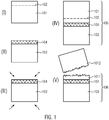
- FIG. 1 A first exemplary embodiment of a process for the manufacture of a high resistivity semiconductor substrate will now be described with reference to Fig. 1 .
- the transfer of a layer of a semiconductor material will be carried out from a donor substrate towards a receiver substrate.
- a donor substrate 101 comprising an in-depth weakened layer 102 is provided for the purpose of carrying out a layer transfer towards a receiver substrate.
- the substrate 101 can be a semiconductor material, for example silicon, germanium or a compound of silicon and of germanium. More generally, the donor substrate can comprise one or more alloys of semiconductors III-V and/or one or more alloys of semiconductors of Group IV.
- a substrate 103 comprising an oxide layer 104 at the surface is also provided for the purpose of receiving a transferred semiconductor layer.
- the substrate 103 can comprise silicon and in particular interstitial oxygen with a concentration of at least approximately 12 ⁇ 10 17 atoms ⁇ cm -3 .
- the oxide layer 104 can be a layer of a natural oxide or a layer of SiO 2 obtained by growth or else deposited.
- the layer 104 can also be, for example, an insulator used in a semiconductor of alumina (Al 2 O 3 ) type or also of nitride type, such as Si 3 N 4 .
- the substrate 103 comprising the oxide layer 104 at the surface is subjected to at least one stage of stabilization treatment of the interstitial oxygen.
- This stage can thus be a stage of nucleation, precipitation and growth of the precipitates.
- It can thus be a heat treatment comprising several stationary temperature phases.
- This treatment, in particular a stationary temperature phase can be carried out under an atmosphere of oxidizing type, in particular based on water and on oxygen, or else under an atmosphere of nonoxidizing type, in particular of neutral type, with a gas based on argon.
- the substrate 103 comprising the oxide layer 104 can thus be subjected to a temperature, in particular to stationary temperature phases, within the range from approximately 650°C to approximately 1200°C. Furthermore, this treatment, in particular each stationary temperature phase, can last for approximately 30 min to approximately 10 h, preferably from approximately 1 h to approximately 8 h.
- the donor substrate 101 is attached, in particular adhesively bonded, for example by molecular adhesion or any other method of adhesively bonding semiconductors, to the receiver substrate 103 via the oxide layer 104, so as to form a compound substrate 105 of the SOI type with a buried oxide layer 104.
- a portion 1012 of the donor substrate 101 is detached from the compound substrate 105 by cleaving at the level of the in-depth weakened layer 102 so as to leave a transferred layer 1011 of the donor substrate 101 attached to the receiver substrate 103 via the oxide layer 104, thus forming a new compound substrate 106 comprising the transferred layer 1011. It is then possible to improve the surface roughness of the transferred layer 1011 by subjecting the compound substrate 106 to one or more smoothing heat treatments, in particular of the rapid annealing, i.e. RTA, type. Furthermore, the residue 1012 of the donor substrate 101 can be recycled to form a new donor substrate in another layer transfer process.
- the compound substrates 105 and 106 are both substrates of HiOi HR SOI type, namely of the type of high resistivity silicon-on-insulator having a high concentration of interstitial oxygen.
- the said at least one stage of stabilization of the interstitial oxygen has been carried out before the layer transfer, in other words before the cleaving stage, and thus before any smoothing annealing, it is possible to obtain HiOi HR SOI substrates with interface state densities of less than 5 ⁇ 10 11 cm -2 ⁇ eV -1 and mobilities of the carriers in the SOI of greater than 700 cm 2 ⁇ V -1 ⁇ s -1 for the electrons.
- the fixed charge values in the buried oxide can then be less than 3 ⁇ 10 10 cm -2 and the crest interface state densities can be less than 5 ⁇ 10 10 cm -2 ⁇ eV -1 .
- the electrical (in particular interfacial) properties of the compound substrates 105 and 106 are very markedly improved in comparison with HiOi HR SOI substrates obtained by conventional methods, that is to say for which the stabilization stage would have been carried out after the smoothing annealing(s).
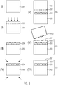
- FIG. 2 A second exemplary embodiment of a process for the manufacture of a high resistivity semiconductor substrate will now be described with reference to Fig. 2 .
- the second embodiment repeats all the characteristics of the first embodiment and in addition gives details of optional process stages.
- a donor substrate 201 which can be the same as the donor substrate 101 of the first embodiment, is first of all provided.
- the substrate 201 can thus also be a semiconductor material, such as silicon, germanium or a compound of silicon and of germanium. More generally, the donor substrate can comprise one or more alloys of semiconductors III-V and/or one or more alloys of semiconductors of Group IV.
- Stage (II) of Fig. 2 illustrates that the donor substrate 201 can subsequently be subjected to a stage of in-depth weakening in order to provide an in-depth weakened layer 202 for the purpose of carrying out a layer transfer towards a receiver substrate, as in the first embodiment.
- This stage can be carried out in particular by ion implantation, especially by implantation of ionic entities, such as H + and/or He + .
- a substrate 203 comprising a layer of oxide 204 at the surface is also provided for the purpose of receiving a transferred semiconductor layer.
- the substrate 203 of the second embodiment can thus comprise silicon and in particular interstitial oxygen with a concentration of at least approximately 12 ⁇ 10 17 atoms ⁇ cm -3 .
- the layer of oxide 204 can once more be a layer of a natural oxide, a layer of SiO 2 , obtained by growth or else deposited, or also an insulator used in semiconductors of alumina (Al 2 O 3 ) type or of nitride type, such as Si 3 N 4 .
- the substrate 203 comprising the layer of oxide 204 at the surface is subjected to at least one stage of stabilization treatment of the interstitial oxygen.
- the stabilization treatment can be a stage of nucleation, precipitation and growth of the precipitates. It can thus be a heat treatment comprising several stationary temperature phases. This treatment, in particular a stationary temperature phase, can be carried out under an atmosphere of oxidizing type, in particular based on water and on oxygen, or else under an atmosphere of nonoxidizing type, in particular of neutral type, with a gas based on argon.
- the substrate 203 comprising the layer of oxide 204 can thus also be subjected to a temperature, in particular to stationary temperature phases, within the range from approximately 650°C to approximately 1200°C. Furthermore, this treatment, in particular each stationary temperature phase, can last from approximately 30 min to approximately 10 h, preferably from approximately 1 h to approximately 8 h.
- the donor substrate 201 and the receiver substrate 203 are adhesively bonded at the level of the layer of oxide 204, so as to form a compound substrate 205 of the SOI type with the layer of buried oxide 204.
- the adhesive bonding can be carried out by molecular adhesion or any other method for the adhesive bonding of semiconductor layers.
- Stage (VI) of Fig. 2 the stage of adhesive bonding is also followed by a stage of cleaving in which a portion 2012 of the donor substrate 201 is detached from the compound substrate 205 by cleaving at the level of the in-depth weakened layer 202, so as to leave a transferred layer 2011 of the donor substrate 201 attached to the receiver substrate 203 by the oxide layer 204, thus forming a new compound substrate 206 comprising the transferred layer 2011.
- a cleaving stage can be carried out by subjecting the compound substrate 205 to a temperature in a range from approximately 300°C to approximately 600°C for a period of time of approximately 30 min to approximately 5 h, under a neutral atmosphere of N 2 or of Ar.
- Stage (VII) of Fig. 2 illustrates an optional subsequent smoothing stage which makes it possible to improve the roughness of the exposed surface 207 of the transferred layer 2011.
- This stage can be carried out by carrying out a heat treatment comprising one or more annealings, preferably one or more rapid annealings, i.e. RTAs.
- the compound substrate 206 can then be exposed to a temperature within a range from approximately 1075°C to approximately 1250°C, preferably from approximately 1175°C to approximately 1230°C, in particular a temperature of approximately 1200°C, this being done for a period of time within the range from approximately 15 s to approximately 120 s, preferably from approximately 20 s to approximately 90 s, in particular a period of time of approximately 30 s, under an atmosphere of the nonoxidizing type, in particular comprising argon and/or hydrogen in a composition which can range from 0% to approximately 50% of hydrogen.
- the residue 2012 of the donor substrate 201 can also be recycled in order to form a new donor substrate in another layer transfer process.
- the second embodiment it is possible in the second embodiment to obtain compound substrates 205 and 206 of HiOi HR SOI type, namely of the type of high resistivity silicon-on-insulator having a high concentration of interstitial oxygen.
- the said at least one stage of stabilization of the interstitial oxygen was carried out before the layer transfer, in other words before the cleaving stage, and thus before any smoothing annealing, just as in the first embodiment, it is possible in the second embodiment to obtain HiOi HR SOI substrates with interface state densities of less than 5 ⁇ 10 11 cm -2 ⁇ eV -1 and mobilities of the carriers in the SOI of greater than 700 cm 2 ⁇ V -1 ⁇ s -1 for the electrons.
- the fixed charge values in the buried oxide can then be less than 3 ⁇ 10 10 cm -2 and the crest interface state densities can be less than 5 ⁇ 10 10 cm -2 ⁇ eV -1 .
- the electrical properties (in particular interfacial properties) of the compound substrates 205 and 206 are also very markedly improved in comparison with HiOi HR SOI substrates obtained by conventional methods, that is to say for which the stabilization stage would have been carried out after the smoothing annealing(s).
Landscapes
- Recrystallisation Techniques (AREA)
- Element Separation (AREA)
Abstract
Description
- The present invention relates to a process for the manufacture of a high resistivity semiconductor substrate by layer transfer and relates in particular to the improvement in the substrates of the silicon-on-insulator type having a high resistivity and having a high concentration of interstitial oxygen.
- It is generally accepted that the use of high resistivity (or "HR") semiconductor substrates of the silicon-on-insulator (or "SOI") type having a high concentration of interstitial oxygen (or "High [Oi]" or else "HiOi") requires the use of heat treatments targeted at stabilizing the oxygen present in the silicon (nucleation, precipitation) in order to render the substrate highly resistive.
- In this context, "high resistivity" is understood to mean approximately 750 Ω·m or more and "high concentration of interstitial oxygen" is understood to mean approximately 25 ppma or more, i.e. approximately 12.5 × 10¹⁷ atoms·cm-3 or more.
- The abovementioned stabilization stage is conventionally carried out during the stage of sacrificial oxidation of the SOI following a layer transfer carried out, for example, by the known SmartCut® technique. Conventionally, the stabilization stage is more particularly carried out after a smoothing annealing subsequent to the layer transfer, which is generally a rapid annealing, i.e. RTA ("Rapid Thermal Anneal"). The published patent application
FR 2 858 462 A1 - On carrying out the electrical characterization of these materials (pseudo-MOS material), abnormally high interface state densities, typically reaching values of at least 20 × 1011 cm-2·eV-1, resulting in a poor mobility of the carriers in the SOI, typically of approximately 400 cm2·V-1·s-1 or less for the electrons, were demonstrated. Additional analyses (C(V) characterization of an MOS capacitor) after removal of the SOI film and aluminium on buried oxide contact have revealed fixed charge values in the buried oxide of at least 5 × 1010 cm-2 and crest interface state densities of at least 2 × 1011 cm-2·eV-1, thus showing that the source of this poor interface quality originated from the interface under the buried oxide.
- One hypothesis put forward is that the smoothing annealing (RTA type) results in the modification of the distribution of the unstabilized oxygen in the substrate, thus bringing about an increase in the amount of traps under the buried oxide.
- One solution for overcoming this problem lies in the use of HR substrates having a very low concentration of interstitial oxygen (i.e., "Low [Oi]"), namely below approximately 12 ppma, i.e. below approximately 6 × 10¹⁷ atoms·cm-3, which do not require stabilization annealing of the oxygen in the silicon (nucleation, precipitation). This is because this type of substrate is naturally highly resistive without having to carry out a specific treatment.
- However, the disadvantage of the Low [Oi] HR substrates is the very high sensitivity to the propagation of dislocations during heat treatments. For this reason, it is very difficult to obtain defect-free SOIs of sliding plane type using such substrates.
- Consequently, an improvement in the quality of the High [Oi] HR substrates remains desirable. It is thus an objective of the present invention to provide a process for the manufacture of a high resistivity semiconductor substrate which makes it possible, in particular for a substrate of the silicon-on-insulator type having a high concentration of interstitial oxygen, to obtain substrates of improved quality with respect to the known state of the art.
- The abovementioned objective is achieved by a process for the manufacture of a high resistivity semiconductor substrate comprising the following stages: providing a first substrate with an in-depth weakened layer; providing a second substrate with a layer of an oxide at the surface; attaching the first substrate to the second substrate so as to form a compound substrate comprising a buried oxide layer; and cleaving the compound substrate at the level of the weakened layer. In addition, the process comprises at least one stage of stabilization, in particular a stabilization heat treatment, of the second substrate with the oxide layer before the stage of cleaving at the level of the weakened layer.
- The prior art, as represented in particular by
FR 2 858 462 A1 - Surprisingly, it has turned out that, by carrying out at least one heat treatment for stabilization of the interstitial oxygen in the silicon (nucleation, precipitation, growth of the precipitates) before the stage of cleaving at the level of the weakened layer, that is to say before carrying out the smoothing annealing of RTA type, it is possible to improve the electrical (in particular interfacial) properties of the resulting substrate, especially in the case of a high concentration of interstitial oxygen. Preferably, the said at least one stabilization stage can thus be a stage of nucleation, precipitation and growth of the precipitates, in particular a heat treatment comprising several stationary temperature phases.
- In other words, the present invention proposes to carry out the treatments targeted at rendering a substrate having a high concentration of interstitial oxygen highly resistive (nucleation, precipitation), before any smoothing treatment of RTA type, in particular before the cleaving stage, during the preparation of a substrate of SOI type. The present invention thus makes it possible to obtain electrical characteristics compatible with the preparation of transistors of CMOS type on such substrates.
- Consequently, the solution provided by the present invention advantageously makes it possible to use substrates having a high concentration of interstitial oxygen in the preparation of an SOI substrate for applications of RF, photonic, imaging, digital, and the like, type, without having recourse to substrates having a very low concentration of interstitial oxygen which are very sensitive to heat treatments in terms of deformations and defects induced.
- According to possible alternative forms of embodiments of the present invention, and without implied limitation:
- In some embodiments, the weakened layer can be provided by ion implantation in the first substrate. It is thus possible to carry out the layer transfer by a technique of the SmartCut® type.
- In some embodiments, the said at least one stage of stabilization of the second substrate with the oxide layer can be carried out preferably before the stage of attachment of the two substrates. Thus, the said at least one stabilization stage can, in all cases, be carried out before the cleaving and thus before any smoothing annealing subsequent to the cleaving.
- In some embodiments, the first substrate, in other words the donor substrate in a layer transfer, can comprise a semiconductor material, in particular silicon, germanium or a compound of silicon and of germanium. More generally, the donor substrate can comprise one or more alloys of semiconductors III-V and/or one or more alloys of semiconductors of Group IV.
- In some embodiments, the second substrate can comprise silicon, in particular having a high concentration of interstitial oxygen. Preferably, the second substrate can comprise silicon with a concentration of interstitial oxygen of at least approximately 12 × 1017 atoms·cm-3.
- In some embodiments, the said at least one stabilization stage is a heat treatment comprising several stationary phases at temperatures within the range from approximately 650°C to approximately 1200°C.
- In some embodiments, the duration of a stationary temperature phase is within the range extending from approximately 30 min to approximately 10 h, preferably within the range extending from approximately 1 h to approximately 8 h.
- In some embodiments, the atmosphere of a stationary temperature phase can be of oxidizing type, in particular based on water and on oxygen, or of nonoxidizing type, in particular neutral type, with a gas based on argon.
- The above parameters for the stationary temperature phases gave the results which make it possible to improve the electrical (in particular interfacial) properties of the resulting substrate, especially in the case of a high concentration of interstitial oxygen.
- In some embodiments, the process can additionally comprise at least one stage of smoothing annealing, in particular a rapid thermal annealing, after the stage of cleaving the compound substrate at the level of the weakened layer. It is thus possible to improve the surface roughness of the substrate after the layer transfer.
- In some embodiments, the said at least one stage of smoothing annealing can be carried out at a temperature within the range from approximately 1075°C to approximately 1250°C, preferably from approximately 1175°C to approximately 1230°C, in particular a temperature of approximately 1200°C.
- In some embodiments, the said at least one stage of smoothing annealing can be carried out for a period of time within the range of approximately 15 s to approximately 120 s, preferably from approximately 20 s to approximately 90 s, in particular a period of time of approximately 30 s.
- In some embodiments, the said at least one stage of smoothing annealing can be carried out under an atmosphere of the nonoxidizing type, in particular comprising argon and/or hydrogen in a composition which can range from 0% to approximately 50% of hydrogen.
- In some embodiments, the process can additionally comprise a stage of recycling a residue of the first substrate after the stage of cleaving the compound substrate at the level of the weakened layer. It is thus possible to reuse the residue again as donor substrate for other layer transfer processes.
- The invention will be explained in more detail in the continuation by means of advantageous embodiments and with the support of the following accompanying figures, in which:
-
Fig. 1 diagrammatically illustrates stages of a process for the manufacture of a high resistivity semiconductor substrate according to a first exemplary embodiment of the present invention; and -
Fig. 2 diagrammatically illustrates stages of a process for the manufacture of a high resistivity semiconductor substrate according to a second exemplary embodiment of the present invention. - In the following description of exemplary embodiments of a process for the manufacture of a high resistivity semiconductor substrate according to the present invention, analogous reference signs can be used to denote the same elements repeated in the different embodiments. Furthermore, the description of elements already described may be omitted for the sake of conciseness.
- A first exemplary embodiment of a process for the manufacture of a high resistivity semiconductor substrate will now be described with reference to
Fig. 1 . In this embodiment, the transfer of a layer of a semiconductor material will be carried out from a donor substrate towards a receiver substrate. - As illustrated in Stage (I) of
Fig. 1 , adonor substrate 101 comprising an in-depth weakenedlayer 102 is provided for the purpose of carrying out a layer transfer towards a receiver substrate. Thesubstrate 101 can be a semiconductor material, for example silicon, germanium or a compound of silicon and of germanium. More generally, the donor substrate can comprise one or more alloys of semiconductors III-V and/or one or more alloys of semiconductors of Group IV. - As illustrated in Stage (II) of
Fig. 1 , asubstrate 103 comprising anoxide layer 104 at the surface is also provided for the purpose of receiving a transferred semiconductor layer. Thesubstrate 103 can comprise silicon and in particular interstitial oxygen with a concentration of at least approximately 12 × 1017 atoms·cm-3. Theoxide layer 104 can be a layer of a natural oxide or a layer of SiO2 obtained by growth or else deposited. Thelayer 104 can also be, for example, an insulator used in a semiconductor of alumina (Al2O3) type or also of nitride type, such as Si3N4. - As illustrated in Stage (III) of
Fig. 1 , before the transfer of a layer from thedonor substrate 101 and in particular before being attached to the latter, thesubstrate 103 comprising theoxide layer 104 at the surface is subjected to at least one stage of stabilization treatment of the interstitial oxygen. This stage can thus be a stage of nucleation, precipitation and growth of the precipitates. It can thus be a heat treatment comprising several stationary temperature phases. This treatment, in particular a stationary temperature phase, can be carried out under an atmosphere of oxidizing type, in particular based on water and on oxygen, or else under an atmosphere of nonoxidizing type, in particular of neutral type, with a gas based on argon. Thesubstrate 103 comprising theoxide layer 104 can thus be subjected to a temperature, in particular to stationary temperature phases, within the range from approximately 650°C to approximately 1200°C. Furthermore, this treatment, in particular each stationary temperature phase, can last for approximately 30 min to approximately 10 h, preferably from approximately 1 h to approximately 8 h. - Subsequently, after the stabilization treatment, as illustrated in Stage (IV) of
Fig. 1 , thedonor substrate 101 is attached, in particular adhesively bonded, for example by molecular adhesion or any other method of adhesively bonding semiconductors, to thereceiver substrate 103 via theoxide layer 104, so as to form acompound substrate 105 of the SOI type with a buriedoxide layer 104. - Subsequently, after the adhesive bonding stage, as illustrated in Stage (V) of
Fig. 1 , aportion 1012 of thedonor substrate 101 is detached from thecompound substrate 105 by cleaving at the level of the in-depth weakenedlayer 102 so as to leave a transferredlayer 1011 of thedonor substrate 101 attached to thereceiver substrate 103 via theoxide layer 104, thus forming anew compound substrate 106 comprising the transferredlayer 1011. It is then possible to improve the surface roughness of the transferredlayer 1011 by subjecting thecompound substrate 106 to one or more smoothing heat treatments, in particular of the rapid annealing, i.e. RTA, type. Furthermore, theresidue 1012 of thedonor substrate 101 can be recycled to form a new donor substrate in another layer transfer process. - In all cases, the
compound substrates - In other words, the electrical (in particular interfacial) properties of the
compound substrates - A second exemplary embodiment of a process for the manufacture of a high resistivity semiconductor substrate will now be described with reference to
Fig. 2 . The second embodiment repeats all the characteristics of the first embodiment and in addition gives details of optional process stages. - As illustrated in Stage (I) of
Fig. 2 , adonor substrate 201, which can be the same as thedonor substrate 101 of the first embodiment, is first of all provided. Thesubstrate 201 can thus also be a semiconductor material, such as silicon, germanium or a compound of silicon and of germanium. More generally, the donor substrate can comprise one or more alloys of semiconductors III-V and/or one or more alloys of semiconductors of Group IV. - Stage (II) of
Fig. 2 illustrates that thedonor substrate 201 can subsequently be subjected to a stage of in-depth weakening in order to provide an in-depth weakenedlayer 202 for the purpose of carrying out a layer transfer towards a receiver substrate, as in the first embodiment. This stage can be carried out in particular by ion implantation, especially by implantation of ionic entities, such as H+ and/or He+. - As illustrated in Stage (III) of
Fig. 2 , asubstrate 203 comprising a layer ofoxide 204 at the surface is also provided for the purpose of receiving a transferred semiconductor layer. Just like thesubstrate 103 of the first embodiment, thesubstrate 203 of the second embodiment can thus comprise silicon and in particular interstitial oxygen with a concentration of at least approximately 12 × 1017 atoms·cm-3. Still analogously to the first embodiment, the layer ofoxide 204 can once more be a layer of a natural oxide, a layer of SiO2, obtained by growth or else deposited, or also an insulator used in semiconductors of alumina (Al2O3) type or of nitride type, such as Si3N4. - As illustrated in Stage (IV) of
Fig. 2 , before the transfer of a layer from thedonor substrate 201 and in particular before being attached to the latter, thesubstrate 203 comprising the layer ofoxide 204 at the surface is subjected to at least one stage of stabilization treatment of the interstitial oxygen. Analogously to the first embodiment, in the second embodiment the stabilization treatment can be a stage of nucleation, precipitation and growth of the precipitates. It can thus be a heat treatment comprising several stationary temperature phases. This treatment, in particular a stationary temperature phase, can be carried out under an atmosphere of oxidizing type, in particular based on water and on oxygen, or else under an atmosphere of nonoxidizing type, in particular of neutral type, with a gas based on argon. Thesubstrate 203 comprising the layer ofoxide 204 can thus also be subjected to a temperature, in particular to stationary temperature phases, within the range from approximately 650°C to approximately 1200°C. Furthermore, this treatment, in particular each stationary temperature phase, can last from approximately 30 min to approximately 10 h, preferably from approximately 1 h to approximately 8 h. - After the stabilization treatment, as illustrated in Stage (V) of
Fig. 2 , analogously to the adhesive bonding stage of the first embodiment, thedonor substrate 201 and thereceiver substrate 203 are adhesively bonded at the level of the layer ofoxide 204, so as to form acompound substrate 205 of the SOI type with the layer of buriedoxide 204. In this instance also, the adhesive bonding can be carried out by molecular adhesion or any other method for the adhesive bonding of semiconductor layers. - Subsequently, as illustrated in Stage (VI) of
Fig. 2 , the stage of adhesive bonding is also followed by a stage of cleaving in which aportion 2012 of thedonor substrate 201 is detached from thecompound substrate 205 by cleaving at the level of the in-depth weakenedlayer 202, so as to leave a transferredlayer 2011 of thedonor substrate 201 attached to thereceiver substrate 203 by theoxide layer 204, thus forming anew compound substrate 206 comprising the transferredlayer 2011. Such a cleaving stage can be carried out by subjecting thecompound substrate 205 to a temperature in a range from approximately 300°C to approximately 600°C for a period of time of approximately 30 min to approximately 5 h, under a neutral atmosphere of N2 or of Ar. - Subsequently, after the cleaving stage, Stage (VII) of
Fig. 2 illustrates an optional subsequent smoothing stage which makes it possible to improve the roughness of the exposedsurface 207 of the transferredlayer 2011. This stage can be carried out by carrying out a heat treatment comprising one or more annealings, preferably one or more rapid annealings, i.e. RTAs. Thecompound substrate 206 can then be exposed to a temperature within a range from approximately 1075°C to approximately 1250°C, preferably from approximately 1175°C to approximately 1230°C, in particular a temperature of approximately 1200°C, this being done for a period of time within the range from approximately 15 s to approximately 120 s, preferably from approximately 20 s to approximately 90 s, in particular a period of time of approximately 30 s, under an atmosphere of the nonoxidizing type, in particular comprising argon and/or hydrogen in a composition which can range from 0% to approximately 50% of hydrogen. - Finally, as mentioned above, the
residue 2012 of thedonor substrate 201 can also be recycled in order to form a new donor substrate in another layer transfer process. - Thus, analogously to the first embodiment, it is possible in the second embodiment to obtain
compound substrates - In other words, just like those of the
compound substrates compound substrates - Furthermore, the different examples of embodiments of the present invention can be combined with one another in order to create other embodiments still according to the present invention.
Claims (14)
- Process for the manufacture of a high resistivity semiconductor substrate, comprising the following stages:providing a first substrate (101) with an in-depth weakened layer (102);providing a second substrate (103) with a layer of an oxide (104) at the surface;attaching the first substrate (101) to the second substrate (103) so as to form a compound substrate (105) comprising a buried oxide layer (104); andcleaving the compound substrate (105) at the level of the weakened layer (102);characterized in thatthe process additionally comprises at least one stage of stabilization, in particular a stabilization heat treatment, of the second substrate (103) with the oxide layer (104) before the stage of cleaving at the level of the weakened layer (102).
- Process according to Claim 1, in which the said at least one stabilization stage is a stage of nucleation, precipitation and growth of the precipitates, in particular a heat treatment comprising several stationary temperature phases.
- Process according to either of Claims 1 and 2, in which the weakened layer (102) is provided by ion implantation in the first substrate (101).
- Process according to any one of Claims 1 to 3, in which the said at least one stage of stabilization of the second substrate (103) with the oxide layer (104) is carried out before the stage of attachment of the two substrates (101, 103).
- Process according to any one of the preceding claims, in which the first substrate (101) comprises a semiconductor material, in particular silicon, germanium or a compound of silicon and of germanium, and/or one or more alloys of semiconductors III-V and/or one or more alloys of semiconductors of Group IV.
- Process according to any one of the preceding claims, in which the second substrate (103) comprises silicon, in particular with a high concentration of interstitial oxygen, preferably silicon with a concentration of interstitial oxygen of at least approximately 12 × 1017 atoms·cm-3.
- Process according to any one of the preceding claims, in which the said at least one stabilization stage is a heat treatment comprising several stationary phases at temperatures within the range from approximately 650°C to approximately 1200°C.
- Process according to Claim 7, in which the duration of a stationary temperature phase is within the range extending from approximately 30 min to approximately 10 h, preferably within the range extending from approximately 1 h to approximately 8 h.
- Process according to either of Claims 7 and 8, in which the atmosphere of a stationary temperature phase can be of oxidizing type, in particular based on water and oxygen, or of nonoxidizing type, in particular neutral type, with a gas based on argon.
- Process according to any one of the preceding claims, additionally comprising at least one stage of smoothing annealing, in particular a rapid annealing, after the stage of cleavage of the compound substrate (105) at the level of the weakened layer (102).
- Process according to Claim 10, in which the said at least one stage of smoothing annealing is carried out at a temperature within the range from approximately 1075°C to approximately 1250°C, preferably from approximately 1175°C to approximately 1230°C, in particular a temperature of approximately 1200°C.
- Process according to either of Claims 10 and 11, in which the said at least one stage of smoothing annealing is carried out for a period of time within the range from approximately 15 s to approximately 120 s, preferably from approximately 20 s to approximately 90 s, in particular a period of time of approximately 30 s.
- Process according to one of Claims 10 to 12, in which the said at least one stage of smoothing annealing is carried out under an atmosphere of the nonoxidizing type, in particular comprising argon and/or hydrogen in a composition of 0% to approximately 50% of hydrogen.
- Process according to any one of the preceding claims, additionally comprising a stage of recycling of a residue (1012) of the first substrate (101) after the stage of cleaving the compound substrate (105) at the level of the weakened layer (102).
Applications Claiming Priority (1)
| Application Number | Priority Date | Filing Date | Title |
|---|---|---|---|
| FR1654689A FR3051968B1 (en) | 2016-05-25 | 2016-05-25 | METHOD FOR MANUFACTURING HIGH RESISTIVITY SEMICONDUCTOR SUBSTRATE |
Publications (2)
| Publication Number | Publication Date |
|---|---|
| EP3249683A1 true EP3249683A1 (en) | 2017-11-29 |
| EP3249683B1 EP3249683B1 (en) | 2023-03-01 |
Family
ID=56404192
Family Applications (1)
| Application Number | Title | Priority Date | Filing Date |
|---|---|---|---|
| EP17171861.2A Active EP3249683B1 (en) | 2016-05-25 | 2017-05-19 | Process for the manufacture of a high resistivity semiconductor substrate |
Country Status (8)
| Country | Link |
|---|---|
| US (1) | US10163682B2 (en) |
| EP (1) | EP3249683B1 (en) |
| JP (1) | JP6482595B2 (en) |
| KR (1) | KR101991091B1 (en) |
| CN (1) | CN107437526A (en) |
| FR (1) | FR3051968B1 (en) |
| SG (1) | SG10201704204RA (en) |
| TW (1) | TWI629725B (en) |
Cited By (2)
| Publication number | Priority date | Publication date | Assignee | Title |
|---|---|---|---|---|
| FR3119929A1 (en) * | 2021-02-15 | 2022-08-19 | Soitec | METHOD FOR MANUFACTURING A STRUCTURE SUITABLE FOR RADIO FREQUENCY APPLICATIONS, AND SUPPORT SUBSTRATE FOR SAID STRUCTURE |
| US20230137992A1 (en) * | 2021-10-29 | 2023-05-04 | Shanghai Institute of Microsystem and Information Technology Chinese Academy of Sciences | Method for improving the surface roughness of a silicon-on-insulator wafer |
Families Citing this family (5)
| Publication number | Priority date | Publication date | Assignee | Title |
|---|---|---|---|---|
| FR3074608B1 (en) * | 2017-12-05 | 2019-12-06 | Soitec | PROCESS FOR THE PREPARATION OF A RESIDUE OF A DONOR SUBSTRATE, SUBSTRATE OBTAINED AT THE END OF THIS PROCESS, AND USE OF SUCH A SUBSTRATE |
| FR3091010B1 (en) * | 2018-12-24 | 2020-12-04 | Soitec Silicon On Insulator | SEMICONDUCTOR TYPE STRUCTURE FOR DIGITAL AND RADIO FREQUENCY APPLICATIONS, AND METHOD OF MANUFACTURING SUCH A STRUCTURE |
| FR3106019B1 (en) * | 2020-01-07 | 2021-12-10 | Soitec Silicon On Insulator | MANUFACTURING PROCESS OF A SEMICONDUCTOR TYPE STRUCTURE ON INSULATION FOR RADIO FREQUENCY APPLICATIONS |
| FR3108204B1 (en) * | 2020-03-10 | 2023-10-27 | Commissariat Energie Atomique | Process for suspending a thin layer on a cavity with a stiffening effect obtained by pressurizing the cavity with implanted species |
| US11955374B2 (en) * | 2021-08-29 | 2024-04-09 | Taiwan Semiconductor Manufacturing Company, Ltd. | Method for forming SOI substrate |
Citations (5)
| Publication number | Priority date | Publication date | Assignee | Title |
|---|---|---|---|---|
| EP1087041A1 (en) * | 1999-03-16 | 2001-03-28 | Shin-Etsu Handotai Co., Ltd | Production method for silicon wafer and silicon wafer |
| FR2858462A1 (en) | 2003-07-29 | 2005-02-04 | Soitec Silicon On Insulator | PROCESS FOR OBTAINING THIN LAYER OF IMPROVED QUALITY BY CO-IMPLANTATION AND THERMAL RECEIVER |
| US20050112845A1 (en) * | 2002-04-23 | 2005-05-26 | Bruno Ghyselen | Method for fabricating a substrate with useful layer on high resistivity support |
| EP1677344A1 (en) * | 2003-10-21 | 2006-07-05 | SUMCO Corporation | Process for producing high resistance silicon wafer, and process for producing epitaxial wafer and soi wafer |
| WO2011067394A1 (en) * | 2009-12-04 | 2011-06-09 | S.O.I.Tec Silicon On Insulator Technologies | Method for manufacturing a semiconductor-on-insulator structure having low electrical losses, and corresponding structure |
Family Cites Families (12)
| Publication number | Priority date | Publication date | Assignee | Title |
|---|---|---|---|---|
| US6897084B2 (en) * | 2001-04-11 | 2005-05-24 | Memc Electronic Materials, Inc. | Control of oxygen precipitate formation in high resistivity CZ silicon |
| JP2004006615A (en) * | 2002-04-26 | 2004-01-08 | Sumitomo Mitsubishi Silicon Corp | High resistance silicon wafer and method of manufacturing the same |
| EP1542269B1 (en) * | 2002-07-17 | 2016-10-05 | Sumco Corporation | A method of manufacturing a high-resistance silicon wafer |
| JP2005064405A (en) | 2003-08-20 | 2005-03-10 | Shin Etsu Handotai Co Ltd | Silicon wafer and method of manufacturing the same |
| JP4655557B2 (en) | 2004-09-10 | 2011-03-23 | 信越半導体株式会社 | SOI substrate manufacturing method and SOI substrate |
| EP1835533B1 (en) | 2006-03-14 | 2020-06-03 | Soitec | Method for manufacturing compound material wafers and method for recycling a used donor substrate |
| FR2943458B1 (en) | 2009-03-18 | 2011-06-10 | Soitec Silicon On Insulator | METHOD FOR FINISHING A "SILICON ON INSULATION" TYPE SUBSTRATE |
| CN102130037B (en) * | 2010-12-27 | 2013-03-13 | 上海新傲科技股份有限公司 | Method for preparing semiconductor substrate with insulation buried layer by adopting gettering process |
| FR2983342B1 (en) * | 2011-11-30 | 2016-05-20 | Soitec Silicon On Insulator | METHOD FOR MANUFACTURING A HETEROSTRUCTURE LIMITING THE DEFECT FORMATION AND HETEROSTRUCTURE THUS OBTAINED |
| JP6036732B2 (en) | 2014-03-18 | 2016-11-30 | 信越半導体株式会社 | Manufacturing method of bonded wafer |
| CN104952726A (en) * | 2014-03-26 | 2015-09-30 | 中芯国际集成电路制造(上海)有限公司 | Manufacturemethod of semiconductor substrate for passive device |
| JP2016082093A (en) * | 2014-10-17 | 2016-05-16 | 信越半導体株式会社 | Manufacturing method of bonded wafer |
-
2016
- 2016-05-25 FR FR1654689A patent/FR3051968B1/en active Active
-
2017
- 2017-05-12 TW TW106115750A patent/TWI629725B/en active
- 2017-05-18 JP JP2017099123A patent/JP6482595B2/en active Active
- 2017-05-19 EP EP17171861.2A patent/EP3249683B1/en active Active
- 2017-05-23 KR KR1020170063549A patent/KR101991091B1/en active Active
- 2017-05-23 SG SG10201704204RA patent/SG10201704204RA/en unknown
- 2017-05-24 US US15/603,830 patent/US10163682B2/en active Active
- 2017-05-24 CN CN201710375239.0A patent/CN107437526A/en active Pending
Patent Citations (5)
| Publication number | Priority date | Publication date | Assignee | Title |
|---|---|---|---|---|
| EP1087041A1 (en) * | 1999-03-16 | 2001-03-28 | Shin-Etsu Handotai Co., Ltd | Production method for silicon wafer and silicon wafer |
| US20050112845A1 (en) * | 2002-04-23 | 2005-05-26 | Bruno Ghyselen | Method for fabricating a substrate with useful layer on high resistivity support |
| FR2858462A1 (en) | 2003-07-29 | 2005-02-04 | Soitec Silicon On Insulator | PROCESS FOR OBTAINING THIN LAYER OF IMPROVED QUALITY BY CO-IMPLANTATION AND THERMAL RECEIVER |
| EP1677344A1 (en) * | 2003-10-21 | 2006-07-05 | SUMCO Corporation | Process for producing high resistance silicon wafer, and process for producing epitaxial wafer and soi wafer |
| WO2011067394A1 (en) * | 2009-12-04 | 2011-06-09 | S.O.I.Tec Silicon On Insulator Technologies | Method for manufacturing a semiconductor-on-insulator structure having low electrical losses, and corresponding structure |
Cited By (2)
| Publication number | Priority date | Publication date | Assignee | Title |
|---|---|---|---|---|
| FR3119929A1 (en) * | 2021-02-15 | 2022-08-19 | Soitec | METHOD FOR MANUFACTURING A STRUCTURE SUITABLE FOR RADIO FREQUENCY APPLICATIONS, AND SUPPORT SUBSTRATE FOR SAID STRUCTURE |
| US20230137992A1 (en) * | 2021-10-29 | 2023-05-04 | Shanghai Institute of Microsystem and Information Technology Chinese Academy of Sciences | Method for improving the surface roughness of a silicon-on-insulator wafer |
Also Published As
| Publication number | Publication date |
|---|---|
| TWI629725B (en) | 2018-07-11 |
| SG10201704204RA (en) | 2017-12-28 |
| JP2018011042A (en) | 2018-01-18 |
| TW201742152A (en) | 2017-12-01 |
| FR3051968A1 (en) | 2017-12-01 |
| KR101991091B1 (en) | 2019-06-20 |
| US10163682B2 (en) | 2018-12-25 |
| EP3249683B1 (en) | 2023-03-01 |
| US20170345709A1 (en) | 2017-11-30 |
| CN107437526A (en) | 2017-12-05 |
| FR3051968B1 (en) | 2018-06-01 |
| KR20170133273A (en) | 2017-12-05 |
| JP6482595B2 (en) | 2019-03-13 |
Similar Documents
| Publication | Publication Date | Title |
|---|---|---|
| EP3249683B1 (en) | Process for the manufacture of a high resistivity semiconductor substrate | |
| US7268060B2 (en) | Method for fabricating a substrate with useful layer on high resistivity support | |
| JP6637515B2 (en) | Thermally stable charge trapping layer for use in the fabrication of semiconductor-on-insulator structures | |
| EP3792965B1 (en) | High resistivity silicon-on-insulator substrate having enhanced charge trapping efficiency | |
| KR102285114B1 (en) | Bonded soi wafer and method for manufacturing bonded soi wafer | |
| US7645684B2 (en) | Wafer and method of producing a substrate by transfer of a layer that includes foreign species | |
| TWI335614B (en) | Method of producing bonded wafer | |
| EP1429381A2 (en) | A method for manufacturing a material compound | |
| KR102327330B1 (en) | SOI Wafer Manufacturing Method | |
| US7572714B2 (en) | Film taking-off method | |
| JPWO2005024917A1 (en) | Manufacturing method of bonded wafer | |
| US7285471B2 (en) | Process for transfer of a thin layer formed in a substrate with vacancy clusters | |
| CN114730699A (en) | Method for producing a composite structure comprising a thin layer of single crystal SiC on a carrier substrate made of SiC | |
| US9281233B2 (en) | Method for low temperature layer transfer in the preparation of multilayer semiconductor devices | |
| US20060121696A1 (en) | Method for manufacturing SOI wafer | |
| US6939783B2 (en) | Preventive treatment method for a multilayer semiconductor wafer | |
| KR100576684B1 (en) | A method for fabricating a strained crystalline layer on an insulator, a semiconductor structure therefor, and a fabricated semiconductor structure | |
| JP2008262992A (en) | Manufacturing method of bonded wafer | |
| US7001832B2 (en) | Method for limiting slip lines in a semiconductor substrate | |
| Chen et al. | Epitaxial Growth and Layer Transfer of InP through Electrochemically Etched and Annealed Porous Buried Layers | |
| JP2008060355A (en) | Bonded wafer manufacturing method and bonded wafer |
Legal Events
| Date | Code | Title | Description |
|---|---|---|---|
| PUAI | Public reference made under article 153(3) epc to a published international application that has entered the european phase |
Free format text: ORIGINAL CODE: 0009012 |
|
| STAA | Information on the status of an ep patent application or granted ep patent |
Free format text: STATUS: THE APPLICATION HAS BEEN PUBLISHED |
|
| AK | Designated contracting states |
Kind code of ref document: A1 Designated state(s): AL AT BE BG CH CY CZ DE DK EE ES FI FR GB GR HR HU IE IS IT LI LT LU LV MC MK MT NL NO PL PT RO RS SE SI SK SM TR |
|
| AX | Request for extension of the european patent |
Extension state: BA ME |
|
| STAA | Information on the status of an ep patent application or granted ep patent |
Free format text: STATUS: REQUEST FOR EXAMINATION WAS MADE |
|
| 17P | Request for examination filed |
Effective date: 20180108 |
|
| RBV | Designated contracting states (corrected) |
Designated state(s): AL AT BE BG CH CY CZ DE DK EE ES FI FR GB GR HR HU IE IS IT LI LT LU LV MC MK MT NL NO PL PT RO RS SE SI SK SM TR |
|
| STAA | Information on the status of an ep patent application or granted ep patent |
Free format text: STATUS: EXAMINATION IS IN PROGRESS |
|
| 17Q | First examination report despatched |
Effective date: 20210216 |
|
| GRAP | Despatch of communication of intention to grant a patent |
Free format text: ORIGINAL CODE: EPIDOSNIGR1 |
|
| STAA | Information on the status of an ep patent application or granted ep patent |
Free format text: STATUS: GRANT OF PATENT IS INTENDED |
|
| INTG | Intention to grant announced |
Effective date: 20220908 |
|
| GRAS | Grant fee paid |
Free format text: ORIGINAL CODE: EPIDOSNIGR3 |
|
| GRAA | (expected) grant |
Free format text: ORIGINAL CODE: 0009210 |
|
| STAA | Information on the status of an ep patent application or granted ep patent |
Free format text: STATUS: THE PATENT HAS BEEN GRANTED |
|
| AK | Designated contracting states |
Kind code of ref document: B1 Designated state(s): AL AT BE BG CH CY CZ DE DK EE ES FI FR GB GR HR HU IE IS IT LI LT LU LV MC MK MT NL NO PL PT RO RS SE SI SK SM TR |
|
| REG | Reference to a national code |
Ref country code: GB Ref legal event code: FG4D |
|
| REG | Reference to a national code |
Ref country code: CH Ref legal event code: EP Ref country code: AT Ref legal event code: REF Ref document number: 1551586 Country of ref document: AT Kind code of ref document: T Effective date: 20230315 |
|
| REG | Reference to a national code |
Ref country code: DE Ref legal event code: R096 Ref document number: 602017066352 Country of ref document: DE |
|
| REG | Reference to a national code |
Ref country code: IE Ref legal event code: FG4D |
|
| REG | Reference to a national code |
Ref country code: FR Ref legal event code: PLFP Year of fee payment: 7 |
|
| REG | Reference to a national code |
Ref country code: LT Ref legal event code: MG9D |
|
| REG | Reference to a national code |
Ref country code: NL Ref legal event code: MP Effective date: 20230301 |
|
| PG25 | Lapsed in a contracting state [announced via postgrant information from national office to epo] |
Ref country code: RS Free format text: LAPSE BECAUSE OF FAILURE TO SUBMIT A TRANSLATION OF THE DESCRIPTION OR TO PAY THE FEE WITHIN THE PRESCRIBED TIME-LIMIT Effective date: 20230301 Ref country code: NO Free format text: LAPSE BECAUSE OF FAILURE TO SUBMIT A TRANSLATION OF THE DESCRIPTION OR TO PAY THE FEE WITHIN THE PRESCRIBED TIME-LIMIT Effective date: 20230601 Ref country code: LV Free format text: LAPSE BECAUSE OF FAILURE TO SUBMIT A TRANSLATION OF THE DESCRIPTION OR TO PAY THE FEE WITHIN THE PRESCRIBED TIME-LIMIT Effective date: 20230301 Ref country code: LT Free format text: LAPSE BECAUSE OF FAILURE TO SUBMIT A TRANSLATION OF THE DESCRIPTION OR TO PAY THE FEE WITHIN THE PRESCRIBED TIME-LIMIT Effective date: 20230301 Ref country code: HR Free format text: LAPSE BECAUSE OF FAILURE TO SUBMIT A TRANSLATION OF THE DESCRIPTION OR TO PAY THE FEE WITHIN THE PRESCRIBED TIME-LIMIT Effective date: 20230301 Ref country code: ES Free format text: LAPSE BECAUSE OF FAILURE TO SUBMIT A TRANSLATION OF THE DESCRIPTION OR TO PAY THE FEE WITHIN THE PRESCRIBED TIME-LIMIT Effective date: 20230301 |
|
| PG25 | Lapsed in a contracting state [announced via postgrant information from national office to epo] |
Ref country code: SE Free format text: LAPSE BECAUSE OF FAILURE TO SUBMIT A TRANSLATION OF THE DESCRIPTION OR TO PAY THE FEE WITHIN THE PRESCRIBED TIME-LIMIT Effective date: 20230301 Ref country code: PL Free format text: LAPSE BECAUSE OF FAILURE TO SUBMIT A TRANSLATION OF THE DESCRIPTION OR TO PAY THE FEE WITHIN THE PRESCRIBED TIME-LIMIT Effective date: 20230301 Ref country code: NL Free format text: LAPSE BECAUSE OF FAILURE TO SUBMIT A TRANSLATION OF THE DESCRIPTION OR TO PAY THE FEE WITHIN THE PRESCRIBED TIME-LIMIT Effective date: 20230301 Ref country code: GR Free format text: LAPSE BECAUSE OF FAILURE TO SUBMIT A TRANSLATION OF THE DESCRIPTION OR TO PAY THE FEE WITHIN THE PRESCRIBED TIME-LIMIT Effective date: 20230602 Ref country code: FI Free format text: LAPSE BECAUSE OF FAILURE TO SUBMIT A TRANSLATION OF THE DESCRIPTION OR TO PAY THE FEE WITHIN THE PRESCRIBED TIME-LIMIT Effective date: 20230301 |
|
| PG25 | Lapsed in a contracting state [announced via postgrant information from national office to epo] |
Ref country code: SM Free format text: LAPSE BECAUSE OF FAILURE TO SUBMIT A TRANSLATION OF THE DESCRIPTION OR TO PAY THE FEE WITHIN THE PRESCRIBED TIME-LIMIT Effective date: 20230301 Ref country code: RO Free format text: LAPSE BECAUSE OF FAILURE TO SUBMIT A TRANSLATION OF THE DESCRIPTION OR TO PAY THE FEE WITHIN THE PRESCRIBED TIME-LIMIT Effective date: 20230301 Ref country code: PT Free format text: LAPSE BECAUSE OF FAILURE TO SUBMIT A TRANSLATION OF THE DESCRIPTION OR TO PAY THE FEE WITHIN THE PRESCRIBED TIME-LIMIT Effective date: 20230703 Ref country code: EE Free format text: LAPSE BECAUSE OF FAILURE TO SUBMIT A TRANSLATION OF THE DESCRIPTION OR TO PAY THE FEE WITHIN THE PRESCRIBED TIME-LIMIT Effective date: 20230301 Ref country code: CZ Free format text: LAPSE BECAUSE OF FAILURE TO SUBMIT A TRANSLATION OF THE DESCRIPTION OR TO PAY THE FEE WITHIN THE PRESCRIBED TIME-LIMIT Effective date: 20230301 |
|
| PG25 | Lapsed in a contracting state [announced via postgrant information from national office to epo] |
Ref country code: SK Free format text: LAPSE BECAUSE OF FAILURE TO SUBMIT A TRANSLATION OF THE DESCRIPTION OR TO PAY THE FEE WITHIN THE PRESCRIBED TIME-LIMIT Effective date: 20230301 Ref country code: IS Free format text: LAPSE BECAUSE OF FAILURE TO SUBMIT A TRANSLATION OF THE DESCRIPTION OR TO PAY THE FEE WITHIN THE PRESCRIBED TIME-LIMIT Effective date: 20230701 |
|
| REG | Reference to a national code |
Ref country code: DE Ref legal event code: R097 Ref document number: 602017066352 Country of ref document: DE |
|
| REG | Reference to a national code |
Ref country code: CH Ref legal event code: PL |
|
| PLBE | No opposition filed within time limit |
Free format text: ORIGINAL CODE: 0009261 |
|
| STAA | Information on the status of an ep patent application or granted ep patent |
Free format text: STATUS: NO OPPOSITION FILED WITHIN TIME LIMIT |
|
| REG | Reference to a national code |
Ref country code: AT Ref legal event code: UEP Ref document number: 1551586 Country of ref document: AT Kind code of ref document: T Effective date: 20230301 |
|
| PG25 | Lapsed in a contracting state [announced via postgrant information from national office to epo] |
Ref country code: MC Free format text: LAPSE BECAUSE OF FAILURE TO SUBMIT A TRANSLATION OF THE DESCRIPTION OR TO PAY THE FEE WITHIN THE PRESCRIBED TIME-LIMIT Effective date: 20230301 |
|
| REG | Reference to a national code |
Ref country code: BE Ref legal event code: MM Effective date: 20230531 |
|
| PG25 | Lapsed in a contracting state [announced via postgrant information from national office to epo] |
Ref country code: SI Free format text: LAPSE BECAUSE OF FAILURE TO SUBMIT A TRANSLATION OF THE DESCRIPTION OR TO PAY THE FEE WITHIN THE PRESCRIBED TIME-LIMIT Effective date: 20230301 Ref country code: MC Free format text: LAPSE BECAUSE OF FAILURE TO SUBMIT A TRANSLATION OF THE DESCRIPTION OR TO PAY THE FEE WITHIN THE PRESCRIBED TIME-LIMIT Effective date: 20230301 Ref country code: LU Free format text: LAPSE BECAUSE OF NON-PAYMENT OF DUE FEES Effective date: 20230519 Ref country code: LI Free format text: LAPSE BECAUSE OF NON-PAYMENT OF DUE FEES Effective date: 20230531 Ref country code: DK Free format text: LAPSE BECAUSE OF FAILURE TO SUBMIT A TRANSLATION OF THE DESCRIPTION OR TO PAY THE FEE WITHIN THE PRESCRIBED TIME-LIMIT Effective date: 20230301 Ref country code: CH Free format text: LAPSE BECAUSE OF NON-PAYMENT OF DUE FEES Effective date: 20230531 |
|
| 26N | No opposition filed |
Effective date: 20231204 |
|
| GBPC | Gb: european patent ceased through non-payment of renewal fee |
Effective date: 20230601 |
|
| REG | Reference to a national code |
Ref country code: IE Ref legal event code: MM4A |
|
| PG25 | Lapsed in a contracting state [announced via postgrant information from national office to epo] |
Ref country code: IE Free format text: LAPSE BECAUSE OF NON-PAYMENT OF DUE FEES Effective date: 20230519 |
|
| PG25 | Lapsed in a contracting state [announced via postgrant information from national office to epo] |
Ref country code: IE Free format text: LAPSE BECAUSE OF NON-PAYMENT OF DUE FEES Effective date: 20230519 Ref country code: GB Free format text: LAPSE BECAUSE OF NON-PAYMENT OF DUE FEES Effective date: 20230601 |
|
| PG25 | Lapsed in a contracting state [announced via postgrant information from national office to epo] |
Ref country code: BE Free format text: LAPSE BECAUSE OF NON-PAYMENT OF DUE FEES Effective date: 20230531 |
|
| PG25 | Lapsed in a contracting state [announced via postgrant information from national office to epo] |
Ref country code: BG Free format text: LAPSE BECAUSE OF FAILURE TO SUBMIT A TRANSLATION OF THE DESCRIPTION OR TO PAY THE FEE WITHIN THE PRESCRIBED TIME-LIMIT Effective date: 20230301 |
|
| PG25 | Lapsed in a contracting state [announced via postgrant information from national office to epo] |
Ref country code: BG Free format text: LAPSE BECAUSE OF FAILURE TO SUBMIT A TRANSLATION OF THE DESCRIPTION OR TO PAY THE FEE WITHIN THE PRESCRIBED TIME-LIMIT Effective date: 20230301 |
|
| PGFP | Annual fee paid to national office [announced via postgrant information from national office to epo] |
Ref country code: DE Payment date: 20250402 Year of fee payment: 9 |
|
| PGFP | Annual fee paid to national office [announced via postgrant information from national office to epo] |
Ref country code: IT Payment date: 20250422 Year of fee payment: 9 |
|
| PGFP | Annual fee paid to national office [announced via postgrant information from national office to epo] |
Ref country code: FR Payment date: 20250401 Year of fee payment: 9 |
|
| PGFP | Annual fee paid to national office [announced via postgrant information from national office to epo] |
Ref country code: AT Payment date: 20250425 Year of fee payment: 9 |
|
| PG25 | Lapsed in a contracting state [announced via postgrant information from national office to epo] |
Ref country code: CY Free format text: LAPSE BECAUSE OF FAILURE TO SUBMIT A TRANSLATION OF THE DESCRIPTION OR TO PAY THE FEE WITHIN THE PRESCRIBED TIME-LIMIT; INVALID AB INITIO Effective date: 20170519 |
|
| PG25 | Lapsed in a contracting state [announced via postgrant information from national office to epo] |
Ref country code: HU Free format text: LAPSE BECAUSE OF FAILURE TO SUBMIT A TRANSLATION OF THE DESCRIPTION OR TO PAY THE FEE WITHIN THE PRESCRIBED TIME-LIMIT; INVALID AB INITIO Effective date: 20170519 |
|
| REG | Reference to a national code |
Ref country code: DE Ref legal event code: R079 Ref document number: 602017066352 Country of ref document: DE Free format text: PREVIOUS MAIN CLASS: H01L0021762000 Ipc: H10W0010100000 |
|
| PG25 | Lapsed in a contracting state [announced via postgrant information from national office to epo] |
Ref country code: TR Free format text: LAPSE BECAUSE OF FAILURE TO SUBMIT A TRANSLATION OF THE DESCRIPTION OR TO PAY THE FEE WITHIN THE PRESCRIBED TIME-LIMIT Effective date: 20230301 |