EP3249654A2 - Systems and methods for non-volatile flip flops - Google Patents
Systems and methods for non-volatile flip flops Download PDFInfo
- Publication number
- EP3249654A2 EP3249654A2 EP17160166.9A EP17160166A EP3249654A2 EP 3249654 A2 EP3249654 A2 EP 3249654A2 EP 17160166 A EP17160166 A EP 17160166A EP 3249654 A2 EP3249654 A2 EP 3249654A2
- Authority
- EP
- European Patent Office
- Prior art keywords
- bank
- resistive memory
- memory cells
- data
- memory cell
- Prior art date
- Legal status (The legal status is an assumption and is not a legal conclusion. Google has not performed a legal analysis and makes no representation as to the accuracy of the status listed.)
- Granted
Links
Images


Classifications
-
- G—PHYSICS
- G11—INFORMATION STORAGE
- G11C—STATIC STORES
- G11C13/00—Digital stores characterised by the use of storage elements not covered by groups G11C11/00, G11C23/00, or G11C25/00
- G11C13/0002—Digital stores characterised by the use of storage elements not covered by groups G11C11/00, G11C23/00, or G11C25/00 using resistive RAM [RRAM] elements
- G11C13/0021—Auxiliary circuits
- G11C13/004—Reading or sensing circuits or methods
-
- G—PHYSICS
- G06—COMPUTING OR CALCULATING; COUNTING
- G06F—ELECTRIC DIGITAL DATA PROCESSING
- G06F11/00—Error detection; Error correction; Monitoring
- G06F11/07—Responding to the occurrence of a fault, e.g. fault tolerance
- G06F11/08—Error detection or correction by redundancy in data representation, e.g. by using checking codes
- G06F11/10—Adding special bits or symbols to the coded information, e.g. parity check, casting out 9's or 11's
- G06F11/1008—Adding special bits or symbols to the coded information, e.g. parity check, casting out 9's or 11's in individual solid state devices
- G06F11/1068—Adding special bits or symbols to the coded information, e.g. parity check, casting out 9's or 11's in individual solid state devices in sector programmable memories, e.g. flash disk
-
- G—PHYSICS
- G06—COMPUTING OR CALCULATING; COUNTING
- G06F—ELECTRIC DIGITAL DATA PROCESSING
- G06F3/00—Input arrangements for transferring data to be processed into a form capable of being handled by the computer; Output arrangements for transferring data from processing unit to output unit, e.g. interface arrangements
- G06F3/06—Digital input from, or digital output to, record carriers, e.g. RAID, emulated record carriers or networked record carriers
- G06F3/0601—Interfaces specially adapted for storage systems
- G06F3/0602—Interfaces specially adapted for storage systems specifically adapted to achieve a particular effect
- G06F3/0614—Improving the reliability of storage systems
- G06F3/0619—Improving the reliability of storage systems in relation to data integrity, e.g. data losses, bit errors
-
- G—PHYSICS
- G06—COMPUTING OR CALCULATING; COUNTING
- G06F—ELECTRIC DIGITAL DATA PROCESSING
- G06F3/00—Input arrangements for transferring data to be processed into a form capable of being handled by the computer; Output arrangements for transferring data from processing unit to output unit, e.g. interface arrangements
- G06F3/06—Digital input from, or digital output to, record carriers, e.g. RAID, emulated record carriers or networked record carriers
- G06F3/0601—Interfaces specially adapted for storage systems
- G06F3/0628—Interfaces specially adapted for storage systems making use of a particular technique
- G06F3/0638—Organizing or formatting or addressing of data
- G06F3/064—Management of blocks
-
- G—PHYSICS
- G06—COMPUTING OR CALCULATING; COUNTING
- G06F—ELECTRIC DIGITAL DATA PROCESSING
- G06F3/00—Input arrangements for transferring data to be processed into a form capable of being handled by the computer; Output arrangements for transferring data from processing unit to output unit, e.g. interface arrangements
- G06F3/06—Digital input from, or digital output to, record carriers, e.g. RAID, emulated record carriers or networked record carriers
- G06F3/0601—Interfaces specially adapted for storage systems
- G06F3/0668—Interfaces specially adapted for storage systems adopting a particular infrastructure
- G06F3/0671—In-line storage system
- G06F3/0673—Single storage device
- G06F3/0679—Non-volatile semiconductor memory device, e.g. flash memory, one time programmable memory [OTP]
-
- G—PHYSICS
- G11—INFORMATION STORAGE
- G11C—STATIC STORES
- G11C11/00—Digital stores characterised by the use of particular electric or magnetic storage elements; Storage elements therefor
- G11C11/005—Digital stores characterised by the use of particular electric or magnetic storage elements; Storage elements therefor comprising combined but independently operative RAM-ROM, RAM-PROM, RAM-EPROM cells
-
- G—PHYSICS
- G11—INFORMATION STORAGE
- G11C—STATIC STORES
- G11C11/00—Digital stores characterised by the use of particular electric or magnetic storage elements; Storage elements therefor
- G11C11/02—Digital stores characterised by the use of particular electric or magnetic storage elements; Storage elements therefor using magnetic elements
- G11C11/16—Digital stores characterised by the use of particular electric or magnetic storage elements; Storage elements therefor using magnetic elements using elements in which the storage effect is based on magnetic spin effect
- G11C11/165—Auxiliary circuits
- G11C11/1659—Cell access
-
- G—PHYSICS
- G11—INFORMATION STORAGE
- G11C—STATIC STORES
- G11C11/00—Digital stores characterised by the use of particular electric or magnetic storage elements; Storage elements therefor
- G11C11/02—Digital stores characterised by the use of particular electric or magnetic storage elements; Storage elements therefor using magnetic elements
- G11C11/16—Digital stores characterised by the use of particular electric or magnetic storage elements; Storage elements therefor using magnetic elements using elements in which the storage effect is based on magnetic spin effect
- G11C11/165—Auxiliary circuits
- G11C11/1673—Reading or sensing circuits or methods
-
- G—PHYSICS
- G11—INFORMATION STORAGE
- G11C—STATIC STORES
- G11C11/00—Digital stores characterised by the use of particular electric or magnetic storage elements; Storage elements therefor
- G11C11/21—Digital stores characterised by the use of particular electric or magnetic storage elements; Storage elements therefor using electric elements
- G11C11/22—Digital stores characterised by the use of particular electric or magnetic storage elements; Storage elements therefor using electric elements using ferroelectric elements
- G11C11/225—Auxiliary circuits
- G11C11/2259—Cell access
-
- G—PHYSICS
- G11—INFORMATION STORAGE
- G11C—STATIC STORES
- G11C11/00—Digital stores characterised by the use of particular electric or magnetic storage elements; Storage elements therefor
- G11C11/21—Digital stores characterised by the use of particular electric or magnetic storage elements; Storage elements therefor using electric elements
- G11C11/22—Digital stores characterised by the use of particular electric or magnetic storage elements; Storage elements therefor using electric elements using ferroelectric elements
- G11C11/225—Auxiliary circuits
- G11C11/2273—Reading or sensing circuits or methods
-
- G—PHYSICS
- G11—INFORMATION STORAGE
- G11C—STATIC STORES
- G11C13/00—Digital stores characterised by the use of storage elements not covered by groups G11C11/00, G11C23/00, or G11C25/00
- G11C13/0002—Digital stores characterised by the use of storage elements not covered by groups G11C11/00, G11C23/00, or G11C25/00 using resistive RAM [RRAM] elements
- G11C13/0021—Auxiliary circuits
- G11C13/0023—Address circuits or decoders
-
- G—PHYSICS
- G11—INFORMATION STORAGE
- G11C—STATIC STORES
- G11C13/00—Digital stores characterised by the use of storage elements not covered by groups G11C11/00, G11C23/00, or G11C25/00
- G11C13/0002—Digital stores characterised by the use of storage elements not covered by groups G11C11/00, G11C23/00, or G11C25/00 using resistive RAM [RRAM] elements
- G11C13/0021—Auxiliary circuits
- G11C13/003—Cell access
-
- G—PHYSICS
- G11—INFORMATION STORAGE
- G11C—STATIC STORES
- G11C13/00—Digital stores characterised by the use of storage elements not covered by groups G11C11/00, G11C23/00, or G11C25/00
- G11C13/0002—Digital stores characterised by the use of storage elements not covered by groups G11C11/00, G11C23/00, or G11C25/00 using resistive RAM [RRAM] elements
- G11C13/0021—Auxiliary circuits
- G11C13/0038—Power supply circuits
-
- G—PHYSICS
- G11—INFORMATION STORAGE
- G11C—STATIC STORES
- G11C13/00—Digital stores characterised by the use of storage elements not covered by groups G11C11/00, G11C23/00, or G11C25/00
- G11C13/0002—Digital stores characterised by the use of storage elements not covered by groups G11C11/00, G11C23/00, or G11C25/00 using resistive RAM [RRAM] elements
- G11C13/0021—Auxiliary circuits
- G11C13/0069—Writing or programming circuits or methods
-
- G—PHYSICS
- G11—INFORMATION STORAGE
- G11C—STATIC STORES
- G11C29/00—Checking stores for correct operation ; Subsequent repair; Testing stores during standby or offline operation
- G11C29/52—Protection of memory contents; Detection of errors in memory contents
-
- G—PHYSICS
- G11—INFORMATION STORAGE
- G11C—STATIC STORES
- G11C2213/00—Indexing scheme relating to G11C13/00 for features not covered by this group
- G11C2213/70—Resistive array aspects
- G11C2213/78—Array wherein the memory cells of a group share an access device, all the memory cells of the group having a common electrode and the access device being not part of a word line or a bit line driver
-
- G—PHYSICS
- G11—INFORMATION STORAGE
- G11C—STATIC STORES
- G11C2213/00—Indexing scheme relating to G11C13/00 for features not covered by this group
- G11C2213/70—Resistive array aspects
- G11C2213/79—Array wherein the access device being a transistor
-
- G—PHYSICS
- G11—INFORMATION STORAGE
- G11C—STATIC STORES
- G11C2213/00—Indexing scheme relating to G11C13/00 for features not covered by this group
- G11C2213/70—Resistive array aspects
- G11C2213/82—Array having, for accessing a cell, a word line, a bit line and a plate or source line receiving different potentials
Definitions
- This disclosure relates generally to flip flop circuits, and more specifically, to non-volatile flip flop circuits.
- Resistive non-volatile memory is used to provide non-volatile flip flop circuitry.
- Each non-volatile memory cell includes two programmable resistive elements so that data for the flip flop circuitry can be written and read differentially, providing greater accuracy. Data can be read and written in parallel. Read and write time is thus independent of the number of cells being read or written.
- resistive non-volatile memory (NVM) cells for storing error correction codes (ECC) and/or parity for each flip-flip circuit can be included.
- ECC error correction codes
- Sense amplifiers are coupled to each bit line to allow all NVM cells associated with a bank of flip flop circuits to be read in parallel. Multiple banks of flip flop circuits can be provided with corresponding NVM cells.
- the NVM cells are configured in an array and sensed using differential sensing techniques. Very little power is required to retain the state of the flip flop circuits due to the use of the programmable resistive elements, providing an ultra-low power solution for retaining the state of the flip flop circuitry.
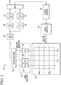
- FIG. 1 is a block diagram of a non-volatile flip flop system 100 in accordance with selected embodiments of the invention that includes non-volatile resistive memory cell array 102, read circuitry 104, error correction code (ECC) and/or redundancy decoder 106, bank select decoder 108, one or more flip flop circuitry banks 110, 112, 114, 116, multiplexer 118, ECC and/or redundancy encoder 120, and write circuitry 122.
- ECC error correction code
- 106 bank select decoder 108
- Each of a plurality of bit lines BL 1 through BL K are coupled between a corresponding column of resistive NVM cells (not shown) in NVM cell array 102 and sense amplifiers 124, 126, 128 in read circuitry 104.
- Read circuitry 104 provides a restore enable signal and sense data to an optional ECC/redundancy decoder 106.
- An indicator or address BS 0 , ...BS P of a selected bank of flip flop circuits 110-116 can also be provided to ECC and/or redundancy decoder 106 and bank select decoder 108. If ECC and/or parity bits (also referred to as "error correction bits") are added to the sensed data, the error correction bits and the sensed data are provided to bank select decoder 108. Otherwise, just the sensed data and the bank select indicator or address (BS 0 , ...BS P ) can be provided to bank select decoder 108 if ECC and/or parity decoder 106 is not included.
- ECC techniques can be used including single bit error correction methods, such as Hamming code, double bit error correction methods, such as Bose-Chaudhuri-Hocquenghem (BCH) code, or other suitable method.
- single bit error correction methods such as Hamming code
- double bit error correction methods such as Bose-Chaudhuri-Hocquenghem (BCH) code
- BCH Bose-Chaudhuri-Hocquenghem
- Sense amplifiers 124, 126, 128 in read circuitry 104 are each coupled to a respective one of bit lines BL 1 ,...BL K .
- Bank select decoder 108 receives sensed data and ECC/redundancy bits (if ECC or parity is being used), along with a bank select indicator BS 0 ,...BS P and restores the data to the selected flip flop bank 110-116.
- Multiplexer 118 is coupled to receive data from a selected one of flip flop banks 110-116 and, if error correction is being used, provide the data to ECC/redundancy encoder 120, which adds error correction bits to the data from the selected flip flop bank 110-116.
- the encoded data and ECC information is provided to write circuitry 122 along with the bank select indicator BS 0 ,...BS P . Otherwise, data from multiplexer 118 and the bank select indicator BS 0 ,...BS P can be provided directly to write circuitry 122 if error correction bits are not being used.
- Write circuitry 122 is configured to write the received data into the selected bank or set of resistive memory cells and the generated error corrections bits to resistive memory cells allocated for error correction bits.
- Write circuitry 122 can provide the data from the selected flip flop bank 110-116 along with voltages on source lines (not shown) coupled to the NVM cells, and a write enable indicator, to write the data to the selected bank of NVM cells in NVM array 102 that correspond to the selected flip flop bank 110-116.
- additional NVM cells are provided in array 102 to store the error correction bits along with the data from the flip flop circuits.
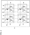
- FIG. 2 is a schematic diagram of a portion of NVM array 102 of NVM cells 202, 204, 206, 208 that can be used in the NVM flip flop system 100 of FIG. 1 .
- NVM cell 202 includes pass transistor 210 and programmable resistive elements 212, 214.
- Pass transistor 210 includes a first current electrode coupled to a first bit line BL1, a second current electrode coupled to first terminals of resistive elements 212, 214, and a gate electrode coupled to a first bank select signal BS 0 .
- a second terminal of resistive element 212 is coupled to a first source line SL1a0, and a second terminal of resistive element 214 is coupled to a first complementary source line SL1b0, that is a complement of first source line SL1a0.
- NVM cell 204 includes pass transistor 216 and programmable resistive elements 218, 220.
- Pass transistor 216 includes a first current electrode coupled to a second bit line BL2, a second current electrode coupled to first terminals of resistive elements 218, 220, and a gate electrode coupled to the first bank select signal BS 0 .
- a second terminal of resistive element 218 is coupled to a second source line SL2a0, and a second terminal of resistive element 220 is coupled to a second complementary source line SL2b0, that is a complement of second source line SL2a0.
- NVM cell 206 includes pass transistor 222 and programmable resistive elements 224, 226.
- Pass transistor 222 includes a first current electrode coupled to a first bit line BL1, a second current electrode coupled to first terminals of resistive elements 224, 226, and a gate electrode coupled to a second bank select signal BS P .
- a second terminal of resistive element 224 is coupled to a third source line SL1 ap
- a second terminal of resistive element 226 is coupled to a third complementary source line SL1 bp, that is a complement of third source line SL1ap.
- NVM cell 208 includes pass transistor 228 and programmable resistive elements 230, 232.
- Pass transistor 228 includes a first current electrode coupled to a second bit line BL2, a second current electrode coupled to first terminals of resistive elements 230, 232, and a gate electrode coupled to the second bank select signal BS P .
- a second terminal of resistive element 230 is coupled to a fourth source line SL2ap
- a second terminal of resistive element 232 is coupled to a fourth complementary source line SL2bp, that is a complement of second source line SL2ap.
- the bank select signals BS 0 , BS P can be set by a controller (not shown), or by read circuitry 104 during read or restore operations, or by write circuitry 122 during store or write operations.
- Programmable resistive elements 212, 214, 218, 220, 224, 226, 230, 232 can be implemented using magnetic tunnel junction resistors or other suitable resistive elements capable of retaining their programmed state without requiring power.
- FIG. 3 is a schematic diagram of read circuitry 104 coupled to NVM cell 202 that can be used in the NVM flip flop system 100 of FIG. 1 .
- Read circuitry 104 includes N-channel transistors 302, 304, 306, 308 and sense amplifier 124.
- N-channel transistor 302 has a first current electrode coupled to complementary source line SL1b0, a second current electrode coupled to supply voltage Vss, and a gate electrode coupled to calibration enable signal CAL.
- N-channel transistor 304 includes a first current electrode coupled to complementary source line SL1b0, a second current electrode coupled to read voltage Vread, and a gate electrode coupled to sense enable signal SENSE.
- N-channel transistor 306 includes a first current electrode coupled to source line SL1a0, a second current electrode coupled to read voltage Vread, and a control electrode coupled to the calibration enable signal CAL.
- N-channel transistor 308 includes a first current electrode coupled to source line SL1a0, a second current electrode coupled to supply voltage Vss, and a gate electrode coupled to the sense enable signal SENSE.
- Sense amplifier 124 includes a first capacitor 310 with a first terminal coupled to bit line BL1 and a second terminal coupled to an input to inverting amplifier 314.
- An output of inverting amplifier 314 is coupled to a first terminal of capacitor 316, and a second terminal of capacitor is coupled to an input of inverting amplifier 320.
- inverting amplifiers 314 and 320 may be implemented as logic inverters, or more generally could be any circuit providing negative voltage gain.
- An output of inverting amplifier 320 is data sensed on bit line BL1.
- the output of inverting amplifier 314 is coupled to a first terminal of transmission gate 312.
- a second terminal of transmission gate 312 is coupled to the input of inverting amplifier 314.
- N-channel transistor 322 includes a first current electrode coupled to the input to inverting amplifier 314, a second current electrode coupled to ground, and a control electrode coupled to RESTOREB, which is a complement of a restore enable signal.
- RESTOREB is asserted to transfer data from NVM cells in array 102 to a respective bank of flip flop circuits 110-116.
- N-channel transistor 324 includes a first current electrode coupled to the input to inverting amplifier 320, a second current electrode coupled to ground and the second current electrode of transistor 322, and a gate electrode coupled to RESTOREB.
- pass transistor 210 includes a first current electrode coupled to bit line BL1, a second current electrode coupled to first terminals of resistive elements 214, 212, and a gate electrode coupled to bank select signal BS 0 .
- a second terminal of resistive element 212 is coupled to source line SL1a0, and a second terminal of resistive element 214 is coupled to complementary source line SL1b0.
- Each row of NVM cells can be used to backup and restore a bank or group of flip flop circuits.
- the number of NVM cells in a row can be equal to the number of flip flop circuits, and a corresponding error correction bits required for each of the flip flop circuits if error correction techniques are being used.
- FIG. 4 illustrates a timing diagram of examples of store and restore operations.
- bank select BS0, calibration enable CAL, and sense enable SENSE signals are low.
- Data input DATA_IN, write enable, and the RESTOREB signals are high.
- the sensed data signal is low.
- the source line signal SL1a0 is high and the complement of the source line signal SL1b0 and the bit line signals are low.
- the state of resistive element 214 changes from high resistance to low resistance, and the state of resistive element 212 changes from low resistance to high resistance.
- bank select signal BS0 and calibration enable signal CAL are high to enter a calibration phase in which SL1a0 is biased at Vread while the SL1 b0 is biased at Vss.
- the voltage at the second current electrode of transistor 210 is thus biased at a level VCAL, which is equal to Vread* (R214/(R214+R212)), where R denotes the term "resistive element”). Since transistor 210 is ON, the voltage VCAL appears on BL1 as an input to the sense amplifier 124.
- the sense enable signal SENSE is ON and the calibration enable signal CAL is OFF.
- the inverting amplifiers 314 and 320 are connected in unity gain mode (with transmission switches 312 and 318 being ON) and thus any sense circuit voltage offsets are captured during the calibration phase in the capacitors 310 and 316.
- SL1a0 is biased at Vss while the SL1b0 is biased at Vread.
- the transmission switches 312 and 318 are OFF and the voltage at the output (SENSE_DATA) of the sense amp is proportional to (VSENSE-VCAL)
- the sense enable SENSE and sensed data signals are initially low and transition high after the calibration enable CAL signal goes low.
- Data input DATA_IN, write enable, and the complement of the restore enable RESTOREB signals are low.
- Resistive element 214 is at a low resistance state, and resistive element 212 is in a high resistance state.
- bank select BS0 To store data representing a "0" from a flip flop circuit to NVM cell 202, bank select BS0, calibration enable CAL, sense enable SENSE, and data input DATA_IN signals are low. Write enable, and the complement of the restore enable RESTOREB signals are high.
- the sensed data signal SENSE_DATA is low.
- the source line signal SL1a0 is low
- the complement of the source line signal SL1b0 is high
- bit line signal BL1 Low.
- Resistance of resistive element 214 increases while resistance of resistive element 212 decreases.
- bank select signal BS0 and calibration enable signal CAL are high to enter the calibration phase as described hereinabove.
- the sense enable signal SENSE is initially low and transitions high after the calibration enable CAL signal goes low.
- Data input DATA_IN, write enable, the complement of the restore enable RESTOREB and the sensed data SENSE_DATA signals are low.
- Resistive element 214 is at a high resistance state, and resistive element 212 is in a low resistance state.
- Control signals such as bank select, restore enable, write enable, calibration enable, sense enable, source line, and bit line signals, can be generated by a controller and/or within read circuitry 104 and/or write circuitry 122.
- NVM cells in array 102 can be written in parallel using the source lines SL1a0, SL1b0, SL2a0, SL2b0, SL1ap, SL1bp, SL2ap, SL2bp, and so on, associated with each row.
- sense amplifiers 124-128 being connected to each bit line, NVM cells in array 102 can be read in parallel, thus requiring the same amount of time to read and write independent of the number of NVM cells in each bank.
- an integrated circuit that can comprise a first plurality of flip flops, and a first bank of resistive memory cells.
- Each flip flop of the first plurality of flip flops uniquely corresponds to a resistive memory cell of the first bank of resistive memory cells.
- Write circuitry can be configured to store data from the first plurality of flip flops to the first bank of resistive memory cells.
- Read circuitry can be configured to read data from the first bank of resistive memory cells and provide the data from the first bank for storage into the first plurality of flip flops.
- the integrated circuity can further include a second plurality of flip flops; and a second bank of resistive memory cells, wherein each flip flop of the second plurality of flip flops uniquely corresponds to a resistive memory cell of the second bank of resistive memory cells, wherein the write circuitry is configured to store data from the second plurality of flips flops to the second bank of resistive memory cells, and wherein the read circuitry is configured to read data from the second bank of resistive memory cells and provide the data from the second bank for storage into the second plurality of flip flops.
- each resistive memory cell of the first bank is coupled to a first bank select line and each resistive memory cell of the second bank is coupled to a second bank select line.
- the integrated circuity can further include a bank select decoder coupled to the first and second plurality of flip flops, wherein the bank select decoder is configured to select the first plurality of flip flops when the first bank select line is asserted and the second plurality of flip flops when the second bank select line is asserted.
- the first bank of resistive memory cells includes a plurality of bit lines in which a corresponding bit line of the plurality of bit lines is coupled to each resistive memory cell of the first bank of resistive memory cells, wherein the read circuitry comprises a plurality of sense amplifiers, wherein each sense amplifier of the plurality of sense amplifiers is coupled to a corresponding bit line of the plurality of bit lines.
- the first bank of resistive memory cells includes a plurality of first source lines and a plurality of second source lines in which a corresponding first source line and a corresponding second source line is coupled to each resistive memory cell, and wherein each resistive memory cell of the first bank of resistive memory cells includes a first programmable resistive element coupled between the corresponding first source line and a corresponding internal node and a second programmable resistive element coupled between the corresponding second source line and the corresponding internal node.
- the sense amplifiers are configured to perform differential sensing when reading the data from the first bank of resistive memory cells.
- each resistive memory cell of the first bank includes a corresponding select transistor having a first current electrode coupled to the corresponding bit line, a second current electrode coupled to the corresponding internal node, and a control electrode coupled to receive a corresponding bank select line.
- the first bank of resistive memory cells includes a first set of resistive memory cells configured to store data bits and a second set of resistive memory cells configured to store error correction bits, wherein a number of resistive cells configured to store data bits equals a number of flip flops in the first plurality of flip flops.
- the integrated circuity can further include a decoder, configured to receive the data bits from the first set and the error correction bits from the second set during a read of the first bank and using the error correction bits to determine if an error in the data bits exists.
- a decoder configured to receive the data bits from the first set and the error correction bits from the second set during a read of the first bank and using the error correction bits to determine if an error in the data bits exists.
- the integrated circuity can further include an encoder, configured to receive data from the first plurality of flip flops and generate error correction bits corresponding to the received data, wherein the write circuitry, during a write to the first bank, is configured to write the received data into the first set of resistive memory cells and the generated error corrections bits to the second set of resistive memory cells.
- an encoder configured to receive data from the first plurality of flip flops and generate error correction bits corresponding to the received data
- the write circuitry during a write to the first bank, is configured to write the received data into the first set of resistive memory cells and the generated error corrections bits to the second set of resistive memory cells.
- the read circuitry is configured to read the data from the first bank in parallel and the write circuitry if configured to store the data to the first plurality of flip flops in parallel.
- an integrated circuit can comprise a plurality of flip flop banks.
- Each flip flop bank can include a plurality of flip flops and is coupled to receive a flip flop bank select indicator.
- Each of a plurality of resistive memory cell banks can correspond uniquely with a flip flop bank and can be coupled to receive a resistive memory cell bank select indicator.
- the plurality of resistive memory cell banks can include a plurality of bit lines in which each bit line of the plurality of bit lines can be coupled to a corresponding resistive memory cell of each resistive memory cell bank.
- Write circuitry can be configured to store data from a selected flip flop bank indicated by the flip bank select indicator to a selected resistive memory cell bank indicated by the resistive memory cell bank indicator.
- Read circuitry can be configured to read data from the selected resistive memory cell bank and provide the data from the selected resistive memory cell bank for storage into the selected flip flop bank.
- the read circuitry can comprise a plurality of sense amplifiers, wherein each sense amplifier of the plurality of sense amplifiers can be coupled to a corresponding bit line of the plurality of bit lines.
- each resistive memory cell bank of the plurality of resistive memory banks includes a first set of resistive memory cells configured to store data bits and a second set of resistive memory cells configured to store error correction bits, wherein a number of resistive memory cells configured to store data bits in each resistive memory cell equals a number of flip flops in each flip flop bank.
- the integrated circuity can further include a decoder, configured to the receive the data bits from the first set of resistive memory cells and the error correction bits from the second set of resistive memory cells during a read of the selected resistive memory cell bank and using the error correction bits to determine if an error in the data bits exists.
- a decoder configured to the receive the data bits from the first set of resistive memory cells and the error correction bits from the second set of resistive memory cells during a read of the selected resistive memory cell bank and using the error correction bits to determine if an error in the data bits exists.
- the integrated circuity can further include an encoder, configured to receive the data from the selected flip flop bank and generate error correction bits corresponding to the received data, wherein the write circuitry, during a write to the selected resistive memory bank, is configured to store the received data into the first set of resistive memory cells of the selected resistive memory bank and the generated error corrections bits to the second set of resistive memory cells of the selected resistive memory bank.
- an encoder configured to receive the data from the selected flip flop bank and generate error correction bits corresponding to the received data
- the write circuitry during a write to the selected resistive memory bank, is configured to store the received data into the first set of resistive memory cells of the selected resistive memory bank and the generated error corrections bits to the second set of resistive memory cells of the selected resistive memory bank.
- a method can include in response to initiating a power down, storing data bits from a first plurality of flip flops to a first bank of resistive memory cells, wherein each flip flop uniquely corresponds to a resistive memory cell; and in response to powering up, restoring the data bits from the first bank of resistive memory cells to the plurality of flip flops.
- the method can further include, during the restoring the data bits, using a corresponding sense amplifier for each bit line of the first bank of resistive memory cells to sense the data bits.
- the method can further include, during the restoring the data bits, reading error correction bits from the first bank of resistive memory cells in addition to the data bits and using the error correction bits to determine if there is an error in the data bits.
- FIG. 1 and the discussion thereof describe an exemplary information processing architecture
- this exemplary architecture is presented merely to provide a useful reference in discussing various aspects of the disclosure.
- the description of the architecture has been simplified for purposes of discussion, and it is just one of many different types of appropriate architectures that may be used in accordance with the disclosure.
- Those skilled in the art will recognize that the boundaries between logic blocks are merely illustrative and that alternative embodiments may merge logic blocks or circuit elements or impose an alternate decomposition of functionality upon various logic blocks or circuit elements.
- Coupled is not intended to be limited to a direct coupling or a mechanical coupling.
Landscapes
- Engineering & Computer Science (AREA)
- Theoretical Computer Science (AREA)
- Computer Hardware Design (AREA)
- General Engineering & Computer Science (AREA)
- General Physics & Mathematics (AREA)
- Physics & Mathematics (AREA)
- Human Computer Interaction (AREA)
- Quality & Reliability (AREA)
- Computer Security & Cryptography (AREA)
- For Increasing The Reliability Of Semiconductor Memories (AREA)
- Design And Manufacture Of Integrated Circuits (AREA)
- Semiconductor Memories (AREA)
- Read Only Memory (AREA)
- Static Random-Access Memory (AREA)
Abstract
Description
- This disclosure relates generally to flip flop circuits, and more specifically, to non-volatile flip flop circuits.
- In current systems, data in flip flop circuits is retained by supplying auxiliary backup or back-bias voltage to a portion of the flip-clop circuitry. Instead of consuming power to retain flip flop data, it is desirable to provide non-volatile flip flop circuitry that is practical to fabricate and operates efficiently under process, voltage and temperature variations.
- The present disclosure is illustrated by way of example and is not limited by the accompanying figures, in which like references indicate similar elements. Elements in the figures are illustrated for simplicity and clarity and have not necessarily been drawn to scale.
-
FIG. 1 is a block diagram of a non-volatile memory (NVM) flip flop system in accordance with selected embodiments of the invention. -
FIG. 2 is a schematic diagram of a portion of the array of NVM bit cells that can be used in the NVM flip flop system ofFIG. 1 . -
FIG. 3 is a schematic diagram of read circuitry coupled to a NVM bit cell that can be used in the NVM flip flop system ofFIG. 1 . -
FIG. 4 is a timing diagram showing examples of store and restore operations for the NVM flip flop system ofFIG. 1 . - Resistive non-volatile memory is used to provide non-volatile flip flop circuitry. Each non-volatile memory cell includes two programmable resistive elements so that data for the flip flop circuitry can be written and read differentially, providing greater accuracy. Data can be read and written in parallel. Read and write time is thus independent of the number of cells being read or written. In addition, resistive non-volatile memory (NVM) cells for storing error correction codes (ECC) and/or parity for each flip-flip circuit can be included. Sense amplifiers are coupled to each bit line to allow all NVM cells associated with a bank of flip flop circuits to be read in parallel. Multiple banks of flip flop circuits can be provided with corresponding NVM cells. The NVM cells are configured in an array and sensed using differential sensing techniques. Very little power is required to retain the state of the flip flop circuits due to the use of the programmable resistive elements, providing an ultra-low power solution for retaining the state of the flip flop circuitry.
-
FIG. 1 is a block diagram of a non-volatileflip flop system 100 in accordance with selected embodiments of the invention that includes non-volatile resistivememory cell array 102, readcircuitry 104, error correction code (ECC) and/orredundancy decoder 106,bank select decoder 108, one or more flipflop circuitry banks multiplexer 118, ECC and/orredundancy encoder 120, and writecircuitry 122. Each of a plurality of bit lines BL1 through BLK are coupled between a corresponding column of resistive NVM cells (not shown) inNVM cell array 102 andsense amplifiers read circuitry 104. Readcircuitry 104 provides a restore enable signal and sense data to an optional ECC/redundancy decoder 106. An indicator or address BS0, ...BSP of a selected bank of flip flop circuits 110-116 can also be provided to ECC and/orredundancy decoder 106 andbank select decoder 108. If ECC and/or parity bits (also referred to as "error correction bits") are added to the sensed data, the error correction bits and the sensed data are provided tobank select decoder 108. Otherwise, just the sensed data and the bank select indicator or address (BS0, ...BSP) can be provided tobank select decoder 108 if ECC and/orparity decoder 106 is not included. - Various types of ECC techniques can be used including single bit error correction methods, such as Hamming code, double bit error correction methods, such as Bose-Chaudhuri-Hocquenghem (BCH) code, or other suitable method. The inventive concepts described herein are not limited to any particular number of flip flop circuits or error correction, redundancy or parity method.
-
Sense amplifiers read circuitry 104 are each coupled to a respective one of bit lines BL1,...BLK.Bank select decoder 108 receives sensed data and ECC/redundancy bits (if ECC or parity is being used), along with a bank select indicator BS0,...BSP and restores the data to the selected flip flop bank 110-116.Multiplexer 118 is coupled to receive data from a selected one of flip flop banks 110-116 and, if error correction is being used, provide the data to ECC/redundancy encoder 120, which adds error correction bits to the data from the selected flip flop bank 110-116. The encoded data and ECC information is provided to writecircuitry 122 along with the bank select indicator BS0,...BSP. Otherwise, data frommultiplexer 118 and the bank select indicator BS0,...BSP can be provided directly to writecircuitry 122 if error correction bits are not being used.Write circuitry 122 is configured to write the received data into the selected bank or set of resistive memory cells and the generated error corrections bits to resistive memory cells allocated for error correction bits. -
Write circuitry 122 can provide the data from the selected flip flop bank 110-116 along with voltages on source lines (not shown) coupled to the NVM cells, and a write enable indicator, to write the data to the selected bank of NVM cells inNVM array 102 that correspond to the selected flip flop bank 110-116. Depending on the number of bits required for error correction, additional NVM cells are provided inarray 102 to store the error correction bits along with the data from the flip flop circuits. -
FIG. 2 is a schematic diagram of a portion ofNVM array 102 ofNVM cells flip flop system 100 ofFIG. 1 .NVM cell 202 includespass transistor 210 and programmableresistive elements Pass transistor 210 includes a first current electrode coupled to a first bit line BL1, a second current electrode coupled to first terminals ofresistive elements resistive element 212 is coupled to a first source line SL1a0, and a second terminal ofresistive element 214 is coupled to a first complementary source line SL1b0, that is a complement of first source line SL1a0. -
NVM cell 204 includespass transistor 216 and programmableresistive elements Pass transistor 216 includes a first current electrode coupled to a second bit line BL2, a second current electrode coupled to first terminals ofresistive elements resistive element 218 is coupled to a second source line SL2a0, and a second terminal ofresistive element 220 is coupled to a second complementary source line SL2b0, that is a complement of second source line SL2a0. -
NVM cell 206 includespass transistor 222 and programmableresistive elements Pass transistor 222 includes a first current electrode coupled to a first bit line BL1, a second current electrode coupled to first terminals ofresistive elements resistive element 224 is coupled to a third source line SL1 ap, and a second terminal ofresistive element 226 is coupled to a third complementary source line SL1 bp, that is a complement of third source line SL1ap. -
NVM cell 208 includespass transistor 228 and programmableresistive elements Pass transistor 228 includes a first current electrode coupled to a second bit line BL2, a second current electrode coupled to first terminals ofresistive elements resistive element 230 is coupled to a fourth source line SL2ap, and a second terminal ofresistive element 232 is coupled to a fourth complementary source line SL2bp, that is a complement of second source line SL2ap. - The bank select signals BS0, BSP can be set by a controller (not shown), or by read
circuitry 104 during read or restore operations, or by writecircuitry 122 during store or write operations. Programmableresistive elements -
FIG. 3 is a schematic diagram ofread circuitry 104 coupled toNVM cell 202 that can be used in the NVMflip flop system 100 ofFIG. 1 . Readcircuitry 104 includes N-channel transistors sense amplifier 124. N-channel transistor 302 has a first current electrode coupled to complementary source line SL1b0, a second current electrode coupled to supply voltage Vss, and a gate electrode coupled to calibration enable signal CAL. N-channel transistor 304 includes a first current electrode coupled to complementary source line SL1b0, a second current electrode coupled to read voltage Vread, and a gate electrode coupled to sense enable signal SENSE. N-channel transistor 306 includes a first current electrode coupled to source line SL1a0, a second current electrode coupled to read voltage Vread, and a control electrode coupled to the calibration enable signal CAL. N-channel transistor 308 includes a first current electrode coupled to source line SL1a0, a second current electrode coupled to supply voltage Vss, and a gate electrode coupled to the sense enable signal SENSE. -
Sense amplifier 124 includes afirst capacitor 310 with a first terminal coupled to bit line BL1 and a second terminal coupled to an input to invertingamplifier 314. An output of invertingamplifier 314 is coupled to a first terminal ofcapacitor 316, and a second terminal of capacitor is coupled to an input of invertingamplifier 320. invertingamplifiers amplifier 320 is data sensed on bit line BL1. The output of invertingamplifier 314 is coupled to a first terminal oftransmission gate 312. A second terminal oftransmission gate 312 is coupled to the input of invertingamplifier 314. The output of invertingamplifier 320 is the sensed data, and is also coupled to a first terminal oftransmission gate 318. A second terminal oftransmission gate 318 is coupled to the input of invertingamplifier 320. N-channel transistor 322 includes a first current electrode coupled to the input to invertingamplifier 314, a second current electrode coupled to ground, and a control electrode coupled to RESTOREB, which is a complement of a restore enable signal. The restore enable signal RESTORE is asserted to transfer data from NVM cells inarray 102 to a respective bank of flip flop circuits 110-116. N-channel transistor 324 includes a first current electrode coupled to the input to invertingamplifier 320, a second current electrode coupled to ground and the second current electrode oftransistor 322, and a gate electrode coupled to RESTOREB. - In
NVM cell 202,pass transistor 210 includes a first current electrode coupled to bit line BL1, a second current electrode coupled to first terminals ofresistive elements resistive element 212 is coupled to source line SL1a0, and a second terminal ofresistive element 214 is coupled to complementary source line SL1b0. - Each row of NVM cells can be used to backup and restore a bank or group of flip flop circuits. The number of NVM cells in a row can be equal to the number of flip flop circuits, and a corresponding error correction bits required for each of the flip flop circuits if error correction techniques are being used.
- The operation of
NVM cell 202 is now described with reference toFIGs. 1 ,2 and4. FIG. 4 illustrates a timing diagram of examples of store and restore operations. To store data representing a "1" from a flip flop circuit toNVM cell 202, bank select BS0, calibration enable CAL, and sense enable SENSE signals are low. Data input DATA_IN, write enable, and the RESTOREB signals are high. The sensed data signal is low. The source line signal SL1a0 is high and the complement of the source line signal SL1b0 and the bit line signals are low. The state ofresistive element 214 changes from high resistance to low resistance, and the state ofresistive element 212 changes from low resistance to high resistance. - To restore data representing a "1" from
NVM cell 202 to a flip flop circuit, bank select signal BS0 and calibration enable signal CAL are high to enter a calibration phase in which SL1a0 is biased at Vread while the SL1 b0 is biased at Vss. The voltage at the second current electrode oftransistor 210 is thus biased at a level VCAL, which is equal to Vread* (R214/(R214+R212)), where R denotes the term "resistive element"). Sincetransistor 210 is ON, the voltage VCAL appears on BL1 as an input to thesense amplifier 124. During the sense phase, the sense enable signal SENSE is ON and the calibration enable signal CAL is OFF. During the calibration phase, the invertingamplifiers transmission switches capacitors - During the sense phase, SL1a0 is biased at Vss while the SL1b0 is biased at Vread. The voltage at the second current electrode of
transistor 210 now gets biased to VSENSE=Vread*(R212/(R214+R212)). Also the transmission switches 312 and 318 are OFF and the voltage at the output (SENSE_DATA) of the sense amp is proportional to (VSENSE-VCAL) The sense enable SENSE and sensed data signals are initially low and transition high after the calibration enable CAL signal goes low. Data input DATA_IN, write enable, and the complement of the restore enable RESTOREB signals are low.Resistive element 214 is at a low resistance state, andresistive element 212 is in a high resistance state. - To store data representing a "0" from a flip flop circuit to
NVM cell 202, bank select BS0, calibration enable CAL, sense enable SENSE, and data input DATA_IN signals are low. Write enable, and the complement of the restore enable RESTOREB signals are high. The sensed data signal SENSE_DATA is low. The source line signal SL1a0 is low, the complement of the source line signal SL1b0 is high, and the bit line signal BL1 is low. Resistance ofresistive element 214 increases while resistance ofresistive element 212 decreases. - To restore data representing a "0" from
NVM cell 202 to a flip flop circuit, bank select signal BS0 and calibration enable signal CAL are high to enter the calibration phase as described hereinabove. The sense enable signal SENSE is initially low and transitions high after the calibration enable CAL signal goes low. Data input DATA_IN, write enable, the complement of the restore enable RESTOREB and the sensed data SENSE_DATA signals are low.Resistive element 214 is at a high resistance state, andresistive element 212 is in a low resistance state. - Control signals such as bank select, restore enable, write enable, calibration enable, sense enable, source line, and bit line signals, can be generated by a controller and/or within
read circuitry 104 and/or writecircuitry 122. NVM cells inarray 102 can be written in parallel using the source lines SL1a0, SL1b0, SL2a0, SL2b0, SL1ap, SL1bp, SL2ap, SL2bp, and so on, associated with each row. Similarly, with sense amplifiers 124-128 being connected to each bit line, NVM cells inarray 102 can be read in parallel, thus requiring the same amount of time to read and write independent of the number of NVM cells in each bank. - By now it should be appreciated that in selected embodiments, there has been provided an integrated circuit that can comprise a first plurality of flip flops, and a first bank of resistive memory cells. Each flip flop of the first plurality of flip flops uniquely corresponds to a resistive memory cell of the first bank of resistive memory cells. Write circuitry can be configured to store data from the first plurality of flip flops to the first bank of resistive memory cells. Read circuitry can be configured to read data from the first bank of resistive memory cells and provide the data from the first bank for storage into the first plurality of flip flops.
- In another aspect, the integrated circuity can further include a second plurality of flip flops; and a second bank of resistive memory cells, wherein each flip flop of the second plurality of flip flops uniquely corresponds to a resistive memory cell of the second bank of resistive memory cells, wherein the write circuitry is configured to store data from the second plurality of flips flops to the second bank of resistive memory cells, and wherein the read circuitry is configured to read data from the second bank of resistive memory cells and provide the data from the second bank for storage into the second plurality of flip flops.
- In another aspect, each resistive memory cell of the first bank is coupled to a first bank select line and each resistive memory cell of the second bank is coupled to a second bank select line.
- In another aspect, the integrated circuity can further include a bank select decoder coupled to the first and second plurality of flip flops, wherein the bank select decoder is configured to select the first plurality of flip flops when the first bank select line is asserted and the second plurality of flip flops when the second bank select line is asserted.
- In another aspect, the first bank of resistive memory cells includes a plurality of bit lines in which a corresponding bit line of the plurality of bit lines is coupled to each resistive memory cell of the first bank of resistive memory cells, wherein the read circuitry comprises a plurality of sense amplifiers, wherein each sense amplifier of the plurality of sense amplifiers is coupled to a corresponding bit line of the plurality of bit lines.
- In another aspect, the first bank of resistive memory cells includes a plurality of first source lines and a plurality of second source lines in which a corresponding first source line and a corresponding second source line is coupled to each resistive memory cell, and wherein each resistive memory cell of the first bank of resistive memory cells includes a first programmable resistive element coupled between the corresponding first source line and a corresponding internal node and a second programmable resistive element coupled between the corresponding second source line and the corresponding internal node.
- In another aspect, the sense amplifiers are configured to perform differential sensing when reading the data from the first bank of resistive memory cells.
- In another aspect, each resistive memory cell of the first bank includes a corresponding select transistor having a first current electrode coupled to the corresponding bit line, a second current electrode coupled to the corresponding internal node, and a control electrode coupled to receive a corresponding bank select line.
- In another aspect, the first bank of resistive memory cells includes a first set of resistive memory cells configured to store data bits and a second set of resistive memory cells configured to store error correction bits, wherein a number of resistive cells configured to store data bits equals a number of flip flops in the first plurality of flip flops.
- In another aspect, the integrated circuity can further include a decoder, configured to receive the data bits from the first set and the error correction bits from the second set during a read of the first bank and using the error correction bits to determine if an error in the data bits exists.
- In another aspect, the integrated circuity can further include an encoder, configured to receive data from the first plurality of flip flops and generate error correction bits corresponding to the received data, wherein the write circuitry, during a write to the first bank, is configured to write the received data into the first set of resistive memory cells and the generated error corrections bits to the second set of resistive memory cells.
- In another aspect, the read circuitry is configured to read the data from the first bank in parallel and the write circuitry if configured to store the data to the first plurality of flip flops in parallel.
- In other selected embodiments, an integrated circuit can comprise a plurality of flip flop banks. Each flip flop bank can include a plurality of flip flops and is coupled to receive a flip flop bank select indicator. Each of a plurality of resistive memory cell banks can correspond uniquely with a flip flop bank and can be coupled to receive a resistive memory cell bank select indicator. The plurality of resistive memory cell banks can include a plurality of bit lines in which each bit line of the plurality of bit lines can be coupled to a corresponding resistive memory cell of each resistive memory cell bank. Write circuitry can be configured to store data from a selected flip flop bank indicated by the flip bank select indicator to a selected resistive memory cell bank indicated by the resistive memory cell bank indicator. Read circuitry can be configured to read data from the selected resistive memory cell bank and provide the data from the selected resistive memory cell bank for storage into the selected flip flop bank.
- In another aspect, the read circuitry can comprise a plurality of sense amplifiers, wherein each sense amplifier of the plurality of sense amplifiers can be coupled to a corresponding bit line of the plurality of bit lines.
- In another aspect, each resistive memory cell bank of the plurality of resistive memory banks includes a first set of resistive memory cells configured to store data bits and a second set of resistive memory cells configured to store error correction bits, wherein a number of resistive memory cells configured to store data bits in each resistive memory cell equals a number of flip flops in each flip flop bank.
- In another aspect, the integrated circuity can further include a decoder, configured to the receive the data bits from the first set of resistive memory cells and the error correction bits from the second set of resistive memory cells during a read of the selected resistive memory cell bank and using the error correction bits to determine if an error in the data bits exists.
- In another aspect, the integrated circuity can further include an encoder, configured to receive the data from the selected flip flop bank and generate error correction bits corresponding to the received data, wherein the write circuitry, during a write to the selected resistive memory bank, is configured to store the received data into the first set of resistive memory cells of the selected resistive memory bank and the generated error corrections bits to the second set of resistive memory cells of the selected resistive memory bank.
- In still further selected embodiments, a method can include in response to initiating a power down, storing data bits from a first plurality of flip flops to a first bank of resistive memory cells, wherein each flip flop uniquely corresponds to a resistive memory cell; and in response to powering up, restoring the data bits from the first bank of resistive memory cells to the plurality of flip flops.
- In another aspect, the method can further include, during the restoring the data bits, using a corresponding sense amplifier for each bit line of the first bank of resistive memory cells to sense the data bits.
- In another aspect, the method can further include, during the restoring the data bits, reading error correction bits from the first bank of resistive memory cells in addition to the data bits and using the error correction bits to determine if there is an error in the data bits.
- Because the apparatus implementing the present disclosure is, for the most part, composed of electronic components and circuits known to those skilled in the art, circuit details will not be explained in any greater extent than that considered necessary as illustrated above, for the understanding and appreciation of the underlying concepts of the present disclosure and in order not to obfuscate or distract from the teachings of the present disclosure.
- Although the disclosure has been described with respect to specific conductivity types or polarity of potentials, skilled artisans appreciated that conductivity types and polarities of potentials may be reversed.
- Moreover, the terms "front," "back," "top," "bottom," "over," "under" and the like in the description and in the claims, if any, are used for descriptive purposes and not necessarily for describing permanent relative positions. It is understood that the terms so used are interchangeable under appropriate circumstances such that the embodiments of the disclosure described herein are, for example, capable of operation in other orientations than those illustrated or otherwise described herein.
- Some of the above embodiments, as applicable, may be implemented using a variety of different information processing systems. For example, although
FIG. 1 and the discussion thereof describe an exemplary information processing architecture, this exemplary architecture is presented merely to provide a useful reference in discussing various aspects of the disclosure. Of course, the description of the architecture has been simplified for purposes of discussion, and it is just one of many different types of appropriate architectures that may be used in accordance with the disclosure. Those skilled in the art will recognize that the boundaries between logic blocks are merely illustrative and that alternative embodiments may merge logic blocks or circuit elements or impose an alternate decomposition of functionality upon various logic blocks or circuit elements. - Although the disclosure is described herein with reference to specific embodiments, various modifications and changes can be made without departing from the scope of the present disclosure as set forth in the claims below. Accordingly, the specification and figures are to be regarded in an illustrative rather than a restrictive sense, and all such modifications are intended to be included within the scope of the present disclosure. Any benefits, advantages, or solutions to problems that are described herein with regard to specific embodiments are not intended to be construed as a critical, required, or essential feature or element of any or all the claims.
- The term "coupled," as used herein, is not intended to be limited to a direct coupling or a mechanical coupling.
- Furthermore, the terms "a" or "an," as used herein, are defined as one or more than one. Also, the use of introductory phrases such as "at least one" and "one or more" in the claims should not be construed to imply that the introduction of another claim element by the indefinite articles "a" or "an" limits any particular claim containing such introduced claim element to disclosures containing only one such element, even when the same claim includes the introductory phrases "one or more" or "at least one" and indefinite articles such as "a" or "an." The same holds true for the use of definite articles.
- Unless stated otherwise, terms such as "first" and "second" are used to arbitrarily distinguish between the elements such terms describe. Thus, these terms are not necessarily intended to indicate temporal or other prioritization of such elements.
Claims (15)
- An integrated circuit, comprising:a first plurality of flip flops (110, 112);a first bank of resistive memory cells (202, 204), wherein each flip flop of the first plurality of flip flops (110, 112) uniquely corresponds to a resistive memory cell of the first bank of resistive memory cells (202, 204);write circuitry (122) configured to store data from the first plurality of flip flops (110, 112) to the first bank of resistive memory cells (202, 204); andread circuitry (104) configured to read data from the first bank of resistive memory cells (202, 204) and provide the data from the first bank for storage into the first plurality of flip flops (110, 112).
- The integrated circuity of claim 1, further comprising:a second plurality of flip flops (114, 116); anda second bank of resistive memory cells (206, 208), wherein each flip flop of the second plurality of flip flops (114, 116) uniquely corresponds to a resistive memory cell of the second bank of resistive memory cells (206, 208), wherein the write circuitry (122) is configured to store data from the second plurality of flips flops to the second bank of resistive memory cells (206, 208), and wherein the read circuitry (104) is configured to read data from the second bank of resistive memory cells (206, 208) and provide the data from the second bank for storage into the second plurality of flip flops (114, 116).
- The integrated circuit of claim 2, wherein each resistive memory cell of the first bank is coupled to a first bank select line (BSo) and each resistive memory cell of the second bank is coupled to a second bank select line (BSP), wherein the integrated circuit further comprises a bank select decoder (108) coupled to the first and second plurality of flip flops (110 - 116), wherein the bank select decoder (108) is configured to select the first plurality of flip flops (110, 112) when the first bank select line (BS0) is asserted and the second plurality of flip flops (114, 116) when the second bank select line (BSP) is asserted.
- The integrated circuit of any one of the claims 1 to 3, wherein the first bank of resistive memory cells (202, 204) includes a plurality of bit lines (BL1 - BLK) in which a corresponding bit line of the plurality of bit lines (BL1 - BLK) is coupled to each resistive memory cell of the first bank of resistive memory cells (202, 204), wherein the read circuitry (104) comprises:a plurality of sense amplifiers (124 - 128), wherein each sense amplifier of the plurality of sense amplifiers (124 - 128) is coupled to a corresponding bit line of the plurality of bit lines (BL1 - BLK).
- The integrated circuit of claim 4, wherein the first bank of resistive memory cells (202, 204) includes a plurality of first source lines (SL1a0 - SL1ap) and a plurality of second source lines (SL1b0 - SL1 bp) in which a corresponding first source line and a corresponding second source line is coupled to each resistive memory cell, and wherein each resistive memory cell of the first bank of resistive memory cells (202, 204) includes a first programmable resistive element (212, 218) coupled between the corresponding first source line (SL1a0, SL2a0) and a corresponding internal node and a second programmable resistive element (214, 220) coupled between the corresponding second source line (SL1b0. SL2b0) and the corresponding internal node.
- The integrated circuit of claim 5, wherein each resistive memory cell of the first bank includes a corresponding select transistor (210, 216) having a first current electrode coupled to the corresponding bit line (B1, BL2), a second current electrode coupled to the corresponding internal node, and a control electrode coupled to receive a corresponding bank select line.
- The integrated circuit of any one of the claims 1 to 6, wherein the first bank of resistive memory cells (202, 204) includes a first set of resistive memory cells configured to store data bits and a second set of resistive memory cells configured to store error correction bits, wherein a number of resistive cells configured to store data bits equals a number of flip flops in the first plurality of flip flops (110, 112).
- The integrated circuit of claim 7, further comprising at least one of:a decoder (106), configured to the receive the data bits from the first set and the error correction bits from the second set during a read of the first bank and using the error correction bits to determine if an error in the data bits exists; andan encoder (120), configured to receive data from the first plurality of flip flops (110, 112) and generate error correction bits corresponding to the received data, wherein the write circuitry (122), during a write to the first bank, is configured to write the received data into the first set of resistive memory cells and the generated error corrections bits to the second set of resistive memory cells.
- An integrated circuit, comprising:a plurality of flip flop banks (110 - 116), wherein each flip flop bank includes a plurality of flip flops and is coupled to receive a flip flop bank select indicator;a plurality of resistive memory cell banks, wherein each of the resistive memory cell banks corresponds uniquely with a flip flop bank and is coupled to receive a resistive memory cell bank select indicator (BS0 - BSP), wherein the plurality of resistive memory cell banks includes a plurality of bit lines (BL1 - BLK) in which each bit line of the plurality of bit lines (BL1 - BLK) is coupled to a corresponding resistive memory cell (202 - 208) of each resistive memory cell bank;write circuitry (122) configured to store data from a selected flip flop bank indicated by the flip bank select indicator to a selected resistive memory cell bank indicated by the resistive memory cell bank indicator; andread circuitry (104) configured to read data from the selected resistive memory cell bank and provide the data from the selected resistive memory cell bank for storage into the selected flip flop bank.
- The integrated circuit of claim 9, wherein the read circuitry (104) comprises:a plurality of sense amplifiers (124 - 128), wherein each sense amplifier of the plurality of sense amplifiers (124 - 128) is coupled to a corresponding bit line of the plurality of bit lines (BL1 - BLK).
- The integrated circuit of claim 9 or claim 10, wherein each resistive memory cell bank of the plurality of resistive memory banks includes a first set of resistive memory cells configured to store data bits and a second set of resistive memory cells configured to store error correction bits, wherein a number of resistive memory cells configured to store data bits in each resistive memory cell equals a number of flip flops in each flip flop bank.
- The integrated circuit of claim 11, further comprising at least one of:a decoder (106), configured to the receive the data bits from the first set of resistive memory cells and the error correction bits from the second set of resistive memory cells during a read of the selected resistive memory cell bank and using the error correction bits to determine if an error in the data bits exists; andan encoder (120), configured to receive the data from the selected flip flop bank and generate error correction bits corresponding to the received data, wherein the write circuitry (122), during a write to the selected resistive memory bank, is configured to store the received data into the first set of resistive memory cells of the selected resistive memory bank and the generated error corrections bits to the second set of resistive memory cells of the selected resistive memory bank.
- A method, comprising:in response to initiating a power down, storing data bits from a first plurality of flip flops (110, 112) to a first bank of resistive memory cells (202, 204), wherein each flip flop uniquely corresponds to a resistive memory cell; andin response to powering up, restoring the data bits from the first bank of resistive memory cells (202, 204) to the plurality of flip flops.
- The method of claim 13, further comprising:during the restoring the data bits, using a corresponding sense amplifier for each bit line of the first bank of resistive memory cells (202, 204) to sense the data bits.
- The method of claim 13 or claim 14, further comprising:during the restoring the data bits, reading error correction bits from the first bank of resistive memory cells (202, 204) in addition to the data bits and using the error correction bits to determine if there is an error in the data bits.
Applications Claiming Priority (1)
| Application Number | Priority Date | Filing Date | Title |
|---|---|---|---|
| US15/163,801 US10297314B2 (en) | 2016-05-25 | 2016-05-25 | Systems and methods for non-volatile flip flops |
Publications (3)
| Publication Number | Publication Date |
|---|---|
| EP3249654A2 true EP3249654A2 (en) | 2017-11-29 |
| EP3249654A3 EP3249654A3 (en) | 2018-02-21 |
| EP3249654B1 EP3249654B1 (en) | 2020-10-21 |
Family
ID=58412856
Family Applications (1)
| Application Number | Title | Priority Date | Filing Date |
|---|---|---|---|
| EP17160166.9A Active EP3249654B1 (en) | 2016-05-25 | 2017-03-09 | Systems and methods for non-volatile flip flops |
Country Status (2)
| Country | Link |
|---|---|
| US (1) | US10297314B2 (en) |
| EP (1) | EP3249654B1 (en) |
Families Citing this family (2)
| Publication number | Priority date | Publication date | Assignee | Title |
|---|---|---|---|---|
| WO2018167962A1 (en) * | 2017-03-17 | 2018-09-20 | Nec Corporation | Reconfigurable circuit using nonvolatile resistive switches |
| US10916324B2 (en) * | 2018-09-11 | 2021-02-09 | Micron Technology, Inc. | Data state synchronization involving memory cells having an inverted data state written thereto |
Family Cites Families (16)
| Publication number | Priority date | Publication date | Assignee | Title |
|---|---|---|---|---|
| JPH03296993A (en) * | 1990-04-16 | 1991-12-27 | Hitachi Ltd | Semiconductor integrated circuit devices, storage devices and digital processing devices |
| JP2914870B2 (en) * | 1994-05-25 | 1999-07-05 | 株式会社東芝 | Semiconductor integrated circuit |
| US5694056A (en) * | 1996-04-01 | 1997-12-02 | Xilinx, Inc. | Fast pipeline frame full detector |
| US6606267B2 (en) * | 1998-06-23 | 2003-08-12 | Sandisk Corporation | High data rate write process for non-volatile flash memories |
| JP2001035196A (en) * | 1999-07-26 | 2001-02-09 | Mitsubishi Electric Corp | Semiconductor integrated circuit device with failure analysis function |
| US7894269B2 (en) * | 2006-07-20 | 2011-02-22 | Sandisk Corporation | Nonvolatile memory and method for compensating during programming for perturbing charges of neighboring cells |
| JP2009070474A (en) * | 2007-09-13 | 2009-04-02 | Panasonic Corp | Semiconductor integrated circuit |
| US8194492B2 (en) * | 2008-04-08 | 2012-06-05 | Samsung Electronics Co., Ltd. | Variable resistance memory device and system |
| US8416598B2 (en) * | 2009-05-21 | 2013-04-09 | Texas Instruments Incorporated | Differential plate line screen test for ferroelectric latch circuits |
| JP2010282411A (en) * | 2009-06-04 | 2010-12-16 | Renesas Electronics Corp | Semiconductor integrated circuit and method for saving and restoring internal state of semiconductor integrated circuit |
| WO2011001562A1 (en) * | 2009-06-30 | 2011-01-06 | パナソニック株式会社 | Semiconductor integrated circuit |
| TW201320079A (en) | 2011-11-08 | 2013-05-16 | Ind Tech Res Inst | Nonvolatile random access memory and operation method thereof |
| US9147464B1 (en) * | 2012-05-15 | 2015-09-29 | Adesto Technologies Corporation | System architecture with multiple memory types, including programmable impedance memory elements |
| TW201417102A (en) * | 2012-10-23 | 2014-05-01 | Ind Tech Res Inst | Resistive random-access memory devices |
| FR3008219B1 (en) * | 2013-07-05 | 2016-12-09 | Commissariat Energie Atomique | NON-VOLATILE MEMORY DEVICE |
| FR3022374B1 (en) * | 2014-06-17 | 2018-11-16 | Commissariat A L'energie Atomique Et Aux Energies Alternatives | REGISTER HAVING NON-VOLATILE MEMORY FOR SAVING AND RESTORING A VOLATILE MEMORY |
-
2016
- 2016-05-25 US US15/163,801 patent/US10297314B2/en active Active
-
2017
- 2017-03-09 EP EP17160166.9A patent/EP3249654B1/en active Active
Non-Patent Citations (1)
| Title |
|---|
| None |
Also Published As
| Publication number | Publication date |
|---|---|
| EP3249654B1 (en) | 2020-10-21 |
| US20170345491A1 (en) | 2017-11-30 |
| US10297314B2 (en) | 2019-05-21 |
| EP3249654A3 (en) | 2018-02-21 |
Similar Documents
| Publication | Publication Date | Title |
|---|---|---|
| US10522222B2 (en) | Semiconductor device and error correction method | |
| CN107437426B (en) | Nonvolatile static random access memory system and operation method | |
| CN119046055A (en) | Memory system with error correction and data scrubbing circuits | |
| US9406353B2 (en) | Sense amplifiers, memories, and apparatuses and methods for sensing a data state of a memory cell | |
| EP3244417A1 (en) | Magnetic random access memory (mram) and method of operation | |
| CN102956268A (en) | Data reading circuit, non-volatile memory device and data reading method | |
| US20170153933A1 (en) | Apparatus and method for detecting single flip-error in a complementary resistive memory | |
| US9640258B2 (en) | Ternary content addressable memory (TCAM) with magnetic tunnel junction (MTJ) devices | |
| US20180277186A1 (en) | Memory device | |
| KR20170083939A (en) | Resistive random access memory apparatus | |
| WO2020117568A1 (en) | Direct-input redundancy scheme with adaptive syndrome decoder | |
| CN112216320B (en) | Reference voltage generation for voltage sensing in resistive memory | |
| CN106997780B (en) | Sense amplifier | |
| EP2945164B1 (en) | Nonvolatile semiconductor storage device and method for testing same | |
| US9514810B1 (en) | Resistive non-volatile memory cell and method for programming same | |
| US9576661B2 (en) | Systems and methods for SRAM with backup non-volatile memory that includes MTJ resistive elements | |
| EP3457403B1 (en) | Resistive non-volatile memory and a method for sensing a memory cell in a resistive non-volatile memory | |
| US10297314B2 (en) | Systems and methods for non-volatile flip flops | |
| EP3518240B1 (en) | Resistive non-volatile memory and a method for sensing a memory cell in a resistive non-volatile memory | |
| US20170047101A1 (en) | Sensing and reference voltage scheme for random access memory | |
| US20120269009A1 (en) | Memory array with two-phase bit line precharge | |
| US9349426B1 (en) | Non-volatile random access memory (NVRAM) | |
| US20180019735A1 (en) | Systems and methods for non-volatile flip flops | |
| US11769567B2 (en) | Devices and methods for preventing errors and detecting faults within a memory device | |
| CN114203221B (en) | Semiconductor memory devices and their control methods |
Legal Events
| Date | Code | Title | Description |
|---|---|---|---|
| PUAI | Public reference made under article 153(3) epc to a published international application that has entered the european phase |
Free format text: ORIGINAL CODE: 0009012 |
|
| STAA | Information on the status of an ep patent application or granted ep patent |
Free format text: STATUS: THE APPLICATION HAS BEEN PUBLISHED |
|
| AK | Designated contracting states |
Kind code of ref document: A2 Designated state(s): AL AT BE BG CH CY CZ DE DK EE ES FI FR GB GR HR HU IE IS IT LI LT LU LV MC MK MT NL NO PL PT RO RS SE SI SK SM TR |
|
| AX | Request for extension of the european patent |
Extension state: BA ME |
|
| PUAL | Search report despatched |
Free format text: ORIGINAL CODE: 0009013 |
|
| AK | Designated contracting states |
Kind code of ref document: A3 Designated state(s): AL AT BE BG CH CY CZ DE DK EE ES FI FR GB GR HR HU IE IS IT LI LT LU LV MC MK MT NL NO PL PT RO RS SE SI SK SM TR |
|
| AX | Request for extension of the european patent |
Extension state: BA ME |
|
| RIC1 | Information provided on ipc code assigned before grant |
Ipc: G11C 13/00 20060101ALI20180112BHEP Ipc: G11C 11/16 20060101ALI20180112BHEP Ipc: G11C 11/00 20060101AFI20180112BHEP Ipc: G11C 11/22 20060101ALI20180112BHEP |
|
| STAA | Information on the status of an ep patent application or granted ep patent |
Free format text: STATUS: REQUEST FOR EXAMINATION WAS MADE |
|
| 17P | Request for examination filed |
Effective date: 20180821 |
|
| RBV | Designated contracting states (corrected) |
Designated state(s): AL AT BE BG CH CY CZ DE DK EE ES FI FR GB GR HR HU IE IS IT LI LT LU LV MC MK MT NL NO PL PT RO RS SE SI SK SM TR |
|
| GRAP | Despatch of communication of intention to grant a patent |
Free format text: ORIGINAL CODE: EPIDOSNIGR1 |
|
| STAA | Information on the status of an ep patent application or granted ep patent |
Free format text: STATUS: GRANT OF PATENT IS INTENDED |
|
| INTG | Intention to grant announced |
Effective date: 20200724 |
|
| RIN1 | Information on inventor provided before grant (corrected) |
Inventor name: ROY, ANIRBAN Inventor name: SADD, MICHAEL A. |
|
| GRAS | Grant fee paid |
Free format text: ORIGINAL CODE: EPIDOSNIGR3 |
|
| GRAA | (expected) grant |
Free format text: ORIGINAL CODE: 0009210 |
|
| STAA | Information on the status of an ep patent application or granted ep patent |
Free format text: STATUS: THE PATENT HAS BEEN GRANTED |
|
| AK | Designated contracting states |
Kind code of ref document: B1 Designated state(s): AL AT BE BG CH CY CZ DE DK EE ES FI FR GB GR HR HU IE IS IT LI LT LU LV MC MK MT NL NO PL PT RO RS SE SI SK SM TR |
|
| REG | Reference to a national code |
Ref country code: GB Ref legal event code: FG4D |
|
| REG | Reference to a national code |
Ref country code: CH Ref legal event code: EP |
|
| REG | Reference to a national code |
Ref country code: IE Ref legal event code: FG4D |
|
| REG | Reference to a national code |
Ref country code: DE Ref legal event code: R096 Ref document number: 602017025703 Country of ref document: DE |
|
| REG | Reference to a national code |
Ref country code: AT Ref legal event code: REF Ref document number: 1326660 Country of ref document: AT Kind code of ref document: T Effective date: 20201115 |
|
| REG | Reference to a national code |
Ref country code: AT Ref legal event code: MK05 Ref document number: 1326660 Country of ref document: AT Kind code of ref document: T Effective date: 20201021 |
|
| REG | Reference to a national code |
Ref country code: NL Ref legal event code: MP Effective date: 20201021 |
|
| PG25 | Lapsed in a contracting state [announced via postgrant information from national office to epo] |
Ref country code: NO Free format text: LAPSE BECAUSE OF FAILURE TO SUBMIT A TRANSLATION OF THE DESCRIPTION OR TO PAY THE FEE WITHIN THE PRESCRIBED TIME-LIMIT Effective date: 20210121 Ref country code: NL Free format text: LAPSE BECAUSE OF FAILURE TO SUBMIT A TRANSLATION OF THE DESCRIPTION OR TO PAY THE FEE WITHIN THE PRESCRIBED TIME-LIMIT Effective date: 20201021 Ref country code: RS Free format text: LAPSE BECAUSE OF FAILURE TO SUBMIT A TRANSLATION OF THE DESCRIPTION OR TO PAY THE FEE WITHIN THE PRESCRIBED TIME-LIMIT Effective date: 20201021 Ref country code: PT Free format text: LAPSE BECAUSE OF FAILURE TO SUBMIT A TRANSLATION OF THE DESCRIPTION OR TO PAY THE FEE WITHIN THE PRESCRIBED TIME-LIMIT Effective date: 20210222 Ref country code: GR Free format text: LAPSE BECAUSE OF FAILURE TO SUBMIT A TRANSLATION OF THE DESCRIPTION OR TO PAY THE FEE WITHIN THE PRESCRIBED TIME-LIMIT Effective date: 20210122 Ref country code: FI Free format text: LAPSE BECAUSE OF FAILURE TO SUBMIT A TRANSLATION OF THE DESCRIPTION OR TO PAY THE FEE WITHIN THE PRESCRIBED TIME-LIMIT Effective date: 20201021 |
|
| REG | Reference to a national code |
Ref country code: LT Ref legal event code: MG4D |
|
| PG25 | Lapsed in a contracting state [announced via postgrant information from national office to epo] |
Ref country code: ES Free format text: LAPSE BECAUSE OF FAILURE TO SUBMIT A TRANSLATION OF THE DESCRIPTION OR TO PAY THE FEE WITHIN THE PRESCRIBED TIME-LIMIT Effective date: 20201021 Ref country code: AT Free format text: LAPSE BECAUSE OF FAILURE TO SUBMIT A TRANSLATION OF THE DESCRIPTION OR TO PAY THE FEE WITHIN THE PRESCRIBED TIME-LIMIT Effective date: 20201021 Ref country code: BG Free format text: LAPSE BECAUSE OF FAILURE TO SUBMIT A TRANSLATION OF THE DESCRIPTION OR TO PAY THE FEE WITHIN THE PRESCRIBED TIME-LIMIT Effective date: 20210121 Ref country code: IS Free format text: LAPSE BECAUSE OF FAILURE TO SUBMIT A TRANSLATION OF THE DESCRIPTION OR TO PAY THE FEE WITHIN THE PRESCRIBED TIME-LIMIT Effective date: 20210221 Ref country code: LV Free format text: LAPSE BECAUSE OF FAILURE TO SUBMIT A TRANSLATION OF THE DESCRIPTION OR TO PAY THE FEE WITHIN THE PRESCRIBED TIME-LIMIT Effective date: 20201021 Ref country code: PL Free format text: LAPSE BECAUSE OF FAILURE TO SUBMIT A TRANSLATION OF THE DESCRIPTION OR TO PAY THE FEE WITHIN THE PRESCRIBED TIME-LIMIT Effective date: 20201021 Ref country code: SE Free format text: LAPSE BECAUSE OF FAILURE TO SUBMIT A TRANSLATION OF THE DESCRIPTION OR TO PAY THE FEE WITHIN THE PRESCRIBED TIME-LIMIT Effective date: 20201021 |
|
| PG25 | Lapsed in a contracting state [announced via postgrant information from national office to epo] |
Ref country code: HR Free format text: LAPSE BECAUSE OF FAILURE TO SUBMIT A TRANSLATION OF THE DESCRIPTION OR TO PAY THE FEE WITHIN THE PRESCRIBED TIME-LIMIT Effective date: 20201021 |
|
| REG | Reference to a national code |
Ref country code: DE Ref legal event code: R097 Ref document number: 602017025703 Country of ref document: DE |
|
| PG25 | Lapsed in a contracting state [announced via postgrant information from national office to epo] |
Ref country code: SK Free format text: LAPSE BECAUSE OF FAILURE TO SUBMIT A TRANSLATION OF THE DESCRIPTION OR TO PAY THE FEE WITHIN THE PRESCRIBED TIME-LIMIT Effective date: 20201021 Ref country code: RO Free format text: LAPSE BECAUSE OF FAILURE TO SUBMIT A TRANSLATION OF THE DESCRIPTION OR TO PAY THE FEE WITHIN THE PRESCRIBED TIME-LIMIT Effective date: 20201021 Ref country code: SM Free format text: LAPSE BECAUSE OF FAILURE TO SUBMIT A TRANSLATION OF THE DESCRIPTION OR TO PAY THE FEE WITHIN THE PRESCRIBED TIME-LIMIT Effective date: 20201021 Ref country code: LT Free format text: LAPSE BECAUSE OF FAILURE TO SUBMIT A TRANSLATION OF THE DESCRIPTION OR TO PAY THE FEE WITHIN THE PRESCRIBED TIME-LIMIT Effective date: 20201021 Ref country code: EE Free format text: LAPSE BECAUSE OF FAILURE TO SUBMIT A TRANSLATION OF THE DESCRIPTION OR TO PAY THE FEE WITHIN THE PRESCRIBED TIME-LIMIT Effective date: 20201021 Ref country code: CZ Free format text: LAPSE BECAUSE OF FAILURE TO SUBMIT A TRANSLATION OF THE DESCRIPTION OR TO PAY THE FEE WITHIN THE PRESCRIBED TIME-LIMIT Effective date: 20201021 |
|
| PLBE | No opposition filed within time limit |
Free format text: ORIGINAL CODE: 0009261 |
|
| STAA | Information on the status of an ep patent application or granted ep patent |
Free format text: STATUS: NO OPPOSITION FILED WITHIN TIME LIMIT |
|
| PG25 | Lapsed in a contracting state [announced via postgrant information from national office to epo] |
Ref country code: DK Free format text: LAPSE BECAUSE OF FAILURE TO SUBMIT A TRANSLATION OF THE DESCRIPTION OR TO PAY THE FEE WITHIN THE PRESCRIBED TIME-LIMIT Effective date: 20201021 |
|
| 26N | No opposition filed |
Effective date: 20210722 |
|
| PG25 | Lapsed in a contracting state [announced via postgrant information from national office to epo] |
Ref country code: AL Free format text: LAPSE BECAUSE OF FAILURE TO SUBMIT A TRANSLATION OF THE DESCRIPTION OR TO PAY THE FEE WITHIN THE PRESCRIBED TIME-LIMIT Effective date: 20201021 Ref country code: IT Free format text: LAPSE BECAUSE OF FAILURE TO SUBMIT A TRANSLATION OF THE DESCRIPTION OR TO PAY THE FEE WITHIN THE PRESCRIBED TIME-LIMIT Effective date: 20201021 Ref country code: MC Free format text: LAPSE BECAUSE OF FAILURE TO SUBMIT A TRANSLATION OF THE DESCRIPTION OR TO PAY THE FEE WITHIN THE PRESCRIBED TIME-LIMIT Effective date: 20201021 |
|
| REG | Reference to a national code |
Ref country code: CH Ref legal event code: PL |
|
| GBPC | Gb: european patent ceased through non-payment of renewal fee |
Effective date: 20210309 |
|
| PG25 | Lapsed in a contracting state [announced via postgrant information from national office to epo] |
Ref country code: SI Free format text: LAPSE BECAUSE OF FAILURE TO SUBMIT A TRANSLATION OF THE DESCRIPTION OR TO PAY THE FEE WITHIN THE PRESCRIBED TIME-LIMIT Effective date: 20201021 |
|
| REG | Reference to a national code |
Ref country code: BE Ref legal event code: MM Effective date: 20210331 |
|
| PG25 | Lapsed in a contracting state [announced via postgrant information from national office to epo] |
Ref country code: CH Free format text: LAPSE BECAUSE OF NON-PAYMENT OF DUE FEES Effective date: 20210331 Ref country code: LI Free format text: LAPSE BECAUSE OF NON-PAYMENT OF DUE FEES Effective date: 20210331 Ref country code: LU Free format text: LAPSE BECAUSE OF NON-PAYMENT OF DUE FEES Effective date: 20210309 Ref country code: FR Free format text: LAPSE BECAUSE OF NON-PAYMENT OF DUE FEES Effective date: 20210331 Ref country code: GB Free format text: LAPSE BECAUSE OF NON-PAYMENT OF DUE FEES Effective date: 20210309 Ref country code: IE Free format text: LAPSE BECAUSE OF NON-PAYMENT OF DUE FEES Effective date: 20210309 |
|
| PG25 | Lapsed in a contracting state [announced via postgrant information from national office to epo] |
Ref country code: IS Free format text: LAPSE BECAUSE OF FAILURE TO SUBMIT A TRANSLATION OF THE DESCRIPTION OR TO PAY THE FEE WITHIN THE PRESCRIBED TIME-LIMIT Effective date: 20210221 |
|
| PG25 | Lapsed in a contracting state [announced via postgrant information from national office to epo] |
Ref country code: BE Free format text: LAPSE BECAUSE OF NON-PAYMENT OF DUE FEES Effective date: 20210331 |
|
| PG25 | Lapsed in a contracting state [announced via postgrant information from national office to epo] |
Ref country code: HU Free format text: LAPSE BECAUSE OF FAILURE TO SUBMIT A TRANSLATION OF THE DESCRIPTION OR TO PAY THE FEE WITHIN THE PRESCRIBED TIME-LIMIT; INVALID AB INITIO Effective date: 20170309 |
|
| PG25 | Lapsed in a contracting state [announced via postgrant information from national office to epo] |
Ref country code: CY Free format text: LAPSE BECAUSE OF FAILURE TO SUBMIT A TRANSLATION OF THE DESCRIPTION OR TO PAY THE FEE WITHIN THE PRESCRIBED TIME-LIMIT Effective date: 20201021 |
|
| P01 | Opt-out of the competence of the unified patent court (upc) registered |
Effective date: 20230725 |
|
| PG25 | Lapsed in a contracting state [announced via postgrant information from national office to epo] |
Ref country code: MK Free format text: LAPSE BECAUSE OF FAILURE TO SUBMIT A TRANSLATION OF THE DESCRIPTION OR TO PAY THE FEE WITHIN THE PRESCRIBED TIME-LIMIT Effective date: 20201021 |
|
| PG25 | Lapsed in a contracting state [announced via postgrant information from national office to epo] |
Ref country code: MT Free format text: LAPSE BECAUSE OF FAILURE TO SUBMIT A TRANSLATION OF THE DESCRIPTION OR TO PAY THE FEE WITHIN THE PRESCRIBED TIME-LIMIT Effective date: 20201021 |
|
| PG25 | Lapsed in a contracting state [announced via postgrant information from national office to epo] |
Ref country code: TR Free format text: LAPSE BECAUSE OF FAILURE TO SUBMIT A TRANSLATION OF THE DESCRIPTION OR TO PAY THE FEE WITHIN THE PRESCRIBED TIME-LIMIT Effective date: 20201021 |
|
| PGFP | Annual fee paid to national office [announced via postgrant information from national office to epo] |
Ref country code: DE Payment date: 20260219 Year of fee payment: 10 |