EP3247914B1 - Connecting device for improved alignment - Google Patents
Connecting device for improved alignment Download PDFInfo
- Publication number
- EP3247914B1 EP3247914B1 EP15705212.7A EP15705212A EP3247914B1 EP 3247914 B1 EP3247914 B1 EP 3247914B1 EP 15705212 A EP15705212 A EP 15705212A EP 3247914 B1 EP3247914 B1 EP 3247914B1
- Authority
- EP
- European Patent Office
- Prior art keywords
- connecting device
- receiving
- receiving member
- pin
- planar surface
- Prior art date
- Legal status (The legal status is an assumption and is not a legal conclusion. Google has not performed a legal analysis and makes no representation as to the accuracy of the status listed.)
- Active
Links
- 239000003292 glue Substances 0.000 claims description 115
- 239000000853 adhesive Substances 0.000 claims description 47
- 230000001070 adhesive effect Effects 0.000 claims description 47
- 238000000034 method Methods 0.000 claims description 36
- 230000003287 optical effect Effects 0.000 claims description 20
- 230000008569 process Effects 0.000 claims description 10
- 150000001875 compounds Chemical class 0.000 description 83
- 238000004382 potting Methods 0.000 description 40
- 238000001723 curing Methods 0.000 description 33
- 230000008901 benefit Effects 0.000 description 9
- 239000000463 material Substances 0.000 description 8
- 239000002184 metal Substances 0.000 description 7
- 229910052751 metal Inorganic materials 0.000 description 7
- 238000013461 design Methods 0.000 description 6
- 238000004519 manufacturing process Methods 0.000 description 5
- 239000000919 ceramic Substances 0.000 description 4
- 230000007423 decrease Effects 0.000 description 4
- 238000009826 distribution Methods 0.000 description 4
- 238000003384 imaging method Methods 0.000 description 4
- 230000035515 penetration Effects 0.000 description 4
- 229920000642 polymer Polymers 0.000 description 4
- 230000009467 reduction Effects 0.000 description 4
- YSUIQYOGTINQIN-UZFYAQMZSA-N 2-amino-9-[(1S,6R,8R,9S,10R,15R,17R,18R)-8-(6-aminopurin-9-yl)-9,18-difluoro-3,12-dihydroxy-3,12-bis(sulfanylidene)-2,4,7,11,13,16-hexaoxa-3lambda5,12lambda5-diphosphatricyclo[13.2.1.06,10]octadecan-17-yl]-1H-purin-6-one Chemical compound NC1=NC2=C(N=CN2[C@@H]2O[C@@H]3COP(S)(=O)O[C@@H]4[C@@H](COP(S)(=O)O[C@@H]2[C@@H]3F)O[C@H]([C@H]4F)N2C=NC3=C2N=CN=C3N)C(=O)N1 YSUIQYOGTINQIN-UZFYAQMZSA-N 0.000 description 3
- 230000009471 action Effects 0.000 description 3
- 238000010276 construction Methods 0.000 description 3
- 238000012937 correction Methods 0.000 description 3
- 239000011521 glass Substances 0.000 description 3
- 230000014759 maintenance of location Effects 0.000 description 3
- 230000000694 effects Effects 0.000 description 2
- 238000003780 insertion Methods 0.000 description 2
- 230000037431 insertion Effects 0.000 description 2
- 238000005304 joining Methods 0.000 description 2
- 230000000284 resting effect Effects 0.000 description 2
- 239000000243 solution Substances 0.000 description 2
- 238000013519 translation Methods 0.000 description 2
- 235000001674 Agaricus brunnescens Nutrition 0.000 description 1
- 238000003848 UV Light-Curing Methods 0.000 description 1
- 238000010521 absorption reaction Methods 0.000 description 1
- 230000009286 beneficial effect Effects 0.000 description 1
- KGNDCEVUMONOKF-UGPLYTSKSA-N benzyl n-[(2r)-1-[(2s,4r)-2-[[(2s)-6-amino-1-(1,3-benzoxazol-2-yl)-1,1-dihydroxyhexan-2-yl]carbamoyl]-4-[(4-methylphenyl)methoxy]pyrrolidin-1-yl]-1-oxo-4-phenylbutan-2-yl]carbamate Chemical compound C1=CC(C)=CC=C1CO[C@H]1CN(C(=O)[C@@H](CCC=2C=CC=CC=2)NC(=O)OCC=2C=CC=CC=2)[C@H](C(=O)N[C@@H](CCCCN)C(O)(O)C=2OC3=CC=CC=C3N=2)C1 KGNDCEVUMONOKF-UGPLYTSKSA-N 0.000 description 1
- 230000015572 biosynthetic process Effects 0.000 description 1
- 229940125833 compound 23 Drugs 0.000 description 1
- 230000003247 decreasing effect Effects 0.000 description 1
- 230000007812 deficiency Effects 0.000 description 1
- 238000005553 drilling Methods 0.000 description 1
- 238000005516 engineering process Methods 0.000 description 1
- 238000005530 etching Methods 0.000 description 1
- 230000009477 glass transition Effects 0.000 description 1
- -1 glue Chemical class 0.000 description 1
- 230000005484 gravity Effects 0.000 description 1
- 238000000227 grinding Methods 0.000 description 1
- 238000010348 incorporation Methods 0.000 description 1
- 238000001746 injection moulding Methods 0.000 description 1
- 238000003698 laser cutting Methods 0.000 description 1
- 150000002739 metals Chemical class 0.000 description 1
- 238000012986 modification Methods 0.000 description 1
- 230000004048 modification Effects 0.000 description 1
- 238000010943 off-gassing Methods 0.000 description 1
- 230000000149 penetrating effect Effects 0.000 description 1
- 239000012780 transparent material Substances 0.000 description 1
- 238000009827 uniform distribution Methods 0.000 description 1
- XLYOFNOQVPJJNP-UHFFFAOYSA-N water Substances O XLYOFNOQVPJJNP-UHFFFAOYSA-N 0.000 description 1
- 238000009736 wetting Methods 0.000 description 1
Images


Classifications
-
- F—MECHANICAL ENGINEERING; LIGHTING; HEATING; WEAPONS; BLASTING
- F16—ENGINEERING ELEMENTS AND UNITS; GENERAL MEASURES FOR PRODUCING AND MAINTAINING EFFECTIVE FUNCTIONING OF MACHINES OR INSTALLATIONS; THERMAL INSULATION IN GENERAL
- F16B—DEVICES FOR FASTENING OR SECURING CONSTRUCTIONAL ELEMENTS OR MACHINE PARTS TOGETHER, e.g. NAILS, BOLTS, CIRCLIPS, CLAMPS, CLIPS OR WEDGES; JOINTS OR JOINTING
- F16B11/00—Connecting constructional elements or machine parts by sticking or pressing them together, e.g. cold pressure welding
- F16B11/006—Connecting constructional elements or machine parts by sticking or pressing them together, e.g. cold pressure welding by gluing
-
- F—MECHANICAL ENGINEERING; LIGHTING; HEATING; WEAPONS; BLASTING
- F16—ENGINEERING ELEMENTS AND UNITS; GENERAL MEASURES FOR PRODUCING AND MAINTAINING EFFECTIVE FUNCTIONING OF MACHINES OR INSTALLATIONS; THERMAL INSULATION IN GENERAL
- F16B—DEVICES FOR FASTENING OR SECURING CONSTRUCTIONAL ELEMENTS OR MACHINE PARTS TOGETHER, e.g. NAILS, BOLTS, CIRCLIPS, CLAMPS, CLIPS OR WEDGES; JOINTS OR JOINTING
- F16B21/00—Means for preventing relative axial movement of a pin, spigot, shaft or the like and a member surrounding it; Stud-and-socket releasable fastenings
- F16B21/10—Means for preventing relative axial movement of a pin, spigot, shaft or the like and a member surrounding it; Stud-and-socket releasable fastenings by separate parts
- F16B21/20—Means for preventing relative axial movement of a pin, spigot, shaft or the like and a member surrounding it; Stud-and-socket releasable fastenings by separate parts for bolts or shafts without holes, grooves, or notches for locking members
Landscapes
- Engineering & Computer Science (AREA)
- General Engineering & Computer Science (AREA)
- Mechanical Engineering (AREA)
- Insertion Pins And Rivets (AREA)
- Connection Of Plates (AREA)
- Standing Axle, Rod, Or Tube Structures Coupled By Welding, Adhesion, Or Deposition (AREA)
Description
- The present invention relates to a connecting device for connecting and aligning two parts and a method of connecting a pin and a member comprising a pin, a member having a receiving planar surface with at least one opening, a connecting device having a main body with a contact plane. Such connecting devices can be used in optical devices.
- When assembling one or more imaging devices onto an "optical engine", it can be necessary to align up to six degrees of freedom (6DOF) per imaging device. After alignment, the imaging devices need to be fixed to the optical engine's structure. This can be obtained by a "pin through hole" construction comprising a protruding element and an opening in a receiving structure. The opening can be for example circular, rectangular or any shape suitable for the application. The protruding element, for example a round or flat pin, has some play in the opening to allow freedom of movement for the alignment process. An example of such a "pin and hole" arrangement is disclosed in
CH 704 129 A2 - Glue typically shows some percentage of shrink during curing (linear shrinkage or volume shrinkage), which often causes an unwanted image device movement during curing or after removal of the alignment equipment once the glue is fully cured. This event is hereafter referred to as "curing drift". This curing drift can cause up to several pixels of image misalignment or so-called convergence error. Also the focus and so-called Scheimpflug alignment can, depending on the actual construction layout, be negatively influenced by the curing drift.
- A way to decrease curing drift is to use special "low shrink" glue that has a very low "linear shrinkage during curing". However, some "low shrink" glues might turn out to be unsuitable for the application due to for example the system construction or the manufacturing process.
- Also, some "low shrink" glues might perform poor on certain other important glue properties, such as for example overall strength, water absorption rate, glass transition temperature, outgassing, coefficient of thermal expansion, etc. In these cases it might be necessary to use glue that exhibits a higher amount of curing shrinkage.
- It is further known from prior-art to keep the glue layer thickness as small as possible to limit these curing related drift effects. However, typically a minimum size of air gap has to be provided to allow for component manufacturing tolerances and sufficient freedom of movement when performing the precision alignment.
- Pixel sizes of projection light valve devices or other electro-optical devices are continuously getting smaller, in 5-10 years a pixel pitch/size of 2.7 um could be expected. For certain optical systems or applications, the currently achieved alignment accuracy will no longer be sufficient. With smaller pixel sizes the curing drift will have an increased impact on the image quality.
- It is an object of the present invention to provide a connecting and aligning system according to
claim 1, to provide a method for connecting and aligning a pin and a receiving member according toclaim 10, and to provide a use of the connecting and aligning system according toclaim 17. - It is an object of the present invention to provide an alternative device, system and method to connect two members. An advantage of embodiments of the present invention is that the connection can have a high accuracy. For example, embodiments of the present invention can avoid one or more of the above mentioned deficiencies. For example, an asymmetrical configuration after the alignment of the connector and the receiving member in a prior-art system would give rise to asymmetrical glue distribution. This would in turn result in asymmetrical shrinking and curing drift. Embodiments of the present invention avoid this problem since the glue (or adhesive or potting compound) distribution is practically independent of an asymmetrical alignment.
- The present invention is not limited to an optical system but could be applied to any system that needs precision alignment. According to an aspect of the present invention there is provided a system for connecting a pin and a member, according to
claim 1. The system comprising a pin, a receiving member having a receiving planar surface with at least one opening, a connecting device having a main body with a contact plane, said main body having at least one opening whereby the connecting device is placed with the contact plane towards the receiving planar surface so that the at least one opening of the connecting device overlaps the at least one opening of the receiving surface, and the pin is inserted into said overlap, said system further comprising means for exerting a force between the contact plane of the connecting device and the receiving planar surface of the receiving member. The orientation of the pin with respect to the receiving planar surface of the receiving member can vary with six degrees of freedom, and for all orientations, the contact plane of the connecting device and the receiving planar surface of the receiving member remain parallel to each other. - The pin and the receiving member can take up positions so that they orient towards each other with six degrees of freedom wherein the positions are limited by the overlap opening and for each position, the contact plane of the connecting device and the receiving planar surface of the receiving member remain parallel to each other.
- The contact plane can comprise at least three contact points which provide stability.
- Preferably, for all orientations, the contact plane of the connecting device and the receiving planar surface of the receiving member stay in contact with each other. This makes the connection stable and the connecting device takes the correct position.
- At least one opening need not be fully enclosed which makes the alignment and/or assembly simpler.
- The means for exerting a force between the contact plane of the connecting device and the receiving planar surface of the receiving member is of mechanical-, magnetic-, gravitational-, electromagnetic-, electrostatic-, adhesive or of pressure differential nature, or any combination of any number of the seven. This allows a wide variety of force exerting means to be selected.
- Alternatively or additionally the means for exerting a force between the contact plane of the connecting device and the receiving planar surface of the receiving member, can be provided externally, for example by an alignment machine. This allows a machine to be used that exerts a larger force and can be removed.
- Alternatively or additionally the means for exerting a force between the contact plane of the connecting device and the receiving planar surface of the receiving member can be attached to the pin or to the connecting device. This allows flexibility in design.
- Alternatively or additionally the means for exerting a force between the contact plane and the receiving planar surface of the receiving member can comprise an elastic member that is integrated with the connecting device or is attached to the receiving member so that it clamps the connecting device to the receiving member.
- Alternatively or additionally the means for exerting a force between the contact plane and the receiving planar surface of the receiving member can comprise at least one second surface, distant from the contact plane, and at least one elastic member connecting the at least one second surface with the contact plane.
- The second surface can have spherical or cylindrical elevations that make contact with the receiving member. This can allow an easier sliding of the one member over the other.
- At least one opening of the main body of the connecting device can be of arbitrary shape, for example circular, oval, square, rectangular or triangular or any combination of any of the five. This allows flexibility in design.
- The walls of at least one opening of the main body of the connecting device can have notches which can improve penetration by a fixing compound.
- The height of the sidewalls of any of the openings of the main body of the connecting device can be smaller than the thickness of the rest of the connecting device.
- The connecting device can be made out of metal, polymers or ceramics, or any combination of the three. This allows a selection of a material suitable for a specific application.
- The connecting device can have members that are inclined towards each other in their resting state. This provides a spring action when the members are separated to slide over the receiving member.
- In another aspect the present invention provides a method for connecting a pin and a member comprising a pin, a receiving member having a receiving planar surface with at least one opening, a connecting device having a main body with a contact plane, said main body having at least one opening, according to
claim 10. The method comprising: - placing the connecting device with the contact plane towards the receiving planar surface so that an opening of the connecting device overlaps an opening of the receiving surface, and inserting the pin into said overlap, exerting a force between the contact plane of the connecting device and the receiving planar surface,
- wherein the orientation of the pin towards the receiving planar surface can vary with six degrees of freedom, and for all orientations, the contact plane of the connecting device and the receiving planar surface of the receiving member remain parallel to each other.
- In particular a method is provided for joining a system comprising a pin, a receiving member and an auxiliary or connecting device, comprising the steps of
- Preparing the system, without glue applied,
- Aligning the system,
- Adding glue to the system, and
- Post-treating the system.
-
-
Figure 1 shows a cross-section of a "pin through hole" system (prior-art). -
Figure 2 shows a cross-section of a "pin through hole" system with additional washer assembled (prior-art). -
Figure 3 shows a figure from US patentUS6,476,986-B2 (prior-art). -
Figure 4 shows a cross-section of a "pin through hole" system with additional washer prior to assembly (prior-art). -
Figure 5a-c ) shows a connecting device with integrated spring function according to an embodiment of the present invention. -
Figure 6 shows an exploded view of a connecting device with integrated spring function according to an embodiment of the present invention. -
Figure 7 shows an application sequence of a connecting system with integrated spring function according to an embodiment of the present invention. -
Figure 8a ) shows a flow chart according to the method described in US patentUS6,476,986-B2 (prior-art). -
Figure 8b ) shows a flow chart according to embodiments of the present invention. -
Figure 9 shows a cross-section of a translated position of the pin according to an embodiment of the present invention. -
Figure 10 shows a cross-section of a translated position of the pin where glue has been added according to an embodiment of the present invention. -
Figure 11 shows a cross-section of a translated and tilted position of the pin according to an embodiment of the present invention. -
Figure 12 shows a cross-section of a translated and tilted position of the pin where glue has been added according to an embodiment of the present invention. -
Figure 13 shows an example of a connecting device according to an embodiment of the present invention. -
Figure 14 shows examples of connecting devices with different shapes of the holes according to an embodiment of the present invention. -
Figure 15 shows cross-sections of examples of connecting devices where the hole edges have been locally thinned out according to an embodiment of the present invention. -
Figure 16 shows an example of a connecting device where means for generating the force is attached to themember 12 according to an embodiment of the present invention. -
Figure 17 shows examples of connecting devices with a single connecting member according to an embodiment of the present invention. -
Figure 18 shows examples of connecting devices with an open hole according to an embodiment of the present invention. -
Figure 19 shows examples of connecting devices according to an embodiment of the present invention. -
Figure 20 shows further embodiments of the present invention wherein a "spring function" provided with, e.g. is connected to the pin. - A "receiving member" is for use with a connecting device. The receiving member has a receiving planar surface with at least one opening which can be in the form of a joining plate with a hole therein. The receiving member may be part of or be joined to an element of an optical device.
- A "connecting device" is for connecting to a receiving member and the connecting device has a main body with a contact plane, the main body having at least one opening, when connected to the receiving member the contact plane faces and abuts the receiving planar surface so that the at least one opening of the connecting device overlaps the at least one opening of the receiving surface. The overlap is such that a pin can be inserted into the overlap.
- A connecting device preferably has means or co-operates with means for exerting a force or pressure (such as pushing or pulling) between the contact plane of the connecting device and the receiving planar surface of the receiving member to move the contact plane towards the receiving member.
- The orientation of the pin with respect to the receiving planar surface of the receiving member can vary with six degrees of freedom. For all orientations, the contact plane of the connecting device and the receiving planar surface of the receiving member can remain parallel to each other. In particular the pin and the receiving members have positions so that they orient towards each other with six degrees of freedom, the positions being limited by the overlap opening. For each position, the contact plane of the connecting device and receiving planar surfaces of the receiving member remain parallel to each other.
- A "fixing compound" is a material sufficiently malleable or flowing to fill up small spaces as can exist between a pin and a hole in which the pin is located. Such a fixing compound can be a glue, an adhesive or a compound such as a potting compound. Such a fixing compound can be cured or cross-linked, e.g. it can be UV- or chemically curable. The fixing compound can be used to lock one element of a connecting system such as a receiving member to a connecting device and a pin, either by mechanical interferences or by adhesion.
- The present invention will be described with respect to particular embodiments and with reference to certain drawings but the invention is not limited thereto but only by the claims. The drawings described are only schematic and are non-limiting. In the drawings, the size of some of the elements may be exaggerated and not drawn on scale for illustrative purposes. The dimensions and the relative dimensions do not correspond to actual reductions to practice of the invention.
- Furthermore, the terms first, second and the like in the description and in the claims, are used for distinguishing between similar elements and not necessarily for describing a sequence, either temporally, spatially, in ranking or in any other manner.
- It is to be understood that the terms so used are interchangeable under appropriate circumstances and that the embodiments of the invention described herein are capable of operation in other sequences than described or illustrated herein.
- Moreover, the terms top, under and the like in the description and the claims are used for descriptive purposes and not necessarily for describing relative positions. It is to be understood that the terms so used are interchangeable under appropriate circumstances and that the embodiments of the invention described herein are capable of operation in other orientations than described or illustrated herein.
- It is to be noticed that the term "comprising", used in the claims, should not be interpreted as being restricted to the means listed thereafter; it does not exclude other elements or steps. It is thus to be interpreted as specifying the presence of the stated features, integers, steps or components as referred to, but does not preclude the presence or addition of one or more other features, integers, steps or components, or groups thereof. Thus, the scope of the expression "a device comprising means A and B" should not be limited to devices consisting only of components A and B. It means that with respect to the present invention, the only relevant components of the device are A and B.
-
Figure 1 shows a cross-section of an example of a prior-art system where an optical engine member in the shape of apin 1 can be joined with an imagedevice receiving member 2 having a hole. The hole must be big enough to providespace 8 between thepin 1 and the receivingmember 2 to allow some freedom of movement for the alignment process and to deal with component/assembly dimensional tolerances. When filled with glue,space 8 will be occupied by theglue layer 3 that extends preferably all around thepin 1. Depending on the optically aligned position and/or component dimensional variations, thepin 1 and the receivingmember 2 can almost certainly end up in a non-perpendicular and/or off-set position towards each other. This results in a glue layer with non-uniform thickness and/or shape around the pin, before curing. - During curing this can create asymmetrical shrinkage behaviour with the result that the fixed position of the image device can deviate from the targeted position that was obtained before curing of the glue. This unwanted "curing drift" will be observed as for example image misalignment or de-focus. Note in the case of an opto-mechanical setup, a plurality of pin/hole connections can be used in order to obtain better stability, for example 3 or 4 pin/hole connections for each image device.
-
Figure 2 shows a cross-section of an example of prior-art system where an optical engine member in the shape of apin 1 is joined with a receivingmember 2 which has a hole so that aspace 8 is formed between thepin 1 and the receivingmember 2. Additionally awasher 4 is placed over thepin 1 and in close vicinity to the receivingmember 2. Thewasher 4 can split up the single larger glue zone orlayer 3 into two thinner glue zones orlayers Figure 1 and 2 .Glue zone 5 can connect the centre hole of thewasher 4 with the protrudingpin 1 of the optical engine structure.Glue zone 6 can connect the washer'sback side 7 with thefront side 9 of receivingmember 2. -
Figure 3 shows a figure from US patentUS6,476,986-B2 which discloses a protrudingpin 104 going through a hole of asocket plate 108 and where a (transparent)washer 110 is added in order to reduce the glue layer thickness. Thesocket plate 108 inFigure 3 corresponds to the receivingmember 2 ofFigure 2 , and the glue layers 112 inFigure 3 are corresponding to the glue layers 5 and 6 ofFigure 2 . -
Figure 4 shows a similar system as inFigure 2 and3 , but withwasher 4 shown prior to assembly ontopin 1. Typically an amount ofglue 40 can be added onto thebackside 7 and an amount ofglue 41 can be added in thecentre hole 42. Alternatively, theglue 41 could be applied onto thepin 1 and theglue 40 could be applied atlocation 9 ofmember 2, instead of on washer 4 (this is not shown). In either way, the glue must be added before thewasher 4 is assembled ontopin 1. To avoid long glue curing cycles and to be able to control the glue curing start point in time, typically UV-curable glue is used. Thus a washer transparent to the curing light is needed.US6,476,986-B2 describes how the solution is implemented with transparent washers. Typically these transparent washers are made from glass. Glass washers are more brittle, relatively expensive and increase cost of the overall implementation compared to e.g. metal washers. - A system according to US patent
US 6,476,986-B2 , illustrated inFigure 2 ;3 and 4 , has several limitations and disadvantages related to curing drift: - 1) The
washer 4 can be installed manually or by robotic manipulation. But in either way it is practically unavoidable that an amount of glue present in thecentre hole 42 is pushed out and/or scraped off during assembly of thewasher 4 onto thepin 1. This might result in air entering theglue layer 5 making it non-uniform. Such non-uniform glue layers will likely give rise to curing drift. - 2) To reduce the thickness of the glue layers 6, the
washer 4, mounted overpin 1, can be pushed slightly towardsmember 2 and at the same time the washer can be rotated around its centre axis. These actions help to squeeze out excess glue (in zone 6) and reduce the amount of potentially trapped air inglue zone 6. However, pushing against member 2 (via glue layer 6), typically destroys part of the precision alignment ofmember 2 relative to pin 1. Also, the amount and final location of this excess glue is very difficult to control in practice. This excess glue can create thick glue layers in and aroundzone 8, similar toglue layer 3 inFigure 1 , and thus create conditions for curing drift. - 3) After the washer 4 (with glue added) has been assembled as described above, final alignment corrections, such as angular corrections for Scheimpflug adjustment and translational corrections for convergence and focus adjustment, can be performed. These steps make it very difficult to practically predict and control the final position of the washer 4 (relative to the
pin 1 and member 2) prior to curing. When theback side 7 of thewasher 4 and thefront side 9 ofmember 2 are not parallel, the glue layers 6 will become wedge shaped, causing a high risk of uncontrolled curing drift movements. The impact of a glue wedge can be that even if the shrink percentage is equal everywhere there will be different absolute shrink values at the thin and thick side. In a corresponding way, if thecentre axis 43 of thepin 1 and thecentre axis 44 of thewasher hole 4 are not parallel, thenglue layer 5 will show radial thickness variations. In case there is a radial off-set between said axis's 43 and 44, theglue layer 5 will also show radial thickness variations. All the above mentioned glue layer conditions typically lead to a non-uniform shrinkage behaviour, affecting the achievable accuracy level of the final position ofmember 2 relative to pin 1. - 4) In order to minimize the thickness of the
glue layer 5 aroundpin 1, one could select a very tight clearance fit between the outer diameter ofpin 1 and the inner diameter of thecentre hole 42 inwasher 4. "Clearance fit" in this text refers to that the hole accepts the pin without obstruction. With a "tight clearance fit", there is still no obstruction, but the space between the two components is decreased. A tight clearance fit can cause the glue to be wiped off even more during assembly of thewasher 4 over thepin 1. Thus it is necessary to have at least a minimal amount of clearance to maintain enough glue for proper glue wetting ofglue zone 5. Furthermore, due to manufacturing tolerance restrictions, said clearance is subject to variation. In the worst case condition, this can lead to relativelylarge glue layers 5 compared to the size of one image pixel. Since the curing drift is proportional to the glue layer thickness, the thickness of any non-uniform glue layer becomes more crucial as pixel sizes are getting smaller. - Overall, prior-art devices do not provide sufficient alignment accuracy after optical alignment. To overcome this, the product design using the imaging devices and/or optical engine can have an additional incorporation of delicate adjustment controls so that the most critical degrees of freedom can be readjusted again after alignment, curing and fixation of the devices to the optical engine. One example is X/Y translation and 2 Rotation. This typically involves a significant number of extra components and extra procedures which significantly increase the product cost and complexity.
-
Figure 5 shows an embodiment of the connecting device of the present invention relating to a system and method for connecting a pin and a member comprising a pin. The devices ofFigure 5 can be used in an optical engine wherein one member is in the shape of a pin that can be joined with an element of the optical engine such as an image device receiving member having a hole. The hole is big enough to provide space between the pin and the receiving member to allow some freedom of movement for the alignment process and to deal with component/assembly dimensional tolerances. InFigure 5 , a connectingdevice 10 is shown that can comprise two substantially planar bodies, 11 and 12, and one, two or more connectingmembers 13 connecting thebodies members 13. -
Figure 5c ) shows a side view of an embodiment of the connectingdevice 10 where themembers - The connecting
device 10 can be made of any suitable material such as metal, polymers or ceramics, or any combination of the three. Before assembly, the substantiallyplanar bodies Figure 5c ). The inclination of the substantially planar bodies to each other can be selected to tune the spring force exerted on the receiving member. After assembly, thebodies - The connecting
members 13 can be integral with thebodies planar bodies members 13 preferably form aU-shaped device 10 having the open part of the U-shape in the form an open space diametrically opposite the connectingmembers 13.Figure 5a ) shows thedevice 10 with thebody 11 upwards andFigure 5b ) shows thedevice 10 with thebody 12 upwards.Bodies hole body holes Hole 15 can be arranged to receive a protruding pin in the overall system using a tight clearance fit. Thehole 14 can provide a pre-centering function, for example, to said protruding pin so that it can guide the pin closer to its final position. As can be understood from the above, the connectingdevice 10 has a receiving planar surface, e.g. one of surfaces such 29 ofbodies hole 14 and/or 15. Preferably, the receiving planar surface issurface 29 as the surface of 11 does not need to be planar. - The connecting
members 13 can be one or several members joined to or integrated withbodies bodies part 10 is assembled onto a member 18 (seeFigure 6 andFigure 7 ). - One or
more holes 17 shown located inelement 12 and arranged adjacent to thehole 15 inFigure 5b ) can receive a fixing compound such as adhesive means to fix the connectingpart 10 to the receivingmember 18, e.g. as shown inFigure 6 andFigure 7 . The space 25 (shown inFigure 7c ) between an outer surface of thepin 21 and the inside of thehole 15 can receive fixing means such as the adhesive means to fix the connectingpart 10 to the protrudingmember 21. - In one embodiment, the
member 11 comprises twoelevated features 28 positioned next to hole 14 - shown best inFigures 5c ) and9 to 12. The protruding side of thefeatures 28 can be e.g. spherical or cylindrical and face towardsmember 12. They can provide two or more (e.g. three) well defined contact points betweenmember 11 and a receiving surface, e.g. ofmember 18. They can also provide a smooth sliding behaviour in the XY plane over the surface of a receivingmember 18. The XY plane is to be understood as parallel to the surface of parallel body, 12. -
Figure 6 shows an embodiment of the present invention relating to a system and method for connecting a pin and a member comprising a pin. This embodiment comprises a connectingdevice 10, a receiving member 18 (partially shown) and a protrudingpin 21 of a second member (not shown). The connectingdevice 10 can connect the receivingmember 18 and the protrudingpin 21 of the second member. The receivingmember 18 comprises ahole 19 centred on anaxis 20. The connectingpin 21 can be centred on anaxis 22. Thepin 21 can have chamfer and/or round features 31 at one end to facilitate assembly. Theholes Figure 7b ) that should be sufficiently big for the protrudingpin 21 to be inserted into it. The smallest diameter of thechannel 24 can be, for example the (inner diameter of)hole 15. Theaxes pin 21 can be inserted into thechannel 24. -
Figures 7a) to 7d ) show the steps of how to use the connectingdevice 10 in an embodiment of the present invention, i.e. to a system and method for connecting a pin and a member comprising a pin. -
Figure 7a ) shows the connectingdevice 10 and the receivingmember 18 prior to assembly of 10 onto 18. As shown in this drawing thedevice 10 is as described above with respect toFigure 5 andFigure 6 . The receivingmember 18 is as partially shown inFigure 6 and described above. The U-shape ofdevice 10 is such that thebodies member 18 that includeshole 19. After installingdevice 10 ontomember 18 e.g. by sliding the surfaces ofbodies -
Figure 7b ) shows how the connectingdevice 10 can be mounted onto the receivingmember 18. The side walls of theholes channel 24 when aligned. - The
bodies more members 13 are so arranged that oncemember 18 is installed within theU-shaped device 10, the one ormore members 13 can be deformed, preferably in its/their elastic range, so thatbody 12 can be pushed towards or forced or pulled against receivingmember 18 while keepingsurfaces body 11 can be pushed towards or forced or pulled against receivingmember 18 to make contact with it via features 28. After installingdevice 10 ontomember 18 such as by sliding the surfaces ofbodies device 10 and receivingmember 18 now form apre-assembled unit 50. The constant presence of the clamping force provided bymembers 13 operating onbodies device 10 assembled ontomember 18. No glue is involved at this stage. -
Figure 7c ) shows how thepin 21 can be added to thepre-assembled unit 50 by inserting it into the channel 24 (either from the top or the bottom) so that it forms apre-assembled system 51. Themembers system 51 have mobility towards each other with six degrees of freedom and the system can be aligned into an arbitrary position. Throughout such a movement, the connectingdevice 10 stays in close contact with the receivingmember 18. Thebodies device 10 are arranged such thatdevice 10 is permitted to adjust its position with respect tomember 18 by being allowed to slide over the receivingmember 18 in any direction in order to follow the XY movements that thepin 21 makes relative tomember 18, e.g. during an alignment and insertion process. After installingdevice 10 ontomember 18 such as by sliding the surfaces ofbodies members device 10 and themember 18 to which it is to be attached is an important aspect of the present invention. -
Elements -
Member 10 can have limited DOF towards 18 and/or 21. - During such a method step, the
surface 29 is kept in contact withsurface 30, due to the clamping force provided bymembers 13 acting onbodies device 10. Because of the arrangement ofhole 15 andpin 21 and the provision of a clearance fit betweenhole 15 andpin 21, a movement ofpin 21 in Z-direction (perpendicular to the plane defined byparallel body 11 and/or 12) relatively todevice 10 andmember 18 is possible. The typical clamping force ofdevice 10 can be engineered such that any Z-components of friction forces, acting on the inner contour ofhole 15, are not able to overcome the clamping force ofdevice 10. Also, during a translation in direction Z ofmember 18,surface 29 is kept in contact withsurface 30. -
Figure 7d ) shows how a fixing compound such as adhesive or glue or a potting compound can be applied tosystem 51, which may have been initially aligned before the fixing compound such as glue or adhesive or potting compound application. The fixing compound such as glue or adhesive or potting compound can for example be applied on theholes 17 and along thespace 25 between the outer diameter ofpin 21 and the inside diameter ofhole 15. The fixing compound such as glue or adhesive or potting compound being applied on a hole can take the shape of a "mushroom" with a "hat". For example,reference number 23 can be seen as the "hat" primarily visible on the surface and a "foot" primarily filling the volume ofhole 17 under the hat (seeFigure 10 or12 for best view). The extent of the further penetration into cavities in the vicinity of the "foot" may depend on capillary forces and the properties of the fixing compound such as glue, adhesive or potting compound. Because thesurfaces holes 17, are in close contact, the resulting thickness of the fixing compound such as glue or adhesive or potting compound penetrating the cavities will be small and resulting variations in shrinking of the fixing compound such as glue, adhesive or potting compound will be negligible. Glue or adhesive will adhere to surfaces but potting compound does not need to do this and can function simply by creating a shape that is locked onto the available spaces by mechanical interference. - The fixing compound such as glue or adhesive or potting compound applied around
pin 21 can take the shape of aring 26, primarily visible on the surface. The fixing compound such as glue or adhesive or pottingcompound 26 can also penetrate intospace 25, being the space betweenpin 21 and thehole 15, (seeFigure 9 or11 ). The penetration of the fixing compound such as glue or adhesive or pottingcompound 26 into these cavities may depend on capillary forces and the properties of the fixing compound such as glue or adhesive or potting compound. The presence of fixing compound such as glue or adhesive or potting compound in this space can be beneficial since movement due to curing drift is much less than the corresponding movement limited by the clearance fit. Since the clearance fit between hole and pin can be engineered to be very tight, fixing compound such as glue or adhesive or potting compound penetration (into space 25) can be limited in direction of the negative Z axis. It is therefore acceptable to introduce notches in the side walls of thehole 15.Figure 13 shows an embodiment of the connecting device of the present invention where a plurality of additional notch features 32 with bigger clearance can be provided aroundhole 15. Because two opposite notch features 32 alonghole 15 will be filled with fixing compound such as glue or adhesive or potting compound, the resulting difference in fixing compound such as glue or adhesive or potting compound layer thickness around the pin 21 (in radial direction) will be limited to the clearance fit value. Hence, the walls of at least one hole of the connecting device can have notches. - A final 6DOF (6 degrees of freedom) alignment can be performed just after the fixing compound such as glue or adhesive or potting compound has been added. If UV-curing glue or adhesive or potting compound is used, it can then be cured with UV-light. Since there is no structure covering the glue or adhesive or potting compound, also non-transparent materials (e.g. metal) are suitable for the connecting device.
- In the above a connecting
device 10 has been described having amain body opening device 10 is placed with the contact plane towards the receiving planar surface of a receivingmember 18 so that anopening device 10 overlaps with anopening 19 of the receiving surface of the receivingmember 18. Thepin 21 is inserted into and through the overlap portion of the overlapping holes. The connectingdevice 10 also has means 13 in co-operation withparallel bodies device 10 and the receiving planar surface of the receivingelement 18 to move the contact plane towards the receiving planar surface, wherein the orientation of the pin towards the receiving planar surface can vary within six degrees of freedom. The means for exerting the force (e.g. pushing or pulling to move the contact plane towards the receiving planar surface) between the contact plane of the connectingdevice 10 and the receiving planar surface of the receivingelement 18 can be of mechanical-, magnetic-, gravitational-, electromagnetic-, electrostatic-, adhesive or of pressure differential nature, or any combination of the seven. The means for exerting a force (e.g. pushing or pulling) between the contact plane of the connectingdevice 10 and the receiving planar surface of the receiving member 18 (to move the contact plane towards the receiving planar surface) can be attached to or be part of the connectingdevice 10. The means for exerting a force (e.g. pushing or pulling) between the contact plane and the receiving planar surface to move the contact plane towards the receiving planar surface can comprise anelastic member 13 that is integrated with the connecting device so that it clamps the connecting device to the receiving member. - For all orientations, the contact plane of the connecting device 10 (which can have at least three contact points) and the receiving planar surface of the receiving
member 18 remain parallel to each other. - Although all the holes mentioned above are shown as enclosed at least one of these does not need to be fully enclosed. Although not shown the means for exerting a force (e.g. pushing or pulling) between the contact plane of the connecting device and the receiving planar surface of the receiving
member 18 to move the contact plane towards the receiving planar surface, can be provided by either of both of these or provided externally, for example by an alignment machine. -
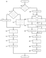
Figure 8a ) shows a flow chart of a prior-art method.Step 60 ofFigure 8a ) comprises a pre-assembly of the system, followed bystep 61 where an initial alignment in up to six degrees of freedom can be made. Instep 62, glue is added on to one or more washers, which are then assembled onto the system instep 63. A final alignment in up to six degrees of freedom can be made instep 64. The glue can then be cured instep 65. If glue is applied to the system before alignment, it can be redistributed during the alignment. Additionally, if there is no control of the shape of the size of the cavities where glue can penetrate, there can be formation of glue wedges which give rise to curing drift. Further, if the amount of glue that can penetrate such cavities is not limited, the whole cavity can be filled with glue and the curing drift is further increased. -
Figure 8b ) shows flowcharts of one or more embodiments of the present invention. The means for keepingsurfaces device 10 or members located externally, for example in an alignment machine; whereby the selection of one of these such as members located externally or not can be made instep 70. If there is no externally provided force then means to provide such force can be integrated with the connectingdevice 10. Such a determination is made instep 71 of implementation. The force could be provided by anexternal spring 37 that can be manufactured separately and pre-assembled 73 to aseparate member 52, as shown inFigure 16 in order to achieve a pre-assembled system as in 51. - Or the force could be provided by one or
several springs 13 that is/are integrated with the connectingdevice 10, as shown inFigure 5 and/orFigure 6 and/orFigure 7 .Figure 17 (a, b, c or d) shows an example where only onespring member 38 is used. The device ofFigure 17 (a, b, c or d) has two bodies with a gap there between. The twobodies single spring member 38. The twobodies Figure 17 (a, b, c or d) enclose a space which can receive the receivingmember 18. The bodies have at least one hole for insertion of a pin. As shown inFigures 17a-d ) the inside surface of at least one hole can have notches. - With any embodiment of the present invention, there can be an initial alignment between the receiving
member 18 and themember 21 performed in up to six degrees of freedom, instep 74. After the system is initially aligned, fixing compound such as glue or adhesive or potting compound can be applied, instep 75, and a final alignment can be made instep 76, before the fixing compound such as glue or adhesive or potting compound can be cured in 77. - Returning to
Figure 8b ), the means for providing a force to keepsurfaces pre-assembly step 78 is first made and a selection of which optional route is to be selected can be made instep 79. There can be an initial alignment instep 80 in up to six degrees of freedom, followed by the addition of the connectingdevice 10 instep 81 and further a force can be introduced in step 82 to keep 29 and 30 in parallel or in contact. In an alternative embodiment thepre-assembly step 78 can be followed by the immediate addition of a connectingdevice 10 instep 83 and then a force can be introduced instep 84, and the configuration can be submitted to an initial alignment in up to six degrees of freedom instep 85. The two alternatives starting fromstep 78 can end in a common path comprising the steps of adding fixing compound such as glue or adhesive or potting compound instep 86, performing a final alignment in up to six degrees of freedom instep 87, curing the fixing compound such as glue, adhesive or potting compound instep 88 and optionally removing the force that keepssurfaces step 89. - The steps in
Figure 8b ) have the advantage that the fixing compound such as glue or adhesive or potting compound can be applied after initial alignment, so that there can be no redistribution of fixing compound such as glue or adhesive or potting compound during initial alignment. In the case of alignment after fixing compound such as glue or adhesive or potting compound has been introduced, there is the benefit of keeping the amount of fixing compound such as glue or adhesive or potting compound that can enter between thesurfaces Figures 9 to 19 all show modifications to the above embodiments. The members shown inFigures 9 to 12 are the same design as used inFigures 6 and7 . -
Figures 9 to 12 all show a device or system for connecting a pin and a member comprising a pin, and a receiving member having a receiving planar surface with at least one opening.Figures 9 to 19 show a system that can be used in an optical engine wherein a member in the shape of a pin can be joined with an image device receiving member having a hole. The hole must be big enough to provide space between the pin and the receiving member to allow some freedom of movement for the alignment process and to deal with component/assembly dimensional tolerances. A connecting device is provided having a main body with a contact plane, said main body having at least one opening, where the connecting device is placed with the contact plane towards the receiving planar surface of the receiving member so that an opening of the connecting device overlaps an opening of the receiving surface of the receiving member, and the pin is inserted into said overlap. The connecting and aligning system further comprises means for exerting a force or pressure (e.g. pushing or pulling) between the contact plane of the connecting device and the receiving planar surface of the receiving member to move the contact plane towards the receiving planar surface, wherein the orientation of the pin towards the receiving planar surface of the receiving member can vary with six degrees of freedom, and for all orientations, the contact plane of the connecting device and the receiving planar surface remain parallel to each other. The contact plane can comprise at least three contact points. Also for all orientations, the contact plane of the connecting device and the receiving planar surface stay in contact with each other. - In any of these designs at least one hole need not be fully enclosed.
- In any of these designs the means for exerting a force or pressure (e.g. pushing or pulling) between the contact plane of the connecting device and the receiving planar surface of the receiving member to move the contact plane towards the receiving planar surface, is of mechanical-, magnetic-, gravitational-, electromagnetic-, electrostatic-, adhesive or of pressure differential nature, or any combination of the seven.
- For example,
Figure 9 shows a cross section of a further embodiment of the present invention relating to a system or device for connecting a pin and a member comprising a pin, and a receiving member having a receiving planar surface with at least one opening. The connectingdevice 10 has a main body with a contact plane, said main body having at least one opening, where the connecting device is placed with the contact plane towards the receiving planar surface of a receivingmember 18 so that an opening of the connectingdevice 10 overlaps with an opening of the receiving surface of the receiving member. The connectingdevice 10 can be mounted onto the receivingmember 18 and thepin 21 can be inserted in the resultingchannel 24. The pin is inserted into said overlap. The connecting device also has means (not shown) for exerting a force (e.g. pushing or pulling) between the contact plane of the connectingdevice 10 and the receiving planar surface to bring them together, wherein the orientation of the pin towards the receiving planar surface can vary with six degrees of freedom, and for all orientations, the contact plane of the connectingdevice 10 and the receiving planar surface of the receiving member remain parallel to each other. - The system can be initially aligned. The initial alignment can result in that the
pin 21 is highly asymmetrically positioned within thehole 19. Theaxes axis 22 may have an off-set to the right compared toaxis 20. In general, a parallel off-set can extend in any direction within the XY plane. -
Figure 10 illustrates a variation of embodiment of the present invention described above with respect toFigure 9 . When the alignment has been performed, fixing compound such as glue (or adhesive or potting compound) 23 and 26 can be added to dedicated holes, e.g. such as 17 and/or 25. -
Figure 11 illustrates a further variation of the embodiment of the present invention shown inFigure 9 . During the alignment, themember 18 and thepin 21 can be tilted in two directions, around the X axis and/or around the Y axis, and at the same time shifted in the XY plane. This is determined by the relationship between the size of the holes through which thepin 21 is inserted and the outer diameter of thepin 21 -
Figure 12 illustrates a variation of the embodiment of the present invention illustrated inFigure 11 . After the alignment has been performed, fixing compound such as glue or adhesive or pottingcompound - An advantage of embodiments of the present invention is that they can avoid or reduce an asymmetrical configuration after the alignment, such as can occur with a prior-art system, which would give rise to asymmetrical glue distribution. This would in turn result in asymmetrical shrinking and curing drift. The present invention avoids this problem since the fixing compound such as glue or adhesive or potting compound distribution is practically independent of the asymmetrical alignment.
- In another embodiment of the present invention (not shown) the means for keeping
surfaces structure 18 or with any structure whereupon thepin 21 is mounted. - In yet another embodiment of the present invention (not shown), the means for keeping
surfaces -
Figure 13, 14 and15 show further examples of embodiments of the connecting device of the present invention. The different bodies can correspond tomember 12 of connectingdevice 10 but can also be used stand-alone, if the means for keepingsurfaces - A rotation of the
pin 21 around itsaxis 22 or a rotation of receivingmember 18 aroundaxis 20 can be possible because of the clearance fit withhole 15. The rotation has no significant effect on the position ofdevice 10. Also here, during a rotation around direction Z of receivingmember 18,surface 29 keeps contact withsurface 30, even ifdevice 10 would rotate a bit around direction Z due to friction components. - The angular freedom between a
centre axis 22 ofpin 21 and acentre axis 16 ofhole 15 of amember 10 can be calculated as a function of: - the outer diameter of
pin 21 - the inner diameter of
hole 15 - the thickness of
body 12. - Despite a tight clearance fit between
pin 21 andhole 15, rotations around the X and Y axis of thepin 21 can be possible due to that the thickness ofmember 12 where it can make contact withpin 21 is small. The rotational freedom around X and/or Y needed during optical alignment is typically limited. So enough angular freedom can be provided. - An advantage of the present invention over prior-art is that the fixing compound such as glue or adhesive of potting compound can be applied after the assembly of 51 and that the largest part of the fixing compound such as glue or adhesive of potting compound will be located on top of the assembly. Since light can access the fixing compound such as glue or adhesive of potting compound, there is no limitation in material choice for the connecting
device 10 so that both transparent and opaque materials (e.g. metals, ceramics, non-transparent oxides or polymers) can be used. With this broad selection of materials, the connecting device can be made locally very thin, for example in the region where it makes contact with the protruding pin. Moreover, it is generally more feasible to achieve a better dimensional accuracy in a thin body compared to a thicker body. A precise through-hole in a sheet metal body can e.g. be made by etching, laser cutting or stamping. A precise through-hole in a thicker glass body might involve drilling and/or grinding. The advantage is that a tighter clearance fit results in a thinner fixing compound such as glue or adhesive ofpotting compound layer 5, which in turn decreases curing drift. - After the initial alignment, the
axes -
Figure 13 shows an example withlocal notches 32 in the perimeter ofhole 15. The number of notches may be e.g. 4 or more or is as required. -
Figure 14 shows examples of different variations of shape and layout of theholes 15 and/or 17.Figure 14c ) has arectangular centre hole 33 that could be used in combination with a rectangular protruding pin. Any other cross-sectional shape of the centre hole is also possible. -
Figure 15a) and 15b ) shows cross-sectional views of embodiments of the connecting device of the present invention where the thickness ofmember 12 is locally reduced at the rim ofhole 15.Figure 15a ) shows astepwise reduction 34 andFigure 15b ) shows acontinuous reduction 35. - This allows a tighter clearance fit without influencing the angular freedom of the pin.
-
Figure 15c ) shows the pin tilt angle alfa, the hole wall thickness t, the hole diameter D and the pin diameter d (and the clearance D-d). When the wall thickness t decreases, a larger pin tilt angle alfa is possible or, when the thickness t decreases; a tighter clearance fit is made possible for the same pin tilt angle.Figure 15c ) shows a local thickness reduction and is a detailed schematic view to understand the pin tilt relation with other parameters. -
Figure 15a) and 15b ) show alternative embodiments of the connecting device of the invention. -
Figure 15b ) shows an example of how the side walls of the surroundingholes 36 may be drafted so that the wall can have an inclination towards the bottom of the hole. One advantage with a drafted hole can be to achieve a higher fixing compound such as glue or adhesive or potting compound retention strength, e.g. due to an undercut ofdevice 10 towards the fixing compound such as glue or adhesive of potting compound. So this embodiment can bring at least one or any combination of the advantages of - a smaller contact surface between the pin and the hole so that the clearance fit can be made smaller,
and/or - a higher fixing compound retention strength such as glue, adhesive or potting compound retention strength in
holes 36 due to the undercut,
and/or - manufacturing processes, e.g. the draft angle will create a release angle in case injection moulding technologies are used.
- It is shown schematically in
Fig. 15c ) an aspect of the method of the invention for connecting a pin and a member comprising a pin, and a receiving member having a receiving planar surface with at least one opening, a connecting device having a main body with a contact plane, said main body having at least one opening, the method comprising placing the connecting device with the contact plane towards the receiving planar surface so that the at least one opening of the connecting device overlaps the at least one opening of the receiving surface, and inserting the pin into said overlap, wherein at least one opening is a drafted opening. -
Figure 16 shows an example of an embodiment of a part of the present invention where the means for keepingsurface external member 37 assembled ontomember 12. Advantages with this solution could be e.g. to facilitate manufacturing and to reduce cost. Thespring feature 37 can be separately manufactured and then assembled to asingle part 52 that corresponds to 12 of the connectingdevice 10. This embodiment also shows an alternative configuration oflocal notches 32 in the centre hole. -
Figure 17 shows examples of two embodiments of a part of the present invention where the means for keepingsurface member 38. The b) and d) figures show different configuration ofmember 12. The a) and c) shows the same devices viewed from below. -
Figure 18 shows examples of embodiments of a part of the present invention where the hole inmember 11 can be replaced with anopening 39 which is not completely closed. In another embodiment (not shown) themember 18 could comprise anopening 19 that is not completely enclosed. -
Figure 19 shows examples of embodiments of a part of the present invention where in a) the centre hole inmember 12 can be cross shaped and the fixing compound such as glue holes 17 do not have to be closed, and in b) the connectingmembers 13 are not sharing thesame member 11, and are also located opposite each other. -
Figure 20a-c ) show further embodiments of the present invention wherein a "spring function" provided with, e.g. is connected to the pin. In thesedrawings body 11 is not shown.Figure 20 shows an embodiment of the present invention relating to a system and method for connecting a pin and a member comprising a pin. The system and devices ofFigure 20 can be used in an optical engine wherein one member is in the shape of a pin that can be joined with an element of the optical engine such as an image device receiving member having a hole. The hole is big enough to provide space between the pin and the receiving member to allow some freedom of movement for the alignment process and to deal with component/assembly dimensional tolerances. InFigure 20a-c ), a connectingdevice 10 is shown that can have one substantially planar body, 12. Instead of one, two or more connectingmembers 13 the means for exerting a force is provided by anelement 45. - The connecting
device 10 can be made of any suitable material such as metal, polymers or ceramics, or any combination of the three.Body 12 has a hole located near or at the centre ofbody 12. This hole is arranged to receive a protrudingpin 21. The hole can provide a pre-centering function, for example, to said protruding pin so that it can guide the pin closer to its final position. As can be understood from the above, the connectingdevice 10 has a receiving planar surface, e.g. one ofsurfaces body 12 with at least one opening. Themember 45 provides an elastic spring function, which can provide a force exerted (e.g. pushing or pulling) onbody 12 to move it towards the receivingmember 18. -
Figure 20a ) shows an alternative embodiment of the means for exerting a force (45) between the contact plane "12" of the connectingdevice 10 and the receivingplanar surface 30 of the receivingmember 18. It comprisesextensions 47 that "click into" thegrooves 48 of thepin 21. The supports 46 rest on the member "12", for example inFigure 20c). Figure 20b ) shows how member "12" is mounted onto the receivingmember 18 and thepin 21 has been inserted throughchannel 24.Member 45 is then added on top of "12" as shown inFigure 20c ). - The described examples should not limit the present invention. For example the shape, size and position of the
centre hole 15 can differ. Thehole 15 can for example take any shape that matches to a protruding element, e.g. round, rectangular, square, cross, etc. The shape, size, amount and position of theholes 17 or openings as 39 may also differ. In one extreme situation it could be possible to work without fixing compound such as glue holes 17 and apply glue on the outer edges ofplanar body 12. To allow this, surface 30 ofmember 18 could be made bigger thanmember 12. The shape, size, quantity and position of the local notches around thehole 15 can also differ or they can be absent. - The connecting
members 13, if present, can also differ in shape, size, quantity and position. As described above they can be integrated inmember Body 11 could be split up in several bodies, each being connected by anindividual member 13 toplanar body 12. - The protruding features 28 of
body 11, if present, can also differ in shape, size, quantity and position. They are also not limited to a specific shape but could be e.g. spherical, cylindrical, etc. Furthermore, they could be provided by additional members assembled ontomember 11. Although less ideal, thefeatures 28 could be provided ontomember 18. - The means for keeping
surfaces device 10, or can be provided by the alignment tool. The means could even be provided by a member ofmember 18 or a member of an optical engine. The character of the above mentioned means can be a mechanical force, e.g. as in the case ofmembers 13. An alternative implementation could be to use an air-pressure differential, a magnetic force or gravity, etc. A combination of all alternative means could of course also be used. - The means could even be provided by a member, assembled onto the protruding
member 21, after thepre-assembled system 51 is made.
Claims (17)
- A connecting and aligning system the system comprising a pin (21) and a receiving member (18) having a receiving planar surface (30) with at least one opening (19) being big enough to provide space between the pin (21) and the receiving member (18) to allow freedom of movement for an alignment process, wherein the system further comprises a connecting device (10) having a main body (12) with a contact plane (29), said main body (12) having at least one opening (15) whereby the connecting device (10) is placed with the contact plane (29) towards the receiving planar surface (30) so that the at least one opening (15) of the connecting device (10) overlaps the at least one opening (19) of the receiving surface (30), and the pin (21) is inserted into said overlap, said system further comprising means for exerting a force between the contact plane (29) of the connecting device (10) and the receiving planar surface (30) of the receiving member (18), wherein the orientation of the pin (21) with respect to the receiving planar surface (30) of the receiving member (18) can vary with six degrees of freedom in the alignment process, and characterized in that, for all orientations, the contact plane (29) of the connecting device (10) and the receiving planar surface (30) of the receiving member (18) remain parallel to each other.
- A system according to claim 1, wherein the contact plane (29) comprises at least three contact points.
- A system according to any of the above claims, wherein for all orientations, the contact plane (29) of the connecting device (10) and the receiving planar surface (30) of the receiving member (18) stay in contact with each other.
- A system according to any of the above claims, wherein at least one opening is not fully enclosed, or at least one opening (15) of the main body (12) of the connecting device (10) is of arbitrary shape, at least one opening (15) of the main body (12) of the connecting device (10) is circular, oval, square, rectangular or triangular or any combination of any of the five, or the walls of at least one opening (15) of the main body (12) of the connecting device (10) have notches.
- A system according to any of the above claims, wherein means for exerting a force between the contact plane (29) of the connecting device (10) and the receiving planar surface (30) of the receiving member (18) is of mechanical-, magnetic-, gravitational-, electromagnetic-, electrostatic-, adhesive or of pressure differential nature, or any combination of any number of the seven, and/orthe means for exerting a force between the contact plane (29) of the connecting device (10) and the receiving planar surface (30) of the receiving member (18), is provided externally, for example by an alignment machine and/orthe means for exerting a force between the contact plane (29) of the connecting device (10) and the receiving planar surface (30) of the receiving member (18) is attached to the pin (21), and/orto the connecting device (10).
- A system according to claim 5, wherein the means for exerting a force between the contact plane (29) and the receiving planar surface (30) of the receiving member (18) comprises an elastic member (13, 37, 38, 45) that is integrated with the connecting device (10) or is attached to the receiving member (18) so that it clamps the connecting device (10) to the receiving member (18).
- A system according to claim 6, wherein the means for exerting a force between the contact plane (29) and the receiving planar surface (30) of the receiving member (18) comprises at least one second surface (11), distant from the contact plane (29), and at least one elastic member (13, 38) connecting the at least one second surface (11) with the contact plane (29).
- A system according to claim 7, wherein the second surface (11) is having spherical or cylindrical elevations (28) that make contact with the receiving member (18).
- A system according to any of the above claims, wherein the height of the sidewalls of any of the openings (15, 17) of the main body (12) of the connecting device (10) are smaller than the thickness of the rest of the connecting device (10).
- A method for connecting and aligning a pin (21) and a receiving member (18), having a receiving planar surface (30) with at least one opening (19) being big enough to provide space between the pin (21) and the receiving member (18) to allow freedom of movement for an alignment process, with a connecting device (10) having a main body (12) with a contact plane (29), said main body (12) having at least one opening (15), the method comprising:placing the connecting device (10) with the contact plane (29) towards the receiving planar surface (30) so that an opening (15) of the connecting device (10) overlaps an opening (19) of the receiving surface (30), and inserting the pin (21) into said overlap, exerting a force between the contact plane (29) of the connecting device (10) and the receiving planar surface (30),wherein the orientation of the pin (21) towards the receiving planar surface (30) can vary with six degrees of freedom in the alignment process, and wherein the method is characterized in that, for all orientations, the contact plane (29) of the connecting device (10) and the receiving planar surface (30) of the receiving member (18) remain parallel to each other.
- A method according to claim 10, wherein the step of exerting a force between the contact plane (29) of the connecting device (10) and the receiving planar surface (30) of the receiving member (10) is by any of mechanical-, magnetic-, gravitational-, electromagnetic-, electrostatic-, adhesive or of pressure differential nature, or any combination of any number of the seven, and/orthe step of exerting a force between the contact plane (29) of the connecting device (10) and the receiving planar surface (30) of the receiving member (18), is provided externally, for example by an alignment machine, and/orthe step of exerting a force between the contact plane (29) of the connecting device (10) and the receiving planar surface (30) of the receiving member (10) is performed by means attached to the pin (21), and/orthe step of exerting a force between the contact plane (29) of the connecting device (10) and the receiving planar surface (30) of the receiving member (18) is performed by means attached to the connecting device (10) or attached to the receiving member (18).
- A method according to claim 11, wherein the step of exerting a force between the contact plane (29) and the receiving planar surface (30) of the receiving member (18) clamps the connecting device (10) to the receiving member (18).
- A method according to claim 10, the method further comprising the steps ofPreparing the system, without glue applied,Aligning the system,Adding glue (23, 26) to the system, andPost-treating the system.
- A method according to claim 13, wherein preparing the system comprises the step of adding means for providing a force to the connecting device (10) in order to keep the connecting device (10) in parallel or in contact with the receiving member (18).
- A method according to claim 13, wherein aligning the system comprises the steps of
Exerting a force to keep the receiving member (18) and the connecting device (10) in parallel or in contact with each other, while moving the pin (21) and the receiving member (18) relative to each other in up to six degrees of freedom. - A method according to claim 13, wherein the step of post treatment comprises the step of performing alignment before curing the glue (23, 26), or
the step of post treatment comprises the step of removing the means for providing a force. - Use of the system according to any of the claims 1 to 9 in an optical engine.
Applications Claiming Priority (1)
| Application Number | Priority Date | Filing Date | Title |
|---|---|---|---|
| PCT/EP2015/051408 WO2016116170A1 (en) | 2015-01-23 | 2015-01-23 | Connecting device for improved alignment |
Publications (2)
| Publication Number | Publication Date |
|---|---|
| EP3247914A1 EP3247914A1 (en) | 2017-11-29 |
| EP3247914B1 true EP3247914B1 (en) | 2023-08-16 |
Family
ID=52484436
Family Applications (1)
| Application Number | Title | Priority Date | Filing Date |
|---|---|---|---|
| EP15705212.7A Active EP3247914B1 (en) | 2015-01-23 | 2015-01-23 | Connecting device for improved alignment |
Country Status (4)
| Country | Link |
|---|---|
| US (1) | US10851822B2 (en) |
| EP (1) | EP3247914B1 (en) |
| CN (1) | CN107980083B (en) |
| WO (1) | WO2016116170A1 (en) |
Families Citing this family (4)
| Publication number | Priority date | Publication date | Assignee | Title |
|---|---|---|---|---|
| US20200024492A1 (en) * | 2018-07-20 | 2020-01-23 | Apple Inc. | Using magnetic fields to increase the bonding area of an adhesive joint |
| GB2582631A (en) * | 2019-03-28 | 2020-09-30 | Airbus Operations Ltd | A joint for an aircraft assembly |
| CN112643820B (en) * | 2020-09-28 | 2022-06-17 | 湖南潇龙机械设备制造有限责任公司 | Hot air device for door plate edge bonding machine |
| JP7224081B1 (en) * | 2022-12-02 | 2023-02-17 | 株式会社Braing | Fixing jig for welding and manufacturing method of welding work |
Family Cites Families (52)
| Publication number | Priority date | Publication date | Assignee | Title |
|---|---|---|---|---|
| US2236850A (en) * | 1939-10-21 | 1941-04-01 | Tinnerman Products Inc | Fastening device |
| US2363210A (en) * | 1943-10-12 | 1944-11-21 | Tinnerman Products Inc | Fastening device |
| US2400270A (en) * | 1943-11-13 | 1946-05-14 | Tinnerman Products Inc | Fastening device |
| US2378258A (en) * | 1944-01-06 | 1945-06-12 | Tinnerman Products Inc | Fastening device |
| US2378684A (en) * | 1944-10-28 | 1945-06-19 | Worcester Stamped Metal Compan | Lock nut |
| US2558720A (en) * | 1946-07-19 | 1951-07-03 | Tinnerman Products Inc | Fastener |
| US2822198A (en) * | 1956-02-20 | 1958-02-04 | Gen Motors Corp | Fastener means |
| GB861050A (en) * | 1958-02-05 | 1961-02-15 | Ft Products Ltd | An improved fastener |
| US3007725A (en) * | 1959-06-08 | 1961-11-07 | United Carr Fastener Corp | Fastening device |
| US3217773A (en) * | 1964-08-24 | 1965-11-16 | Bishop & Babcock Corp | Sheet metal clip with nut means and spacing embossures |
| FR2010335A6 (en) * | 1968-06-07 | 1970-02-13 | Raymond A Ste | |
| US3669170A (en) * | 1970-06-22 | 1972-06-13 | Westinghouse Electric Corp | U-shaped clip nut |
| US3680900A (en) * | 1971-04-07 | 1972-08-01 | Aisin Seiki | Coupling member |
| US3927707A (en) * | 1973-10-11 | 1975-12-23 | Trw Inc | Clip nut |
| US4050831A (en) * | 1976-09-15 | 1977-09-27 | Outboard Marine Corporation | Unitary bushing and retainer assembly |
| US4402640A (en) * | 1980-10-17 | 1983-09-06 | Illinois Tool Works Inc. | Clinch nut for plastic panels |
| DE3536473A1 (en) * | 1985-10-12 | 1987-04-16 | Raymond A Fa | SELF-LOCKING CLAMP TYPE NUT |
| DE3542841A1 (en) * | 1985-12-04 | 1987-06-11 | Raymond A Fa | CLAMP TYPE NUT WITH MOUNTING DEVICE |
| US4836007A (en) * | 1986-09-08 | 1989-06-06 | Saccoccio August J | Method of forming a nut-like member |
| FR2627554B1 (en) * | 1988-02-24 | 1990-08-10 | Rapid Sa | IMPROVED FIXING DEVICE FORMING A CLAMP AND ANY PART PROVIDED WITH THIS DEVICE |
| DE8809756U1 (en) * | 1988-07-30 | 1988-10-06 | Ejot Eberhard Jaeger Gmbh & Co Kg, 5928 Bad Laasphe, De | |
| DE3910423A1 (en) * | 1989-03-31 | 1990-10-04 | Raymond A Fa | CLAMP TYPE NUT FOR AUTOMATIC ASSEMBLY |
| US5423646A (en) * | 1993-02-24 | 1995-06-13 | Buell Industries, Inc. | U-nut |
| US5306091A (en) * | 1993-07-19 | 1994-04-26 | Saturn Corporation | Sheet metal nut |
| US5458365A (en) * | 1993-08-03 | 1995-10-17 | Morton International, Inc. | Adjustable snap away fastener |
| US5294224A (en) * | 1993-08-16 | 1994-03-15 | General Motors Corporation | C-shaped fastening clip with improved strength |
| US5588666A (en) * | 1994-06-27 | 1996-12-31 | Izumi Corporation | Driver side air bag cover mounting assembly |
| JPH08207783A (en) * | 1994-12-07 | 1996-08-13 | Toyoda Gosei Co Ltd | Steering wheel |
| CA2171918C (en) * | 1995-05-26 | 2000-06-06 | Michael G. Gagnon | U-nut |
| US5653147A (en) * | 1995-08-10 | 1997-08-05 | Teleflex Incorporated | Expandable retainer for conduit end fitting |
| US5603524A (en) * | 1995-12-01 | 1997-02-18 | General Motors Corporation | Releasable fastener for air bag deployment cover |
| US5700103A (en) * | 1996-07-08 | 1997-12-23 | Tsai; Chun-Hsin | Mounting structure |
| DE29616933U1 (en) * | 1996-09-18 | 1998-01-22 | Siemens Ag | Latching device for a linearly displaceable component |
| US5755458A (en) * | 1996-12-11 | 1998-05-26 | Textron Inc. | Slide-in and snap-fit air bag mounting arrangement |
| US5961264A (en) * | 1998-03-10 | 1999-10-05 | Transtechnology Corp. | Multi-threaded nut assembly having tilted barrel section |
| US6476986B2 (en) * | 1999-12-28 | 2002-11-05 | Texas Instruments Incorporated | Six-axis attachment apparatus and method for spatial light modulators |
| US6842949B2 (en) * | 2003-05-19 | 2005-01-18 | Robert E. Warren | U-shaped wire rope clamp |
| AU2005279288A1 (en) * | 2004-09-02 | 2006-03-09 | Ejot Gmbh & Co. Kg | U-shaped clamp |
| DE102005012605B4 (en) * | 2005-03-18 | 2007-07-05 | A. Raymond Et Cie | Device for connecting a fastening part to a component |
| JP4646756B2 (en) * | 2005-09-20 | 2011-03-09 | 株式会社パイオラックス | Shaft fixing structure |
| JP4900919B2 (en) * | 2006-07-19 | 2012-03-21 | ダイキョーニシカワ株式会社 | Interior member for vehicle and method for removing the same |
| DE102007036554B4 (en) * | 2007-07-25 | 2009-06-25 | Getrag Getriebe- Und Zahnradfabrik Hermann Hagenmeyer Gmbh & Cie Kg | Lid-bearing assembly and method for mounting an actuator shaft |
| US8272803B2 (en) * | 2010-01-21 | 2012-09-25 | Laitram, L.L.C. | Conveyor shaft assembly with spring clip |
| CH704129B1 (en) * | 2010-11-25 | 2020-09-30 | Eta Sa Mft Horlogere Suisse | Device for positioning a bridge on a plate. |
| US8602445B2 (en) * | 2011-09-21 | 2013-12-10 | Chrysler Group Llc | Attachment clip |
| US9346593B2 (en) * | 2011-11-10 | 2016-05-24 | Oldcastle Precast, Inc. | Tamper resistant closure mechanism for a utility vault |
| CN102493986A (en) | 2011-12-06 | 2012-06-13 | 中国科学院长春光学精密机械与物理研究所 | Splicing tool with precise and controllable glue layer thickness |
| DE102012205837B4 (en) * | 2012-04-11 | 2016-07-21 | Bayerische Motoren Werke Aktiengesellschaft | A connection between components |
| JP5666656B2 (en) * | 2013-07-08 | 2015-02-12 | 株式会社ホンダアクセス | Part mounting structure for plate-like members |
| US9490743B2 (en) * | 2014-05-28 | 2016-11-08 | Sunedison, Inc. | Grounding clips and tabs for mounting components to solar modules |
| CN204739068U (en) * | 2015-07-14 | 2015-11-04 | 上海上飞飞机装备制造有限公司 | Take sealed layer board self -locking nut that moves about of novel bonding formula of elastic mounting fixture |
| US10156183B2 (en) * | 2016-11-30 | 2018-12-18 | GM Global Technology Operations LLC | Anti-rattle devices and turbocharger wastegate assemblies including the same |
-
2015
- 2015-01-23 US US15/544,608 patent/US10851822B2/en active Active
- 2015-01-23 EP EP15705212.7A patent/EP3247914B1/en active Active
- 2015-01-23 CN CN201580074241.3A patent/CN107980083B/en active Active
- 2015-01-23 WO PCT/EP2015/051408 patent/WO2016116170A1/en active Application Filing
Also Published As
| Publication number | Publication date |
|---|---|
| CN107980083A (en) | 2018-05-01 |
| WO2016116170A1 (en) | 2016-07-28 |
| EP3247914A1 (en) | 2017-11-29 |
| CN107980083B (en) | 2020-12-01 |
| US10851822B2 (en) | 2020-12-01 |
| US20170370390A1 (en) | 2017-12-28 |
Similar Documents
| Publication | Publication Date | Title |
|---|---|---|
| EP3247914B1 (en) | Connecting device for improved alignment | |
| US11073676B2 (en) | Lens unit and method for manufacturing lens unit | |
| EP2193911B1 (en) | Micro lens, method and apparatus for manufacturing micro lens, and camera module including micro lens | |
| JP2007065017A (en) | Lens holding barrel | |
| US20170322478A1 (en) | Autofocus camera and optical device with variable focal length intended to be integrated into such a camera | |
| EP2592457A1 (en) | Lens unit | |
| JP6942604B2 (en) | Imaging device, multi-eye imaging device | |
| US7259923B2 (en) | Lens barrel | |
| CN108351485B (en) | Camera module and method of manufacturing the same | |
| US8408816B2 (en) | Optical connector | |
| US20180007246A1 (en) | Manufacturing method for camera module, and camera module | |
| CA2746999A1 (en) | Sensor module | |
| JP2018059986A (en) | Imaging device | |
| JP2001051175A (en) | Lens-barrel, its manufacture and positioning device for lens body | |
| JP6390763B1 (en) | Camera module and method for manufacturing camera module | |
| CN112649934B (en) | Optical lens, camera module and assembling method thereof | |
| CN110275263B (en) | Optical lens, camera module and assembling method thereof | |
| JP2006250968A (en) | Projection type display device, and method and device for adjusting and attaching liquid crystal display element for projection type display device | |
| JP2006285109A (en) | Composite optical element and manufacturing method thereof | |
| JP2006156931A (en) | Structure for packaging and correcting in arrangement electric microoptic module simultaneously | |
| US10690877B2 (en) | Optical device comprising a micro-optical system and a retainer, and method for producing an optical device | |
| JP2015031930A (en) | Lens unit | |
| JP2004004577A (en) | Axially displaceable aligning mount for optical components, and method for its manufacture | |
| JP2005092141A (en) | Lens mirror frame, zoom lens barrel, digital camera, and optical apparatus | |
| US9229191B2 (en) | Lens holding structure and method of manufacturing lens holding structure |
Legal Events
| Date | Code | Title | Description |
|---|---|---|---|
| STAA | Information on the status of an ep patent application or granted ep patent |
Free format text: STATUS: THE INTERNATIONAL PUBLICATION HAS BEEN MADE |
|
| PUAI | Public reference made under article 153(3) epc to a published international application that has entered the european phase |
Free format text: ORIGINAL CODE: 0009012 |
|
| STAA | Information on the status of an ep patent application or granted ep patent |
Free format text: STATUS: REQUEST FOR EXAMINATION WAS MADE |
|
| 17P | Request for examination filed |
Effective date: 20170717 |
|
| AK | Designated contracting states |
Kind code of ref document: A1 Designated state(s): AL AT BE BG CH CY CZ DE DK EE ES FI FR GB GR HR HU IE IS IT LI LT LU LV MC MK MT NL NO PL PT RO RS SE SI SK SM TR |
|
| AX | Request for extension of the european patent |
Extension state: BA ME |
|
| DAX | Request for extension of the european patent (deleted) | ||
| STAA | Information on the status of an ep patent application or granted ep patent |
Free format text: STATUS: EXAMINATION IS IN PROGRESS |
|
| 17Q | First examination report despatched |
Effective date: 20210323 |
|
| STAA | Information on the status of an ep patent application or granted ep patent |
Free format text: STATUS: EXAMINATION IS IN PROGRESS |
|
| GRAP | Despatch of communication of intention to grant a patent |
Free format text: ORIGINAL CODE: EPIDOSNIGR1 |
|
| STAA | Information on the status of an ep patent application or granted ep patent |
Free format text: STATUS: GRANT OF PATENT IS INTENDED |
|
| INTG | Intention to grant announced |
Effective date: 20230306 |
|
| GRAS | Grant fee paid |
Free format text: ORIGINAL CODE: EPIDOSNIGR3 |
|
| GRAA | (expected) grant |
Free format text: ORIGINAL CODE: 0009210 |
|
| STAA | Information on the status of an ep patent application or granted ep patent |
Free format text: STATUS: THE PATENT HAS BEEN GRANTED |
|
| AK | Designated contracting states |
Kind code of ref document: B1 Designated state(s): AL AT BE BG CH CY CZ DE DK EE ES FI FR GB GR HR HU IE IS IT LI LT LU LV MC MK MT NL NO PL PT RO RS SE SI SK SM TR |
|
| REG | Reference to a national code |
Ref country code: GB Ref legal event code: FG4D |
|
| REG | Reference to a national code |
Ref country code: CH Ref legal event code: EP |
|
| REG | Reference to a national code |
Ref country code: DE Ref legal event code: R096 Ref document number: 602015085141 Country of ref document: DE |
|
| REG | Reference to a national code |
Ref country code: IE Ref legal event code: FG4D |
|
| P01 | Opt-out of the competence of the unified patent court (upc) registered |
Effective date: 20230811 |
|
| REG | Reference to a national code |
Ref country code: LT Ref legal event code: MG9D |
|
| REG | Reference to a national code |
Ref country code: NL Ref legal event code: MP Effective date: 20230816 |
|
| REG | Reference to a national code |
Ref country code: AT Ref legal event code: MK05 Ref document number: 1600315 Country of ref document: AT Kind code of ref document: T Effective date: 20230816 |
|
| PG25 | Lapsed in a contracting state [announced via postgrant information from national office to epo] |
Ref country code: GR Free format text: LAPSE BECAUSE OF FAILURE TO SUBMIT A TRANSLATION OF THE DESCRIPTION OR TO PAY THE FEE WITHIN THE PRESCRIBED TIME-LIMIT Effective date: 20231117 |
|
| PG25 | Lapsed in a contracting state [announced via postgrant information from national office to epo] |
Ref country code: IS Free format text: LAPSE BECAUSE OF FAILURE TO SUBMIT A TRANSLATION OF THE DESCRIPTION OR TO PAY THE FEE WITHIN THE PRESCRIBED TIME-LIMIT Effective date: 20231216 |
|
| PG25 | Lapsed in a contracting state [announced via postgrant information from national office to epo] |
Ref country code: SE Free format text: LAPSE BECAUSE OF FAILURE TO SUBMIT A TRANSLATION OF THE DESCRIPTION OR TO PAY THE FEE WITHIN THE PRESCRIBED TIME-LIMIT Effective date: 20230816 Ref country code: RS Free format text: LAPSE BECAUSE OF FAILURE TO SUBMIT A TRANSLATION OF THE DESCRIPTION OR TO PAY THE FEE WITHIN THE PRESCRIBED TIME-LIMIT Effective date: 20230816 Ref country code: PT Free format text: LAPSE BECAUSE OF FAILURE TO SUBMIT A TRANSLATION OF THE DESCRIPTION OR TO PAY THE FEE WITHIN THE PRESCRIBED TIME-LIMIT Effective date: 20231218 Ref country code: NO Free format text: LAPSE BECAUSE OF FAILURE TO SUBMIT A TRANSLATION OF THE DESCRIPTION OR TO PAY THE FEE WITHIN THE PRESCRIBED TIME-LIMIT Effective date: 20231116 Ref country code: NL Free format text: LAPSE BECAUSE OF FAILURE TO SUBMIT A TRANSLATION OF THE DESCRIPTION OR TO PAY THE FEE WITHIN THE PRESCRIBED TIME-LIMIT Effective date: 20230816 Ref country code: LV Free format text: LAPSE BECAUSE OF FAILURE TO SUBMIT A TRANSLATION OF THE DESCRIPTION OR TO PAY THE FEE WITHIN THE PRESCRIBED TIME-LIMIT Effective date: 20230816 Ref country code: LT Free format text: LAPSE BECAUSE OF FAILURE TO SUBMIT A TRANSLATION OF THE DESCRIPTION OR TO PAY THE FEE WITHIN THE PRESCRIBED TIME-LIMIT Effective date: 20230816 Ref country code: IS Free format text: LAPSE BECAUSE OF FAILURE TO SUBMIT A TRANSLATION OF THE DESCRIPTION OR TO PAY THE FEE WITHIN THE PRESCRIBED TIME-LIMIT Effective date: 20231216 Ref country code: HR Free format text: LAPSE BECAUSE OF FAILURE TO SUBMIT A TRANSLATION OF THE DESCRIPTION OR TO PAY THE FEE WITHIN THE PRESCRIBED TIME-LIMIT Effective date: 20230816 Ref country code: GR Free format text: LAPSE BECAUSE OF FAILURE TO SUBMIT A TRANSLATION OF THE DESCRIPTION OR TO PAY THE FEE WITHIN THE PRESCRIBED TIME-LIMIT Effective date: 20231117 Ref country code: FI Free format text: LAPSE BECAUSE OF FAILURE TO SUBMIT A TRANSLATION OF THE DESCRIPTION OR TO PAY THE FEE WITHIN THE PRESCRIBED TIME-LIMIT Effective date: 20230816 Ref country code: AT Free format text: LAPSE BECAUSE OF FAILURE TO SUBMIT A TRANSLATION OF THE DESCRIPTION OR TO PAY THE FEE WITHIN THE PRESCRIBED TIME-LIMIT Effective date: 20230816 |
|
| PG25 | Lapsed in a contracting state [announced via postgrant information from national office to epo] |
Ref country code: PL Free format text: LAPSE BECAUSE OF FAILURE TO SUBMIT A TRANSLATION OF THE DESCRIPTION OR TO PAY THE FEE WITHIN THE PRESCRIBED TIME-LIMIT Effective date: 20230816 |
|
| PG25 | Lapsed in a contracting state [announced via postgrant information from national office to epo] |
Ref country code: ES Free format text: LAPSE BECAUSE OF FAILURE TO SUBMIT A TRANSLATION OF THE DESCRIPTION OR TO PAY THE FEE WITHIN THE PRESCRIBED TIME-LIMIT Effective date: 20230816 |
|
| PG25 | Lapsed in a contracting state [announced via postgrant information from national office to epo] |
Ref country code: SM Free format text: LAPSE BECAUSE OF FAILURE TO SUBMIT A TRANSLATION OF THE DESCRIPTION OR TO PAY THE FEE WITHIN THE PRESCRIBED TIME-LIMIT Effective date: 20230816 Ref country code: RO Free format text: LAPSE BECAUSE OF FAILURE TO SUBMIT A TRANSLATION OF THE DESCRIPTION OR TO PAY THE FEE WITHIN THE PRESCRIBED TIME-LIMIT Effective date: 20230816 Ref country code: ES Free format text: LAPSE BECAUSE OF FAILURE TO SUBMIT A TRANSLATION OF THE DESCRIPTION OR TO PAY THE FEE WITHIN THE PRESCRIBED TIME-LIMIT Effective date: 20230816 Ref country code: EE Free format text: LAPSE BECAUSE OF FAILURE TO SUBMIT A TRANSLATION OF THE DESCRIPTION OR TO PAY THE FEE WITHIN THE PRESCRIBED TIME-LIMIT Effective date: 20230816 Ref country code: DK Free format text: LAPSE BECAUSE OF FAILURE TO SUBMIT A TRANSLATION OF THE DESCRIPTION OR TO PAY THE FEE WITHIN THE PRESCRIBED TIME-LIMIT Effective date: 20230816 Ref country code: CZ Free format text: LAPSE BECAUSE OF FAILURE TO SUBMIT A TRANSLATION OF THE DESCRIPTION OR TO PAY THE FEE WITHIN THE PRESCRIBED TIME-LIMIT Effective date: 20230816 Ref country code: SK Free format text: LAPSE BECAUSE OF FAILURE TO SUBMIT A TRANSLATION OF THE DESCRIPTION OR TO PAY THE FEE WITHIN THE PRESCRIBED TIME-LIMIT Effective date: 20230816 |
|
| PGFP | Annual fee paid to national office [announced via postgrant information from national office to epo] |
Ref country code: DE Payment date: 20240119 Year of fee payment: 10 Ref country code: GB Payment date: 20240124 Year of fee payment: 10 |